EP3329331B1 - Device for shaping a laser beam for an atomic sensor - Google Patents
Device for shaping a laser beam for an atomic sensor Download PDFInfo
- Publication number
- EP3329331B1 EP3329331B1 EP16757293.2A EP16757293A EP3329331B1 EP 3329331 B1 EP3329331 B1 EP 3329331B1 EP 16757293 A EP16757293 A EP 16757293A EP 3329331 B1 EP3329331 B1 EP 3329331B1
- Authority
- EP
- European Patent Office
- Prior art keywords
- laser beam
- retroreflector prism
- plate
- dielectric
- atomic
- Prior art date
- Legal status (The legal status is an assumption and is not a legal conclusion. Google has not performed a legal analysis and makes no representation as to the accuracy of the status listed.)
- Active
Links
- 238000007493 shaping process Methods 0.000 title claims description 20
- 229910052751 metal Inorganic materials 0.000 claims description 35
- 239000002184 metal Substances 0.000 claims description 35
- 230000005540 biological transmission Effects 0.000 claims description 27
- 239000011521 glass Substances 0.000 claims description 20
- 238000000151 deposition Methods 0.000 claims description 9
- 229910052581 Si3N4 Inorganic materials 0.000 claims description 5
- 229910052782 aluminium Inorganic materials 0.000 claims description 5
- XAGFODPZIPBFFR-UHFFFAOYSA-N aluminium Chemical compound [Al] XAGFODPZIPBFFR-UHFFFAOYSA-N 0.000 claims description 5
- PCHJSUWPFVWCPO-UHFFFAOYSA-N gold Chemical compound [Au] PCHJSUWPFVWCPO-UHFFFAOYSA-N 0.000 claims description 5
- 239000010931 gold Substances 0.000 claims description 5
- 229910052737 gold Inorganic materials 0.000 claims description 5
- HQVNEWCFYHHQES-UHFFFAOYSA-N silicon nitride Chemical compound N12[Si]34N5[Si]62N3[Si]51N64 HQVNEWCFYHHQES-UHFFFAOYSA-N 0.000 claims description 5
- 238000011144 upstream manufacturing Methods 0.000 claims description 5
- 238000005530 etching Methods 0.000 claims description 4
- 238000004519 manufacturing process Methods 0.000 claims description 4
- 238000000034 method Methods 0.000 claims description 4
- 239000003989 dielectric material Substances 0.000 claims description 3
- 239000007769 metal material Substances 0.000 claims description 2
- 239000004411 aluminium Substances 0.000 claims 2
- 230000010287 polarization Effects 0.000 description 26
- 230000003287 optical effect Effects 0.000 description 9
- 229910052792 caesium Inorganic materials 0.000 description 6
- TVFDJXOCXUVLDH-UHFFFAOYSA-N caesium atom Chemical compound [Cs] TVFDJXOCXUVLDH-UHFFFAOYSA-N 0.000 description 6
- 230000001427 coherent effect Effects 0.000 description 5
- 239000000463 material Substances 0.000 description 4
- 230000010363 phase shift Effects 0.000 description 3
- 238000004611 spectroscopical analysis Methods 0.000 description 3
- VYPSYNLAJGMNEJ-UHFFFAOYSA-N Silicium dioxide Chemical compound O=[Si]=O VYPSYNLAJGMNEJ-UHFFFAOYSA-N 0.000 description 2
- 238000010586 diagram Methods 0.000 description 2
- 238000005259 measurement Methods 0.000 description 2
- 229910052701 rubidium Inorganic materials 0.000 description 2
- IGLNJRXAVVLDKE-UHFFFAOYSA-N rubidium atom Chemical compound [Rb] IGLNJRXAVVLDKE-UHFFFAOYSA-N 0.000 description 2
- 239000000758 substrate Substances 0.000 description 2
- 230000007704 transition Effects 0.000 description 2
- 238000010521 absorption reaction Methods 0.000 description 1
- 230000001133 acceleration Effects 0.000 description 1
- 230000007123 defense Effects 0.000 description 1
- 230000001419 dependent effect Effects 0.000 description 1
- 238000006073 displacement reaction Methods 0.000 description 1
- 230000005684 electric field Effects 0.000 description 1
- 230000005672 electromagnetic field Effects 0.000 description 1
- 238000005516 engineering process Methods 0.000 description 1
- 238000005286 illumination Methods 0.000 description 1
- 230000010354 integration Effects 0.000 description 1
- 238000005459 micromachining Methods 0.000 description 1
- 239000000203 mixture Substances 0.000 description 1
- 238000005329 nanolithography Methods 0.000 description 1
- 230000010355 oscillation Effects 0.000 description 1
- 230000000149 penetrating effect Effects 0.000 description 1
- 230000035515 penetration Effects 0.000 description 1
- 230000000737 periodic effect Effects 0.000 description 1
- 239000012071 phase Substances 0.000 description 1
- 229910052710 silicon Inorganic materials 0.000 description 1
- 239000010703 silicon Substances 0.000 description 1
- 239000000377 silicon dioxide Substances 0.000 description 1
- 238000004513 sizing Methods 0.000 description 1
- HUAUNKAZQWMVFY-UHFFFAOYSA-M sodium;oxocalcium;hydroxide Chemical compound [OH-].[Na+].[Ca]=O HUAUNKAZQWMVFY-UHFFFAOYSA-M 0.000 description 1
- 230000003595 spectral effect Effects 0.000 description 1
- 239000012808 vapor phase Substances 0.000 description 1
- 238000003466 welding Methods 0.000 description 1
Images
Classifications
-
- G—PHYSICS
- G02—OPTICS
- G02B—OPTICAL ELEMENTS, SYSTEMS OR APPARATUS
- G02B27/00—Optical systems or apparatus not provided for by any of the groups G02B1/00 - G02B26/00, G02B30/00
- G02B27/09—Beam shaping, e.g. changing the cross-sectional area, not otherwise provided for
- G02B27/0938—Using specific optical elements
- G02B27/095—Refractive optical elements
- G02B27/0972—Prisms
-
- G—PHYSICS
- G02—OPTICS
- G02B—OPTICAL ELEMENTS, SYSTEMS OR APPARATUS
- G02B27/00—Optical systems or apparatus not provided for by any of the groups G02B1/00 - G02B26/00, G02B30/00
- G02B27/28—Optical systems or apparatus not provided for by any of the groups G02B1/00 - G02B26/00, G02B30/00 for polarising
-
- G—PHYSICS
- G02—OPTICS
- G02B—OPTICAL ELEMENTS, SYSTEMS OR APPARATUS
- G02B5/00—Optical elements other than lenses
- G02B5/04—Prisms
-
- G—PHYSICS
- G02—OPTICS
- G02B—OPTICAL ELEMENTS, SYSTEMS OR APPARATUS
- G02B5/00—Optical elements other than lenses
- G02B5/12—Reflex reflectors
- G02B5/122—Reflex reflectors cube corner, trihedral or triple reflector type
-
- G—PHYSICS
- G02—OPTICS
- G02B—OPTICAL ELEMENTS, SYSTEMS OR APPARATUS
- G02B5/00—Optical elements other than lenses
- G02B5/30—Polarising elements
- G02B5/3025—Polarisers, i.e. arrangements capable of producing a definite output polarisation state from an unpolarised input state
- G02B5/3058—Polarisers, i.e. arrangements capable of producing a definite output polarisation state from an unpolarised input state comprising electrically conductive elements, e.g. wire grids, conductive particles
-
- G—PHYSICS
- G02—OPTICS
- G02B—OPTICAL ELEMENTS, SYSTEMS OR APPARATUS
- G02B5/00—Optical elements other than lenses
- G02B5/30—Polarising elements
- G02B5/3083—Birefringent or phase retarding elements
-
- G—PHYSICS
- G04—HOROLOGY
- G04F—TIME-INTERVAL MEASURING
- G04F5/00—Apparatus for producing preselected time intervals for use as timing standards
- G04F5/14—Apparatus for producing preselected time intervals for use as timing standards using atomic clocks
- G04F5/145—Apparatus for producing preselected time intervals for use as timing standards using atomic clocks using Coherent Population Trapping
Definitions
- the invention relates to the field of atomic sensors comprising alkaline vapor cells and laser beam shaping devices as well as laser beam shaping devices for such atomic sensors.
- a typical atomic sensor according to the invention is a chip-scale atomic clock, known by the acronym CSAC (for Chip-Scale Atomic Clock).
- CSAC Chip-Scale Atomic Clock
- An example is the CSAC called SA.45s from the company MICROSEMI which has a volume of 16 cm3, a mass of 35 g and requires a power of only 120 mW.
- Such an atomic micro-clock is also known from the work of the MAC-TFC consortium, the FEMTO-ST institute (acronym for Franche-Comté Electronique Mécanique Thermique et Optique - Sciences et Technologies) which has developed a very compact cesium vapor cell (a few mm3), with micro-machining MEMS (acronym for MicroElectroMechanical Systems) of the silicon and anodic welding (see for example “New approach of fabrication and dispensing of micromachined cesium vapor cell” by L. Nieradko, C. Gorecki, A. Douahi, V. Giordano, JC Beugnot, J. Dziuban and M. Moraja published in JOURNAL OF MICRO-NANOLITHOGRAPHY MEMS AND MOEMS August 2008 ).
- Such a cell has an optical window diameter of approximately 2 millimeters.
- the beam from such a vertical cavity laser is characterized by relatively low divergence (FWHM 10-15°) and size (about 20 microns at the output mirror).
- the invention finally relates to an atomic sensor comprising a device for shaping a laser beam as defined in claim 11.
- the dependent claims define additional embodiments.
- the retro-reflecting prism 9 comprises an entry zone 12 for an incoming laser beam 5b, an exit zone 13 for an outgoing laser beam 5d as well as two reflection faces 14, 15 for an internal laser beam 5c .
- Such a plane of section H of the retro-reflector prism 9 is in particular a plane perpendicular to the direction of intersection I between respective geometric planes of extension P1, P2 of the two reflection faces 14, 15.
- the metal strips 18 are also juxtaposed with respect to each other in a passing direction DP of the metal network 17 perpendicular to the direction of the metal strip DM.
- the geometric plane of extension PL of the dielectric network 20 can be parallel to the geometric plane of extension PP of the metal network 17.
Description
L'invention concerne le domaine des capteurs atomiques comportant des cellules à vapeur alcaline et des dispositifs de mise en forme de faisceau laser ainsi que les dispositifs de mise en forme de faisceau laser pour de tels capteurs atomiques.The invention relates to the field of atomic sensors comprising alkaline vapor cells and laser beam shaping devices as well as laser beam shaping devices for such atomic sensors.
Les capteurs atomiques sont notamment des horloges atomiques, des micro-magnétomètres ou encore des microgyromètres. De tels capteurs atomiques peuvent par exemple être destinés aux systèmes de télécommunication, navigation et défense.The atomic sensors are in particular atomic clocks, micro-magnetometers or even microgyrometers. Such atomic sensors can for example be intended for telecommunications, navigation and defense systems.
De tels capteurs sont parfois qualifiés de « microhorloges atomiques », « micro-magnétomètres » et « microgyromètres ». Dans l'ensemble du texte, le terme « micro » doit être compris dans le contexte et avec le sens indiqués.Such sensors are sometimes referred to as “atomic microclocks”, “micro-magnetometers” and “microgyrometers”. Throughout the text, the term “microphone” must be understood in the context and with the meaning indicated.
Le fonctionnement des capteurs atomiques repose sur une spectroscopie optique des atomes d'un gaz emplissant une cavité munie d'une fenêtre optique. Le gaz est usuellement une vapeur alcaline, comme du césium ou du rubidium. Cette spectroscopie permet de mesurer une ou plusieurs grandeurs spectrales associées à la ou les quantités physiques que le capteur cherche à observer, par exemple une fréquence, une période temporelle, un champ magnétique ou une accélération.The operation of atomic sensors is based on an optical spectroscopy of the atoms of a gas filling a cavity equipped with an optical window. The gas is usually an alkaline vapor, such as cesium or rubidium. This spectroscopy makes it possible to measure one or more spectral quantities associated with the physical quantity or quantities that the sensor seeks to observe, for example a frequency, a time period, a magnetic field or an acceleration.
De tels capteurs atomiques offrent l'intérêt d'être de petites tailles, économes en énergie et de présenter une très bonne précision et stabilité de mesure.Such atomic sensors have the advantage of being small in size, energy efficient and of having very good measurement accuracy and stability.
Un capteur atomique typique selon l'invention est une horloge atomique à l'échelle d'une puce, connue sous l'acronyme CSAC (pour Chip-Scale Atomic Clock). Un exemple en est la CSAC dénommée SA.45s de la société MICROSEMI qui présente un volume de 16 cm3, une masse de 35 g et nécessite une puissance de seulement 120mW.A typical atomic sensor according to the invention is a chip-scale atomic clock, known by the acronym CSAC (for Chip-Scale Atomic Clock). An example is the CSAC called SA.45s from the company MICROSEMI which has a volume of 16 cm3, a mass of 35 g and requires a power of only 120 mW.
Dans le cas d'une micro-horloge atomique, le fonctionnement du capteur est usuellement basé sur la mesure de la fréquence d'une transition micro-onde particulière des atomes du gaz, dite transition d'horloge et met en œuvre le principe de la résonnance atomique par piégeage cohérent de population connu sous l'acronyme CPT (pour Coherent Population Trapping).In the case of an atomic micro-clock, the operation of the sensor is usually based on the measurement of the frequency of a particular microwave transition of the atoms of the gas, called clock transition and implements the principle of atomic resonance by coherent population trapping known by the acronym CPT (for Coherent Population Trapping).
Une telle micro-horloge atomique est également connu des travaux du consortium MAC-TFC, l'institut FEMTO-ST (acronyme pour Franche-Comté Electronique Mécanique Thermique et Optique - Sciences et Technologies) qui a développé une cellule à vapeur de césium très compacte (quelques mm3), avec micro-usinage MEMS (acronyme pour MicroElectroMechanical Systems) du silicium et soudure anodique (voir par exemple
Cette cellule a une architecture dite « transmissive », le laser, un laser à cavité verticale connu sous l'acronyme VCSEL (pour Vertical Cavity Surface Emitting Laser), et le photo détecteur, (photodiode) étant situés de part et d'autre de la cellule proprement dite, le faisceau laser la traversant de part en part, y entrant par le premier couvercle en verre et en sortant par le second couvercle en verre.This cell has a so-called "transmissive" architecture, the laser, a vertical cavity laser known by the acronym VCSEL (for Vertical Cavity Surface Emitting Laser), and the photo detector (photodiode) being located on either side of the actual cell, the laser beam passing right through it, entering it through the first glass cover and leaving through the second glass cover.
Le faisceau issu d'un tel laser à cavité verticale est caractérisé par une divergence (FWHM 10-15°) et une taille (de l'ordre de 20 microns au niveau du miroir de sortie) relativement faibles.The beam from such a vertical cavity laser is characterized by relatively low divergence (FWHM 10-15°) and size (about 20 microns at the output mirror).
Ainsi, la distance requise pour atteindre un diamètre de faisceau correspondant à la fenêtre optique de la cellule et permettant d'éclairer l'ensemble des atomes, si possible avec des intensités équivalentes (illumination uniforme), est donc élevée si aucun dispositif supplémentaire n'est ajouté, ce qui limite la taille minimale du capteur atomique.Thus, the distance required to reach a beam diameter corresponding to the optical window of the cell and making it possible to illuminate all the atoms, if possible with equivalent intensities (uniform illumination), is therefore high if no additional device is present. is added, which limits the minimum size of the atomic sensor.
Pour cela, dans le cadre du consortium MAC-TFC, a été développé un système télescopique permettant d'augmenter la divergence du faisceau et de collimater le faisceau avant son entrée dans la cellule.For this, within the framework of the MAC-TFC consortium, a telescopic system has been developed to increase the divergence of the beam and to collimate the beam before it enters the cell.
Une telle solution permet de réduire l'encombrement mais implique un alignement de plusieurs composants optiques qui est une opération délicate aux dimensions de la cellule.Such a solution makes it possible to reduce the bulk but involves an alignment of several optical components which is a delicate operation given the dimensions of the cell.
Une autre solution est notamment connue du document
Une telle solution permet de s'affranchir d'alignements contraignants. En effet, contrairement aux lentilles, un mauvais positionnement du système de repli (en translation) n'est pas plus dommageable que le serait la même erreur de positionnement de la source ou de la cellule.Such a solution makes it possible to dispense with constraining alignments. Indeed, unlike lenses, poor positioning of the fallback system (in translation) is no more damaging than the same positioning error of the source or of the cell.
L'utilisation d'un prisme présente à cet égard l'intérêt, par rapport à des miroirs diélectriques (présentant également une faible absorption) d'offrir un excellent contrôle de l'orientation des surfaces réfléchissantes. En effet, la tolérance angulaire est en général spécifiée à ±15 arcsec (±0.004°) même pour des prismes de quelques millimètres de côté.The use of a prism has in this respect the advantage, compared to dielectric mirrors (also having low absorption) of offering a excellent control of the orientation of reflective surfaces. Indeed, the angular tolerance is generally specified at ±15 arcsec (±0.004°) even for prisms with a side of a few millimeters.
Toutefois, la spectroscopie de la vapeur alcaline par le mécanisme du piégeage cohérent de population requiert un faisceau laser entrant dans la cellule dont l'état de polarisation est circulaire.However, the spectroscopy of alkaline vapor by the mechanism of coherent population trapping requires a laser beam entering the cell whose state of polarization is circular.
Par ailleurs, les réflexions du faisceau laser dans le prisme peuvent modifier sensiblement la polarisation du faisceau laser. En effet, même si le faisceau lumineux ne quitte par le prisme lorsque l'angle d'incidence est supérieur à l'angle critique défini plus haut (i.e. il n'y a pas de flux d'énergie à travers le dioptre), le champ électromagnétique pénètre en revanche légèrement dans le milieu extérieur, avec des profondeurs de pénétration différentes selon l'orientation du champ électrique (parallèle ou perpendiculaire au plan d'incidence). Les deux composantes du faisceau laser subissant des déphasages différents, un faisceau laser polarisé linéairement deviendra par exemple polarisé elliptiquement après une réflexion totale. L'article
Il existe ainsi un besoin pour un dispositif de mise en forme de faisceau laser garantissant un dimensionnement et une polarisation contrôlée d'un faisceau laser à l'entrée de la cellule d'un capteur atomique. Il existe aussi un besoin pour un tel dispositif qui offre une déperdition de puissance limitée du faisceau laser lors de la mise en forme. Il existe enfin un besoin pour un tel dispositif qui soit le plus petit possible et dont la fabrication et l'intégration dans un capteur atomique soit aisés, notamment en limitant le nombre d'alignements optiques contraignants à mettre en œuvre.There is thus a need for a laser beam shaping device guaranteeing sizing and controlled polarization of a laser beam at the input of the cell of an atomic sensor. There is also a need for such a device which offers limited power loss of the laser beam during shaping. Finally, there is a need for such a device which is as small as possible and whose manufacturing and integration in an atomic sensor is easy, in particular by limiting the number of binding optical alignments to be implemented.
L'invention a ainsi pour premier objet un dispositif de mise en forme d'un faisceau laser, comprenant toutes les caractéristiques de la revendication 1.The first object of the invention is thus a device for shaping a laser beam, comprising all the characteristics of claim 1.
L'invention a également pour objet un procédé de fabrication d'un dispositif de mise en forme d'un faisceau laser destiné notamment à être inclus dans un capteur atomique tel qu'une horloge atomique, un magnétomètre atomique ou un gyromètre atomique, comprenant les étapes de la revendication 8.The invention also relates to a method for manufacturing a device for shaping a laser beam intended in particular to be included in an atomic sensor such as an atomic clock, an atomic magnetometer or an atomic gyrometer, comprising the steps of
L'invention a enfin pour objet un capteur atomique comportant un dispositif de mise en forme d'un faisceau laser tel que défini dans la revendication 11. Les revendications dépendantes définissent des modes de réalisation additionnels.The invention finally relates to an atomic sensor comprising a device for shaping a laser beam as defined in
Sur les dessins :
- la
figure 1 est un schéma en coupe transversale d'un capteur atomique selon un mode de réalisation de l'invention, comportant un dispositif de mise en forme d'un faisceau laser selon un mode de réalisation de l'invention, à laquelle sont associés un laser d'émission d'un faisceau laser ainsi qu'une cavité emplie d'un gaz apte à être pénétrée par un faisceau laser mis en forme et un photodétecteur de réception d'un faisceau laser ayant pénétré la cellule, - la
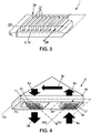
figure 2 est une vue de détail en perspective d'un polariseur linéaire du dispositif de mise en forme d'un faisceau laser de lafigure 1 , comportant un réseau métallique de lames métalliques, - la
figure 3 est une vue de détail en perspective d'une lame à biréfringence de forme du dispositif de mise en forme d'un faisceau laser de lafigure 1 , comportant un réseau diélectrique sub-longueur d'onde d'ordre zéro de lames diélectriques, et - la
figure 4 est un schéma de détail en perspective du dispositif de mise en forme d'un faisceau laser de lafigure 1 , sur lequel est indiqué le trajet d'un faisceau laser comprenant des portions de faisceau laser initial, faisceau laser entrant, faisceau laser interne, faisceau laser sortant et faisceau laser mis en forme.
- the
figure 1 is a cross-sectional diagram of an atomic sensor according to one embodiment of the invention, comprising a device for shaping a laser beam according to one embodiment of the invention, with which are associated a laser d emission of a laser beam as well as a cavity filled with a gas capable of being penetrated by a shaped laser beam and a photodetector for receiving a laser beam having penetrated the cell, - the
picture 2figure 1 , comprising a metal network of metal blades, - the
picture 3figure 1 , comprising a zero-order sub-wavelength dielectric network of dielectric plates, and - the
figure 4 is a perspective detail diagram of the device for shaping a laser beam of thefigure 1 , on which is indicated the path of a laser beam comprising portions of initial laser beam, incoming laser beam, internal laser beam, outgoing laser beam and shaped laser beam.
Sur les différentes figures, les mêmes références désignent des éléments identiques ou similaires.In the various figures, the same references designate identical or similar elements.
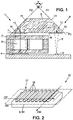
La
Le capteur atomique 1 est par exemple une horloge atomique à l'échelle d'une puce (CSAC pour Chip-Scale Atomic Clock) reposant sur le principe de la résonance atomique par piégeage cohérent de population (CPT pour Coherent Population Trapping).The atomic sensor 1 is for example a chip-scale atomic clock (CSAC for Chip-Scale Atomic Clock) based on the principle of atomic resonance by coherent population trapping (CPT for Coherent Population Trapping).
Dans des variantes de l'invention, le capteur atomique 1 pourrait être un magnétomètre atomique ou un gyromètre atomique par exemple.In variants of the invention, the atomic sensor 1 could be an atomic magnetometer or an atomic gyrometer for example.
La cellule 2 comprend notamment une cavité de gaz 6 munie d'au moins une fenêtre optique 7 et emplie d'un gaz. Le gaz est par exemple un gaz comprenant un élément alcalin en phase vapeur comme du césium ou du rubidium et, le cas échéant un gaz tampon. Le terme « gaz » peut désigner un gaz, une vapeur, ou une vapeur alcaline ou un mélange d'un gaz et d'une vapeur.The
Le capteur atomique 1 comporte par ailleurs un dispositif 8 de mise en forme d'un faisceau laser.The atomic sensor 1 also comprises a
Le dispositif 8 est intercalé, sur le trajet du faisceau laser 5, entre le laser 3 et la cellule 2 et est apte à recevoir un faisceau laser 5 du laser 3 et à transmettre un faisceau laser 5 pénétrant dans la cavité de gaz 6 par la fenêtre optique 7 de la cellule 2.The
Le dispositif 8 de mise en forme comprenant un prisme rétro-réflecteur 9, un polariseur linéaire 10 et une lame à biréfringence de forme 11.The
Comme illustré sur les
Les faces de réflexion 14, 15 forment entre elles un angle droit.The reflection faces 14, 15 form a right angle between them.
Par « les faces forment entre elles un angle droit », on entend que les faces de réflexion 14, 15 s'étendent respectivement selon des plans géométriques d'extension respectifs P1, P2, tels que lesdits plans géométriques d'extension P1, P2 forment un angle droit géométrique l'un avec l'autre.By "the faces form a right angle between them", it is meant that the reflection faces 14, 15 extend respectively along respective geometric extension planes P1, P2, such that said geometric extension planes P1, P2 form a geometric right angle to each other.
Dans l'exemple de réalisation de la
La face de transmission 16 du prisme rétro-réflecteur 9 peut par exemple être orientée à 45° de chacune des faces de réflexion 14, 15.The
Ici également, par « la face de transmission est orientée à 45° de chacune des faces de réflexion 14, 15 », on entend que la face de transmission s'étend selon un plan géométrique d'extension P3 et les faces de réflexion 14, 15 s'étendent respectivement selon des plans géométriques d'extension respectifs P1, P2, tels que le plan géométrique d'extension P3 de la face de transmission forme un angle géométrique de 45° avec chacun des plans géométriques d'extension P1, P2 des faces de réflexion 14, 15.Here also, by "the transmission face is oriented at 45° from each of the reflection faces 14, 15", it is meant that the transmission face extends along a geometric plane of extension P3 and the reflection faces 14, 15 extend respectively along respective geometric extension planes P1, P2, such that the geometric extension plane P3 of the transmission face forms a geometric angle of 45° with each of the geometric extension planes P1, P2 of the transmission face. reflection faces 14, 15.
On remarquera que, autant l'angle entre les faces de réflexion 14, 15 doit être précisément contrôlé pour garantir une rétro-réflexion du faisceau laser, autant l'orientation entre la face de transmission 16 et les faces de réflexion 14, 15 est moins critique car elle implique, au moins pour des angles faibles, principalement un décalage spatial du faisceau et non une erreur angulaire.It will be noted that, as much as the angle between the reflection faces 14, 15 must be precisely controlled to guarantee retro-reflection of the laser beam, as much as the orientation between the
Ainsi, par exemple, l'angle entre les faces de réflexion 14, 15 est avantageusement proche de 90° à ±15 arcsec (±0.004°).Thus, for example, the angle between the reflection faces 14, 15 is advantageously close to 90° at ±15 arcsec (±0.004°).
Le trajet du faisceau laser 5 dans le prisme rétro-réflecteur est illustré sur la
Un faisceau laser entrant 5b pénètre dans le prisme rétro-réflecteur 9 par la zone d'entrée 12 et rencontre une première face de réflexion 14 pour générer un faisceau laser interne 5c. Le faisceau laser interne 5c se propage dans le prisme rétro-réflecteur jusqu'à rencontrer une seconde face de réflexion 15 et générer un faisceau laser sortant 5d quittant le prisme rétro-réflecteur 9 par la zone de sortie 13.An
Le faisceau laser entrant 5b et le faisceau laser sortant 5d sont ainsi parallèles entre eux dans un plan de coupe H du prisme rétro-réflecteur 9.The
Un tel plan de coupe H du prisme rétro-réflecteur 9 est notamment un plan perpendiculaire à direction d'intersection I entre des plans géométriques d'extension P1, P2 respectifs des deux faces de réflexion 14, 15.Such a plane of section H of the retro-reflector prism 9 is in particular a plane perpendicular to the direction of intersection I between respective geometric planes of extension P1, P2 of the two reflection faces 14, 15.
Le prisme rétro-réflecteur peut par exemple être réalisé en un matériau tel que le N-BK7, Sodalime, N-BaK1 ou encore N-SF11.The retro-reflecting prism can for example be made of a material such as N-BK7, Sodalime, N-BaK1 or even N-SF11.
Avantageusement, le prisme rétro-réflecteur peut être réalisé en un matériau présentant un indice de réfraction suffisamment élevé pour garantir une réflexion totale du faisceau laser incident même lorsque celui-ci présente une divergence relative élevée, comme illustré sur la
Le prisme rétro-réflecteur peut être par exemple être réalisé en N-BaK1 caractérisé par un indice de réfraction n=1,564 à une longueur d'onde de 852,1 nm, un tel indice de réfraction garantissant une réflexion totale pour un faisceau laser présentant un angle d'incidence sur la face de transmission 16 compris entre -8° et +8°.The retro-reflecting prism can for example be made of N-BaK1 characterized by a refractive index n=1.564 at a wavelength of 852.1 nm, such a refractive index guaranteeing total reflection for a laser beam having an angle of incidence on the
Le polariseur linéaire 10 est illustré plus en détail sur la
Ce réseau métallique 17 sub-longueur d'onde comporte une pluralité de lames métalliques 18. Les lames métalliques 18 s'étendent parallèlement les unes aux autres selon une direction de lame métallique DM.This sub-wavelength metal grating 17 comprises a plurality of
Les lames métalliques 18 sont par ailleurs juxtaposées les unes par rapport aux autres selon une direction passante DP du réseau métallique 17 perpendiculaire à la direction de lame métalliques DM.The metal strips 18 are also juxtaposed with respect to each other in a passing direction DP of the
Par « réseau sub-longueur d'onde », on entend notamment que les lames métalliques sont juxtaposées les unes par rapport aux autres avec une période spatiale selon la direction passante DP inférieure à la longueur d'onde du faisceau laser 5, sous incidence normale, divisée par l'indice de réfraction du substrat supportant les lames métalliques, par exemple inférieure à environ 900 nm dans le cas d'une horloge atomique au césium.By "sub-wavelength grating" is meant in particular that the metal strips are juxtaposed relative to each other with a spatial period in the passing direction DP less than the wavelength of the
Les lames métalliques 18 sont par exemple réalisées en aluminium ou en or.The
Ainsi, le polariseur linéaire 10 peut par exemple être formé par dépôt d'une couche de matériau métallique sur une plaquette - ou wafer - en verre 19, notamment une couche d'aluminium ou d'or.Thus, the
Dans un exemple de réalisation fourni à titre purement indicatif, le polariseur linéaire 10 est formé par dépôt d'une couche d'aluminium d'une épaisseur de 300 nm mise en forme pour présenter des lames métalliques 18 espacées les unes des autres avec une période de 200 nm et ayant chacune une largeur de 90 nm selon la direction passante du réseau 17, c'est-à-dire présentant un facteur de remplissage (largeur/période) de 0,45.In an exemplary embodiment provided purely for information, the
Dans un autre exemple de réalisation fourni également à titre purement indicatif, le polariseur linéaire 10 est formé par dépôt d'une couche d'or d'une épaisseur de 350 nm mise en forme pour présenter des lames métalliques 18 espacées les unes des autres avec une période de 200 nm et ayant chacune une largeur de 157 nm selon la direction passante du réseau 17, c'est-à-dire présentant un facteur de remplissage (largeur/période) de 0, 45.In another exemplary embodiment also provided purely as an indication, the
D'autres dimensionnements du polariseur linéaire 10, du réseau métallique 17 et des lames métalliques 18 sont bien évidemment envisageables.Other dimensions of the
Le polariseur linéaire 10 est disposé en amont de la zone d'entrée 12 du prisme rétro-réflecteur 9 de sorte à être traversé par un faisceau laser entrant 5b dans le prisme rétro-réflecteur 9 par la zone d'entrée 12. Le polariseur linéaire 10 est apte à imposer une polarisation linéaire audit faisceau laser entrant 5b.The
Plus précisément, le polariseur linéaire 10 reçoit un faisceau laser initial 5a émis par le laser 3 et le transforme en un faisceau laser entrant 5b ayant une polarisation linéaire définie.More precisely, the
En effet, la composante du faisceau laser initial 5a incident qui est parallèle à la direction de lame métalliques DM est convertie en un déplacement d'électrons dans les lames métalliques 18 et donc absorbée par le polariseur linéaire 10, tandis que la composante du faisceau laser initial 5a incident qui est parallèle à la direction passante DP du réseau métallique est laissée intacte dans le faisceau laser entrant 5b.Indeed, the component of the initial
Dans un mode de réalisation particulier de l'invention, le laser 3 d'émission, par exemple un laser à cavité verticale (VCSEL pour Vertical Cavity Surface Emitting Laser), peut comporter un réseau qui garantit l'oscillation sur un seul mode de polarisation, notamment une polarisation linéaire fixée et connue. Dans ce mode de réalisation, le faisceau laser initial 5a peut alors présenter une polarisation linéaire selon une direction de polarisation DL fixée par le laser 3.In a particular embodiment of the invention, the
Il est important de noter que les contraintes d'assemblage du laser 3 dans le capteur atomique 1 rendent très délicat l'alignement précis de cette direction de polarisation DL avec les autres éléments du capteur atomique comme la lame à biréfringence de forme 11, le prisme à réflexion 9 ou encore la cellule optique 2.It is important to note that the assembly constraints of the
Avantageusement, la polarisation linéaire du faisceau laser initial 5a, émis par le laser 3 d'émission, est sensiblement alignée avec la direction passante DP du réseau métallique 17 du polariseur linéaire 10, c'est-à-dire que la direction de polarisation DL et la direction passante DP du réseau métallique sont sensiblement alignées.Advantageously, the linear polarization of the
Par « sensiblement alignée », on entend que les deux directions sont parallèles ou bien proche d'être parallèles, par exemple forment un angle inférieur à 10° entre elles.By “substantially aligned”, it is meant that the two directions are parallel or close to being parallel, for example form an angle of less than 10° between them.
Par ailleurs, le polariseur linéaire 10 est placé en regard de la face de transmission 16 du prisme rétro-réflecteur 9, en étant soit disposé sur ladite face de transmission 16 soit formés sur une plaquette - ou wafer - en verre 19 en contact avec ladite face de transmission 16.Furthermore, the
Comme illustré sur la
La direction passante DP du réseau métallique 17 peut en particulier être parallèle à la direction d'intersection I entre les plans géométrique d'extension P1, P2 des deux faces de réflexion 14, 15.The passing direction DP of the metal grating 17 may in particular be parallel to the direction of intersection I between the geometric extension planes P1, P2 of the two reflection faces 14, 15.
De cette manière, la polarisation linéaire appliquée au faisceau laser entrant 5b est conservée lors des réflexions dans le prisme 9 et donc conservée dans le faisceau laser sortant 5d.In this way, the linear polarization applied to the
Par ailleurs, la lame à biréfringence de forme 11 est illustrée plus en détail sur la
A cette fin, la lame à biréfringence de forme 11 comporte un réseau diélectrique 20 sub-longueur d'onde d'ordre zéro.To this end, the
Ce réseau diélectrique 20 comporte une pluralité de lames diélectriques 21. Les lames diélectriques 21 s'étendent parallèlement les unes aux autres selon une direction de lame diélectrique DD.This
Les lames diélectriques 21 sont par ailleurs juxtaposées les unes par rapport aux autres selon une direction de réseau diélectrique DR perpendiculaire à la direction de lame diélectrique DD.The
Par « réseau sub-longueur d'onde », on entend ici également que les lames diélectriques sont juxtaposées les unes par rapport aux autres avec une période spatiale selon la direction de réseau diélectrique DR inférieure à la longueur d'onde du faisceau laser 5, sous incidence normale, divisée par l'indice de réfraction du substrat supportant les lames diélectriques, par exemple inférieure à environ 900 nm dans le cas d'une horloge atomique au césium.By “sub-wavelength grating”, it is also meant here that the dielectric plates are juxtaposed relative to each other with a spatial period in the direction of the dielectric grating DR less than the wavelength of the
Par « réseau diélectrique d'ordre zéro », en anglais « zero order grating », on entend un réseau diélectrique dont la période séparant les lames diélectriques est suffisamment petite pour que le réseau diélectrique ne génère pas d'ordres de diffraction propagatifs excepté les ordres 0.By “zero order dielectric grating”, in English “zero order grating”, is meant a dielectric grating whose period separating the dielectric blades is sufficiently small for the dielectric grating not to generate propagative diffraction orders except the orders 0.
Un tel réseau diélectrique d'ordre zéro permet de contrôler le déphasage entre la composante transverse électrique et la composante transverse magnétique d'un faisceau laser incident, et donc la polarisation de la lumière sortante en fonction de la polarisation de la lumière entrante.Such a zero-order dielectric network makes it possible to control the phase shift between the transverse electric component and the transverse magnetic component of an incident laser beam, and therefore the polarization of the outgoing light as a function of the polarization of the incoming light.
Les lames diélectriques 21 sont par exemple réalisées en verre ou en nitrure de silicium (Si3N4).The
Ainsi, la lame à biréfringence de forme 11 peut par exemple être formée par dépôt d'une couche de nitrure de silicium (Si3N4) sur une plaquette - ou wafer - en verre 19, par exemple la plaquette - ou wafer - en verre 19 sur laquelle est formé le polariseur linéaire 10.Thus, the
Alternativement, la lame à biréfringence de forme 11 peut être formée en verre (silice), par exemple par gravure d'une plaquette - ou wafer - en verre 19, par exemple la plaquette - ou wafer - en verre 19 sur laquelle est formé le polariseur linéaire 10.Alternatively, the shaped
Dans un exemple de réalisation fourni à titre purement indicatif, la lame à biréfringence de forme 11 est formée par gravure d'une plaquette - ou wafer - en verre 19, mise en forme pour présenter des lames diélectriques 21 d'une épaisseur de 2710 nm espacées les unes des autres avec une période de 580 nm, le réseau diélectrique 20 présentant un facteur de remplissage (largeur/période) de 0,464. Le rapport d'aspect d'un tel réseau (épaisseur/largeur) est donc d'environ 10.In an exemplary embodiment provided purely as an indication, the shaped
Dans un autre exemple de réalisation fourni également à titre purement indicatif, la lame à biréfringence de forme 11 est formée par dépôt d'une couche de nitrure de silicium d'une épaisseur de 598 nm mise en forme pour présenter des lames diélectriques 21 espacées les unes des autres avec une période de 580 nm, le réseau diélectrique 20 présentant un facteur de remplissage (largeur/période) de 0,331. Le rapport d'aspect d'un tel réseau (épaisseur/largeur) est donc d'environ 3.In another exemplary embodiment also provided purely as an indication, the
D'autres dimensionnements de la lame à biréfringence de forme 11, du réseau diélectrique 20 et des lames diélectriques 21 sont bien évidemment envisageables.Other dimensions of the
La lame à biréfringence de forme 11 est disposée en aval de la zone de sortie 13 du prisme rétro-réflecteur 9 de sorte à être traversé par un faisceau laser sortant 5d du prisme rétro-réflecteur 9 par la zone d'entrée 13. La lame à biréfringence de forme 11 est apte à imposer une polarisation circulaire audit faisceau laser sortant 5d pour obtenir un faisceau laser mis en forme 5e.The shaped
Un tel réseau diélectrique d'ordre zéro permet de contrôler le déphasage entre la composante transverse électrique et la composante transverse magnétique d'un faisceau laser incident, et donc la polarisation de la lumière sortante en fonction de la polarisation de la lumière entrante.Such a zero-order dielectric network makes it possible to control the phase shift between the transverse electrical component and the transverse magnetic component of an incident laser beam, and therefore the polarization of the outgoing light as a function of the polarization of the incoming light.
En effet, comme détaillé ci-avant, le réseau diélectrique 20 permet de contrôler le déphasage entre la composante transverse électrique et la composante transverse magnétique d'un faisceau laser incident, et donc la polarisation de la lumière sortante en fonction de la polarisation de la lumière entrante. Le réseau diélectrique 20 se comporte donc comme un matériau anisotrope, où l'anisotropie ne relève pas des propriétés intrinsèque du matériau mais dépend de la structure périodique réalisée à sa surface, qui est suffisamment petite pour manipuler l'indice de réfraction artificiellement.Indeed, as detailed above, the
Les dimensions du réseau diélectrique 20 sont déterminées de sorte à ce que, pour un faisceau sortant 5d ayant une polarisation linéaire, la polarisation du faisceau mis en forme 5e soit circulaire, et par exemple présente une ellipticité de la polarisation circulaire inférieure à 1,1. Les exemples de réseau diélectriques 21 détaillés ci-dessus permettent d'obtenir une telle polarisation.The dimensions of the
Pour adapter les dimensions du réseau diélectrique 20, on peut par exemple mettre en œuvre les équations des théories du milieu effectif (en anglais « EMT »). A ce sujet, il est également fait référence aux indications du document "
Par ailleurs, la lame à biréfringence de forme 11 est placé en regard de la face de transmission 16 du prisme rétro-réflecteur 9, en étant soit disposé sur ladite face de transmission 16 soit formés sur une plaquette - ou wafer - en verre 19 en contact avec ladite face de transmission 16.Furthermore, the shaped
Ainsi par exemple, le polariseur linéaire 10 et la lame à biréfringence de forme 11 peuvent être disposés côte à côte sur la plaquette - ou wafer - en verre 19.Thus, for example, the
Comme illustré sur la
Par ailleurs, le plan géométrique d'extension PL du réseau diélectrique 20 peut être parallèle au plan géométrique d'extension PP du réseau métallique 17.Furthermore, the geometric plane of extension PL of the
Plus particulièrement, la direction de lame diélectrique DD du réseau diélectrique 21 peut former un angle de 45° avec la direction de lame métallique DM.More particularly, the dielectric blade direction DD of the
De manière similaire, étant donné que la direction de réseau diélectrique DR et la direction de lame diélectrique DD du réseau diélectrique 21 sont perpendiculaires, la direction de réseau diélectrique DR peut former un angle de 45° avec la direction de lame métallique DM.Similarly, since the dielectric grating direction DR and the dielectric blade direction DD of the
Ou encore, étant donné que la direction passante DP du réseau métallique et la direction de lame métallique DM du réseau métallique 17 sont perpendiculaires, la direction passante DP du réseau métallique peut former un angle de 45° avec la direction de réseau diélectrique DR ou la direction de lame diélectrique DD.Or, given that the passing direction DP of the metallic grating and the direction of the metallic strip DM of the
De ces manières, le faisceau laser mis en forme 5e peut présenter une polarisation circulaire.In these ways, the 5e-shaped laser beam can exhibit circular polarization.
Claims (12)
- A laser beam (5) shaping device (8) intended in particular to be included in an atomic sensor (1) such as an atomic clock, an atomic magnetometer or an atomic gyrometer by being combined on the one hand with a laser beam (5) emission laser (3) and on the other hand with an alkaline vapour cell (2) comprising a cavity (6) filled with a gas and into which a shaped laser beam (5e) can enter and with a photodetector for receiving (4) a laser beam having entered the cell,wherein the shaping device comprises a retroreflector prism (9) having an entrance area (12) for an entering laser beam (5b), an exit area (13) for an exiting laser beam (5d) as well as two internal laser beam (5c) reflection surfaces (14, 15), said reflection surfaces forming a right angle with one another, a form birefringence plate (11) disposed downstream from the exit area (13) of the retroreflector prism so as to be traversed by an exiting laser beam (5d) exiting the retroreflector prism through the exit area and able to impose a circular polarisation to said exiting laser beam to obtain a shaped laser beam (5e),the shaping device being characterised in that it further comprises a linear polariser (10) disposed upstream from the entrance area (12) of the retroreflector prism (9) so as to be traversed by an entering laser beam (5b) entering the retroreflector prism through the entrance area and able to impose a linear polarisation to said entering laser beam.
- The device according to claim 1, wherein the linear polariser (10) has a sub-wavelength metal network (17), and wherein the sub-wavelength metal network of the linear polariser has a plurality of metal plates (18) extending parallel to each other along a metal plate direction (DM) and being juxtaposed one relative to the other along a passing direction of the metal network (DP) perpendicular to the metal plate direction.
- The device according to claim 2, wherein the passing direction (DP) of the metal network (17) is parallel to a direction of intersection (I) between respective geometric planes of extension (P1, P2) of the two reflection surfaces (14, 15).
- The device according to any one of claims 1 to 3, wherein the form birefringence plate (11) has a zero-order sub-wavelength dielectric network (20), and wherein the zero-order sub-wavelength dielectric network of the form birefringence plate has a plurality of dielectric plates (21) extending parallel to each other along a dielectric plate direction (DD) and being juxtaposed one relative to the other along a dielectric network direction (DR) perpendicular to the dielectric plate direction.
- The device according to claim 4 and any one of claims 2 and 3, wherein the dielectric plate direction (DD) forms an angle of 45° with the metal plate direction (DM).
- The device according to any one of claims 1 to 5, wherein the linear polariser (10) and the form birefringence plate (11) are disposed side-by-side on a glass plate - or wafer (19).
- The device according to any one of claims 1 to 6, wherein the entrance area (12) and the exit area (13) of the retroreflector prism (9) form two portions of a retroreflector prism transmission surface (16) and wherein the linear polariser (10) and the form birefringence plate (11) are placed facing said transmission surface (16), either formed on said transmission surface (16) or formed on a glass plate - or wafer - (19) placed facing said transmission surface (16).
- A method for manufacturing a device (8) for laser beam (5) shaping intended in particular to be included in an atomic sensor (1) such as an atomic clock, an atomic magnetometer or an atomic gyrometer by being combined on the one hand with a laser beam (5) emission laser (3) and on the other hand with an alkaline vapour cell (2) comprising a cavity (6) filled with a gas and into which a shaped laser beam (5e) can enter and with a photodetector for receiving (4) a laser beam having entered the cell, wherein:- a retroreflector prism (9) is available, which has an entrance area (12) for an entering laser beam (5b), an exit area (13) for an exiting laser beam (5d) and two internal laser beam (5c) reflection surfaces (14, 15), said reflection surfaces forming a right angle with one another,- a linear polariser (10) is formed and disposed, which polariser is able to impose a linear polarisation to an entering laser beam (5b) and disposed upstream from the entrance area (12) of the retroreflector prism so as to be traversed by a laser beam entering the retroreflector prism by the entrance area, and- a form birefringence plate (11) is formed and disposed, which plate is able to impose a circular polarisation to an exiting laser beam (5d) and disposed downstream from the exit area (13) of the retroreflector prism so as to be traversed by a laser beam exiting the retroreflector prism by the exit area.
- The method according to claim 8, whereinthe linear polariser (10) is formed by depositing a metal layer on a glass plate -or wafer- (19), in particular an aluminium or gold layer, andthe form birefringence plate (11) is formed on said glass plate - or wafer - (19) either by depositing a layer of dielectric material, in particular a silicon nitride layer, on said glass plate - or wafer - or by etching said glass plate - or wafer -,the linear polariser (10) is disposed upstream from the entrance area (12) of the retroreflector prism and the form birefringence plate (11) downstream from the exit area (13) of the retroreflector prism (9) by placing the glass plate - or wafer - (19) facing a transmission surface (16) of the retroreflector prism (9), wherein the entrance area (12) and the exit area (13) of the retroreflector prism form two portions of said transmission surface (16).
- The method according to claim 8, whereinthe linear polariser (10) is formed and disposed upstream from the entrance area (12) of the retroreflector prism (9) by depositing a layer of metal material, in particular a layer of aluminium or gold, on a transmission surface (16) of the retroreflector prism (9), the entrance area (12) of the retroreflector prism (9) forming a portion of said transmission surface (16), andthe form birefringence plate (11) is formed and deposited downstream from the exit area (13) of the retroreflector prism (9) either by depositing a layer of dielectric material, in particular a layer of silicon nitride, on the transmission surface (16) of the retroreflector prism (9), the exit area (13) of the retroreflector prism forming a portion of said transmission surface (16), or by etching of said transmission surface (16).
- An atomic sensor (1) having a device (8) for shaping a laser beam (5) according to any one of claims 1 to 7, combined, compactly, on the one hand with a laser beam (5) emission laser (3) and on the other hand with an alkaline vapour cell (2) comprising a cavity (6) filled with a gas and into which a shaped laser beam (5e) can enter and a photodetector for receiving (4) a laser beam (5) having entered the cell.
- The atomic sensor according to claim 11, wherein a preferred direction of polarisation (DL) of a laser beam (5) emitted by the emission laser (3) is substantially aligned with the passing direction (DP) of the linear polariser (10) metal network (17).
Applications Claiming Priority (2)
| Application Number | Priority Date | Filing Date | Title |
|---|---|---|---|
| FR1557210A FR3039657B1 (en) | 2015-07-28 | 2015-07-28 | DEVICE FOR FORMING A LASER BEAM FOR AN ATOMIC SENSOR |
| PCT/FR2016/051890 WO2017017351A1 (en) | 2015-07-28 | 2016-07-21 | Device for shaping a laser beam for an atomic sensor |
Publications (2)
| Publication Number | Publication Date |
|---|---|
| EP3329331A1 EP3329331A1 (en) | 2018-06-06 |
| EP3329331B1 true EP3329331B1 (en) | 2022-03-30 |
Family
ID=55542729
Family Applications (1)
| Application Number | Title | Priority Date | Filing Date |
|---|---|---|---|
| EP16757293.2A Active EP3329331B1 (en) | 2015-07-28 | 2016-07-21 | Device for shaping a laser beam for an atomic sensor |
Country Status (6)
| Country | Link |
|---|---|
| US (1) | US11002977B2 (en) |
| EP (1) | EP3329331B1 (en) |
| JP (1) | JP6865733B2 (en) |
| CN (1) | CN108027587B (en) |
| FR (1) | FR3039657B1 (en) |
| WO (1) | WO2017017351A1 (en) |
Families Citing this family (3)
| Publication number | Priority date | Publication date | Assignee | Title |
|---|---|---|---|---|
| CN110260851B (en) * | 2019-05-17 | 2021-07-02 | 北京航空航天大学 | Photodynamic micromechanical gyroscope based on double-sub-wavelength grating cavity detection |
| CN113406876B (en) * | 2021-06-18 | 2022-07-12 | 中国科学院国家授时中心 | Continuous CPT state preparation and differential detection method and system |
| CN116826521B (en) * | 2023-08-31 | 2023-11-28 | 中国航天三江集团有限公司 | Reflective atomic air chamber and preparation method thereof |
Family Cites Families (10)
| Publication number | Priority date | Publication date | Assignee | Title |
|---|---|---|---|---|
| US8164721B2 (en) * | 2003-12-11 | 2012-04-24 | Tan Kim L | Grating trim retarders |
| US7619485B2 (en) * | 2007-01-31 | 2009-11-17 | Teledyne Scientific & Imaging, Llc | Compact optical assembly for chip-scale atomic clock |
| US20110037928A1 (en) * | 2008-05-01 | 2011-02-17 | Little Michael J | Wire grid polarizer for use on the front side oflcds |
| US8816783B2 (en) | 2009-09-04 | 2014-08-26 | Csem Centre Suisse D'electronique Et De Microtechnique S.A. | Device for an atomic clock |
| JP2012074111A (en) * | 2010-09-29 | 2012-04-12 | Toppan Printing Co Ltd | Wide band quarter-wave plate |
| US8624682B2 (en) | 2011-06-13 | 2014-01-07 | Honeywell International Inc. | Vapor cell atomic clock physics package |
| US20130043956A1 (en) * | 2011-08-15 | 2013-02-21 | Honeywell International Inc. | Systems and methods for a nanofabricated optical circular polarizer |
| JP2015082763A (en) * | 2013-10-23 | 2015-04-27 | セイコーエプソン株式会社 | Optical module and atomic oscillator |
| JP6361129B2 (en) * | 2013-12-20 | 2018-07-25 | セイコーエプソン株式会社 | Gas cell, quantum interference device, atomic oscillator, electronic device, and moving object |
| CN105514797B (en) | 2016-01-13 | 2018-07-24 | 山西大学 | Laser frequency lock device and method based on the hyperfine energy level spectrum of two-photon |
-
2015
- 2015-07-28 FR FR1557210A patent/FR3039657B1/en active Active
-
2016
- 2016-07-21 CN CN201680050859.0A patent/CN108027587B/en active Active
- 2016-07-21 WO PCT/FR2016/051890 patent/WO2017017351A1/en active Application Filing
- 2016-07-21 EP EP16757293.2A patent/EP3329331B1/en active Active
- 2016-07-21 US US15/748,563 patent/US11002977B2/en active Active
- 2016-07-21 JP JP2018504219A patent/JP6865733B2/en active Active
Also Published As
| Publication number | Publication date |
|---|---|
| CN108027587B (en) | 2020-07-17 |
| EP3329331A1 (en) | 2018-06-06 |
| WO2017017351A1 (en) | 2017-02-02 |
| US20180217384A1 (en) | 2018-08-02 |
| FR3039657B1 (en) | 2017-08-18 |
| FR3039657A1 (en) | 2017-02-03 |
| CN108027587A (en) | 2018-05-11 |
| US11002977B2 (en) | 2021-05-11 |
| JP2018532133A (en) | 2018-11-01 |
| JP6865733B2 (en) | 2021-04-28 |
Similar Documents
| Publication | Publication Date | Title |
|---|---|---|
| EP2891007B1 (en) | Optical device comprising an optical waveguide and method for manufacturing such a device | |
| EP2906997B1 (en) | Alkali-metal vapour cell, especially for an atomic clock, and manufacturing process | |
| CA1304971C (en) | Dielectric layer polariser | |
| EP3063468B1 (en) | Optical guide suitable for creating two luminous imprints | |
| EP0506546A2 (en) | Optical fiber with Bragg grating and its applications | |
| EP3329331B1 (en) | Device for shaping a laser beam for an atomic sensor | |
| EP3167244B9 (en) | Optical fibre interferometric system | |
| EP2510392B1 (en) | Device for compensating temporaral dispersion applied to ultra-short light pulse generation | |
| EP2284510B1 (en) | Field-compensated static interferometer for Fourier transform spectroscopy | |
| EP0847115A1 (en) | Light amplifier with two incident beams | |
| EP3732531B1 (en) | Optical device possessing means for the precise assembly thereof, assembly or test method for said device | |
| FR2516254A1 (en) | Optical separator for fibre=optic systems - includes bi-reflecting prism with two auxiliary prisms ensuring that transmitted ray is aligned with incident ray | |
| EP3657224B1 (en) | Fixed or variable optical delay line device | |
| FR2975218A1 (en) | Atom cooling and trapping device for use in e.g. rotation sensor, for cooling atoms to specific temperature, has substrate that is made transparent to preset wavelength, and optical beam passing through chip | |
| FR2876448A1 (en) | SOLID STATE GYROLASER STABILIZED WITHOUT BLIND AREA | |
| CA2102593A1 (en) | Interferometric device for determining the characteristics of an integrated optics object | |
| FR2685096A1 (en) | INTEGRATED OPTICAL MIRROR AND METHOD OF MANUFACTURING THE SAME | |
| WO2019102112A1 (en) | Protection of a monostatic or quasi-monostatic laser rangefinder | |
| EP2473824B1 (en) | Field-compensated interferometer | |
| WO2006037932A1 (en) | Optical system with beam propagation extension | |
| FR2856155A1 (en) | Integrated optical circuit for rate gyro, has wave guide that forms Y junction between common guide and two arms, where path difference of light between two arms is greater than coherence length of optical source | |
| FR2645261A1 (en) | MIXING AND READING DEVICE FOR A LASER GYROMETER |
Legal Events
| Date | Code | Title | Description |
|---|---|---|---|
| STAA | Information on the status of an ep patent application or granted ep patent |
Free format text: STATUS: THE INTERNATIONAL PUBLICATION HAS BEEN MADE |
|
| PUAI | Public reference made under article 153(3) epc to a published international application that has entered the european phase |
Free format text: ORIGINAL CODE: 0009012 |
|
| STAA | Information on the status of an ep patent application or granted ep patent |
Free format text: STATUS: REQUEST FOR EXAMINATION WAS MADE |
|
| 17P | Request for examination filed |
Effective date: 20180202 |
|
| AK | Designated contracting states |
Kind code of ref document: A1 Designated state(s): AL AT BE BG CH CY CZ DE DK EE ES FI FR GB GR HR HU IE IS IT LI LT LU LV MC MK MT NL NO PL PT RO RS SE SI SK SM TR |
|
| AX | Request for extension of the european patent |
Extension state: BA ME |
|
| DAV | Request for validation of the european patent (deleted) | ||
| DAX | Request for extension of the european patent (deleted) | ||
| GRAP | Despatch of communication of intention to grant a patent |
Free format text: ORIGINAL CODE: EPIDOSNIGR1 |
|
| STAA | Information on the status of an ep patent application or granted ep patent |
Free format text: STATUS: GRANT OF PATENT IS INTENDED |
|
| INTG | Intention to grant announced |
Effective date: 20211029 |
|
| GRAS | Grant fee paid |
Free format text: ORIGINAL CODE: EPIDOSNIGR3 |
|
| GRAA | (expected) grant |
Free format text: ORIGINAL CODE: 0009210 |
|
| STAA | Information on the status of an ep patent application or granted ep patent |
Free format text: STATUS: THE PATENT HAS BEEN GRANTED |
|
| AK | Designated contracting states |
Kind code of ref document: B1 Designated state(s): AL AT BE BG CH CY CZ DE DK EE ES FI FR GB GR HR HU IE IS IT LI LT LU LV MC MK MT NL NO PL PT RO RS SE SI SK SM TR |
|
| REG | Reference to a national code |
Ref country code: GB Ref legal event code: FG4D Free format text: NOT ENGLISH |
|
| REG | Reference to a national code |
Ref country code: CH Ref legal event code: EP |
|
| REG | Reference to a national code |
Ref country code: AT Ref legal event code: REF Ref document number: 1479766 Country of ref document: AT Kind code of ref document: T Effective date: 20220415 |
|
| REG | Reference to a national code |
Ref country code: DE Ref legal event code: R096 Ref document number: 602016070517 Country of ref document: DE |
|
| REG | Reference to a national code |
Ref country code: IE Ref legal event code: FG4D Free format text: LANGUAGE OF EP DOCUMENT: FRENCH |
|
| REG | Reference to a national code |
Ref country code: LT Ref legal event code: MG9D |
|
| PG25 | Lapsed in a contracting state [announced via postgrant information from national office to epo] |
Ref country code: SE Free format text: LAPSE BECAUSE OF FAILURE TO SUBMIT A TRANSLATION OF THE DESCRIPTION OR TO PAY THE FEE WITHIN THE PRESCRIBED TIME-LIMIT Effective date: 20220330 Ref country code: RS Free format text: LAPSE BECAUSE OF FAILURE TO SUBMIT A TRANSLATION OF THE DESCRIPTION OR TO PAY THE FEE WITHIN THE PRESCRIBED TIME-LIMIT Effective date: 20220330 Ref country code: NO Free format text: LAPSE BECAUSE OF FAILURE TO SUBMIT A TRANSLATION OF THE DESCRIPTION OR TO PAY THE FEE WITHIN THE PRESCRIBED TIME-LIMIT Effective date: 20220630 Ref country code: LT Free format text: LAPSE BECAUSE OF FAILURE TO SUBMIT A TRANSLATION OF THE DESCRIPTION OR TO PAY THE FEE WITHIN THE PRESCRIBED TIME-LIMIT Effective date: 20220330 Ref country code: HR Free format text: LAPSE BECAUSE OF FAILURE TO SUBMIT A TRANSLATION OF THE DESCRIPTION OR TO PAY THE FEE WITHIN THE PRESCRIBED TIME-LIMIT Effective date: 20220330 Ref country code: BG Free format text: LAPSE BECAUSE OF FAILURE TO SUBMIT A TRANSLATION OF THE DESCRIPTION OR TO PAY THE FEE WITHIN THE PRESCRIBED TIME-LIMIT Effective date: 20220630 |
|
| REG | Reference to a national code |
Ref country code: NL Ref legal event code: MP Effective date: 20220330 |
|
| REG | Reference to a national code |
Ref country code: AT Ref legal event code: MK05 Ref document number: 1479766 Country of ref document: AT Kind code of ref document: T Effective date: 20220330 |
|
| PG25 | Lapsed in a contracting state [announced via postgrant information from national office to epo] |
Ref country code: LV Free format text: LAPSE BECAUSE OF FAILURE TO SUBMIT A TRANSLATION OF THE DESCRIPTION OR TO PAY THE FEE WITHIN THE PRESCRIBED TIME-LIMIT Effective date: 20220330 Ref country code: GR Free format text: LAPSE BECAUSE OF FAILURE TO SUBMIT A TRANSLATION OF THE DESCRIPTION OR TO PAY THE FEE WITHIN THE PRESCRIBED TIME-LIMIT Effective date: 20220701 Ref country code: FI Free format text: LAPSE BECAUSE OF FAILURE TO SUBMIT A TRANSLATION OF THE DESCRIPTION OR TO PAY THE FEE WITHIN THE PRESCRIBED TIME-LIMIT Effective date: 20220330 |
|
| PG25 | Lapsed in a contracting state [announced via postgrant information from national office to epo] |
Ref country code: NL Free format text: LAPSE BECAUSE OF FAILURE TO SUBMIT A TRANSLATION OF THE DESCRIPTION OR TO PAY THE FEE WITHIN THE PRESCRIBED TIME-LIMIT Effective date: 20220330 |
|
| PG25 | Lapsed in a contracting state [announced via postgrant information from national office to epo] |
Ref country code: SM Free format text: LAPSE BECAUSE OF FAILURE TO SUBMIT A TRANSLATION OF THE DESCRIPTION OR TO PAY THE FEE WITHIN THE PRESCRIBED TIME-LIMIT Effective date: 20220330 Ref country code: SK Free format text: LAPSE BECAUSE OF FAILURE TO SUBMIT A TRANSLATION OF THE DESCRIPTION OR TO PAY THE FEE WITHIN THE PRESCRIBED TIME-LIMIT Effective date: 20220330 Ref country code: RO Free format text: LAPSE BECAUSE OF FAILURE TO SUBMIT A TRANSLATION OF THE DESCRIPTION OR TO PAY THE FEE WITHIN THE PRESCRIBED TIME-LIMIT Effective date: 20220330 Ref country code: PT Free format text: LAPSE BECAUSE OF FAILURE TO SUBMIT A TRANSLATION OF THE DESCRIPTION OR TO PAY THE FEE WITHIN THE PRESCRIBED TIME-LIMIT Effective date: 20220801 Ref country code: ES Free format text: LAPSE BECAUSE OF FAILURE TO SUBMIT A TRANSLATION OF THE DESCRIPTION OR TO PAY THE FEE WITHIN THE PRESCRIBED TIME-LIMIT Effective date: 20220330 Ref country code: EE Free format text: LAPSE BECAUSE OF FAILURE TO SUBMIT A TRANSLATION OF THE DESCRIPTION OR TO PAY THE FEE WITHIN THE PRESCRIBED TIME-LIMIT Effective date: 20220330 Ref country code: CZ Free format text: LAPSE BECAUSE OF FAILURE TO SUBMIT A TRANSLATION OF THE DESCRIPTION OR TO PAY THE FEE WITHIN THE PRESCRIBED TIME-LIMIT Effective date: 20220330 Ref country code: AT Free format text: LAPSE BECAUSE OF FAILURE TO SUBMIT A TRANSLATION OF THE DESCRIPTION OR TO PAY THE FEE WITHIN THE PRESCRIBED TIME-LIMIT Effective date: 20220330 |
|
| PG25 | Lapsed in a contracting state [announced via postgrant information from national office to epo] |
Ref country code: PL Free format text: LAPSE BECAUSE OF FAILURE TO SUBMIT A TRANSLATION OF THE DESCRIPTION OR TO PAY THE FEE WITHIN THE PRESCRIBED TIME-LIMIT Effective date: 20220330 Ref country code: IS Free format text: LAPSE BECAUSE OF FAILURE TO SUBMIT A TRANSLATION OF THE DESCRIPTION OR TO PAY THE FEE WITHIN THE PRESCRIBED TIME-LIMIT Effective date: 20220730 Ref country code: AL Free format text: LAPSE BECAUSE OF FAILURE TO SUBMIT A TRANSLATION OF THE DESCRIPTION OR TO PAY THE FEE WITHIN THE PRESCRIBED TIME-LIMIT Effective date: 20220330 |
|
| REG | Reference to a national code |
Ref country code: DE Ref legal event code: R097 Ref document number: 602016070517 Country of ref document: DE |
|
| PG25 | Lapsed in a contracting state [announced via postgrant information from national office to epo] |
Ref country code: DK Free format text: LAPSE BECAUSE OF FAILURE TO SUBMIT A TRANSLATION OF THE DESCRIPTION OR TO PAY THE FEE WITHIN THE PRESCRIBED TIME-LIMIT Effective date: 20220330 |
|
| PLBE | No opposition filed within time limit |
Free format text: ORIGINAL CODE: 0009261 |
|
| STAA | Information on the status of an ep patent application or granted ep patent |
Free format text: STATUS: NO OPPOSITION FILED WITHIN TIME LIMIT |
|
| PG25 | Lapsed in a contracting state [announced via postgrant information from national office to epo] |
Ref country code: MC Free format text: LAPSE BECAUSE OF FAILURE TO SUBMIT A TRANSLATION OF THE DESCRIPTION OR TO PAY THE FEE WITHIN THE PRESCRIBED TIME-LIMIT Effective date: 20220330 |
|
| 26N | No opposition filed |
Effective date: 20230103 |
|
| REG | Reference to a national code |
Ref country code: BE Ref legal event code: MM Effective date: 20220731 |
|
| PG25 | Lapsed in a contracting state [announced via postgrant information from national office to epo] |
Ref country code: LU Free format text: LAPSE BECAUSE OF NON-PAYMENT OF DUE FEES Effective date: 20220721 |
|
| PG25 | Lapsed in a contracting state [announced via postgrant information from national office to epo] |
Ref country code: SI Free format text: LAPSE BECAUSE OF FAILURE TO SUBMIT A TRANSLATION OF THE DESCRIPTION OR TO PAY THE FEE WITHIN THE PRESCRIBED TIME-LIMIT Effective date: 20220330 Ref country code: BE Free format text: LAPSE BECAUSE OF NON-PAYMENT OF DUE FEES Effective date: 20220731 |
|
| PG25 | Lapsed in a contracting state [announced via postgrant information from national office to epo] |
Ref country code: IT Free format text: LAPSE BECAUSE OF FAILURE TO SUBMIT A TRANSLATION OF THE DESCRIPTION OR TO PAY THE FEE WITHIN THE PRESCRIBED TIME-LIMIT Effective date: 20220330 Ref country code: IE Free format text: LAPSE BECAUSE OF NON-PAYMENT OF DUE FEES Effective date: 20220721 |
|
| PGFP | Annual fee paid to national office [announced via postgrant information from national office to epo] |
Ref country code: GB Payment date: 20230725 Year of fee payment: 8 Ref country code: CH Payment date: 20230801 Year of fee payment: 8 |
|
| PGFP | Annual fee paid to national office [announced via postgrant information from national office to epo] |
Ref country code: FR Payment date: 20230727 Year of fee payment: 8 Ref country code: DE Payment date: 20230712 Year of fee payment: 8 |
|
| PG25 | Lapsed in a contracting state [announced via postgrant information from national office to epo] |
Ref country code: HU Free format text: LAPSE BECAUSE OF FAILURE TO SUBMIT A TRANSLATION OF THE DESCRIPTION OR TO PAY THE FEE WITHIN THE PRESCRIBED TIME-LIMIT; INVALID AB INITIO Effective date: 20160721 |