EP3329331B1 - Vorrichtung zur formung eines laserstrahls für einen atomsensor - Google Patents
Vorrichtung zur formung eines laserstrahls für einen atomsensor Download PDFInfo
- Publication number
- EP3329331B1 EP3329331B1 EP16757293.2A EP16757293A EP3329331B1 EP 3329331 B1 EP3329331 B1 EP 3329331B1 EP 16757293 A EP16757293 A EP 16757293A EP 3329331 B1 EP3329331 B1 EP 3329331B1
- Authority
- EP
- European Patent Office
- Prior art keywords
- laser beam
- retroreflector prism
- plate
- dielectric
- atomic
- Prior art date
- Legal status (The legal status is an assumption and is not a legal conclusion. Google has not performed a legal analysis and makes no representation as to the accuracy of the status listed.)
- Active
Links
Images
Classifications
-
- G—PHYSICS
- G02—OPTICS
- G02B—OPTICAL ELEMENTS, SYSTEMS OR APPARATUS
- G02B27/00—Optical systems or apparatus not provided for by any of the groups G02B1/00 - G02B26/00, G02B30/00
- G02B27/09—Beam shaping, e.g. changing the cross-sectional area, not otherwise provided for
- G02B27/0938—Using specific optical elements
- G02B27/095—Refractive optical elements
- G02B27/0972—Prisms
-
- G—PHYSICS
- G02—OPTICS
- G02B—OPTICAL ELEMENTS, SYSTEMS OR APPARATUS
- G02B27/00—Optical systems or apparatus not provided for by any of the groups G02B1/00 - G02B26/00, G02B30/00
- G02B27/28—Optical systems or apparatus not provided for by any of the groups G02B1/00 - G02B26/00, G02B30/00 for polarising
-
- G—PHYSICS
- G02—OPTICS
- G02B—OPTICAL ELEMENTS, SYSTEMS OR APPARATUS
- G02B5/00—Optical elements other than lenses
- G02B5/04—Prisms
-
- G—PHYSICS
- G02—OPTICS
- G02B—OPTICAL ELEMENTS, SYSTEMS OR APPARATUS
- G02B5/00—Optical elements other than lenses
- G02B5/12—Reflex reflectors
- G02B5/122—Reflex reflectors cube corner, trihedral or triple reflector type
-
- G—PHYSICS
- G02—OPTICS
- G02B—OPTICAL ELEMENTS, SYSTEMS OR APPARATUS
- G02B5/00—Optical elements other than lenses
- G02B5/30—Polarising elements
- G02B5/3025—Polarisers, i.e. arrangements capable of producing a definite output polarisation state from an unpolarised input state
- G02B5/3058—Polarisers, i.e. arrangements capable of producing a definite output polarisation state from an unpolarised input state comprising electrically conductive elements, e.g. wire grids, conductive particles
-
- G—PHYSICS
- G02—OPTICS
- G02B—OPTICAL ELEMENTS, SYSTEMS OR APPARATUS
- G02B5/00—Optical elements other than lenses
- G02B5/30—Polarising elements
- G02B5/3083—Birefringent or phase retarding elements
-
- G—PHYSICS
- G04—HOROLOGY
- G04F—TIME-INTERVAL MEASURING
- G04F5/00—Apparatus for producing preselected time intervals for use as timing standards
- G04F5/14—Apparatus for producing preselected time intervals for use as timing standards using atomic clocks
- G04F5/145—Apparatus for producing preselected time intervals for use as timing standards using atomic clocks using Coherent Population Trapping
Definitions
- the invention relates to the field of atomic sensors comprising alkaline vapor cells and laser beam shaping devices as well as laser beam shaping devices for such atomic sensors.
- a typical atomic sensor according to the invention is a chip-scale atomic clock, known by the acronym CSAC (for Chip-Scale Atomic Clock).
- CSAC Chip-Scale Atomic Clock
- An example is the CSAC called SA.45s from the company MICROSEMI which has a volume of 16 cm3, a mass of 35 g and requires a power of only 120 mW.
- Such an atomic micro-clock is also known from the work of the MAC-TFC consortium, the FEMTO-ST institute (acronym for Franche-Comté Electronique Mécanique Thermique et Optique - Sciences et Technologies) which has developed a very compact cesium vapor cell (a few mm3), with micro-machining MEMS (acronym for MicroElectroMechanical Systems) of the silicon and anodic welding (see for example “New approach of fabrication and dispensing of micromachined cesium vapor cell” by L. Nieradko, C. Gorecki, A. Douahi, V. Giordano, JC Beugnot, J. Dziuban and M. Moraja published in JOURNAL OF MICRO-NANOLITHOGRAPHY MEMS AND MOEMS August 2008 ).
- Such a cell has an optical window diameter of approximately 2 millimeters.
- the beam from such a vertical cavity laser is characterized by relatively low divergence (FWHM 10-15°) and size (about 20 microns at the output mirror).
- the invention finally relates to an atomic sensor comprising a device for shaping a laser beam as defined in claim 11.
- the dependent claims define additional embodiments.
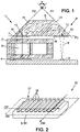
- the retro-reflecting prism 9 comprises an entry zone 12 for an incoming laser beam 5b, an exit zone 13 for an outgoing laser beam 5d as well as two reflection faces 14, 15 for an internal laser beam 5c .
- Such a plane of section H of the retro-reflector prism 9 is in particular a plane perpendicular to the direction of intersection I between respective geometric planes of extension P1, P2 of the two reflection faces 14, 15.
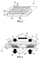
- the metal strips 18 are also juxtaposed with respect to each other in a passing direction DP of the metal network 17 perpendicular to the direction of the metal strip DM.
- the geometric plane of extension PL of the dielectric network 20 can be parallel to the geometric plane of extension PP of the metal network 17.
Landscapes
- Physics & Mathematics (AREA)
- General Physics & Mathematics (AREA)
- Optics & Photonics (AREA)
- Life Sciences & Earth Sciences (AREA)
- Ecology (AREA)
- Investigating Or Analysing Materials By Optical Means (AREA)
- Polarising Elements (AREA)
Claims (12)
- Vorrichtung (8) zur Formung eines Laserstrahls (5), insbesondere dafür gedacht, in einem Atomsensor (1), wie einer Atomuhr, einem Atommagnetometer oder einem Atomgyrometer, enthalten zu sein, indem sie einerseits einem Emissionslaser (3) eines Laserstrahls (5) und andererseits einer Alkalidampfzelle (2), die einen Hohlraum (6) umfasst, der mit einem Gas gefüllt ist und in den ein geformter Laserstrahl (5e) eindringen kann, und einem Fotoempfänger (4) zum Empfangen eines Laserstrahls, der in die Zelle eingedrungen ist, zugeordnet wird,wobei die Vorrichtung zur Formung ein Retroreflektorprisma (9) umfasst, das einen Eintrittsbereich (12) für einen eintretenden Laserstrahl (5b), einen Austrittsbereich (13) für einen austretenden Laserstrahl (5d) sowie zwei Reflexionsflächen (14, 15) für einen internen Laserstrahl (5c) aufweist, wobei die Reflexionsflächen zwischen sich einen rechten Winkel bilden, eine Formdoppelbrechungslamelle (11) derart stromabwärts des Austrittsbereichs (13) des Retroreflektorprismas angeordnet ist, dass sie von einem durch den Austrittsbereich aus dem Retroreflektorprisma austretenden Laserstrahl (5d) gequert wird und den austretenden Laserstrahl in eine kreisförmige Polarisation bringen kann, um einen geformten Laserstrahl (5e) zu erhalten,wobei die Vorrichtung zur Formung dadurch gekennzeichnet ist, dass sie ferner einen linearen Polarisator (10) umfasst, der derart stromaufwärts des Eintrittsbereichs (12) des Retroreflektorprismas (9) angeordnet ist, dass er von einem durch den Eintrittsbereich in das Retroreflektorprisma eintretenden Laserstrahl (5b) gequert wird und den eintretenden Laserstrahl in eine lineare Polarisation bringen kann.
- Vorrichtung nach Anspruch 1, wobei der lineare Polarisator (10) ein metallisches Subwellenlängengitter (17) aufweist und wobei das metallische Subwellenlängengitter des linearen Polarisators eine Vielzahl von Metalllamellen (18) aufweist, die sich entlang einer Richtung der Metalllamelle (DM) parallel zueinander erstrecken und entlang einer Durchgangsrichtung des Metallgitters (DP) senkrecht zur Richtung der Metalllamelle nebeneinander angeordnet sind.
- Vorrichtung nach Anspruch 2, wobei die Durchgangsrichtung (DP) des Metallgitters (17) parallel zu einer Überschneidungsrichtung (I) zwischen den jeweiligen geometrischen Erstreckungsebenen (P1, P2) der zwei Reflexionsflächen (14, 15) liegt.
- Vorrichtung nach einem der Ansprüche 1 bis 3, wobei die Formdoppelbrechungslamelle (11) ein dielektrisches Subwellenlängengitter (20) mit der Zahl Null aufweist und wobei das dielektrische Subwellenlängengitter mit der Zahl Null der Formdoppelbrechungslamelle eine Vielzahl von dielektrischen Lamellen (21) aufweist, die sich entlang einer Richtung der dielektrischen Lamelle (DD) parallel zueinander erstrecken und entlang einer Richtung des dielektrischen Gitters (DR) senkrecht zur Richtung der dielektrischen Lamelle nebeneinander angeordnet sind.
- Vorrichtung nach Anspruch 4 und einem der Ansprüche 2 bis 3, wobei die Richtung der dielektrischen Lamelle (DD) einen Winkel von 45° mit der Richtung der Metalllamelle (DM) bildet.
- Vorrichtung nach einem der Ansprüche 1 bis 5, wobei der lineare Polarisator (10) und die Formdoppelbrechungslamelle (11) nebeneinander auf einer Leiterplatte - oder einem Wafer - aus Glas (19) angeordnet sind.
- Vorrichtung nach einem der Ansprüche 1 bis 6, wobei der Eintrittsbereich (12) und der Austrittsbereich (13) des Retroreflektorprismas (9) zwei Abschnitte einer Transmissionsfläche (16) des Retroreflektorprismas bilden und wobei der lineare Polarisator (10) und die Formdoppelbrechungslamelle (11) gegenüber der Transmissionsfläche (16) platziert sind, wobei sie entweder auf der Transmissionsfläche (16) oder auf einer Leiterplatte - oder einem Wafer - aus Glas (19) gebildet sind, die bzw. der gegenüber der Transmissionsfläche (16) platziert ist.
- Herstellungsverfahren für eine Vorrichtung (8) zur Formung eines Laserstrahls (5), insbesondere dafür gedacht, in einem Atomsensor (1), wie einer Atomuhr, einem Atommagnetometer oder einem Atomgyrometer, enthalten zu sein, indem sie einerseits einem Emissionslaser (3) eines Laserstrahls (5) und andererseits einer Alkalidampfzelle (2), die einen Hohlraum (6) umfasst, der mit einem Gas gefüllt ist, und in den ein geformter Laserstrahl (5e) eindringen kann, und einem Fotoempfänger (4) zum Empfangen eines Laserstrahls, der in die Zelle eingedrungen ist, zugeordnet wird, wobei:- ein Retroreflektorprisma (9) vorhanden ist, das einen Eintrittsbereich (12) für einen eintretenden Laserstrahl (5b), einen Austrittsbereich (13) für einen austretenden Laserstrahl (5d) sowie zwei Reflexionsflächen (14, 15) für einen internen Laserstrahl (5c) aufweist, wobei die Reflexionsflächen zwischen sich einen rechten Winkel bilden,- ein linearer Polarisator (10) gebildet und angeordnet wird, der einen eintretenden Laserstrahl (5b) in eine lineare Polarisation bringen kann, und der stromaufwärts des Eintrittsbereichs (12) des Retroreflektorprismas angeordnet ist, so dass er von einem durch den Eintrittsbereich in das Retroreflektorprisma eintretenden Laserstrahl gequert wird, und- eine Formdoppelbrechungslamelle (11) gebildet und angeordnet wird, die einen austretenden Laserstrahl (5d) in eine kreisförmige Polarisation bringen kann, und die stromabwärts des Austrittsbereichs (13) des Retroreflektorprismas angeordnet ist, so dass sie von einem durch den Austrittsbereich aus dem Retroreflektorprisma austretenden Laserstrahl gequert wird.
- Verfahren nach Anspruch 8, wobeider lineare Polarisator (10) durch Ablagern einer Schicht aus metallischem Material auf einer Leiterplatte - oder einem Wafer - aus Glas (19), insbesondere einer Aluminium- oder Goldschicht, gebildet wird, unddie Formdoppelbrechungslamelle (11) auf der Leiterplatte - oder dem Wafer - aus Glas (19) entweder durch Ablagern einer Schicht aus dielektrischem Material, insbesondere einer Siliciumnitridschicht, auf der Leiterplatte - oder dem Wafer - aus Glas oder durch Gravieren der Leiterplatte - oder des Wafers - aus Glas gebildet wird,der lineare Polarisator (10) stromaufwärts des Eintrittsbereichs (12) des Retroreflektorprismas und die Formdoppelbrechungslamelle (11) stromabwärts des Austrittsbereichs (13) des Retroreflektorprismas (9) angeordnet werden, indem die Leiterplatte - oder der Wafer - aus Glas (19) gegenüber einer Transmissionsfläche (16) des Retroreflektorprismas (9) platziert werden, wobei der Eintrittsbereich (12) und der Austrittsbereich (13) des Retroreflektorprismas zwei Abschnitte der Transmissionsfläche (16) bilden.
- Verfahren nach Anspruch 8, wobeider lineare Polarisator (10) stromaufwärts des Eintrittsbereichs (12) des Retroreflektorprismas (9) durch Ablagern einer Schicht aus metallischem Material, insbesondere einer Aluminium- oder Goldschicht, auf einer Transmissionsfläche (16) des Retroreflektorprismas (9) gebildet und angeordnet wird, wobei der Eintrittsbereich (12) des Retroreflektorprismas (9) einen Abschnitt der Transmissionsfläche (16) bildet, unddie Formdoppelbrechungslamelle (11) stromabwärts des Austrittsbereichs (13) des Retroreflektorprismas (9) entweder durch Ablagern einer Schicht aus dielektrischem Material, insbesondere einer Siliciumnitridschicht, auf der Transmissionsfläche (16) des Retroreflektorprismas (9), wobei der Austrittsbereich (13) des Retroreflektorprismas einen Abschnitt der Transmissionsfläche (16) bildet, oder durch Gravieren der Transmissionsfläche (16) gebildet und angeordnet wird.
- Atomsensor (1), aufweisend eine Vorrichtung (8) zur Formung eines Laserstrahls (5) nach einem der Ansprüche 1 bis 7, die in kompakter Weise einerseits einem Emissionslaser (3) eines Laserstrahls (5) und andererseits einer Alkalidampfzelle (2), die einen Hohlraum (6) umfasst, der mit einem Gas gefüllt ist, und in den ein geformter Laserstrahl (5e) eindringen kann, und einem Fotoempfänger (4) zum Empfangen eines Laserstrahls (5), der in die Zelle eingedrungen ist, zugeordnet ist,
- Atomsensor (1) nach Anspruch 11, wobei eine bevorzugte Polarisationsrichtung (DL) eines Laserstrahls (5), der von dem Emissionslaser (3) ausgestrahlt wird, im Wesentlichen mit der Durchgangsrichtung (DP) des Metallgitters (17) des linearen Polarisators (10) ausgerichtet ist.
Applications Claiming Priority (2)
| Application Number | Priority Date | Filing Date | Title |
|---|---|---|---|
| FR1557210A FR3039657B1 (fr) | 2015-07-28 | 2015-07-28 | Dispositif de mise en forme d'un faisceau laser pour un capteur atomique |
| PCT/FR2016/051890 WO2017017351A1 (fr) | 2015-07-28 | 2016-07-21 | Dispositif de mise en forme d'un faisceau laser pour un capteur atomique |
Publications (2)
| Publication Number | Publication Date |
|---|---|
| EP3329331A1 EP3329331A1 (de) | 2018-06-06 |
| EP3329331B1 true EP3329331B1 (de) | 2022-03-30 |
Family
ID=55542729
Family Applications (1)
| Application Number | Title | Priority Date | Filing Date |
|---|---|---|---|
| EP16757293.2A Active EP3329331B1 (de) | 2015-07-28 | 2016-07-21 | Vorrichtung zur formung eines laserstrahls für einen atomsensor |
Country Status (6)
| Country | Link |
|---|---|
| US (1) | US11002977B2 (de) |
| EP (1) | EP3329331B1 (de) |
| JP (1) | JP6865733B2 (de) |
| CN (1) | CN108027587B (de) |
| FR (1) | FR3039657B1 (de) |
| WO (1) | WO2017017351A1 (de) |
Families Citing this family (3)
| Publication number | Priority date | Publication date | Assignee | Title |
|---|---|---|---|---|
| CN110260851B (zh) * | 2019-05-17 | 2021-07-02 | 北京航空航天大学 | 一种基于双亚波长光栅腔检测的光力学微机械陀螺 |
| CN113406876B (zh) * | 2021-06-18 | 2022-07-12 | 中国科学院国家授时中心 | 连续式cpt态制备与差分探测的方法及系统 |
| CN116826521B (zh) * | 2023-08-31 | 2023-11-28 | 中国航天三江集团有限公司 | 一种反射式原子气室及其制备方法 |
Family Cites Families (10)
| Publication number | Priority date | Publication date | Assignee | Title |
|---|---|---|---|---|
| US8164721B2 (en) * | 2003-12-11 | 2012-04-24 | Tan Kim L | Grating trim retarders |
| US7619485B2 (en) * | 2007-01-31 | 2009-11-17 | Teledyne Scientific & Imaging, Llc | Compact optical assembly for chip-scale atomic clock |
| WO2009134269A1 (en) * | 2008-05-01 | 2009-11-05 | Agoura Technologies, Inc. | A wire grid polarizer for use on the front side of lcds |
| EP2473885B1 (de) * | 2009-09-04 | 2013-05-29 | CSEM Centre Suisse D'electronique Et De Microtechnique SA | Vorrichtung für atomuhr |
| JP2012074111A (ja) * | 2010-09-29 | 2012-04-12 | Toppan Printing Co Ltd | 広帯域1/4波長板 |
| US8624682B2 (en) * | 2011-06-13 | 2014-01-07 | Honeywell International Inc. | Vapor cell atomic clock physics package |
| US20130043956A1 (en) * | 2011-08-15 | 2013-02-21 | Honeywell International Inc. | Systems and methods for a nanofabricated optical circular polarizer |
| JP2015082763A (ja) * | 2013-10-23 | 2015-04-27 | セイコーエプソン株式会社 | 光学モジュールおよび原子発振器 |
| JP6361129B2 (ja) * | 2013-12-20 | 2018-07-25 | セイコーエプソン株式会社 | ガスセル、量子干渉装置、原子発振器、電子機器および移動体 |
| CN105514797B (zh) * | 2016-01-13 | 2018-07-24 | 山西大学 | 基于双光子超精细能级光谱的激光频率锁定装置及方法 |
-
2015
- 2015-07-28 FR FR1557210A patent/FR3039657B1/fr active Active
-
2016
- 2016-07-21 EP EP16757293.2A patent/EP3329331B1/de active Active
- 2016-07-21 CN CN201680050859.0A patent/CN108027587B/zh active Active
- 2016-07-21 US US15/748,563 patent/US11002977B2/en active Active
- 2016-07-21 JP JP2018504219A patent/JP6865733B2/ja active Active
- 2016-07-21 WO PCT/FR2016/051890 patent/WO2017017351A1/fr not_active Ceased
Also Published As
| Publication number | Publication date |
|---|---|
| CN108027587A (zh) | 2018-05-11 |
| US20180217384A1 (en) | 2018-08-02 |
| FR3039657B1 (fr) | 2017-08-18 |
| FR3039657A1 (fr) | 2017-02-03 |
| CN108027587B (zh) | 2020-07-17 |
| WO2017017351A1 (fr) | 2017-02-02 |
| JP2018532133A (ja) | 2018-11-01 |
| US11002977B2 (en) | 2021-05-11 |
| JP6865733B2 (ja) | 2021-04-28 |
| EP3329331A1 (de) | 2018-06-06 |
Similar Documents
| Publication | Publication Date | Title |
|---|---|---|
| EP2891007B1 (de) | Optische vorrichtung mit einem lichtwellenleiter und verfahren zur herstellung einer solchen vorrichtung | |
| EP2906997B1 (de) | Alkalimetalldampfzelle, insbesondere für eine atomuhr, und herstellungsverfahren | |
| CA1304971C (fr) | Polariseur a couches dielectriques | |
| EP3063468B1 (de) | Optischer leiter zur erzeugung zwei leuchtender prägungen | |
| EP0506546A2 (de) | Optischer Faser mit Bragg-Gitter und ihre Anwendungen | |
| EP3329331B1 (de) | Vorrichtung zur formung eines laserstrahls für einen atomsensor | |
| EP2284510B1 (de) | Statischer Interferometer mit kompensiertem Feld für die Fourier-Transform-Spektrometrie | |
| EP3732531B1 (de) | Optische vorrichtung mit mitteln zur präzisen montage derselben, anordnung oder testverfahren für diese vorrichtung | |
| EP0847115A1 (de) | Lichtverstärkervorrichtung mit zwei einfallenden Bündeln | |
| FR2953945A1 (fr) | Dispositif pour la compensation de la dispersion temporelle appliquee a la generation d'impulsions lumineuses ultra breves. | |
| FR2516254A1 (fr) | Separateur optique pour la separation ou la superposition de deux faisceaux de lumiere | |
| WO2024126592A1 (fr) | Dispositif optique dispersif et système laser à impulsions brèves comprenant un tel dispositif optique dispersif | |
| CA3062476A1 (fr) | Dispositif de ligne a retard optique fixe ou variable | |
| FR2876448A1 (fr) | Gyrolaser a etat solide stabilise sans zone aveugle | |
| FR2975218A1 (fr) | Dispositif de refroidissement et de piegeage atomique | |
| CA2102593A1 (fr) | Dispositif de mesure d'une caracteristique d'un objet en optique integree, par interferometrie | |
| WO2011026814A1 (fr) | Interféromètre à compensation de champ | |
| WO2025181367A1 (fr) | Isolateur optique a attenuation liee a la polarisation auto-compensee | |
| WO2024133240A1 (fr) | Piège magnéto-optique à deux dimensions pour système de manipulation d'atomes froids et methode de piegeage a 2d | |
| EP1797413A1 (de) | Optisches system mit strahlausbreitungserweiterung | |
| FR2856155A1 (fr) | Circuit optique integre comportant au moins une jonction de guide de lumiere en y notamment pour gyrometre a fibre optique. | |
| FR2645261A1 (fr) | Dispositif de melange et de lecture pour gyrometre a laser |
Legal Events
| Date | Code | Title | Description |
|---|---|---|---|
| STAA | Information on the status of an ep patent application or granted ep patent |
Free format text: STATUS: THE INTERNATIONAL PUBLICATION HAS BEEN MADE |
|
| PUAI | Public reference made under article 153(3) epc to a published international application that has entered the european phase |
Free format text: ORIGINAL CODE: 0009012 |
|
| STAA | Information on the status of an ep patent application or granted ep patent |
Free format text: STATUS: REQUEST FOR EXAMINATION WAS MADE |
|
| 17P | Request for examination filed |
Effective date: 20180202 |
|
| AK | Designated contracting states |
Kind code of ref document: A1 Designated state(s): AL AT BE BG CH CY CZ DE DK EE ES FI FR GB GR HR HU IE IS IT LI LT LU LV MC MK MT NL NO PL PT RO RS SE SI SK SM TR |
|
| AX | Request for extension of the european patent |
Extension state: BA ME |
|
| DAV | Request for validation of the european patent (deleted) | ||
| DAX | Request for extension of the european patent (deleted) | ||
| GRAP | Despatch of communication of intention to grant a patent |
Free format text: ORIGINAL CODE: EPIDOSNIGR1 |
|
| STAA | Information on the status of an ep patent application or granted ep patent |
Free format text: STATUS: GRANT OF PATENT IS INTENDED |
|
| INTG | Intention to grant announced |
Effective date: 20211029 |
|
| GRAS | Grant fee paid |
Free format text: ORIGINAL CODE: EPIDOSNIGR3 |
|
| GRAA | (expected) grant |
Free format text: ORIGINAL CODE: 0009210 |
|
| STAA | Information on the status of an ep patent application or granted ep patent |
Free format text: STATUS: THE PATENT HAS BEEN GRANTED |
|
| AK | Designated contracting states |
Kind code of ref document: B1 Designated state(s): AL AT BE BG CH CY CZ DE DK EE ES FI FR GB GR HR HU IE IS IT LI LT LU LV MC MK MT NL NO PL PT RO RS SE SI SK SM TR |
|
| REG | Reference to a national code |
Ref country code: GB Ref legal event code: FG4D Free format text: NOT ENGLISH |
|
| REG | Reference to a national code |
Ref country code: CH Ref legal event code: EP |
|
| REG | Reference to a national code |
Ref country code: AT Ref legal event code: REF Ref document number: 1479766 Country of ref document: AT Kind code of ref document: T Effective date: 20220415 |
|
| REG | Reference to a national code |
Ref country code: DE Ref legal event code: R096 Ref document number: 602016070517 Country of ref document: DE |
|
| REG | Reference to a national code |
Ref country code: IE Ref legal event code: FG4D Free format text: LANGUAGE OF EP DOCUMENT: FRENCH |
|
| REG | Reference to a national code |
Ref country code: LT Ref legal event code: MG9D |
|
| PG25 | Lapsed in a contracting state [announced via postgrant information from national office to epo] |
Ref country code: SE Free format text: LAPSE BECAUSE OF FAILURE TO SUBMIT A TRANSLATION OF THE DESCRIPTION OR TO PAY THE FEE WITHIN THE PRESCRIBED TIME-LIMIT Effective date: 20220330 Ref country code: RS Free format text: LAPSE BECAUSE OF FAILURE TO SUBMIT A TRANSLATION OF THE DESCRIPTION OR TO PAY THE FEE WITHIN THE PRESCRIBED TIME-LIMIT Effective date: 20220330 Ref country code: NO Free format text: LAPSE BECAUSE OF FAILURE TO SUBMIT A TRANSLATION OF THE DESCRIPTION OR TO PAY THE FEE WITHIN THE PRESCRIBED TIME-LIMIT Effective date: 20220630 Ref country code: LT Free format text: LAPSE BECAUSE OF FAILURE TO SUBMIT A TRANSLATION OF THE DESCRIPTION OR TO PAY THE FEE WITHIN THE PRESCRIBED TIME-LIMIT Effective date: 20220330 Ref country code: HR Free format text: LAPSE BECAUSE OF FAILURE TO SUBMIT A TRANSLATION OF THE DESCRIPTION OR TO PAY THE FEE WITHIN THE PRESCRIBED TIME-LIMIT Effective date: 20220330 Ref country code: BG Free format text: LAPSE BECAUSE OF FAILURE TO SUBMIT A TRANSLATION OF THE DESCRIPTION OR TO PAY THE FEE WITHIN THE PRESCRIBED TIME-LIMIT Effective date: 20220630 |
|
| REG | Reference to a national code |
Ref country code: NL Ref legal event code: MP Effective date: 20220330 |
|
| REG | Reference to a national code |
Ref country code: AT Ref legal event code: MK05 Ref document number: 1479766 Country of ref document: AT Kind code of ref document: T Effective date: 20220330 |
|
| PG25 | Lapsed in a contracting state [announced via postgrant information from national office to epo] |
Ref country code: LV Free format text: LAPSE BECAUSE OF FAILURE TO SUBMIT A TRANSLATION OF THE DESCRIPTION OR TO PAY THE FEE WITHIN THE PRESCRIBED TIME-LIMIT Effective date: 20220330 Ref country code: GR Free format text: LAPSE BECAUSE OF FAILURE TO SUBMIT A TRANSLATION OF THE DESCRIPTION OR TO PAY THE FEE WITHIN THE PRESCRIBED TIME-LIMIT Effective date: 20220701 Ref country code: FI Free format text: LAPSE BECAUSE OF FAILURE TO SUBMIT A TRANSLATION OF THE DESCRIPTION OR TO PAY THE FEE WITHIN THE PRESCRIBED TIME-LIMIT Effective date: 20220330 |
|
| PG25 | Lapsed in a contracting state [announced via postgrant information from national office to epo] |
Ref country code: NL Free format text: LAPSE BECAUSE OF FAILURE TO SUBMIT A TRANSLATION OF THE DESCRIPTION OR TO PAY THE FEE WITHIN THE PRESCRIBED TIME-LIMIT Effective date: 20220330 |
|
| PG25 | Lapsed in a contracting state [announced via postgrant information from national office to epo] |
Ref country code: SM Free format text: LAPSE BECAUSE OF FAILURE TO SUBMIT A TRANSLATION OF THE DESCRIPTION OR TO PAY THE FEE WITHIN THE PRESCRIBED TIME-LIMIT Effective date: 20220330 Ref country code: SK Free format text: LAPSE BECAUSE OF FAILURE TO SUBMIT A TRANSLATION OF THE DESCRIPTION OR TO PAY THE FEE WITHIN THE PRESCRIBED TIME-LIMIT Effective date: 20220330 Ref country code: RO Free format text: LAPSE BECAUSE OF FAILURE TO SUBMIT A TRANSLATION OF THE DESCRIPTION OR TO PAY THE FEE WITHIN THE PRESCRIBED TIME-LIMIT Effective date: 20220330 Ref country code: PT Free format text: LAPSE BECAUSE OF FAILURE TO SUBMIT A TRANSLATION OF THE DESCRIPTION OR TO PAY THE FEE WITHIN THE PRESCRIBED TIME-LIMIT Effective date: 20220801 Ref country code: ES Free format text: LAPSE BECAUSE OF FAILURE TO SUBMIT A TRANSLATION OF THE DESCRIPTION OR TO PAY THE FEE WITHIN THE PRESCRIBED TIME-LIMIT Effective date: 20220330 Ref country code: EE Free format text: LAPSE BECAUSE OF FAILURE TO SUBMIT A TRANSLATION OF THE DESCRIPTION OR TO PAY THE FEE WITHIN THE PRESCRIBED TIME-LIMIT Effective date: 20220330 Ref country code: CZ Free format text: LAPSE BECAUSE OF FAILURE TO SUBMIT A TRANSLATION OF THE DESCRIPTION OR TO PAY THE FEE WITHIN THE PRESCRIBED TIME-LIMIT Effective date: 20220330 Ref country code: AT Free format text: LAPSE BECAUSE OF FAILURE TO SUBMIT A TRANSLATION OF THE DESCRIPTION OR TO PAY THE FEE WITHIN THE PRESCRIBED TIME-LIMIT Effective date: 20220330 |
|
| PG25 | Lapsed in a contracting state [announced via postgrant information from national office to epo] |
Ref country code: PL Free format text: LAPSE BECAUSE OF FAILURE TO SUBMIT A TRANSLATION OF THE DESCRIPTION OR TO PAY THE FEE WITHIN THE PRESCRIBED TIME-LIMIT Effective date: 20220330 Ref country code: IS Free format text: LAPSE BECAUSE OF FAILURE TO SUBMIT A TRANSLATION OF THE DESCRIPTION OR TO PAY THE FEE WITHIN THE PRESCRIBED TIME-LIMIT Effective date: 20220730 Ref country code: AL Free format text: LAPSE BECAUSE OF FAILURE TO SUBMIT A TRANSLATION OF THE DESCRIPTION OR TO PAY THE FEE WITHIN THE PRESCRIBED TIME-LIMIT Effective date: 20220330 |
|
| REG | Reference to a national code |
Ref country code: DE Ref legal event code: R097 Ref document number: 602016070517 Country of ref document: DE |
|
| PG25 | Lapsed in a contracting state [announced via postgrant information from national office to epo] |
Ref country code: DK Free format text: LAPSE BECAUSE OF FAILURE TO SUBMIT A TRANSLATION OF THE DESCRIPTION OR TO PAY THE FEE WITHIN THE PRESCRIBED TIME-LIMIT Effective date: 20220330 |
|
| PLBE | No opposition filed within time limit |
Free format text: ORIGINAL CODE: 0009261 |
|
| STAA | Information on the status of an ep patent application or granted ep patent |
Free format text: STATUS: NO OPPOSITION FILED WITHIN TIME LIMIT |
|
| PG25 | Lapsed in a contracting state [announced via postgrant information from national office to epo] |
Ref country code: MC Free format text: LAPSE BECAUSE OF FAILURE TO SUBMIT A TRANSLATION OF THE DESCRIPTION OR TO PAY THE FEE WITHIN THE PRESCRIBED TIME-LIMIT Effective date: 20220330 |
|
| 26N | No opposition filed |
Effective date: 20230103 |
|
| REG | Reference to a national code |
Ref country code: BE Ref legal event code: MM Effective date: 20220731 |
|
| PG25 | Lapsed in a contracting state [announced via postgrant information from national office to epo] |
Ref country code: LU Free format text: LAPSE BECAUSE OF NON-PAYMENT OF DUE FEES Effective date: 20220721 |
|
| PG25 | Lapsed in a contracting state [announced via postgrant information from national office to epo] |
Ref country code: SI Free format text: LAPSE BECAUSE OF FAILURE TO SUBMIT A TRANSLATION OF THE DESCRIPTION OR TO PAY THE FEE WITHIN THE PRESCRIBED TIME-LIMIT Effective date: 20220330 Ref country code: BE Free format text: LAPSE BECAUSE OF NON-PAYMENT OF DUE FEES Effective date: 20220731 |
|
| PG25 | Lapsed in a contracting state [announced via postgrant information from national office to epo] |
Ref country code: IT Free format text: LAPSE BECAUSE OF FAILURE TO SUBMIT A TRANSLATION OF THE DESCRIPTION OR TO PAY THE FEE WITHIN THE PRESCRIBED TIME-LIMIT Effective date: 20220330 Ref country code: IE Free format text: LAPSE BECAUSE OF NON-PAYMENT OF DUE FEES Effective date: 20220721 |
|
| PG25 | Lapsed in a contracting state [announced via postgrant information from national office to epo] |
Ref country code: HU Free format text: LAPSE BECAUSE OF FAILURE TO SUBMIT A TRANSLATION OF THE DESCRIPTION OR TO PAY THE FEE WITHIN THE PRESCRIBED TIME-LIMIT; INVALID AB INITIO Effective date: 20160721 |
|
| PG25 | Lapsed in a contracting state [announced via postgrant information from national office to epo] |
Ref country code: MK Free format text: LAPSE BECAUSE OF FAILURE TO SUBMIT A TRANSLATION OF THE DESCRIPTION OR TO PAY THE FEE WITHIN THE PRESCRIBED TIME-LIMIT Effective date: 20220330 Ref country code: CY Free format text: LAPSE BECAUSE OF FAILURE TO SUBMIT A TRANSLATION OF THE DESCRIPTION OR TO PAY THE FEE WITHIN THE PRESCRIBED TIME-LIMIT Effective date: 20220330 |
|
| PG25 | Lapsed in a contracting state [announced via postgrant information from national office to epo] |
Ref country code: MT Free format text: LAPSE BECAUSE OF FAILURE TO SUBMIT A TRANSLATION OF THE DESCRIPTION OR TO PAY THE FEE WITHIN THE PRESCRIBED TIME-LIMIT Effective date: 20220330 |
|
| PGFP | Annual fee paid to national office [announced via postgrant information from national office to epo] |
Ref country code: DE Payment date: 20250825 Year of fee payment: 10 |
|
| PGFP | Annual fee paid to national office [announced via postgrant information from national office to epo] |
Ref country code: GB Payment date: 20250729 Year of fee payment: 10 |
|
| PGFP | Annual fee paid to national office [announced via postgrant information from national office to epo] |
Ref country code: FR Payment date: 20250729 Year of fee payment: 10 |
|
| PGFP | Annual fee paid to national office [announced via postgrant information from national office to epo] |
Ref country code: CH Payment date: 20250801 Year of fee payment: 10 |
|
| PG25 | Lapsed in a contracting state [announced via postgrant information from national office to epo] |
Ref country code: TR Free format text: LAPSE BECAUSE OF FAILURE TO SUBMIT A TRANSLATION OF THE DESCRIPTION OR TO PAY THE FEE WITHIN THE PRESCRIBED TIME-LIMIT Effective date: 20220330 |