EP3327715B1 - Display device - Google Patents
Display device Download PDFInfo
- Publication number
- EP3327715B1 EP3327715B1 EP17202048.9A EP17202048A EP3327715B1 EP 3327715 B1 EP3327715 B1 EP 3327715B1 EP 17202048 A EP17202048 A EP 17202048A EP 3327715 B1 EP3327715 B1 EP 3327715B1
- Authority
- EP
- European Patent Office
- Prior art keywords
- control signal
- data
- output
- voltage
- gate
- Prior art date
- Legal status (The legal status is an assumption and is not a legal conclusion. Google has not performed a legal analysis and makes no representation as to the accuracy of the status listed.)
- Active
Links
Images




Classifications
-
- G—PHYSICS
- G09—EDUCATION; CRYPTOGRAPHY; DISPLAY; ADVERTISING; SEALS
- G09G—ARRANGEMENTS OR CIRCUITS FOR CONTROL OF INDICATING DEVICES USING STATIC MEANS TO PRESENT VARIABLE INFORMATION
- G09G3/00—Control arrangements or circuits, of interest only in connection with visual indicators other than cathode-ray tubes
- G09G3/20—Control arrangements or circuits, of interest only in connection with visual indicators other than cathode-ray tubes for presentation of an assembly of a number of characters, e.g. a page, by composing the assembly by combination of individual elements arranged in a matrix no fixed position being assigned to or needed to be assigned to the individual characters or partial characters
- G09G3/34—Control arrangements or circuits, of interest only in connection with visual indicators other than cathode-ray tubes for presentation of an assembly of a number of characters, e.g. a page, by composing the assembly by combination of individual elements arranged in a matrix no fixed position being assigned to or needed to be assigned to the individual characters or partial characters by control of light from an independent source
- G09G3/36—Control arrangements or circuits, of interest only in connection with visual indicators other than cathode-ray tubes for presentation of an assembly of a number of characters, e.g. a page, by composing the assembly by combination of individual elements arranged in a matrix no fixed position being assigned to or needed to be assigned to the individual characters or partial characters by control of light from an independent source using liquid crystals
- G09G3/3611—Control of matrices with row and column drivers
- G09G3/3648—Control of matrices with row and column drivers using an active matrix
- G09G3/3659—Control of matrices with row and column drivers using an active matrix the addressing of the pixel involving the control of two or more scan electrodes or two or more data electrodes, e.g. pixel voltage dependant on signal of two data electrodes
-
- G—PHYSICS
- G09—EDUCATION; CRYPTOGRAPHY; DISPLAY; ADVERTISING; SEALS
- G09G—ARRANGEMENTS OR CIRCUITS FOR CONTROL OF INDICATING DEVICES USING STATIC MEANS TO PRESENT VARIABLE INFORMATION
- G09G3/00—Control arrangements or circuits, of interest only in connection with visual indicators other than cathode-ray tubes
- G09G3/20—Control arrangements or circuits, of interest only in connection with visual indicators other than cathode-ray tubes for presentation of an assembly of a number of characters, e.g. a page, by composing the assembly by combination of individual elements arranged in a matrix no fixed position being assigned to or needed to be assigned to the individual characters or partial characters
- G09G3/34—Control arrangements or circuits, of interest only in connection with visual indicators other than cathode-ray tubes for presentation of an assembly of a number of characters, e.g. a page, by composing the assembly by combination of individual elements arranged in a matrix no fixed position being assigned to or needed to be assigned to the individual characters or partial characters by control of light from an independent source
- G09G3/36—Control arrangements or circuits, of interest only in connection with visual indicators other than cathode-ray tubes for presentation of an assembly of a number of characters, e.g. a page, by composing the assembly by combination of individual elements arranged in a matrix no fixed position being assigned to or needed to be assigned to the individual characters or partial characters by control of light from an independent source using liquid crystals
- G09G3/3611—Control of matrices with row and column drivers
- G09G3/3648—Control of matrices with row and column drivers using an active matrix
-
- G—PHYSICS
- G09—EDUCATION; CRYPTOGRAPHY; DISPLAY; ADVERTISING; SEALS
- G09G—ARRANGEMENTS OR CIRCUITS FOR CONTROL OF INDICATING DEVICES USING STATIC MEANS TO PRESENT VARIABLE INFORMATION
- G09G3/00—Control arrangements or circuits, of interest only in connection with visual indicators other than cathode-ray tubes
- G09G3/20—Control arrangements or circuits, of interest only in connection with visual indicators other than cathode-ray tubes for presentation of an assembly of a number of characters, e.g. a page, by composing the assembly by combination of individual elements arranged in a matrix no fixed position being assigned to or needed to be assigned to the individual characters or partial characters
- G09G3/34—Control arrangements or circuits, of interest only in connection with visual indicators other than cathode-ray tubes for presentation of an assembly of a number of characters, e.g. a page, by composing the assembly by combination of individual elements arranged in a matrix no fixed position being assigned to or needed to be assigned to the individual characters or partial characters by control of light from an independent source
- G09G3/36—Control arrangements or circuits, of interest only in connection with visual indicators other than cathode-ray tubes for presentation of an assembly of a number of characters, e.g. a page, by composing the assembly by combination of individual elements arranged in a matrix no fixed position being assigned to or needed to be assigned to the individual characters or partial characters by control of light from an independent source using liquid crystals
- G09G3/3607—Control arrangements or circuits, of interest only in connection with visual indicators other than cathode-ray tubes for presentation of an assembly of a number of characters, e.g. a page, by composing the assembly by combination of individual elements arranged in a matrix no fixed position being assigned to or needed to be assigned to the individual characters or partial characters by control of light from an independent source using liquid crystals for displaying colours or for displaying grey scales with a specific pixel layout, e.g. using sub-pixels
-
- G—PHYSICS
- G09—EDUCATION; CRYPTOGRAPHY; DISPLAY; ADVERTISING; SEALS
- G09G—ARRANGEMENTS OR CIRCUITS FOR CONTROL OF INDICATING DEVICES USING STATIC MEANS TO PRESENT VARIABLE INFORMATION
- G09G3/00—Control arrangements or circuits, of interest only in connection with visual indicators other than cathode-ray tubes
- G09G3/20—Control arrangements or circuits, of interest only in connection with visual indicators other than cathode-ray tubes for presentation of an assembly of a number of characters, e.g. a page, by composing the assembly by combination of individual elements arranged in a matrix no fixed position being assigned to or needed to be assigned to the individual characters or partial characters
-
- G—PHYSICS
- G09—EDUCATION; CRYPTOGRAPHY; DISPLAY; ADVERTISING; SEALS
- G09G—ARRANGEMENTS OR CIRCUITS FOR CONTROL OF INDICATING DEVICES USING STATIC MEANS TO PRESENT VARIABLE INFORMATION
- G09G3/00—Control arrangements or circuits, of interest only in connection with visual indicators other than cathode-ray tubes
- G09G3/20—Control arrangements or circuits, of interest only in connection with visual indicators other than cathode-ray tubes for presentation of an assembly of a number of characters, e.g. a page, by composing the assembly by combination of individual elements arranged in a matrix no fixed position being assigned to or needed to be assigned to the individual characters or partial characters
- G09G3/34—Control arrangements or circuits, of interest only in connection with visual indicators other than cathode-ray tubes for presentation of an assembly of a number of characters, e.g. a page, by composing the assembly by combination of individual elements arranged in a matrix no fixed position being assigned to or needed to be assigned to the individual characters or partial characters by control of light from an independent source
- G09G3/36—Control arrangements or circuits, of interest only in connection with visual indicators other than cathode-ray tubes for presentation of an assembly of a number of characters, e.g. a page, by composing the assembly by combination of individual elements arranged in a matrix no fixed position being assigned to or needed to be assigned to the individual characters or partial characters by control of light from an independent source using liquid crystals
- G09G3/3611—Control of matrices with row and column drivers
- G09G3/3614—Control of polarity reversal in general
-
- G—PHYSICS
- G09—EDUCATION; CRYPTOGRAPHY; DISPLAY; ADVERTISING; SEALS
- G09G—ARRANGEMENTS OR CIRCUITS FOR CONTROL OF INDICATING DEVICES USING STATIC MEANS TO PRESENT VARIABLE INFORMATION
- G09G3/00—Control arrangements or circuits, of interest only in connection with visual indicators other than cathode-ray tubes
- G09G3/20—Control arrangements or circuits, of interest only in connection with visual indicators other than cathode-ray tubes for presentation of an assembly of a number of characters, e.g. a page, by composing the assembly by combination of individual elements arranged in a matrix no fixed position being assigned to or needed to be assigned to the individual characters or partial characters
- G09G3/34—Control arrangements or circuits, of interest only in connection with visual indicators other than cathode-ray tubes for presentation of an assembly of a number of characters, e.g. a page, by composing the assembly by combination of individual elements arranged in a matrix no fixed position being assigned to or needed to be assigned to the individual characters or partial characters by control of light from an independent source
- G09G3/36—Control arrangements or circuits, of interest only in connection with visual indicators other than cathode-ray tubes for presentation of an assembly of a number of characters, e.g. a page, by composing the assembly by combination of individual elements arranged in a matrix no fixed position being assigned to or needed to be assigned to the individual characters or partial characters by control of light from an independent source using liquid crystals
- G09G3/3611—Control of matrices with row and column drivers
- G09G3/3674—Details of drivers for scan electrodes
- G09G3/3677—Details of drivers for scan electrodes suitable for active matrices only
-
- G—PHYSICS
- G09—EDUCATION; CRYPTOGRAPHY; DISPLAY; ADVERTISING; SEALS
- G09G—ARRANGEMENTS OR CIRCUITS FOR CONTROL OF INDICATING DEVICES USING STATIC MEANS TO PRESENT VARIABLE INFORMATION
- G09G3/00—Control arrangements or circuits, of interest only in connection with visual indicators other than cathode-ray tubes
- G09G3/20—Control arrangements or circuits, of interest only in connection with visual indicators other than cathode-ray tubes for presentation of an assembly of a number of characters, e.g. a page, by composing the assembly by combination of individual elements arranged in a matrix no fixed position being assigned to or needed to be assigned to the individual characters or partial characters
- G09G3/34—Control arrangements or circuits, of interest only in connection with visual indicators other than cathode-ray tubes for presentation of an assembly of a number of characters, e.g. a page, by composing the assembly by combination of individual elements arranged in a matrix no fixed position being assigned to or needed to be assigned to the individual characters or partial characters by control of light from an independent source
- G09G3/36—Control arrangements or circuits, of interest only in connection with visual indicators other than cathode-ray tubes for presentation of an assembly of a number of characters, e.g. a page, by composing the assembly by combination of individual elements arranged in a matrix no fixed position being assigned to or needed to be assigned to the individual characters or partial characters by control of light from an independent source using liquid crystals
- G09G3/3611—Control of matrices with row and column drivers
- G09G3/3685—Details of drivers for data electrodes
- G09G3/3688—Details of drivers for data electrodes suitable for active matrices only
-
- G—PHYSICS
- G09—EDUCATION; CRYPTOGRAPHY; DISPLAY; ADVERTISING; SEALS
- G09G—ARRANGEMENTS OR CIRCUITS FOR CONTROL OF INDICATING DEVICES USING STATIC MEANS TO PRESENT VARIABLE INFORMATION
- G09G2230/00—Details of flat display driving waveforms
-
- G—PHYSICS
- G09—EDUCATION; CRYPTOGRAPHY; DISPLAY; ADVERTISING; SEALS
- G09G—ARRANGEMENTS OR CIRCUITS FOR CONTROL OF INDICATING DEVICES USING STATIC MEANS TO PRESENT VARIABLE INFORMATION
- G09G2300/00—Aspects of the constitution of display devices
- G09G2300/04—Structural and physical details of display devices
- G09G2300/0439—Pixel structures
- G09G2300/0452—Details of colour pixel setup, e.g. pixel composed of a red, a blue and two green components
-
- G—PHYSICS
- G09—EDUCATION; CRYPTOGRAPHY; DISPLAY; ADVERTISING; SEALS
- G09G—ARRANGEMENTS OR CIRCUITS FOR CONTROL OF INDICATING DEVICES USING STATIC MEANS TO PRESENT VARIABLE INFORMATION
- G09G2300/00—Aspects of the constitution of display devices
- G09G2300/08—Active matrix structure, i.e. with use of active elements, inclusive of non-linear two terminal elements, in the pixels together with light emitting or modulating elements
- G09G2300/0804—Sub-multiplexed active matrix panel, i.e. wherein one active driving circuit is used at pixel level for multiple image producing elements
-
- G—PHYSICS
- G09—EDUCATION; CRYPTOGRAPHY; DISPLAY; ADVERTISING; SEALS
- G09G—ARRANGEMENTS OR CIRCUITS FOR CONTROL OF INDICATING DEVICES USING STATIC MEANS TO PRESENT VARIABLE INFORMATION
- G09G2300/00—Aspects of the constitution of display devices
- G09G2300/08—Active matrix structure, i.e. with use of active elements, inclusive of non-linear two terminal elements, in the pixels together with light emitting or modulating elements
- G09G2300/0809—Several active elements per pixel in active matrix panels
- G09G2300/0842—Several active elements per pixel in active matrix panels forming a memory circuit, e.g. a dynamic memory with one capacitor
-
- G—PHYSICS
- G09—EDUCATION; CRYPTOGRAPHY; DISPLAY; ADVERTISING; SEALS
- G09G—ARRANGEMENTS OR CIRCUITS FOR CONTROL OF INDICATING DEVICES USING STATIC MEANS TO PRESENT VARIABLE INFORMATION
- G09G2310/00—Command of the display device
- G09G2310/02—Addressing, scanning or driving the display screen or processing steps related thereto
- G09G2310/0264—Details of driving circuits
- G09G2310/0291—Details of output amplifiers or buffers arranged for use in a driving circuit
-
- G—PHYSICS
- G09—EDUCATION; CRYPTOGRAPHY; DISPLAY; ADVERTISING; SEALS
- G09G—ARRANGEMENTS OR CIRCUITS FOR CONTROL OF INDICATING DEVICES USING STATIC MEANS TO PRESENT VARIABLE INFORMATION
- G09G2310/00—Command of the display device
- G09G2310/02—Addressing, scanning or driving the display screen or processing steps related thereto
- G09G2310/0264—Details of driving circuits
- G09G2310/0297—Special arrangements with multiplexing or demultiplexing of display data in the drivers for data electrodes, in a pre-processing circuitry delivering display data to said drivers or in the matrix panel, e.g. multiplexing plural data signals to one D/A converter or demultiplexing the D/A converter output to multiple columns
-
- G—PHYSICS
- G09—EDUCATION; CRYPTOGRAPHY; DISPLAY; ADVERTISING; SEALS
- G09G—ARRANGEMENTS OR CIRCUITS FOR CONTROL OF INDICATING DEVICES USING STATIC MEANS TO PRESENT VARIABLE INFORMATION
- G09G2310/00—Command of the display device
- G09G2310/06—Details of flat display driving waveforms
-
- G—PHYSICS
- G09—EDUCATION; CRYPTOGRAPHY; DISPLAY; ADVERTISING; SEALS
- G09G—ARRANGEMENTS OR CIRCUITS FOR CONTROL OF INDICATING DEVICES USING STATIC MEANS TO PRESENT VARIABLE INFORMATION
- G09G2330/00—Aspects of power supply; Aspects of display protection and defect management
- G09G2330/02—Details of power systems and of start or stop of display operation
- G09G2330/021—Power management, e.g. power saving
Definitions
- the present disclosure relates to a liquid crystal display device which consumes less power.
- a flat panel display device includes a liquid crystal display (LCD), a field emission display (FED), a plasma display panel (PDP), an organic light emitting display device, and the like.
- LCD liquid crystal display
- FED field emission display
- PDP plasma display panel
- OLED organic light emitting display device
- data lines and gate lines are disposed to intersect with each other, and regions in which a data line and the gate line intersect with each other is defined as a single subpixel.
- the subpixel is formed in plurality in a matrix form in a panel.
- a video data voltage desired to be displayed is supplied to the data lines and a gate pulse is sequentially supplied to the gate lines.
- the video data voltage is supplied to subpixels of a display line to which the gate pulse is supplied, and as all the data lines are sequentially scanned by the gate pulse, video data is displayed.
- a data voltage provided to a data line is generated by a data driver, and the data driver outputs the data voltage through a source channel connected to a data line.
- a structure in which a plurality of data lines are connected to one source channel and a data voltage output to the source channel is supplied to the data lines in a time division manner using a multiplexer may be used.
- the multiplexer includes switches selectively connecting the source channel and the plurality of data lines, and the switches are turned on in response to a control signal to connect the source channel and one data line.
- a horizontal period during which a data voltage is supplied to one horizontal line is shortened, and accordingly, an output period of control signals for controlling switches is also shortened. That is, a period during which control signals from the multiplexer are reversed from a gate ON voltage to a gate OFF voltage or from a gate OFF voltage to a gate ON voltage is very short.
- transition control signals transition very frequently for a short period of time, and thus, a circuit section generating a control signal consumes a large amount of power.
- US 2013/141320 A1 discloses that a liquid crystal display generates k DEMUX control signals for controlling the turn-on time of the DEMUX switches so as not to overlap with each other, and generates at least some of the DEMUX control signals every 2 horizontal periods, and makes 1 pulse sustaining period of the DEMUX control signals generated every 2 horizontal periods to overlap with a tail portion of the preceding horizontal period and a front portion of the subsequent horizontal period, among two neighboring horizontal periods.
- US 2007/091050 A1 discloses that in a display device using an RGB time division drive system in which RGB data to be supplied to display pixels of three colors RGB are subjected to time-division multiplexing and input to a liquid crystal panel unit, data are input to the liquid crystal panel unit alternately in the order of RGB and BGR every line signal, and a selection signal SC which is in the on-state at a break of one line period is kept in the on-state until the next line period.
- selection signals SA, SB and SC are always in the off-state and an equalize signal EQG is in the on-state.
- a display device includes a pixel array having a plurality of pixels arranged in a matrix form based on a crossing structure of data lines and gate lines, a data driver having a plurality of output channels and configured to output a data voltage, a multiplexer configured to distribute the data voltage output from the data driver to the data lines in response to first and second control signals, and a gate driver configured to output a gate pulse synchronized with the data voltage in a non-sequential manner.
- the first and second control signals are in antiphase, and a switching cycle of the first and second control signals is one horizontal period or two horizontal periods.
- a display device includes pixels arranged in a matrix form, gate lines extending in a first direction; data lines extending in a second direction, first and second unit pixel columns, each defined by adjacent data lines and the pixels connected thereto, first and second channels which transmit data signals to each of the first and second unit pixel columns, and a line selector which connects the first and second channels to the data lines and provides data voltages to the data lines in response to control signals, where a pixel connected to a first gate line is connected to a data line at a side thereof, a pixel connected to a second gate line is connected to a data line at the other side thereof, and each of the first and second channels is connected to a data line of each of the first and second unit pixel columns.
- a liquid crystal panel is provided with a connection switching circuit for connecting a video signal line driving circuit to a plurality of video signal lines.
- the connection switching circuit includes analog switches that correspond to the video signal lines and one side of each of the analog switches is connected to one of the video signal lines.
- the video signal lines are grouped together into groups of two video signal lines that are spaced apart by one video signal line.
- the groups of video signal lines respectively correspond to output terminals of the video signal line driving circuit.
- the other sides of the analog switches connected to the video signal lines of the same group are connected to one another, and connected to one output terminal. Based on a switching control signal, the analog switches connect each of the output terminals in each horizontal scanning period by time division to the two video signal lines of the corresponding group.
- a display panel includes a plurality of subpixels of a plurality of colors arranged in a matrix form, and a plurality of gate lines and data lines respectively connected to the subpixels.
- a data driver is configured to supply data voltages to the subpixels through a plurality of source channels and the data lines.
- a switch circuit is configured to connect one of the source channels selectively to one of the data lines during a first scan period in one horizontal period and to a different one of the data lines during a second scan period in the one horizontal period.
- the data driver is configured to supply data voltages of one color to the one of the source channels during both the first scan period and the second scan period in the one horizontal period.
- a display device includes a display panel including a plurality of data lines, a data driver to supply a source voltage to each data line through a source line, a switching circuit to connect each data line to the source line, and a multiplexer controller to produce a control signal operating the switching circuit and vary a voltage level of the control signal depending on the source voltage.
- CN 105 590 600 A discloses a display, which comprises a first switch unit used for receiving a first turn-on signal and conducting a first polarity data signal to a first sub-pixel; a second switch unit used for receiving a second turn-on signal and conducting the first polarity data signal to a sixth sub-pixel; a third switch unit used for receiving a third turn-on signal and conducting the first polarity data signal to a seventh sub-pixel; a fourth switch unit used for receiving a fourth turn-on signal and conducting the first polarity data signal to a fourth sub-pixel; a fifth switch unit used for receiving the first turn-on signal and conducting a second polarity data signal to a fifth sub-pixel; a sixth switch unit used for receiving the second turn-on signal and conducting the second polarity data signal to a second sub-pixel; a seventh switch unit used for receiving a third turn-on signal and conducting the second polarity data signal to a third sub-pixel; and an eighth switch unit used for receiving a fourth turn-on
- the CN 105 185 326 A describes a liquid crystal display panel and a driving circuit thereof.
- the liquid crystal display panel comprises multiple source driving circuits and multiple sub pixel rows arranged along the column direction.
- Each sub pixel row comprises multiple sub pixels of different colors arranged cyclically along the row direction.
- the driving voltages of at least one sub pixel in each arrangement cycle are opposite in polarity.
- Each source driving circuit is provided with at least two output ports, and the at least two output ports are respectively connected to at least two sub pixels of which the driving voltages are of the same polarity in the same scanning frame in order to provide driving voltages of the same polarity.
- the RGBW four primary color panel driving framework is characterized in that subpixels on the RGBW four primary color panel are arranged in an array mode; the twelve subpixels which are connected to one scanning line n and are continuously arranged are formed through arranging a red subpixel R, a green subpixel G, a blue subpixel B and a white subpixel W according to a specific sequence, repeating the specific sequence and arranging the subpixels for three times; two adjacent data lines n and a data line n+1 are connected respectively so as to drive the subpixels on an odd number sequence and an even number sequence in the twelve subpixels; and signal polarities on the data lines n and the data line n+1 are opposite.
- a display device includes a data driver, a multiplexer, and a multiplexer controller.
- the data driver outputs a data voltage through an output buffer.
- the multiplexer distributes data voltages, which are respectively output by output buffers, to n number of data lines in a time division manner, in response to first to nth (n is a natural number of 2 or greater) control signals.
- the multiplexer controller outputs first to nth control signals in a time division manner during one horizontal period.
- An ith (i is a natural number of n or smaller) control signal maintaining a gate ON voltage at a timing when a first horizontal period expires maintains the gate ON voltage for a predetermined period of time after a second horizontal period starts.
- the present disclosure provides a display device according to claim 1. Further embodiments are described in the dependent claim.
- switches may be implemented as transistors having a structure of n-type or p-type metal oxide semiconductor field effect transistors (MOSFETs).
- MOSFETs metal oxide semiconductor field effect transistors
- outputting control signals refers to a state in which the corresponding control signals are in a gate ON voltage state. That is, gate ON voltage of the switches as n type transistors correspond to a high potential voltage and outputting or applying control signals refers to a state in which corresponding control signals are in a high potential voltage state.
- FIG. 1 is a view illustrating a display device according to an embodiment of the present disclosure
- FIG. 2 is a view illustrating an example of a subpixel illustrated in FIG. 1 .
- the display device of the present disclosure includes a display panel 100, a timing controller 200, a gate driver 300, a data driver 400, a multiplexer 500, and a multiplexer controller 600.
- the display panel 100 including a subpixel array in which subpixels are disposed in a matrix form, displays input image data.
- the subpixel array includes a thin film transistor (TFT) array formed on a lower substrate, a color filter array formed on an upper substrate, and liquid crystal cells Clc.
- the TFT array includes a data line DL and a gate line GL intersecting with the data line DL, a TFT formed at a crossing between the data line DL and the gate line GL, a subpixel electrode 1 connected to the TFT, a storage capacitor Cst, and the like.
- the color filter array includes a black matrix and a color filter.
- a common electrode 2 may be formed on the lower substrate or upper substrate. Liquid crystal cells Clc are driven by an electric field between the subpixel electrode 1 to which a data voltage is supplied and the common electrode 2 to which a common voltage Vcom is supplied.
- the timing controller 200 may receive digital video data RGB from an external host and receives timing signals such as a vertical synchronization signal Vsync, a horizontal synchronization signal Hsync, a data enable signal DE, a main clock CLK, and the like.
- the timing controller 200 transmits the digital video signal RGB to the data driver 400.
- the timing controller 200 generates a source timing control signal for controlling an operation timing of the data driver 400 using the timing signals Vsync, Hsync, DE, and CLK and gate timing control signals ST, GCLK, and MCLK for controlling an operation timing of a level shifter and a shift register of the gate driver 300.
- the gate driver 300 outputs a gate pulse Gout using a gate timing control signal.
- the gate timing control signal includes a gate start pulse (GSP), a gate shift clock (GSC), and a gate output enable (GOE).
- the gate start pulse (GSP) indicates a starting line for the gate driver 300 to output a first gate pulse Gout.
- the gate shift clock (GSC) is a clock for shifting the gate start pulse (GSP).
- the gate output enable (GOE) sets an output period of the gate pulse Gout.
- the gate driver 300 may be implemented in the form of a gate-in-panel (GIP) including a combination of TFTs on the display panel 100.
- GIP gate-in-panel
- the data driver 400 converts image data provided from the timing controller 200 into a data voltage.
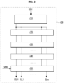
- FIG. 3 is a view illustrating a configuration of a data driver.
- the data driver 400 includes a register unit 410, a first latch 420, a second latch 430, a digital-to-analog converter (DAC) 440, and an output unit 450.
- the register unit 410 samples RGB digital video data bits of the input image using data control signals SSC and SSP provided from the timing controller 200, and provides the sampled digital video data bits to the first latch 420.
- the first latch 420 samples and latches the digital video data bits according to clocks sequentially provided from the register unit 410, and simultaneously outputs the latched data.
- the second latch 430 latches data provided from the first latch 420 and simultaneously outputs latched data in response to a source output enable signal SOE.
- the DAC 440 converts video data input from the second latch unit 430 into a gamma compensation voltage GMA to generate an analog video data voltage.
- the output unit 450 provides an analog type data voltage ADATA output from the DAC 440 to the data lines DL during a low logical period of the source output enable signal SOE.
- the output unit 450 may be implemented as an output buffer outputting a data voltage using a low potential voltage GND and a voltage received through a high potential input terminal, as driving voltages.
- the multiplexer 500 distributes data voltages output from output buffers to the plurality of data lines DL in a time division manner.
- FIG. 1 an embodiment in which 3m number of data lines DL are connected to each output buffer.
- the number of data lines connected to the output buffers is not limited thereto.
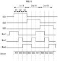
- FIG. 4 is a view illustrating a structure of multiplexers and subpixel arrays according to a first comparative example that represents background art useful for understanding the present disclosure
- FIG. 5 is a view illustrating a timing of control signals and a gate pulse according to the comparative example.
- the display panel 100 includes red subpixels R, green subpixels G, and blue subpixels B disposed in parallel in each pixel line HL.
- the subpixels disposed in each pixel line receive a gate pulse GS1 through the gate line GL.
- subpixels P disposed in a first pixel line HL1 receive a first gate pulse GS1 through a first gate lines GL1.
- subpixels P disposed in a second pixel line HL2 receive a second gate pulse GS2 through a second gate line GL2, and subpixels P disposed in a third pixel line HL3 receive a third gate pulse GS3 through a third gate line GL3.
- Red subpixels R are disposed in a (3m-2)th column line (CL[3m-2]) and green pixels G are disposed in a (3m-1)th column line (CL [3m-1]).
- Blue subpixels B are disposed in a 3mth column line (CL3m).
- red subpixels R are disposed in a first column line CL1 and a fourth column line CL4.
- Green pixels G are disposed in a second column line CL2 and a fifth column line CL5.
- blue subpixels B are disposed in a third column line CL5 and a sixth column line CL6.
- the data driver 400 outputs a data voltage to three subpixels positioned in one pixel line HL during every horizontal period H.
- a first output buffer BUF1 of the data driver 400 sequentially outputs a data voltage applied to R11, G12, and G13 during a first scan period t1 of the first horizontal period 1 st H.
- R (or B or B)xy represents a color and a position of a subpixel. That is, Rab refers to a red subpixel positioned in a horizontal line a and a column line b.
- R11 refers to a red subpixel positioned in a first column line CL1 in the first pixel line HL1. Also, in FIG.
- Data1 illustrates subpixels to which a data voltage output by the first output buffer BUF1 is applied.
- the first horizontal period 1H may be defined as a period during which a data voltage is supplied to the subpixels P disposed in one pixel line HL.
- the data driver 400 supplies the data voltage to three subpixels during the first horizontal period 1H in a time division manner.
- Each of the first to third scan periods t1 to t3 of each horizontal period is defined as a period during which a data voltage applied to one subpixel P is output.
- the multiplexer 500 distributes data voltages, which are output by the output buffers BUF, to a plurality of data lines.
- the multiplexer 500 according to the first comparative example distributes a data voltage output by the first output buffer BUF1 to first to third data lines DL1 to DL3 in a time division manner.
- the multiplexer 500 includes first to third switches M1, M2, and M3.
- the first switch M1 is turned on in response to a first control signal Mux1 to connect the first output buffer BUF1 and the first data line DL1.
- the second switch M2 is turned on in response to a second control signal Mux2 to connect the first output buffer and the second data line DL2, and the third switch M3 is turned on in response to a third control signal Mux3 to connect the first output buffer BUF1 and the third data line DL3.
- the multiplexer controller 600 outputs the first to third control signals in a time division manner during one horizontal period H.
- the multiplexer controller 600 may sequentially output the first, second, and third control signals Mux1, Mux2, and Mux3 or sequentially output the third, second, and first control signals Mux3, Mux2, and Mux1, during one horizontal period.
- the multiplexer controller 600 sequentially outputs the first to third control signals Mux1 to Mux3 during the first horizontal period 1 st H and sequentially outputs the third to first control signals Mux3 to Mux1 during a second horizontal period 2 nd H.
- the first to third control signals Mux1 to Mux3 are sequentially output during each horizontal period H in which the gate pulse GS maintains a gate ON voltage.
- the first gate pulse GS1 maintains the gate ON voltage and the first to third control signals Mux1 to Mux3 are sequentially output.
- the subpixel R11 is charged during the first scan period t1 of the first horizontal period 1 st H
- the subpixel G12 is charged during the second scan period t2 of the first horizontal period 1 st H
- the subpixel B13 is charged during the third scan period t3 of the first horizontal period 1 st H.
- the subpixel R21 is charged during a first scan period t1 of a second horizontal period 2 nd H
- the subpixel G22 is charged during a second scan period t2 of the second horizontal period 2 nd H
- the subpixel B23 is charged during a third scan period t3 of the second horizontal period 2 nd H.
- the third control signal Mux3 is output during the final period of the first horizontal period 1 st H and the first period of the second horizontal period 2 nd H. That is, the number of times the third control signal Mux3 is reversed to a gate ON voltage and the number of times the third control signal Mux3 is reversed to a gate OFF voltage from the first horizontal period 1 st H to the second horizontal period 2 nd H are one time, respectively. Similarly, the number of times the first control signal Mux1 is reversed to a gate ON voltage and the number of times the first control signal Mux1 is reversed to a gate OFF voltage from the second horizontal period 2 nd H to the third horizontal period 3 rd H are one time, respectively.
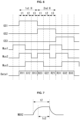
- FIG. 6 is a view illustrating a timing of control signals according to a second comparative example that represents background art useful for understanding the present disclosure.
- a timing for driving the multiplexers and the pixel array illustrated in FIG. 4 is illustrated.
- Detailed descriptions of the same components of the second comparative example illustrated in FIG. 6 as those illustrated in FIG. 5 will be omitted.
- the second control signal Mux2 is output before the second scan period t2 starts, and the third control signal Mux3 is output before the third scan period t3 starts.
- the second control signal Mux2 is output at a timing when the first scan period t1 starts, and the third control signal Mux3 is output at a timing when the second scan period t2 starts.
- the control signals Mux1 to Mux3 output to be adjacent to each other overlap in at least portions thereof.
- the first control signal Mux1 and the second control signal Mux2 partially overlap
- the second control signal Mux2 and the third control signal Mux3 partially overlap.
- control signals Mux1 to Mux3 according to the second comparative example extend in an output period maintained by the gate ON voltage, a sufficient charge period of the data voltage may be secured.
- a period for charging data may be shortened due to delay of the control signals Mux1 to Mux3. For example, as illustrated in FIG. 7 , when the second control signal Mux2 output during the second scan period t2 of the first horizontal period 1 st H is delayed by an RC delay, a period during which data can be charged is "tc2".
- the second control signal Mux2 according to the second comparative example since the second control signal Mux2 according to the second comparative example is output before the second scan period t2, although it is delayed by the RC delay, the second control signal Mux2 may have the gate ON voltage at a timing when the second scan period t2 starts. As a result, the second control signal Mux2 according to the second comparative example may charge the data voltage during the second scan period t2. In this manner, the control signals Mux1 to Mux3 according to the second embedment may sufficiently secure a turn-on period of the switches M1 to M6 to prevent a reduction in a charge time of the data voltage.
- FIG. 8 is a view illustrating a structure of pixel arrays and multiplexers according to an embodiment of the invention as defined in claim 1
- FIG. 9 is a timing diagram of control signals and gate pulses according to the embodiment of the invention as defined in claim 1. Detailed descriptions of the same components of the embodiment illustrated in FIG. 8 as those of the comparative examples described above will be omitted.
- subpixels include a white subpixel W, a red subpixel R, a green subpixel G, and a blue subpixel B.
- W, R, G, and B subpixels are sequentially disposed, and in even-numbered pixel lines HL2 and HL4, G, B, W, and R subpixels are sequentially disposed.
- the W, R, G, and B subpixels disposed in parallel in each pixel line may form a unit pixel.
- W, R, G, and B subpixels disposed in 2x2 unit may form a unit pixel.
- one unit pixel may be used as a reference or two adjacent subpixels may be used as a reference.
- the multiplexer 500 distributes data voltages, which are output by the output buffers BUFs, to a plurality of data lines.
- the multiplexer 500 distributes a positive (+) polarity data voltage, which is output by the first output buffer BUF1, to a first data line DL1, a third data line DL3, a sixth data line DL6, and an eight data line DL8 in a time division manner.
- the multiplexer 500 distributes a negative (-) polarity data voltage, which is output by the second output buffer BUF2, to a second data line DL2, a fourth data line DL4, a fifth data line DL5, and a seventh data line DL7 in a time division manner.
- the multiplexer 500 includes first to eighth switches M1 to M8.
- the first switch M1 is turned on in response to the first control signal Mux1 to connect the first output buffer BUF1 to the first data line DL1.
- the third switch M3 is turned on in response to the third control signal Mux3 to connect the first output buffer BUF1 to the third data line DL3.
- the sixth switch M6 is turned on in response to the second control signal Mux2 to connect the first output buffer BUF1 to the sixth data line DL6.
- the eighth switch M8 is turned in response to the fourth control signal Mux4 to connect the first output buffer BUF1 to the eighth data line DL8.
- the second switch M2 is turned on in response to the second control signal Mux2 to connect the second output buffer BUF2 to the second data line DL2.
- the fourth switch M4 is turned on in response to the fourth control signal Mux4 to connect the second output buffer BUF2 to the fourth data line DL4.
- the fifth switch M5 is turned on in response to the first control signal Mux1 to connect the second output buffer BUF2 to the fifth data line DL5.
- the eighth switch M8 is turned in response to the third control signal Mux3 to connect the second output buffer BUF2 to the seventh data line DL7.
- the multiplexer controller 600 outputs the first to fourth control signals Mux1 to Mux4 in a time division manner during one horizontal period 1H.
- the multiplexer controller 600 sequentially outputs the first control signal Mux1 to the fourth control signal Mux4 or sequentially output the fourth control signal Mux4 to the first control signal Mux1 during one horizontal period.
- the multiplexer controller 600 may sequentially output the first control signal Mux1 to the fourth control signal Mux4 during a first horizontal period 1 st H and sequentially output the fourth control signal Mux4 to the first control signal Mux1 during a second horizontal period 2 nd H.
- first control signal Mux1 to the fourth control signal Mux4 are output during one scan period 1t.
- each of first to fourth scan periods t1 to t4 is defined as a period during which a data voltage applied to one subpixel P is output.
- the data driver 400 outputs data voltages having the opposite polarities through mutually adjacent output buffers.
- the data driver 400 may output a positive (+) polarity data voltage to the output buffer BUF1 and output a negative (-) polarity data voltage to the second output buffer BUF2.
- the data driver 400 outputs a data voltage to one pixel line HL during each horizontal period H.
- Data1 represents subpixels to which a data voltage output by the first output buffer BUF1 is applied
- Data2 represents subpixels to which a data voltage output by the second output buffer BUF2 is applied. That is, the first output buffer BUF1 of the data driver 400 sequentially outputs a data voltage to be supplied to subpixels positioned in a first column line CL1, a third column line CL3, a sixth column line CL6, and an eighth column line CL8 during each horizontal period H.
- the second output buffer BUF2 sequentially outputs a data voltage to be supplied to subpixels positioned in a fifth column line CL5, a second column line CL2, a seventh column line CL7, and a fourth column line CL4 during each horizontal period H.
- a subpixel W11 and a subpixel W15 are charged during a first scan period t1 of the first horizontal period 1 st H.
- a subpixel R16 and a subpixel R12 are charted during a second scan period t2 of the first horizontal period 1 st H.
- a subpixel G13 and a subpixel G17 are charged during a third scan period t3 of the first horizontal period 1 st H.
- a subpixel B18 and a subpixel B14 are charged during a fourth scan period t4 of the first horizontal period 1 st H.
- the control signals Mux are output as a gate ON voltage.
- the data driver 400 outputs a data voltage applied to the subpixel R16 and the subpixel R12.
- the subpixel R16 receives the data voltage through the sixth data line DL6, and the sixth data line DL6 is connected to the first output buffer BUF1 through the sixth switch M6.
- the second control signal Mux2 controlling the sixth switch M6 is output as a gate ON voltage before the second scan period t2.
- the sixth switch M6 may be turned on at a timing when the second scan period t2 starts. As a result, a data charge period may be prevented from being shortened.
Landscapes
- Engineering & Computer Science (AREA)
- Physics & Mathematics (AREA)
- Computer Hardware Design (AREA)
- General Physics & Mathematics (AREA)
- Theoretical Computer Science (AREA)
- Chemical & Material Sciences (AREA)
- Crystallography & Structural Chemistry (AREA)
- Control Of Indicators Other Than Cathode Ray Tubes (AREA)
Description
- The present disclosure relates to a liquid crystal display device which consumes less power.
- A flat panel display device includes a liquid crystal display (LCD), a field emission display (FED), a plasma display panel (PDP), an organic light emitting display device, and the like. In a flat panel display device, data lines and gate lines are disposed to intersect with each other, and regions in which a data line and the gate line intersect with each other is defined as a single subpixel. The subpixel is formed in plurality in a matrix form in a panel. In order to drive each subpixel, a video data voltage desired to be displayed is supplied to the data lines and a gate pulse is sequentially supplied to the gate lines. The video data voltage is supplied to subpixels of a display line to which the gate pulse is supplied, and as all the data lines are sequentially scanned by the gate pulse, video data is displayed.
- A data voltage provided to a data line is generated by a data driver, and the data driver outputs the data voltage through a source channel connected to a data line. Recently, in order to reduce the number of source channels, a structure in which a plurality of data lines are connected to one source channel and a data voltage output to the source channel is supplied to the data lines in a time division manner using a multiplexer may be used. The multiplexer includes switches selectively connecting the source channel and the plurality of data lines, and the switches are turned on in response to a control signal to connect the source channel and one data line.
- As resolution of a display panel is increased, a horizontal period during which a data voltage is supplied to one horizontal line is shortened, and accordingly, an output period of control signals for controlling switches is also shortened. That is, a period during which control signals from the multiplexer are reversed from a gate ON voltage to a gate OFF voltage or from a gate OFF voltage to a gate ON voltage is very short. When reversing of a voltage level of control signals is called transition, control signals transition very frequently for a short period of time, and thus, a circuit section generating a control signal consumes a large amount of power.
- Also, as resolution is lowered, a period during which control signals controlling the multiplexer maintain the gate ON voltage is so short that a data charge rate is shortened.
-
US 2013/141320 A1 discloses that a liquid crystal display generates k DEMUX control signals for controlling the turn-on time of the DEMUX switches so as not to overlap with each other, and generates at least some of the DEMUX control signals every 2 horizontal periods, and makes 1 pulse sustaining period of the DEMUX control signals generated every 2 horizontal periods to overlap with a tail portion of the preceding horizontal period and a front portion of the subsequent horizontal period, among two neighboring horizontal periods. -
US 2007/091050 A1 discloses that in a display device using an RGB time division drive system in which RGB data to be supplied to display pixels of three colors RGB are subjected to time-division multiplexing and input to a liquid crystal panel unit, data are input to the liquid crystal panel unit alternately in the order of RGB and BGR every line signal, and a selection signal SC which is in the on-state at a break of one line period is kept in the on-state until the next line period. In addition, over a partial non-display period in partial display, selection signals SA, SB and SC are always in the off-state and an equalize signal EQG is in the on-state. -
US 2016/078826 A1 discloses that a display device includes a pixel array having a plurality of pixels arranged in a matrix form based on a crossing structure of data lines and gate lines, a data driver having a plurality of output channels and configured to output a data voltage, a multiplexer configured to distribute the data voltage output from the data driver to the data lines in response to first and second control signals, and a gate driver configured to output a gate pulse synchronized with the data voltage in a non-sequential manner. The first and second control signals are in antiphase, and a switching cycle of the first and second control signals is one horizontal period or two horizontal periods. -
US 2016/078836 A1 discloses that a display device includes pixels arranged in a matrix form, gate lines extending in a first direction; data lines extending in a second direction, first and second unit pixel columns, each defined by adjacent data lines and the pixels connected thereto, first and second channels which transmit data signals to each of the first and second unit pixel columns, and a line selector which connects the first and second channels to the data lines and provides data voltages to the data lines in response to control signals, where a pixel connected to a first gate line is connected to a data line at a side thereof, a pixel connected to a second gate line is connected to a data line at the other side thereof, and each of the first and second channels is connected to a data line of each of the first and second unit pixel columns. -
US 2004/179014 A1 discloses that a liquid crystal panel is provided with a connection switching circuit for connecting a video signal line driving circuit to a plurality of video signal lines. The connection switching circuit includes analog switches that correspond to the video signal lines and one side of each of the analog switches is connected to one of the video signal lines. The video signal lines are grouped together into groups of two video signal lines that are spaced apart by one video signal line. The groups of video signal lines respectively correspond to output terminals of the video signal line driving circuit. The other sides of the analog switches connected to the video signal lines of the same group are connected to one another, and connected to one output terminal. Based on a switching control signal, the analog switches connect each of the output terminals in each horizontal scanning period by time division to the two video signal lines of the corresponding group. -
US 2016/322008 A1 discloses a display device. A display panel includes a plurality of subpixels of a plurality of colors arranged in a matrix form, and a plurality of gate lines and data lines respectively connected to the subpixels. A data driver is configured to supply data voltages to the subpixels through a plurality of source channels and the data lines. A switch circuit is configured to connect one of the source channels selectively to one of the data lines during a first scan period in one horizontal period and to a different one of the data lines during a second scan period in the one horizontal period. The data driver is configured to supply data voltages of one color to the one of the source channels during both the first scan period and the second scan period in the one horizontal period. -
US 2016/189657 A1 discloses that a display device includes a display panel including a plurality of data lines, a data driver to supply a source voltage to each data line through a source line, a switching circuit to connect each data line to the source line, and a multiplexer controller to produce a control signal operating the switching circuit and vary a voltage level of the control signal depending on the source voltage. -
CN 105 590 600 A discloses a display, which comprises a first switch unit used for receiving a first turn-on signal and conducting a first polarity data signal to a first sub-pixel; a second switch unit used for receiving a second turn-on signal and conducting the first polarity data signal to a sixth sub-pixel; a third switch unit used for receiving a third turn-on signal and conducting the first polarity data signal to a seventh sub-pixel; a fourth switch unit used for receiving a fourth turn-on signal and conducting the first polarity data signal to a fourth sub-pixel; a fifth switch unit used for receiving the first turn-on signal and conducting a second polarity data signal to a fifth sub-pixel; a sixth switch unit used for receiving the second turn-on signal and conducting the second polarity data signal to a second sub-pixel; a seventh switch unit used for receiving a third turn-on signal and conducting the second polarity data signal to a third sub-pixel; and an eighth switch unit used for receiving a fourth turn-on signal and conducting the second polarity data signal to an eighth sub-pixel. -
CN 105 185 326 A describes a liquid crystal display panel and a driving circuit thereof. The liquid crystal display panel comprises multiple source driving circuits and multiple sub pixel rows arranged along the column direction. Each sub pixel row comprises multiple sub pixels of different colors arranged cyclically along the row direction. In the same scanning frame, the driving voltages of at least one sub pixel in each arrangement cycle are opposite in polarity. Each source driving circuit is provided with at least two output ports, and the at least two output ports are respectively connected to at least two sub pixels of which the driving voltages are of the same polarity in the same scanning frame in order to provide driving voltages of the same polarity. -
CN 106 057 164 A describes an RGBW four primary color panel driving framework. The RGBW four primary color panel driving framework is characterized in that subpixels on the RGBW four primary color panel are arranged in an array mode; the twelve subpixels which are connected to one scanning line n and are continuously arranged are formed through arranging a red subpixel R, a green subpixel G, a blue subpixel B and a white subpixel W according to a specific sequence, repeating the specific sequence and arranging the subpixels for three times; two adjacent data lines n and a data line n+1 are connected respectively so as to drive the subpixels on an odd number sequence and an even number sequence in the twelve subpixels; and signal polarities on the data lines n and the data line n+1 are opposite. - According to an aspect of the present disclosure, a display device includes a data driver, a multiplexer, and a multiplexer controller. The data driver outputs a data voltage through an output buffer. The multiplexer distributes data voltages, which are respectively output by output buffers, to n number of data lines in a time division manner, in response to first to nth (n is a natural number of 2 or greater) control signals. The multiplexer controller outputs first to nth control signals in a time division manner during one horizontal period. An ith (i is a natural number of n or smaller) control signal maintaining a gate ON voltage at a timing when a first horizontal period expires maintains the gate ON voltage for a predetermined period of time after a second horizontal period starts.
- The present disclosure provides a display device according to
claim 1. Further embodiments are described in the dependent claim. - The above and other aspects, features, and advantages of the present disclosure will be more clearly understood from the following detailed description taken in conjunction with the accompanying drawings, in which:
-
FIG. 1 is a view illustrating a display device according to an embodiment of the present disclosure. -
FIG. 2 is a view illustrating an example of a subpixel illustrated inFIG. 1 . -
FIG. 3 is a view illustrating an example of a data driver. -
FIG. 4 is a view illustrating a structure of multiplexers and subpixel arrays according to a first comparative example that represents background art useful for understanding the present disclosure. -
FIG. 5 is a view illustrating a timing of control signals according to the first comparative example that represents background art useful for understanding the present disclosure. -
FIG. 6 is a view illustrating a timing of control signals according to a second comparative example that represents background art useful for understanding the present disclosure. -
FIG. 7 is a view illustrating a data charge time reduced due to a multiplexer control signal delay phenomenon. -
FIG. 8 is a view illustrating a structure of multiplexers and subpixel arrays according to an embodiment of the invention as defined inclaim 1. -
FIG. 9 is a timing diagram of control signals according to the embodiment of the invention as defined inclaim 1. - Hereinafter, embodiments of the present disclosure will be described in detail with reference to the accompanying drawings. Like reference numerals refer to like elements throughout. In describing the present invention, if a detailed explanation for a related known function or construction is considered to unnecessarily divert the gist of the present invention, such explanation will be omitted but would be understood by those skilled in the art.
- In a gate driver of the present disclosure, switches may be implemented as transistors having a structure of n-type or p-type metal oxide semiconductor field effect transistors (MOSFETs). In the embodiments described hereinafter, an n-type transistor will be described, but the present disclosure is not limited thereto. In the present disclosure, outputting control signals refers to a state in which the corresponding control signals are in a gate ON voltage state. That is, gate ON voltage of the switches as n type transistors correspond to a high potential voltage and outputting or applying control signals refers to a state in which corresponding control signals are in a high potential voltage state.
-
FIG. 1 is a view illustrating a display device according to an embodiment of the present disclosure, andFIG. 2 is a view illustrating an example of a subpixel illustrated inFIG. 1 . - Referring to
FIGS. 1 and 2 , the display device of the present disclosure includes adisplay panel 100, atiming controller 200, agate driver 300, adata driver 400, amultiplexer 500, and amultiplexer controller 600. - The
display panel 100, including a subpixel array in which subpixels are disposed in a matrix form, displays input image data. As illustrated inFIG. 2 , the subpixel array includes a thin film transistor (TFT) array formed on a lower substrate, a color filter array formed on an upper substrate, and liquid crystal cells Clc. The TFT array includes a data line DL and a gate line GL intersecting with the data line DL, a TFT formed at a crossing between the data line DL and the gate line GL, asubpixel electrode 1 connected to the TFT, a storage capacitor Cst, and the like. The color filter array includes a black matrix and a color filter. Acommon electrode 2 may be formed on the lower substrate or upper substrate. Liquid crystal cells Clc are driven by an electric field between thesubpixel electrode 1 to which a data voltage is supplied and thecommon electrode 2 to which a common voltage Vcom is supplied. - The
timing controller 200 may receive digital video data RGB from an external host and receives timing signals such as a vertical synchronization signal Vsync, a horizontal synchronization signal Hsync, a data enable signal DE, a main clock CLK, and the like. Thetiming controller 200 transmits the digital video signal RGB to thedata driver 400. Thetiming controller 200 generates a source timing control signal for controlling an operation timing of thedata driver 400 using the timing signals Vsync, Hsync, DE, and CLK and gate timing control signals ST, GCLK, and MCLK for controlling an operation timing of a level shifter and a shift register of thegate driver 300. - The
gate driver 300 outputs a gate pulse Gout using a gate timing control signal. The gate timing control signal includes a gate start pulse (GSP), a gate shift clock (GSC), and a gate output enable (GOE). The gate start pulse (GSP) indicates a starting line for thegate driver 300 to output a first gate pulse Gout. The gate shift clock (GSC) is a clock for shifting the gate start pulse (GSP). The gate output enable (GOE) sets an output period of the gate pulse Gout. Thegate driver 300 may be implemented in the form of a gate-in-panel (GIP) including a combination of TFTs on thedisplay panel 100. - The
data driver 400 converts image data provided from thetiming controller 200 into a data voltage. -
FIG. 3 is a view illustrating a configuration of a data driver. - Referring to
FIG. 3 , thedata driver 400 includes aregister unit 410, afirst latch 420, asecond latch 430, a digital-to-analog converter (DAC) 440, and anoutput unit 450. Theregister unit 410 samples RGB digital video data bits of the input image using data control signals SSC and SSP provided from thetiming controller 200, and provides the sampled digital video data bits to thefirst latch 420. Thefirst latch 420 samples and latches the digital video data bits according to clocks sequentially provided from theregister unit 410, and simultaneously outputs the latched data. Thesecond latch 430 latches data provided from thefirst latch 420 and simultaneously outputs latched data in response to a source output enable signal SOE. TheDAC 440 converts video data input from thesecond latch unit 430 into a gamma compensation voltage GMA to generate an analog video data voltage. Theoutput unit 450 provides an analog type data voltage ADATA output from theDAC 440 to the data lines DL during a low logical period of the source output enable signal SOE. Theoutput unit 450 may be implemented as an output buffer outputting a data voltage using a low potential voltage GND and a voltage received through a high potential input terminal, as driving voltages. - The
multiplexer 500 distributes data voltages output from output buffers to the plurality of data lines DL in a time division manner. InFIG. 1 , an embodiment in which 3m number of data lines DL are connected to each output buffer. However, the number of data lines connected to the output buffers is not limited thereto. -
FIG. 4 is a view illustrating a structure of multiplexers and subpixel arrays according to a first comparative example that represents background art useful for understanding the present disclosure, andFIG. 5 is a view illustrating a timing of control signals and a gate pulse according to the comparative example. - Referring to
FIGS. 4 and5 , thedisplay panel 100 includes red subpixels R, green subpixels G, and blue subpixels B disposed in parallel in each pixel line HL. The subpixels disposed in each pixel line receive a gate pulse GS1 through the gate line GL. For example, subpixels P disposed in a first pixel line HL1 receive a first gate pulse GS1 through a first gate lines GL1. Also, subpixels P disposed in a second pixel line HL2 receive a second gate pulse GS2 through a second gate line GL2, and subpixels P disposed in a third pixel line HL3 receive a third gate pulse GS3 through a third gate line GL3. Red subpixels R are disposed in a (3m-2)th column line (CL[3m-2]) and green pixels G are disposed in a (3m-1)th column line (CL [3m-1]). Blue subpixels B are disposed in a 3mth column line (CL3m). For example, red subpixels R are disposed in a first column line CL1 and a fourth column line CL4. Green pixels G are disposed in a second column line CL2 and a fifth column line CL5. Also, blue subpixels B are disposed in a third column line CL5 and a sixth column line CL6. - The
data driver 400 outputs a data voltage to three subpixels positioned in one pixel line HL during every horizontal period H. For example, a first output buffer BUF1 of thedata driver 400 sequentially outputs a data voltage applied to R11, G12, and G13 during a first scan period t1 of the firsthorizontal period 1st H. In this comparative example, R (or B or B)xy represents a color and a position of a subpixel. That is, Rab refers to a red subpixel positioned in a horizontal line a and a column line b. Thus, R11 refers to a red subpixel positioned in a first column line CL1 in the first pixel line HL1. Also, inFIG. 5 , Data1 illustrates subpixels to which a data voltage output by the first output buffer BUF1 is applied. Also, the first horizontal period 1H may be defined as a period during which a data voltage is supplied to the subpixels P disposed in one pixel line HL. Thedata driver 400 supplies the data voltage to three subpixels during the first horizontal period 1H in a time division manner. Each of the first to third scan periods t1 to t3 of each horizontal period is defined as a period during which a data voltage applied to one subpixel P is output. - The
multiplexer 500 distributes data voltages, which are output by the output buffers BUF, to a plurality of data lines. Themultiplexer 500 according to the first comparative example distributes a data voltage output by the first output buffer BUF1 to first to third data lines DL1 to DL3 in a time division manner. To this end, themultiplexer 500 includes first to third switches M1, M2, and M3. The first switch M1 is turned on in response to a first control signal Mux1 to connect the first output buffer BUF1 and the first data line DL1. The second switch M2 is turned on in response to a second control signal Mux2 to connect the first output buffer and the second data line DL2, and the third switch M3 is turned on in response to a third control signal Mux3 to connect the first output buffer BUF1 and the third data line DL3. - The
multiplexer controller 600 outputs the first to third control signals in a time division manner during one horizontal period H. Themultiplexer controller 600 may sequentially output the first, second, and third control signals Mux1, Mux2, and Mux3 or sequentially output the third, second, and first control signals Mux3, Mux2, and Mux1, during one horizontal period. For example, themultiplexer controller 600 sequentially outputs the first to third control signals Mux1 to Mux3 during the first horizontal period 1st H and sequentially outputs the third to first control signals Mux3 to Mux1 during a second horizontal period 2nd H. - The first to third control signals Mux1 to Mux3 are sequentially output during each horizontal period H in which the gate pulse GS maintains a gate ON voltage. For example, during the first horizontal period 1H, the first gate pulse GS1 maintains the gate ON voltage and the first to third control signals Mux1 to Mux3 are sequentially output.
- As a result, the subpixel R11 is charged during the first scan period t1 of the first horizontal period 1st H, the subpixel G12 is charged during the second scan period t2 of the first horizontal period 1st H, and the subpixel B13 is charged during the third scan period t3 of the first horizontal period 1st H.
- Also, the subpixel R21 is charged during a first scan period t1 of a second horizontal period 2nd H, the subpixel G22 is charged during a second scan period t2 of the second horizontal period 2nd H, and the subpixel B23 is charged during a third scan period t3 of the second horizontal period 2nd H.
- In this manner, in the first comparative example, the third control signal Mux3 is output during the final period of the first horizontal period 1st H and the first period of the second
horizontal period 2nd H. That is, the number of times the third control signal Mux3 is reversed to a gate ON voltage and the number of times the third control signal Mux3 is reversed to a gate OFF voltage from the first horizontal period 1st H to the second horizontal period 2nd H are one time, respectively. Similarly, the number of times the first control signal Mux1 is reversed to a gate ON voltage and the number of times the first control signal Mux1 is reversed to a gate OFF voltage from the second horizontal period 2nd H to the third horizontal period 3rd H are one time, respectively. - As a result, overall transition number of the control signals Mux1 to Mux3 output by the
multiplexer controller 600 is reduced, and thus, power consumption of themultiplexer controller 600 is reduced. -
FIG. 6 is a view illustrating a timing of control signals according to a second comparative example that represents background art useful for understanding the present disclosure. InFIG. 6 , a timing for driving the multiplexers and the pixel array illustrated inFIG. 4 is illustrated. Detailed descriptions of the same components of the second comparative example illustrated inFIG. 6 as those illustrated inFIG. 5 will be omitted. - Referring to
FIG. 6 , the second control signal Mux2 is output before the second scan period t2 starts, and the third control signal Mux3 is output before the third scan period t3 starts. For example, the second control signal Mux2 is output at a timing when the first scan period t1 starts, and the third control signal Mux3 is output at a timing when the second scan period t2 starts. As a result, the control signals Mux1 to Mux3 output to be adjacent to each other overlap in at least portions thereof. For example, the first control signal Mux1 and the second control signal Mux2 partially overlap, and the second control signal Mux2 and the third control signal Mux3 partially overlap. - In this manner, since the control signals Mux1 to Mux3 according to the second comparative example extend in an output period maintained by the gate ON voltage, a sufficient charge period of the data voltage may be secured.
- In the first comparative example, a period for charging data may be shortened due to delay of the control signals Mux1 to Mux3. For example, as illustrated in
FIG. 7 , when the second control signal Mux2 output during the second scan period t2 of the first horizontal period 1st H is delayed by an RC delay, a period during which data can be charged is "tc2". - In contrast, since the second control signal Mux2 according to the second comparative example is output before the second scan period t2, although it is delayed by the RC delay, the second control signal Mux2 may have the gate ON voltage at a timing when the second scan period t2 starts. As a result, the second control signal Mux2 according to the second comparative example may charge the data voltage during the second scan period t2. In this manner, the control signals Mux1 to Mux3 according to the second embedment may sufficiently secure a turn-on period of the switches M1 to M6 to prevent a reduction in a charge time of the data voltage.
-
FIG. 8 is a view illustrating a structure of pixel arrays and multiplexers according to an embodiment of the invention as defined inclaim 1, andFIG. 9 is a timing diagram of control signals and gate pulses according to the embodiment of the invention as defined inclaim 1. Detailed descriptions of the same components of the embodiment illustrated inFIG. 8 as those of the comparative examples described above will be omitted. - Referring to
FIGS. 8 and9 , subpixels include a white subpixel W, a red subpixel R, a green subpixel G, and a blue subpixel B. - In odd-numbered pixel lines HL1 and HL3, W, R, G, and B subpixels are sequentially disposed, and in even-numbered pixel lines HL2 and HL4, G, B, W, and R subpixels are sequentially disposed. Thus, the W, R, G, and B subpixels disposed in parallel in each pixel line may form a unit pixel. Alternately, W, R, G, and B subpixels disposed in 2x2 unit may form a unit pixel. In image rendering of the display panel, one unit pixel may be used as a reference or two adjacent subpixels may be used as a reference.
- The
multiplexer 500 distributes data voltages, which are output by the output buffers BUFs, to a plurality of data lines. Themultiplexer 500 distributes a positive (+) polarity data voltage, which is output by the first output buffer BUF1, to a first data line DL1, a third data line DL3, a sixth data line DL6, and an eight data line DL8 in a time division manner. Also, themultiplexer 500 distributes a negative (-) polarity data voltage, which is output by the second output buffer BUF2, to a second data line DL2, a fourth data line DL4, a fifth data line DL5, and a seventh data line DL7 in a time division manner. - To this end, the
multiplexer 500 includes first to eighth switches M1 to M8. - The first switch M1 is turned on in response to the first control signal Mux1 to connect the first output buffer BUF1 to the first data line DL1. The third switch M3 is turned on in response to the third control signal Mux3 to connect the first output buffer BUF1 to the third data line DL3. The sixth switch M6 is turned on in response to the second control signal Mux2 to connect the first output buffer BUF1 to the sixth data line DL6. The eighth switch M8 is turned in response to the fourth control signal Mux4 to connect the first output buffer BUF1 to the eighth data line DL8.
- The second switch M2 is turned on in response to the second control signal Mux2 to connect the second output buffer BUF2 to the second data line DL2. The fourth switch M4 is turned on in response to the fourth control signal Mux4 to connect the second output buffer BUF2 to the fourth data line DL4. The fifth switch M5 is turned on in response to the first control signal Mux1 to connect the second output buffer BUF2 to the fifth data line DL5. The eighth switch M8 is turned in response to the third control signal Mux3 to connect the second output buffer BUF2 to the seventh data line DL7.
- The
multiplexer controller 600 outputs the first to fourth control signals Mux1 to Mux4 in a time division manner during one horizontal period 1H. Themultiplexer controller 600 sequentially outputs the first control signal Mux1 to the fourth control signal Mux4 or sequentially output the fourth control signal Mux4 to the first control signal Mux1 during one horizontal period. For example, themultiplexer controller 600 may sequentially output the first control signal Mux1 to the fourth control signal Mux4 during a first horizontal period 1st H and sequentially output the fourth control signal Mux4 to the first control signal Mux1 during a second horizontal period 2nd H. - Within one horizontal period 1H, the first control signal Mux1 to the fourth control signal Mux4 are output during one scan period 1t. Within each horizontal period H, each of first to fourth scan periods t1 to t4 is defined as a period during which a data voltage applied to one subpixel P is output.
- The
data driver 400 outputs data voltages having the opposite polarities through mutually adjacent output buffers. For example, thedata driver 400 may output a positive (+) polarity data voltage to the output buffer BUF1 and output a negative (-) polarity data voltage to the second output buffer BUF2. - The
data driver 400 outputs a data voltage to one pixel line HL during each horizontal period H. InFIG. 9 , Data1 represents subpixels to which a data voltage output by the first output buffer BUF1 is applied, and Data2 represents subpixels to which a data voltage output by the second output buffer BUF2 is applied. That is, the first output buffer BUF1 of thedata driver 400 sequentially outputs a data voltage to be supplied to subpixels positioned in a first column line CL1, a third column line CL3, a sixth column line CL6, and an eighth column line CL8 during each horizontal period H. The second output buffer BUF2 sequentially outputs a data voltage to be supplied to subpixels positioned in a fifth column line CL5, a second column line CL2, a seventh column line CL7, and a fourth column line CL4 during each horizontal period H. - As a result, a subpixel W11 and a subpixel W15 are charged during a first scan period t1 of the first
horizontal period 1st H. A subpixel R16 and a subpixel R12 are charted during a second scan period t2 of the firsthorizontal period 1st H. A subpixel G13 and a subpixel G17 are charged during a third scan period t3 of the firsthorizontal period 1st H. A subpixel B18 and a subpixel B14 are charged during a fourth scan period t4 of the first horizontal period 1st H. - Also, before a data voltage is applied to the data line DL, the control signals Mux are output as a gate ON voltage. For example, during the second scan period t2, the
data driver 400 outputs a data voltage applied to the subpixel R16 and the subpixel R12. The subpixel R16 receives the data voltage through the sixth data line DL6, and the sixth data line DL6 is connected to the first output buffer BUF1 through the sixth switch M6. The second control signal Mux2 controlling the sixth switch M6 is output as a gate ON voltage before the second scan period t2. Thus, although the second control signal Mux2 is delayed, the sixth switch M6 may be turned on at a timing when the second scan period t2 starts. As a result, a data charge period may be prevented from being shortened. - Although embodiments have been described with reference to a number of illustrative embodiments thereof, it should be understood that numerous other modifications and embodiments can be devised by those skilled in the art that will fall within the scope of the claims. More particularly, various variations and modifications are possible in the component parts and/or arrangements of the subject combination arrangement within the scope of the appended claims.
Claims (2)
- A liquid crystal display device comprising:a display panel (100) comprising a plurality of four color subpixels sequentially disposed in a pixel line;a plurality of data lines, wherein a first data line (DL1) is connected to a first color subpixel of a first pixel, a second data line (DL2) is connected to a second color subpixel of the first pixel, a third data line (DL3) is connected to a third color subpixel of the first pixel, a fourth data line (DL4) is connected to a fourth color subpixel of the first pixel, a fifth data line (DL5) is connected to a first color subpixel of a second pixel, a sixth data line (DL6) is connected to a second color subpixel of the second pixel, a seventh data line (DL7) is connected to a third color subpixel of the second pixel, and an eighth data line (DL8) is connected to a fourth color subpixel of the second pixel,a data driver (400);the data driver (400) including a first output buffer (BUF1) configured to output a positive polarity data voltage and a second output buffer (BUF2) configured to output a negative polarity data voltage;the data driver (400) configured to output data voltages through the first and second output buffers (BUF1, BUF2);a multiplexer (500) configured to distribute the data voltages, which are respectively output by the first and second output buffers (BUF1, BUF2), to the first to eighth data lines (DL1, ... , DL8), in response to first to fourth control signals (Mux1, Mux2, Mux3, Mux4); anda multiplexer controller (600) configured to output the first to fourth control signals (Mux1, Mux2, Mux3, Mux4) in a time division manner during one horizontal period, wherein the fourth control signal (Mux4) maintaining a gate ON voltage at a timing when a first horizontal period (1st H) expires maintains the gate ON voltage for a predetermined period of time after a second horizontal period starts,the multiplexer (500) includes a first switch (M1), a third switch (M3), a sixth switch (M6), and an eighth switch (M8) configured to distribute a data voltage from the first output buffer (BUF1) to the first data line (DL1), the third data line (DL3), the sixth data line (DL6), and the eighth data line (DL8) in a time division manner and a second switch (M2), a fourth switch (M4), a fifth switch (M5), and a seventh switch (M7) configured to distribute a data voltage from the second output buffer (BUF2) to the second data line (DL2), the fourth data line (DL4), the fifth data line (DL5), and the seventh data line (DL7) in a time division manner, andthe multiplexer controller (600) is configured to outputthe first control signal (Mux1) controlling the first and fifth switch (M1, M5);the second control signal (Mux2) controlling the second and sixth switch (M2, M6);the third control signal (Mux3) controlling the third and seventh switch (M3, M7); andthe fourth control signal (Mux4) controlling the fourth and eighth switch (M4, M8),wherein:each of the first horizontal period (1st H) and the second horizontal period includes first to fourth scan periods (t1, t2, t3, t4),the data driver (400) is configured to output a data voltage to be supplied to one subpixel during one scan period,the multiplexer controller (600) is configured to sequentially output the first control signal (Mux1) to the fourth control signal (Mux4) during the first horizontal period (1st H), and sequentially output the fourth control signal (Mux4) to the first control signal (Mux1) during the second horizontal period in the reverse order to the first horizontal period (1st H),and wherein in the first horizontal period (1st H):the second control signal (Mux2) starts to be output as a gate ON voltage during the first scan period (t1) so that a portion of the second control signal (Mux2) overlaps a portion of the first control signal (Mux1),the third control signal (Mux3) starts to be output as a gate ON voltage during the second scan period (t2) so that a portion of the third control signal (Mux3) overlaps a portion of the second control signal (Mux2), andthe fourth control signal (Mux4) starts to be output as a gate ON voltage during the third scan period (t3) so that a portion of the fourth control signal (Mux4) overlaps a portion of the third control signal (Mux3).
- The display device of claim 1, wherein
in the second horizontal period:the third control signal (Mux3) starts to be output as a gate ON voltage during the first scan period (t1) so that a portion of the third control signal (Mux3) overlaps a portion of the fourth control signal (Mux4),the second control signal (Mux2) starts to be output as a gate ON voltage during the second scan period (t2) so that a portion of the second control signal (Mux2) overlaps a portion of the third control signal (Mux3), andthe first control signal (Mux1) starts to be output as a gate ON voltage during the third scan period (t3) so that a portion of the first control signal (Mux2) overlaps a portion of the second control signal (Mux2).
Applications Claiming Priority (1)
| Application Number | Priority Date | Filing Date | Title |
|---|---|---|---|
| KR1020160158735A KR20180059664A (en) | 2016-11-25 | 2016-11-25 | Display Device |
Publications (2)
| Publication Number | Publication Date |
|---|---|
| EP3327715A1 EP3327715A1 (en) | 2018-05-30 |
| EP3327715B1 true EP3327715B1 (en) | 2023-10-04 |
Family
ID=60331497
Family Applications (1)
| Application Number | Title | Priority Date | Filing Date |
|---|---|---|---|
| EP17202048.9A Active EP3327715B1 (en) | 2016-11-25 | 2017-11-16 | Display device |
Country Status (4)
| Country | Link |
|---|---|
| US (1) | US10593278B2 (en) |
| EP (1) | EP3327715B1 (en) |
| KR (1) | KR20180059664A (en) |
| CN (1) | CN108109572B (en) |
Families Citing this family (15)
| Publication number | Priority date | Publication date | Assignee | Title |
|---|---|---|---|---|
| US20200135110A1 (en) * | 2017-03-24 | 2020-04-30 | Sharp Kabushiki Kaisha | Display device and driving method therefor |
| US10748466B2 (en) * | 2018-09-20 | 2020-08-18 | Wuhan China Star Optoelectronics Semiconductor Display Technology Co., Ltd. | Display panel and method of driving the same |
| KR102717206B1 (en) * | 2019-03-05 | 2024-10-14 | 삼성디스플레이 주식회사 | Data driving apparatus and display apparatus including the same |
| JP7367006B2 (en) * | 2019-04-12 | 2023-10-23 | ラピスセミコンダクタ株式会社 | Display driver and display device |
| KR102717975B1 (en) * | 2019-05-14 | 2024-10-17 | 삼성디스플레이 주식회사 | Display device and method of driving the same |
| KR102623781B1 (en) * | 2019-09-10 | 2024-01-10 | 엘지디스플레이 주식회사 | Display apparatus |
| CN110658659B (en) * | 2019-10-12 | 2021-03-23 | Tcl华星光电技术有限公司 | Liquid crystal display circuit, liquid crystal display circuit driving method and display panel |
| KR102716379B1 (en) * | 2019-12-20 | 2024-10-14 | 엘지디스플레이 주식회사 | Display device |
| TWI729907B (en) * | 2020-08-14 | 2021-06-01 | 凌巨科技股份有限公司 | Display and multiplexer for display |
| KR102765887B1 (en) | 2020-12-29 | 2025-02-07 | 엘지디스플레이 주식회사 | Display Device Including Multiplexer And Method Of Driving The Same |
| CN115315742B (en) * | 2021-03-04 | 2025-04-11 | 京东方科技集团股份有限公司 | Light-emitting substrate, display device, and method for driving the light-emitting substrate |
| TWI796138B (en) * | 2021-03-08 | 2023-03-11 | 瑞鼎科技股份有限公司 | Display driving device and method with low power consumption |
| EP4385005A1 (en) | 2022-10-31 | 2024-06-19 | Google LLC | Display device with variable image resolution |
| KR20250100162A (en) * | 2023-12-26 | 2025-07-03 | 엘지디스플레이 주식회사 | Data driver and display device including the same |
| TWI872883B (en) | 2023-12-27 | 2025-02-11 | 友達光電股份有限公司 | Display driving device |
Citations (2)
| Publication number | Priority date | Publication date | Assignee | Title |
|---|---|---|---|---|
| CN105185326A (en) * | 2015-08-12 | 2015-12-23 | 深圳市华星光电技术有限公司 | Liquid crystal display panel and driving circuit thereof |
| CN106057164A (en) * | 2016-08-10 | 2016-10-26 | 武汉华星光电技术有限公司 | RGBW four primary color panel driving framework |
Family Cites Families (19)
| Publication number | Priority date | Publication date | Assignee | Title |
|---|---|---|---|---|
| KR100367010B1 (en) * | 2000-06-08 | 2003-01-09 | 엘지.필립스 엘시디 주식회사 | Liquid Crystal Display and Method of Driving the same |
| JP2004264476A (en) * | 2003-02-28 | 2004-09-24 | Sharp Corp | Display device and driving method thereof |
| JP4786996B2 (en) * | 2005-10-20 | 2011-10-05 | 株式会社 日立ディスプレイズ | Display device |
| JP2009168849A (en) | 2008-01-10 | 2009-07-30 | Seiko Epson Corp | Electro-optical device, driving method of electro-optical device, and electronic apparatus |
| KR101985247B1 (en) * | 2011-12-02 | 2019-06-04 | 엘지디스플레이 주식회사 | LCD and driving method thereof |
| KR102034236B1 (en) * | 2013-01-17 | 2019-10-21 | 삼성디스플레이 주식회사 | Organic Light Emitting Display Device |
| KR102058856B1 (en) * | 2013-12-31 | 2019-12-24 | 엘지디스플레이 주식회사 | Liquid crystal display device |
| CN104090440B (en) | 2014-06-30 | 2017-01-18 | 上海天马微电子有限公司 | Pixel structure, liquid crystal display array substrate and liquid crystal display panel |
| KR102233626B1 (en) * | 2014-09-15 | 2021-04-01 | 삼성디스플레이 주식회사 | Display device |
| KR102219667B1 (en) * | 2014-09-17 | 2021-02-24 | 엘지디스플레이 주식회사 | Display device |
| JP2016062076A (en) * | 2014-09-22 | 2016-04-25 | Nltテクノロジー株式会社 | Pixel circuit, method for driving the same and display device |
| US20160093260A1 (en) * | 2014-09-29 | 2016-03-31 | Innolux Corporation | Display device and associated method |
| US20170358268A1 (en) * | 2014-11-28 | 2017-12-14 | Sharp Kabushiki Kaisha | Data signal line drive circuit, display device provided with same, and method for driving same |
| KR102298849B1 (en) * | 2014-12-31 | 2021-09-09 | 엘지디스플레이 주식회사 | Display Device |
| KR102350392B1 (en) * | 2015-04-30 | 2022-01-17 | 엘지디스플레이 주식회사 | Display Device |
| CN105047162B (en) * | 2015-08-26 | 2018-09-11 | 深圳市华星光电技术有限公司 | Array substrate and its driving method |
| CN105590600A (en) * | 2015-12-15 | 2016-05-18 | 武汉华星光电技术有限公司 | Display and driving method thereof |
| KR102423443B1 (en) | 2016-01-15 | 2022-07-21 | 삼성디스플레이 주식회사 | Liquid crystal display device and manufacturing method thereof |
| KR20170088011A (en) | 2016-01-21 | 2017-08-01 | 삼성디스플레이 주식회사 | Display apparatus |
-
2016
- 2016-11-25 KR KR1020160158735A patent/KR20180059664A/en not_active Ceased
-
2017
- 2017-11-16 EP EP17202048.9A patent/EP3327715B1/en active Active
- 2017-11-27 US US15/822,906 patent/US10593278B2/en active Active
- 2017-11-27 CN CN201711204196.6A patent/CN108109572B/en active Active
Patent Citations (4)
| Publication number | Priority date | Publication date | Assignee | Title |
|---|---|---|---|---|
| CN105185326A (en) * | 2015-08-12 | 2015-12-23 | 深圳市华星光电技术有限公司 | Liquid crystal display panel and driving circuit thereof |
| US20170221436A1 (en) * | 2015-08-12 | 2017-08-03 | Shenzhen China Star Optoelectronics Technology Co., Ltd. | Liquid crystal panels and the driving circuits thereof |
| CN106057164A (en) * | 2016-08-10 | 2016-10-26 | 武汉华星光电技术有限公司 | RGBW four primary color panel driving framework |
| US10008163B1 (en) * | 2016-08-10 | 2018-06-26 | Wuhan China Star Optoelectronics Technology Co., Ltd. | Driver structure for RGBW four-color panel |
Also Published As
| Publication number | Publication date |
|---|---|
| CN108109572B (en) | 2021-06-15 |
| CN108109572A (en) | 2018-06-01 |
| EP3327715A1 (en) | 2018-05-30 |
| KR20180059664A (en) | 2018-06-05 |
| US20180151137A1 (en) | 2018-05-31 |
| US10593278B2 (en) | 2020-03-17 |
Similar Documents
| Publication | Publication Date | Title |
|---|---|---|
| EP3327716B1 (en) | Display device | |
| EP3089150B1 (en) | Display device | |
| CN108109572B (en) | Display device | |
| US8587504B2 (en) | Liquid crystal display and method of driving the same | |
| US8154498B2 (en) | Display device | |
| KR101385225B1 (en) | Liquid crystal display and method for driving the same | |
| US8963912B2 (en) | Display device and display device driving method | |
| US20100302215A1 (en) | Liquid crystal display device and liquid crystal display panel thereof | |
| US20060193002A1 (en) | Drive circuit chip and display device | |
| US20080180462A1 (en) | Liquid crystal display device and method of driving liquid crystal display device | |
| KR102562943B1 (en) | Display Device | |
| KR20120075166A (en) | Lcd display device and driving method thereof | |
| CN119137536A (en) | Array substrate, driving method and display device | |
| US20070146269A1 (en) | Image display device and image display method | |
| WO2009148006A1 (en) | Display device | |
| KR20130051354A (en) | Liquid crystal display device and driving method for comprising the same | |
| CN118197228A (en) | Display device and charging deviation compensation method thereof | |
| KR101441389B1 (en) | Liquid crystal display device and method for driving the same | |
| KR20130143335A (en) | Liquid crystal display device | |
| CN114667556A (en) | Display substrate, driving method thereof and display device | |
| KR101264707B1 (en) | liquid crystal display device and method for driving the same | |
| KR20070113673A (en) | Liquid crystal display device and driving method thereof | |
| KR20030095424A (en) | Liquid crystal panel, liquid crystal display using the same, and driving method thereof | |
| KR20170119956A (en) | Display device | |
| KR20160042371A (en) | Liquid crystal display device |
Legal Events
| Date | Code | Title | Description |
|---|---|---|---|
| PUAI | Public reference made under article 153(3) epc to a published international application that has entered the european phase |
Free format text: ORIGINAL CODE: 0009012 |
|
| STAA | Information on the status of an ep patent application or granted ep patent |
Free format text: STATUS: REQUEST FOR EXAMINATION WAS MADE |
|
| 17P | Request for examination filed |
Effective date: 20171116 |
|
| AK | Designated contracting states |
Kind code of ref document: A1 Designated state(s): AL AT BE BG CH CY CZ DE DK EE ES FI FR GB GR HR HU IE IS IT LI LT LU LV MC MK MT NL NO PL PT RO RS SE SI SK SM TR |
|
| AX | Request for extension of the european patent |
Extension state: BA ME |
|
| RBV | Designated contracting states (corrected) |
Designated state(s): AL AT BE BG CH CY CZ DE DK EE ES FI FR GB GR HR HU IE IS IT LI LT LU LV MC MK MT NL NO PL PT RO RS SE SI SK SM TR |
|
| STAA | Information on the status of an ep patent application or granted ep patent |
Free format text: STATUS: EXAMINATION IS IN PROGRESS |
|
| 17Q | First examination report despatched |
Effective date: 20201027 |
|
| GRAP | Despatch of communication of intention to grant a patent |
Free format text: ORIGINAL CODE: EPIDOSNIGR1 |
|
| STAA | Information on the status of an ep patent application or granted ep patent |
Free format text: STATUS: GRANT OF PATENT IS INTENDED |
|
| INTG | Intention to grant announced |
Effective date: 20230428 |
|
| RIN1 | Information on inventor provided before grant (corrected) |
Inventor name: LEE, JUYUN Inventor name: CHO, BEUMSIK Inventor name: LEE, JONGBEOM |
|
| GRAS | Grant fee paid |
Free format text: ORIGINAL CODE: EPIDOSNIGR3 |
|
| GRAA | (expected) grant |
Free format text: ORIGINAL CODE: 0009210 |
|
| STAA | Information on the status of an ep patent application or granted ep patent |
Free format text: STATUS: THE PATENT HAS BEEN GRANTED |
|
| AK | Designated contracting states |
Kind code of ref document: B1 Designated state(s): AL AT BE BG CH CY CZ DE DK EE ES FI FR GB GR HR HU IE IS IT LI LT LU LV MC MK MT NL NO PL PT RO RS SE SI SK SM TR |
|
| REG | Reference to a national code |
Ref country code: GB Ref legal event code: FG4D |
|
| REG | Reference to a national code |
Ref country code: CH Ref legal event code: EP |
|
| REG | Reference to a national code |
Ref country code: DE Ref legal event code: R096 Ref document number: 602017074859 Country of ref document: DE |
|
| REG | Reference to a national code |
Ref country code: IE Ref legal event code: FG4D |
|
| REG | Reference to a national code |
Ref country code: LT Ref legal event code: MG9D |
|
| REG | Reference to a national code |
Ref country code: NL Ref legal event code: MP Effective date: 20231004 |
|
| REG | Reference to a national code |
Ref country code: AT Ref legal event code: MK05 Ref document number: 1618594 Country of ref document: AT Kind code of ref document: T Effective date: 20231004 |
|
| PG25 | Lapsed in a contracting state [announced via postgrant information from national office to epo] |
Ref country code: NL Free format text: LAPSE BECAUSE OF FAILURE TO SUBMIT A TRANSLATION OF THE DESCRIPTION OR TO PAY THE FEE WITHIN THE PRESCRIBED TIME-LIMIT Effective date: 20231004 |
|
| PG25 | Lapsed in a contracting state [announced via postgrant information from national office to epo] |
Ref country code: GR Free format text: LAPSE BECAUSE OF FAILURE TO SUBMIT A TRANSLATION OF THE DESCRIPTION OR TO PAY THE FEE WITHIN THE PRESCRIBED TIME-LIMIT Effective date: 20240105 |
|
| PG25 | Lapsed in a contracting state [announced via postgrant information from national office to epo] |
Ref country code: IS Free format text: LAPSE BECAUSE OF FAILURE TO SUBMIT A TRANSLATION OF THE DESCRIPTION OR TO PAY THE FEE WITHIN THE PRESCRIBED TIME-LIMIT Effective date: 20240204 |
|
| PG25 | Lapsed in a contracting state [announced via postgrant information from national office to epo] |
Ref country code: LT Free format text: LAPSE BECAUSE OF FAILURE TO SUBMIT A TRANSLATION OF THE DESCRIPTION OR TO PAY THE FEE WITHIN THE PRESCRIBED TIME-LIMIT Effective date: 20231004 |
|
| PG25 | Lapsed in a contracting state [announced via postgrant information from national office to epo] |
Ref country code: AT Free format text: LAPSE BECAUSE OF FAILURE TO SUBMIT A TRANSLATION OF THE DESCRIPTION OR TO PAY THE FEE WITHIN THE PRESCRIBED TIME-LIMIT Effective date: 20231004 |
|
| PG25 | Lapsed in a contracting state [announced via postgrant information from national office to epo] |
Ref country code: ES Free format text: LAPSE BECAUSE OF FAILURE TO SUBMIT A TRANSLATION OF THE DESCRIPTION OR TO PAY THE FEE WITHIN THE PRESCRIBED TIME-LIMIT Effective date: 20231004 |
|
| PG25 | Lapsed in a contracting state [announced via postgrant information from national office to epo] |
Ref country code: LT Free format text: LAPSE BECAUSE OF FAILURE TO SUBMIT A TRANSLATION OF THE DESCRIPTION OR TO PAY THE FEE WITHIN THE PRESCRIBED TIME-LIMIT Effective date: 20231004 Ref country code: IS Free format text: LAPSE BECAUSE OF FAILURE TO SUBMIT A TRANSLATION OF THE DESCRIPTION OR TO PAY THE FEE WITHIN THE PRESCRIBED TIME-LIMIT Effective date: 20240204 Ref country code: GR Free format text: LAPSE BECAUSE OF FAILURE TO SUBMIT A TRANSLATION OF THE DESCRIPTION OR TO PAY THE FEE WITHIN THE PRESCRIBED TIME-LIMIT Effective date: 20240105 Ref country code: ES Free format text: LAPSE BECAUSE OF FAILURE TO SUBMIT A TRANSLATION OF THE DESCRIPTION OR TO PAY THE FEE WITHIN THE PRESCRIBED TIME-LIMIT Effective date: 20231004 Ref country code: BG Free format text: LAPSE BECAUSE OF FAILURE TO SUBMIT A TRANSLATION OF THE DESCRIPTION OR TO PAY THE FEE WITHIN THE PRESCRIBED TIME-LIMIT Effective date: 20240104 Ref country code: AT Free format text: LAPSE BECAUSE OF FAILURE TO SUBMIT A TRANSLATION OF THE DESCRIPTION OR TO PAY THE FEE WITHIN THE PRESCRIBED TIME-LIMIT Effective date: 20231004 Ref country code: PT Free format text: LAPSE BECAUSE OF FAILURE TO SUBMIT A TRANSLATION OF THE DESCRIPTION OR TO PAY THE FEE WITHIN THE PRESCRIBED TIME-LIMIT Effective date: 20240205 |
|
| PG25 | Lapsed in a contracting state [announced via postgrant information from national office to epo] |
Ref country code: SE Free format text: LAPSE BECAUSE OF FAILURE TO SUBMIT A TRANSLATION OF THE DESCRIPTION OR TO PAY THE FEE WITHIN THE PRESCRIBED TIME-LIMIT Effective date: 20231004 Ref country code: RS Free format text: LAPSE BECAUSE OF FAILURE TO SUBMIT A TRANSLATION OF THE DESCRIPTION OR TO PAY THE FEE WITHIN THE PRESCRIBED TIME-LIMIT Effective date: 20231004 Ref country code: PL Free format text: LAPSE BECAUSE OF FAILURE TO SUBMIT A TRANSLATION OF THE DESCRIPTION OR TO PAY THE FEE WITHIN THE PRESCRIBED TIME-LIMIT Effective date: 20231004 Ref country code: NO Free format text: LAPSE BECAUSE OF FAILURE TO SUBMIT A TRANSLATION OF THE DESCRIPTION OR TO PAY THE FEE WITHIN THE PRESCRIBED TIME-LIMIT Effective date: 20240104 Ref country code: LV Free format text: LAPSE BECAUSE OF FAILURE TO SUBMIT A TRANSLATION OF THE DESCRIPTION OR TO PAY THE FEE WITHIN THE PRESCRIBED TIME-LIMIT Effective date: 20231004 Ref country code: HR Free format text: LAPSE BECAUSE OF FAILURE TO SUBMIT A TRANSLATION OF THE DESCRIPTION OR TO PAY THE FEE WITHIN THE PRESCRIBED TIME-LIMIT Effective date: 20231004 |
|
| REG | Reference to a national code |
Ref country code: CH Ref legal event code: PL |
|
| REG | Reference to a national code |
Ref country code: DE Ref legal event code: R097 Ref document number: 602017074859 Country of ref document: DE |
|
| PG25 | Lapsed in a contracting state [announced via postgrant information from national office to epo] |
Ref country code: DK Free format text: LAPSE BECAUSE OF FAILURE TO SUBMIT A TRANSLATION OF THE DESCRIPTION OR TO PAY THE FEE WITHIN THE PRESCRIBED TIME-LIMIT Effective date: 20231004 |
|
| PG25 | Lapsed in a contracting state [announced via postgrant information from national office to epo] |
Ref country code: LU Free format text: LAPSE BECAUSE OF NON-PAYMENT OF DUE FEES Effective date: 20231116 |
|
| PG25 | Lapsed in a contracting state [announced via postgrant information from national office to epo] |
Ref country code: CH Free format text: LAPSE BECAUSE OF NON-PAYMENT OF DUE FEES Effective date: 20231130 |
|
| PG25 | Lapsed in a contracting state [announced via postgrant information from national office to epo] |
Ref country code: CZ Free format text: LAPSE BECAUSE OF FAILURE TO SUBMIT A TRANSLATION OF THE DESCRIPTION OR TO PAY THE FEE WITHIN THE PRESCRIBED TIME-LIMIT Effective date: 20231004 |
|
| PG25 | Lapsed in a contracting state [announced via postgrant information from national office to epo] |
Ref country code: SK Free format text: LAPSE BECAUSE OF FAILURE TO SUBMIT A TRANSLATION OF THE DESCRIPTION OR TO PAY THE FEE WITHIN THE PRESCRIBED TIME-LIMIT Effective date: 20231004 |
|
| PG25 | Lapsed in a contracting state [announced via postgrant information from national office to epo] |
Ref country code: SM Free format text: LAPSE BECAUSE OF FAILURE TO SUBMIT A TRANSLATION OF THE DESCRIPTION OR TO PAY THE FEE WITHIN THE PRESCRIBED TIME-LIMIT Effective date: 20231004 Ref country code: SK Free format text: LAPSE BECAUSE OF FAILURE TO SUBMIT A TRANSLATION OF THE DESCRIPTION OR TO PAY THE FEE WITHIN THE PRESCRIBED TIME-LIMIT Effective date: 20231004 Ref country code: RO Free format text: LAPSE BECAUSE OF FAILURE TO SUBMIT A TRANSLATION OF THE DESCRIPTION OR TO PAY THE FEE WITHIN THE PRESCRIBED TIME-LIMIT Effective date: 20231004 Ref country code: LU Free format text: LAPSE BECAUSE OF NON-PAYMENT OF DUE FEES Effective date: 20231116 Ref country code: IT Free format text: LAPSE BECAUSE OF FAILURE TO SUBMIT A TRANSLATION OF THE DESCRIPTION OR TO PAY THE FEE WITHIN THE PRESCRIBED TIME-LIMIT Effective date: 20231004 Ref country code: EE Free format text: LAPSE BECAUSE OF FAILURE TO SUBMIT A TRANSLATION OF THE DESCRIPTION OR TO PAY THE FEE WITHIN THE PRESCRIBED TIME-LIMIT Effective date: 20231004 Ref country code: DK Free format text: LAPSE BECAUSE OF FAILURE TO SUBMIT A TRANSLATION OF THE DESCRIPTION OR TO PAY THE FEE WITHIN THE PRESCRIBED TIME-LIMIT Effective date: 20231004 Ref country code: CZ Free format text: LAPSE BECAUSE OF FAILURE TO SUBMIT A TRANSLATION OF THE DESCRIPTION OR TO PAY THE FEE WITHIN THE PRESCRIBED TIME-LIMIT Effective date: 20231004 Ref country code: CH Free format text: LAPSE BECAUSE OF NON-PAYMENT OF DUE FEES Effective date: 20231130 |
|
| REG | Reference to a national code |
Ref country code: BE Ref legal event code: MM Effective date: 20231130 |
|
| PLBE | No opposition filed within time limit |
Free format text: ORIGINAL CODE: 0009261 |
|
| STAA | Information on the status of an ep patent application or granted ep patent |
Free format text: STATUS: NO OPPOSITION FILED WITHIN TIME LIMIT |
|
| PG25 | Lapsed in a contracting state [announced via postgrant information from national office to epo] |
Ref country code: MC Free format text: LAPSE BECAUSE OF FAILURE TO SUBMIT A TRANSLATION OF THE DESCRIPTION OR TO PAY THE FEE WITHIN THE PRESCRIBED TIME-LIMIT Effective date: 20231004 |
|
| PG25 | Lapsed in a contracting state [announced via postgrant information from national office to epo] |
Ref country code: MC Free format text: LAPSE BECAUSE OF FAILURE TO SUBMIT A TRANSLATION OF THE DESCRIPTION OR TO PAY THE FEE WITHIN THE PRESCRIBED TIME-LIMIT Effective date: 20231004 |
|
| 26N | No opposition filed |
Effective date: 20240705 |
|
| REG | Reference to a national code |
Ref country code: IE Ref legal event code: MM4A |
|
| PG25 | Lapsed in a contracting state [announced via postgrant information from national office to epo] |
Ref country code: IE Free format text: LAPSE BECAUSE OF NON-PAYMENT OF DUE FEES Effective date: 20231116 |
|
| PG25 | Lapsed in a contracting state [announced via postgrant information from national office to epo] |
Ref country code: BE Free format text: LAPSE BECAUSE OF NON-PAYMENT OF DUE FEES Effective date: 20231130 |
|
| PG25 | Lapsed in a contracting state [announced via postgrant information from national office to epo] |
Ref country code: SI Free format text: LAPSE BECAUSE OF FAILURE TO SUBMIT A TRANSLATION OF THE DESCRIPTION OR TO PAY THE FEE WITHIN THE PRESCRIBED TIME-LIMIT Effective date: 20231004 |
|
| PG25 | Lapsed in a contracting state [announced via postgrant information from national office to epo] |
Ref country code: SI Free format text: LAPSE BECAUSE OF FAILURE TO SUBMIT A TRANSLATION OF THE DESCRIPTION OR TO PAY THE FEE WITHIN THE PRESCRIBED TIME-LIMIT Effective date: 20231004 Ref country code: IE Free format text: LAPSE BECAUSE OF NON-PAYMENT OF DUE FEES Effective date: 20231116 Ref country code: BE Free format text: LAPSE BECAUSE OF NON-PAYMENT OF DUE FEES Effective date: 20231130 |
|
| PG25 | Lapsed in a contracting state [announced via postgrant information from national office to epo] |
Ref country code: FI Free format text: LAPSE BECAUSE OF FAILURE TO SUBMIT A TRANSLATION OF THE DESCRIPTION OR TO PAY THE FEE WITHIN THE PRESCRIBED TIME-LIMIT Effective date: 20231004 |
|
| PG25 | Lapsed in a contracting state [announced via postgrant information from national office to epo] |
Ref country code: CY Free format text: LAPSE BECAUSE OF FAILURE TO SUBMIT A TRANSLATION OF THE DESCRIPTION OR TO PAY THE FEE WITHIN THE PRESCRIBED TIME-LIMIT; INVALID AB INITIO Effective date: 20171116 |
|
| PG25 | Lapsed in a contracting state [announced via postgrant information from national office to epo] |
Ref country code: HU Free format text: LAPSE BECAUSE OF FAILURE TO SUBMIT A TRANSLATION OF THE DESCRIPTION OR TO PAY THE FEE WITHIN THE PRESCRIBED TIME-LIMIT; INVALID AB INITIO Effective date: 20171116 |
|
| PGFP | Annual fee paid to national office [announced via postgrant information from national office to epo] |
Ref country code: GB Payment date: 20250922 Year of fee payment: 9 |
|
| PGFP | Annual fee paid to national office [announced via postgrant information from national office to epo] |
Ref country code: FR Payment date: 20250925 Year of fee payment: 9 |
|
| PG25 | Lapsed in a contracting state [announced via postgrant information from national office to epo] |
Ref country code: TR Free format text: LAPSE BECAUSE OF FAILURE TO SUBMIT A TRANSLATION OF THE DESCRIPTION OR TO PAY THE FEE WITHIN THE PRESCRIBED TIME-LIMIT Effective date: 20231004 |
|
| PGFP | Annual fee paid to national office [announced via postgrant information from national office to epo] |
Ref country code: DE Payment date: 20250922 Year of fee payment: 9 |