EP3326295B1 - Device, and method for adjusting output power using synchronous rectifier control - Google Patents
Device, and method for adjusting output power using synchronous rectifier control Download PDFInfo
- Publication number
- EP3326295B1 EP3326295B1 EP16744997.4A EP16744997A EP3326295B1 EP 3326295 B1 EP3326295 B1 EP 3326295B1 EP 16744997 A EP16744997 A EP 16744997A EP 3326295 B1 EP3326295 B1 EP 3326295B1
- Authority
- EP
- European Patent Office
- Prior art keywords
- output power
- current
- power level
- switch
- power
- Prior art date
- Legal status (The legal status is an assumption and is not a legal conclusion. Google has not performed a legal analysis and makes no representation as to the accuracy of the status listed.)
- Active
Links
- 238000000034 method Methods 0.000 title claims description 16
- 230000001360 synchronised effect Effects 0.000 title description 5
- 239000003990 capacitor Substances 0.000 claims description 16
- 230000000694 effects Effects 0.000 claims description 10
- 230000004044 response Effects 0.000 claims description 4
- 238000012546 transfer Methods 0.000 description 23
- 238000010586 diagram Methods 0.000 description 15
- 230000001965 increasing effect Effects 0.000 description 11
- 230000007704 transition Effects 0.000 description 10
- 230000008901 benefit Effects 0.000 description 8
- 238000010168 coupling process Methods 0.000 description 6
- 230000007423 decrease Effects 0.000 description 6
- 230000006870 function Effects 0.000 description 6
- 230000008878 coupling Effects 0.000 description 5
- 238000005859 coupling reaction Methods 0.000 description 5
- 238000013461 design Methods 0.000 description 4
- 238000013459 approach Methods 0.000 description 3
- 238000005516 engineering process Methods 0.000 description 3
- 230000009467 reduction Effects 0.000 description 3
- 230000001105 regulatory effect Effects 0.000 description 3
- 230000005540 biological transmission Effects 0.000 description 2
- 230000008859 change Effects 0.000 description 2
- 238000004891 communication Methods 0.000 description 2
- 230000005672 electromagnetic field Effects 0.000 description 2
- 230000001939 inductive effect Effects 0.000 description 2
- 230000003287 optical effect Effects 0.000 description 2
- 239000002245 particle Substances 0.000 description 2
- 230000009286 beneficial effect Effects 0.000 description 1
- 238000004364 calculation method Methods 0.000 description 1
- 230000001413 cellular effect Effects 0.000 description 1
- 239000004020 conductor Substances 0.000 description 1
- 230000001276 controlling effect Effects 0.000 description 1
- 230000003247 decreasing effect Effects 0.000 description 1
- 230000007812 deficiency Effects 0.000 description 1
- 230000001934 delay Effects 0.000 description 1
- 230000003111 delayed effect Effects 0.000 description 1
- 230000001419 dependent effect Effects 0.000 description 1
- 230000005684 electric field Effects 0.000 description 1
- 230000006698 induction Effects 0.000 description 1
- 230000007246 mechanism Effects 0.000 description 1
- 238000012986 modification Methods 0.000 description 1
- 230000004048 modification Effects 0.000 description 1
- 230000002093 peripheral effect Effects 0.000 description 1
- 230000010363 phase shift Effects 0.000 description 1
- 230000001902 propagating effect Effects 0.000 description 1
- 230000011664 signaling Effects 0.000 description 1
- 229910000859 α-Fe Inorganic materials 0.000 description 1
Images


Classifications
-
- H—ELECTRICITY
- H02—GENERATION; CONVERSION OR DISTRIBUTION OF ELECTRIC POWER
- H02J—CIRCUIT ARRANGEMENTS OR SYSTEMS FOR SUPPLYING OR DISTRIBUTING ELECTRIC POWER; SYSTEMS FOR STORING ELECTRIC ENERGY
- H02J50/00—Circuit arrangements or systems for wireless supply or distribution of electric power
- H02J50/10—Circuit arrangements or systems for wireless supply or distribution of electric power using inductive coupling
- H02J50/12—Circuit arrangements or systems for wireless supply or distribution of electric power using inductive coupling of the resonant type
-
- H—ELECTRICITY
- H02—GENERATION; CONVERSION OR DISTRIBUTION OF ELECTRIC POWER
- H02J—CIRCUIT ARRANGEMENTS OR SYSTEMS FOR SUPPLYING OR DISTRIBUTING ELECTRIC POWER; SYSTEMS FOR STORING ELECTRIC ENERGY
- H02J50/00—Circuit arrangements or systems for wireless supply or distribution of electric power
- H02J50/80—Circuit arrangements or systems for wireless supply or distribution of electric power involving the exchange of data, concerning supply or distribution of electric power, between transmitting devices and receiving devices
-
- H—ELECTRICITY
- H02—GENERATION; CONVERSION OR DISTRIBUTION OF ELECTRIC POWER
- H02J—CIRCUIT ARRANGEMENTS OR SYSTEMS FOR SUPPLYING OR DISTRIBUTING ELECTRIC POWER; SYSTEMS FOR STORING ELECTRIC ENERGY
- H02J7/00—Circuit arrangements for charging or depolarising batteries or for supplying loads from batteries
- H02J7/00032—Circuit arrangements for charging or depolarising batteries or for supplying loads from batteries characterised by data exchange
- H02J7/00034—Charger exchanging data with an electronic device, i.e. telephone, whose internal battery is under charge
-
- H—ELECTRICITY
- H02—GENERATION; CONVERSION OR DISTRIBUTION OF ELECTRIC POWER
- H02M—APPARATUS FOR CONVERSION BETWEEN AC AND AC, BETWEEN AC AND DC, OR BETWEEN DC AND DC, AND FOR USE WITH MAINS OR SIMILAR POWER SUPPLY SYSTEMS; CONVERSION OF DC OR AC INPUT POWER INTO SURGE OUTPUT POWER; CONTROL OR REGULATION THEREOF
- H02M1/00—Details of apparatus for conversion
- H02M1/0048—Circuits or arrangements for reducing losses
- H02M1/0054—Transistor switching losses
- H02M1/0058—Transistor switching losses by employing soft switching techniques, i.e. commutation of transistors when applied voltage is zero or when current flow is zero
-
- H—ELECTRICITY
- H02—GENERATION; CONVERSION OR DISTRIBUTION OF ELECTRIC POWER
- H02M—APPARATUS FOR CONVERSION BETWEEN AC AND AC, BETWEEN AC AND DC, OR BETWEEN DC AND DC, AND FOR USE WITH MAINS OR SIMILAR POWER SUPPLY SYSTEMS; CONVERSION OF DC OR AC INPUT POWER INTO SURGE OUTPUT POWER; CONTROL OR REGULATION THEREOF
- H02M3/00—Conversion of dc power input into dc power output
- H02M3/22—Conversion of dc power input into dc power output with intermediate conversion into ac
- H02M3/24—Conversion of dc power input into dc power output with intermediate conversion into ac by static converters
- H02M3/28—Conversion of dc power input into dc power output with intermediate conversion into ac by static converters using discharge tubes with control electrode or semiconductor devices with control electrode to produce the intermediate ac
- H02M3/325—Conversion of dc power input into dc power output with intermediate conversion into ac by static converters using discharge tubes with control electrode or semiconductor devices with control electrode to produce the intermediate ac using devices of a triode or a transistor type requiring continuous application of a control signal
- H02M3/335—Conversion of dc power input into dc power output with intermediate conversion into ac by static converters using discharge tubes with control electrode or semiconductor devices with control electrode to produce the intermediate ac using devices of a triode or a transistor type requiring continuous application of a control signal using semiconductor devices only
- H02M3/33569—Conversion of dc power input into dc power output with intermediate conversion into ac by static converters using discharge tubes with control electrode or semiconductor devices with control electrode to produce the intermediate ac using devices of a triode or a transistor type requiring continuous application of a control signal using semiconductor devices only having several active switching elements
- H02M3/33576—Conversion of dc power input into dc power output with intermediate conversion into ac by static converters using discharge tubes with control electrode or semiconductor devices with control electrode to produce the intermediate ac using devices of a triode or a transistor type requiring continuous application of a control signal using semiconductor devices only having several active switching elements having at least one active switching element at the secondary side of an isolation transformer
- H02M3/33592—Conversion of dc power input into dc power output with intermediate conversion into ac by static converters using discharge tubes with control electrode or semiconductor devices with control electrode to produce the intermediate ac using devices of a triode or a transistor type requiring continuous application of a control signal using semiconductor devices only having several active switching elements having at least one active switching element at the secondary side of an isolation transformer having a synchronous rectifier circuit or a synchronous freewheeling circuit at the secondary side of an isolation transformer
-
- H—ELECTRICITY
- H02—GENERATION; CONVERSION OR DISTRIBUTION OF ELECTRIC POWER
- H02M—APPARATUS FOR CONVERSION BETWEEN AC AND AC, BETWEEN AC AND DC, OR BETWEEN DC AND DC, AND FOR USE WITH MAINS OR SIMILAR POWER SUPPLY SYSTEMS; CONVERSION OF DC OR AC INPUT POWER INTO SURGE OUTPUT POWER; CONTROL OR REGULATION THEREOF
- H02M7/00—Conversion of ac power input into dc power output; Conversion of dc power input into ac power output
- H02M7/02—Conversion of ac power input into dc power output without possibility of reversal
- H02M7/04—Conversion of ac power input into dc power output without possibility of reversal by static converters
- H02M7/12—Conversion of ac power input into dc power output without possibility of reversal by static converters using discharge tubes with control electrode or semiconductor devices with control electrode
- H02M7/21—Conversion of ac power input into dc power output without possibility of reversal by static converters using discharge tubes with control electrode or semiconductor devices with control electrode using devices of a triode or transistor type requiring continuous application of a control signal
- H02M7/217—Conversion of ac power input into dc power output without possibility of reversal by static converters using discharge tubes with control electrode or semiconductor devices with control electrode using devices of a triode or transistor type requiring continuous application of a control signal using semiconductor devices only
- H02M7/219—Conversion of ac power input into dc power output without possibility of reversal by static converters using discharge tubes with control electrode or semiconductor devices with control electrode using devices of a triode or transistor type requiring continuous application of a control signal using semiconductor devices only in a bridge configuration
-
- H—ELECTRICITY
- H02—GENERATION; CONVERSION OR DISTRIBUTION OF ELECTRIC POWER
- H02M—APPARATUS FOR CONVERSION BETWEEN AC AND AC, BETWEEN AC AND DC, OR BETWEEN DC AND DC, AND FOR USE WITH MAINS OR SIMILAR POWER SUPPLY SYSTEMS; CONVERSION OF DC OR AC INPUT POWER INTO SURGE OUTPUT POWER; CONTROL OR REGULATION THEREOF
- H02M7/00—Conversion of ac power input into dc power output; Conversion of dc power input into ac power output
- H02M7/42—Conversion of dc power input into ac power output without possibility of reversal
- H02M7/44—Conversion of dc power input into ac power output without possibility of reversal by static converters
- H02M7/48—Conversion of dc power input into ac power output without possibility of reversal by static converters using discharge tubes with control electrode or semiconductor devices with control electrode
- H02M7/4815—Resonant converters
- H02M7/4818—Resonant converters with means for adaptation of resonance frequency, e.g. by modification of capacitance or inductance of resonance circuits
-
- H04B5/79—
-
- Y—GENERAL TAGGING OF NEW TECHNOLOGICAL DEVELOPMENTS; GENERAL TAGGING OF CROSS-SECTIONAL TECHNOLOGIES SPANNING OVER SEVERAL SECTIONS OF THE IPC; TECHNICAL SUBJECTS COVERED BY FORMER USPC CROSS-REFERENCE ART COLLECTIONS [XRACs] AND DIGESTS
- Y02—TECHNOLOGIES OR APPLICATIONS FOR MITIGATION OR ADAPTATION AGAINST CLIMATE CHANGE
- Y02B—CLIMATE CHANGE MITIGATION TECHNOLOGIES RELATED TO BUILDINGS, e.g. HOUSING, HOUSE APPLIANCES OR RELATED END-USER APPLICATIONS
- Y02B70/00—Technologies for an efficient end-user side electric power management and consumption
- Y02B70/10—Technologies improving the efficiency by using switched-mode power supplies [SMPS], i.e. efficient power electronics conversion e.g. power factor correction or reduction of losses in power supplies or efficient standby modes
Definitions
- This application is generally related to wireless power charging of chargeable devices, and more particularly for using synchronous rectifier control for adjusting output power.
- An increasing number and variety of electronic devices are powered via rechargeable batteries. Such devices include mobile phones, portable music players, laptop computers, tablet computers, computer peripheral devices, communication devices (e.g., Bluetooth devices), digital cameras, hearing aids, and the like. While battery technology has improved, battery-powered electronic devices increasingly require and consume greater amounts of power, thereby often requiring recharging. Rechargeable devices are often charged via wired connections through cables or other similar connectors that are physically connected to a power supply. Cables and similar connectors may sometimes be inconvenient or cumbersome and have other drawbacks. Wireless charging systems that are capable of transferring power in free space to be used to charge rechargeable electronic devices or provide power to electronic devices may overcome some of the deficiencies of wired charging solutions. As such, wireless power transfer systems and methods that efficiently and safely transfer power to electronic devices are desirable. An example of a wireless charging system is disclosed in US2013033118 A1 .
- Wireless power transfer may refer to transferring any form of energy associated with electric fields, magnetic fields, electromagnetic fields, or otherwise from a transmitter to a receiver without the use of physical electrical conductors (e.g., power may be transferred through free space).
- the power output into a wireless field e.g., a magnetic field or an electromagnetic field
- a wireless field e.g., a magnetic field or an electromagnetic field
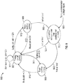
- Fig. 1 is a functional block diagram of a wireless power transfer system 100, in accordance with an illustrative embodiment.
- Input power 102 may be provided to a transmitter 104 from a power source (not shown in this figure) to generate a wireless (e.g., magnetic or electromagnetic) field 105 for performing energy transfer.
- a receiver 108 may couple to the wireless field 105 and generate output power 110 for storing or consumption by a device (not shown in this figure) coupled to the output power 110.
- the transmitter 104 and the receiver 108 may be separated by a distance 112.
- the transmitter 104 may include a power transmitting element 114 for transmitting/coupling energy to the receiver 108.
- the receiver 108 may include a power receiving element 118 for receiving or capturing/coupling energy transmitted from the transmitter 104.
- the transmitter 104 and the receiver 108 may be configured according to a mutual resonant relationship.
- the resonant frequency of the receiver 108 and the resonant frequency of the transmitter 104 are substantially the same or very close, transmission losses between the transmitter 104 and the receiver 108 are reduced.
- wireless power transfer may be provided over larger distances.
- Resonant inductive coupling techniques may thus allow for improved efficiency and power transfer over various distances and with a variety of inductive power transmitting and receiving element configurations.
- the wireless field 105 may correspond to the "near field" of the transmitter 104 as will be further described below.
- the near-field may correspond to a region in which there are strong reactive fields resulting from the currents and charges in the power transmitting element 114 that minimally radiate power away from the power transmitting element 114.
- the near-field may correspond to a region that is within about one wavelength (or a fraction thereof) of the power transmitting element 114.
- efficient energy transfer may occur by coupling a large portion of the energy in the wireless field 105 to the power receiving element 118 rather than propagating most of the energy in an electromagnetic wave to the far field.
- the transmitter 104 may output a time varying magnetic (or electromagnetic) field with a frequency corresponding to the resonant frequency of the power transmitting element 114.
- the time varying magnetic (or electromagnetic) field may induce a current in the power receiving element 118.
- the power receiving element 118 is configured as a resonant circuit to resonate at the frequency of the power transmitting element 114, energy may be efficiently transferred.
- An alternating current (AC) signal induced in the power receiving element 118 may be rectified to produce a direct current (DC) signal that may be provided to charge or to power a load.
- AC alternating current
- DC direct current
- Fig. 2 is a functional block diagram of a wireless power transfer system 200, in accordance with another illustrative embodiment.
- the system 200 may include a transmitter 204 and a receiver 208.
- the transmitter 204 (also referred to herein as power transmitting unit, PTU) may include transmit circuitry 206 that may include an oscillator 222, a driver circuit 224, a front-end circuit 226, and an impedance control module 227.
- the oscillator 222 may be configured to generate a signal at a desired frequency that may adjust in response to a frequency control signal 223.
- the oscillator 222 may provide the oscillator signal to the driver circuit 224.
- the driver circuit 224 may be configured to drive the power transmitting element 214 at, for example, a resonant frequency of the power transmitting element 214 based on an input voltage signal (VD) 225.
- the driver circuit 224 may be a switching amplifier configured to receive a square wave from the oscillator 222 and output a sine wave.
- the front-end circuit 226 may include a filter circuit to filter out harmonics or other unwanted frequencies.
- the front-end circuit 226 may include a matching circuit to match the impedance of the transmitter 204 to the power transmitting element 214.
- the front-end circuit 226 may include a tuning circuit to create a resonant circuit with the power transmitting element 214.
- the power transmitting element 214 may generate a wireless field 205 to wirelessly output power at a level sufficient for charging a battery 236, or otherwise powering a load.
- the impedance control module 227 may control the front-end circuit 226.
- the transmitter 204 may further include a controller 240 operably coupled to the transmit circuitry 206 configured to control one or aspects of the transmit circuitry 206 or accomplish other operations relevant to managing the transfer of power.
- the controller 240 may be a micro-controller or a processor.
- the controller 240 may be implemented as an application-specific integrated circuit (ASIC).
- ASIC application-specific integrated circuit
- the controller 240 may be operably connected, directly or indirectly, to each component of the transmit circuitry 206.
- the controller 240 may be further configured to receive information from each of the components of the transmit circuitry 206 and perform calculations based on the received information.
- the controller 240 may be configured to generate control signals (e.g., signal 223) for each of the components that may adjust the operation of that component.
- the controller 240 may be configured to adjust or manage the power transfer based on a result of the operations performed by it.
- the transmitter 204 may further include a memory (not shown) configured to store data, for example, such as instructions for causing the controller 240 to perform particular functions, such as those related to management of wireless power transfer.
- the receiver 208 may include receive circuitry 210 that may include a front-end circuit 232 and a rectifier circuit 234.
- the front-end circuit 232 may include matching circuitry to match the impedance of the receive circuitry 210 to the power receiving element 218.
- the front-end circuit 232 may further include a tuning circuit to create a resonant circuit with the power receiving element 218.
- the rectifier circuit 234 may generate a DC power output from an AC power input to charge the battery 236, as shown in Fig. 2 .
- the receiver 208 and the transmitter 204 may additionally communicate on a separate communication channel 219 (e.g., Bluetooth, Zigbee, cellular, etc.).
- the receiver 208 and the transmitter 204 may alternatively communicate via in-band signaling using characteristics of the wireless field 205.
- the receiver 208 may be configured to determine whether an amount of power transmitted by the transmitter 204 and received by the receiver 208 is appropriate for charging the battery 236.
- Transmitter 204 may be configured to generate a predominantly non-radiative field with a direct field coupling coefficient (k) for providing energy transfer.
- Receiver 208 may directly couple to the wireless field 205 and may generate an output power for storing or consumption by a battery (or load) 236 coupled to the output or receive circuitry 210.
- the receiver 208 may further include a controller 250 configured similarly to the transmit controller 240 as described above for managing one or more aspects of the wireless power receiver.
- the receiver 208 may further include a memory (not shown) configured to store data, for example, such as instructions for causing the controller 250 to perform particular functions, such as those related to management of wireless power transfer.
- transmitter 204 and receiver 208 may be separated by a distance and may be configured according to a mutual resonant relationship to minimize transmission losses between the transmitter and the receiver.
- Fig. 3 is a schematic diagram of a portion of the transmit circuitry 206 or the receive circuitry 210 of Fig. 2 , in accordance with illustrative embodiments.
- transmit or receive circuitry 350 may include a power transmitting or receiving element 352 and a tuning circuit 360.
- the power transmitting or receiving element 352 may also be referred to or be configured as an antenna or a "loop" antenna.
- the term “antenna” generally refers to a component that may wirelessly output or receive energy for coupling to another "antenna.”
- the power transmitting or receiving element 352 may also be referred to herein or be configured as a "magnetic" antenna, or an induction coil, a resonator, or a portion of a resonator.
- the power transmitting or receiving element 352 may also be referred to as a coil or resonator of a type that is configured to wirelessly output or receive power.
- the power transmitting or receiving element 352 is an example of a "power transfer component" of a type that is configured to wirelessly output and/or receive power.
- the power transmitting or receiving element 352 may include an air core or a physical core such as a ferrite core (not shown in this figure).
- the resonant frequency of the power transmitting or receiving element 352 may be based on the inductance and capacitance.
- Inductance may be simply the inductance created by a coil or other inductor forming the power transmitting or receiving element 352.
- Capacitance e.g., a capacitor
- the tuning circuit 360 may comprise a capacitor 354 and a capacitor 356 may be added to the transmit and/or receive circuitry 350 to create a resonant circuit.
- the tuning circuit 360 may include other components to form a resonant circuit with the power transmitting or receiving element 352.
- the tuning circuit 360 may include a capacitor (not shown) placed in parallel between the two terminals of the circuitry 350. Still other designs are possible.
- the tuning circuit in the front-end circuit 226 may have the same design (e.g., 360) as the tuning circuit in front-end circuit 232. In other embodiments, the front-end circuit 226 may use a tuning circuit design different than in the front-end circuit 232.
- the signal 358 For power transmitting elements, the signal 358, with a frequency that substantially corresponds to the resonant frequency of the power transmitting or receiving element 352, may be an input to the power transmitting or receiving element 352.
- the signal 358 For power receiving elements, the signal 358, with a frequency that substantially corresponds to the resonant frequency of the power transmitting or receiving element 352, may be an output from the power transmitting or receiving element 352.
- resonant and non-resonant implementations e.g., resonant and non-resonant circuits for power transmitting or receiving elements and resonant and non-resonant systems).
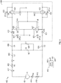
- FIG. 4 is a diagram of an exemplary power receiving element structure 400 that includes a synchronous rectifier 420.
- the power receiving element structure 400 comprises a voltage source 401, a resistance R5 402, a resistance R12 416, an inductor L2 403, capacitors C1 404, C2 405, C4 406, and C5 407.
- a voltage source 401 a voltage source 401
- a resistance R5 402 a resistance R12 416
- inductor L2 403 capacitors C1 404, C2 405, C4 406, and C5 407.
- the voltage source may have a sinusoidal voltage ranging from 0 to 4.243 V with a frequency of 6.78 MHz
- the resistance R5 402 may have a resistance of 667 m ⁇
- the resistance R12 416 may have a resistance of 1 ⁇
- the inductor L2 403 may have an inductance of 766 nH
- capacitors C1 404, C2 405, C4 406, and C5 407 may have a capacitance of 50 pF, 1 nF, 1 nF, and 150 pF respectively.
- the resistances shown in FIG. 4 may represent intrinsic resistances of components of the power receiving element structure 400 rather than separate resistances.
- the voltage source 401 merely is present to represent a time-varying induced voltage in response to an externally generated magnetic field during operation.
- a voltage across the voltage source may be measured at terminals "rx" 417 and "neg” 419.
- a resonant circuit of the power receiving element structure 400 may comprise the inductor L2 403 and capacitors C1 404 and C5 407.
- the power receiving element structure 400 also comprises the rectifier 420 that comprises diodes D1 421, D2 422, D3 423, and D4 424 (collectively, D1-D4) and switches S2 425, S3 426, S5 427, and S6 428 (collectively, S2-S3 and S5-S6).
- the power receiving element structure 400 may comprise a drive circuit 455 configured to actuate the switches via signals "dr" 440 and "drb" 441.
- the diodes D1-D4 represent actual diodes represent in the rectifier 420.
- the diodes D1-D4 represent body diodes of the switches S2-S3 and S5-S6.
- the rectifier 420 comprises a full bridge rectifier, in other aspects a half-bridge rectifier may be used.
- the switches S2-S3 and S5-S6 may comprise a transistor (e.g., MOSFET, JFET, etc.) or any other type of switch.
- the rectifier 420 may illustrate an exemplary configuration of the rectifier circuit 234 of FIG. 2 .
- the specific values described herein relating to the components of FIG. 4 are merely exemplary and non-limiting.
- synchronous rectification of the rectifier 420 can be obtained by operating the switches S2-S3 and S5-S6 in ZVS (zero voltage switching) at turn on and in ZCS (zero current switching) at turn off.
- the operation of the switches S2-S3 and S5-S6 may be timed and controlled to match the input signal from the voltage source 401.
- the turn off timing of the switches S2-S3 and S5-S6 may be varied or delayed to allow a reversal of the current in the switches S2-S3 and S5-S6.
- the current may initially flow into the load and for some time, prior to turn off, the current may flow from the load back into the resonating circuit (e.g., L2 403 and C1 404 and C5 407).
- the power receiving element 400 may control the output power to the load by adjusting the timing or thresholds of the switches S2-S3 and S5-S6.
- a receive circuit may be configured to receive wireless power via a magnetic field sufficient to power or charge a load and may generate an alternating current (AC) signal such as the voltage source 401.
- the rectifier 420 may be electrically coupled to the receive circuit and configured to rectify the AC signal generated in the receive circuit to a direct current (DC) signal for supplying power to the load.
- the rectifier 420 comprises a switch (e.g., S2-S3 and S5-S6) and the drive circuit 455 configured to actuate the switch when a current through the switch satisfies a non-zero current value.
- the non-zero current value is a threshold value that signals the drive circuit to open or close the switch.
- the non-zero current value is a negative current value such that the direction current flows from the load back into the receive circuit for a period of time before the switch is opened.
- the drive circuit may adjust the non-zero current value to adjust an output power to the load.
- the drive circuit adjusts a magnitude of the non-zero current value based on feedback from the load regarding a desired output power level.
- the drive circuit determines the non-zero current value is satisfied through a current sensor or a comparator coupled to the switch(es) (e.g., S2-S3 and S5-S6).
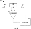
- FIG. 5 is a diagram of an exemplary switch circuitry 500 which may be included in the rectifier circuit 420 of FIG. 4 .
- the switch circuitry 500 comprises a switch S1 which has a parallel diode D1.
- the diode D1 may comprise a body diode of any MOS transistor.
- the switch circuitry 500 further comprises a comparator 550 across the switch S1 which compares a voltage of the terminals "rect" 501 and "out" 510 of the switch and a drive circuit 555 which sends a signal to the switch S1 to open or close the switch S1 when the voltage or current across the switch S1 reaches a threshold value.
- the drive circuit 555 sends the signal to the terminals "dr” 440 and/or "drb” 441 (See FIG. 4 ) to actuate or activate the corresponding switch (e.g., S2-S3 and S5-S6).
- the switches S2 425 and S3 426 (and corresponding diodes D2 422 and D3 423) of FIG. 4 may be replaced with the switch circuitry 500 which comprises the comparator 550 coupled to the drive circuit 555 which signals "dr" 440 and/or "drb” 441 to actuate the switches S2 425 and S3 426.
- the switches S5 427 and S6 428 may be replaced with the switch circuitry 500.
- the comparator 550 may send a signal to turn on the switch S1 (i.e., close the switch) when the voltages of the terminals rect 501 and out 510 are equal (e.g., ZVS). Additionally, the comparator 550 may send a signal to turn off the switch S1 (i.e., open the switch) when the current of the terminals rect 501 and out 510 are equal (e.g., ZCS).
- a hysteresis may be added to the comparator 550, so that the turn on of the switch S1 occurs when the voltage of terminal rect 501 is not zero.
- the hysteresis would be 30 mV.
- the comparator 550 determines that the voltage in the rect terminal 501 is 30 mV greater than the voltage of the out terminal 510 and signals the drive circuit 555 to turn on the switch S1. Accordingly, the switch S1 is turned on when the voltage across it is different than zero (non ZVS).
- a hysteresis e.g., -30 mV
- the switch S1 may be turned off when the current flowing through it is different than zero or a negative value.
- adding a hysteresis to the switch S1 may be equivalent to delaying the turn on or turn off of the switch S1, thus effectively shifting the phase of the current with respect to the phase of the voltage.
- the hysteresis implementation of FIG. 5 provides one mechanism for sensing current/adjusting threshold for controlling a switch.
- any type of current sensing circuit or other scheme may be used to sense the current through the switch S1 and determine how to adjust the timing of the switch S1 based on the current.
- the switch S1 may be coupled to a current sensor configured to sense a current through the switch. The sensor may be further configured to adjust the timing of the switched S1 based on the sensed current.
- the power receiving element 400 may comprise an output unit to measure a level of output power provided to the load.
- a controller of the power receiving element 400 or of the load may provide feedback to the rectifier 420.
- the feedback may comprise a desired level of power request or a difference between the output power and a desired output power.
- the rectifier or a controller may then determine how to adjust the timing of the switch(es) (e.g., S2-S3 and S5-6) or the hysteresis of the comparator 550 based on the feedback about the desired output power to be maintained or adjusted.
- the rectifier 420 or controller may then dynamically adjust the timing of the switches (e.g., S2-S3 and S5-6) threshold (hysteresis) based on the determined adjustment to either maintain the desired output power level or adjust the desired output power level.
- the switches e.g., S2-S3 and S5-6
- threshold hysteresis
- the effect of the hysteresis, or the adjustment of the timing of the switches may have an increased effect on the output power at induced voltages higher or equal to the output voltage than compared to resonant circuits operating at resonance.
- a tuning circuit e.g., tuning capacitor, transcap, variable capacitor, variable inductor, etc.
- the amount of power transferred to the load is decreased by increasing the hysteresis level.
- FIG. 6 is a diagram of an exemplary power receiving element 600 that includes a tuning circuit 610 and the rectifier circuit 420.
- the power receiving element 600 further comprises a resonant circuit 605, a battery or load 690, a driver circuit 625, a rectifier boost control circuit 630, a rectifier buck control circuit 640, and error amplifiers 631, 641, 651, and 652.
- the tuning circuit 610 may comprise a variable reactive element (e.g., tuning capacitor, transcap, variable capacitor, variable inductor, etc.).
- the tuning circuit 610 may be configured to detune the resonant circuit 605 away from resonance or tune the resonant circuit 605 closer to resonance.
- the tuning circuit 610 is configured to create a reactance shift of the resonant circuit 605.
- an impedance of the rectifier may be changed anywhere from close to zero (e.g., at resonance) to close to very negative (e.g., capacitive).
- the detuning of resonant circuit 605 may beneficially increase a range of output power control when used in combination with the tuning of the rectifier circuit 420 by adjusting the timing or thresholds of the rectifier circuit 420 switches (e.g., S2-S3 and S5-S6) described above.
- the adjustment of the timing or thresholds of the switches S2-S3 and S5-S6 may be controlled by the rectifier boost control circuit 630 and/or the rectifier buck control circuit 640.
- the rectifier boost control circuit 630 may be configured to increase the output power of the rectifier 420 beyond the tuning circuit 610 maximum value.
- the rectifier buck control circuit 640 may be configured to reduce the output power of the rectifier 420 beyond the tuning circuit 610 detuning capabilities.
- the power receiving element 600 receives certain inputs in order to determine which type of control to use to adjust induced voltage and/or output power.
- the error amplifier 651 receives as inputs a reference current (Iref1), a temperature input, and a resonator voltage input.
- Iref1 reference current
- the others are secondary inputs.
- the secondary inputs may become the limiting factor affecting the reference (typically reducing the reference value) only if the parameters assigned to the secondary inputs are above a given threshold.
- the error amplifier 651 determines and outputs a reference current (Iref) or a reference voltage (Vref, not shown) used by error amplifiers 631, 641, and 652 to determine the amount of tuning or delay control, if any, is needed.
- the fb signal refers to a feedback signal that, depending on the controlled parameter, can be a current, a voltage, a temperature, a resonant voltage, or other parameter feedback.
- the error amplifier 652 controls the tuning circuit 610 and the fb signal refers to a variable reactive element (e.g. variable capacitor) feedback.
- two or more of the error amplifiers 631, 641, and 652 may work concurrently. In other aspects, they may function separately.
- the error amplifiers 631, 641 and 652 generate an error signal such that their inputs (e.g., current or voltage) track each other, thus regulating the desired parameter.
- FIG. 7 is a chart 700 of exemplary values of output power and induced voltage and different tuning methods the power receiving element 600 may utilize based on output power and induced voltage values.
- Chart 700 shows values of induced voltage (e.g., voltage source 401) on the y-axis and values of output power (e.g., power to the battery 690).
- Chart 700 further shows a maximum induced voltage level 705, a minimum induced voltage level 710, a first output power level 720, and a second output power level 725, the second output power level 725 higher than the first output power level 720.
- the power receiving element 600 may utilize rectifier boost control to increase the induced voltage and/or the output power via the rectifier boost control circuit 630.
- the rectifier boost control circuit 630 and the rectifier 420 may boost or increase the induced voltage and/or the output power by adjusting the timing or thresholds of the switches S2-S3 and S5-S6.
- the power receiving element 600 may be operating in constant voltage mode and may wish to increase the output power to the battery 690.
- the rectifier boost control circuit 630 may reduce the hysteresis of turn off timing of the switches S2-S3 and S5-S6 so that less current from the battery 690 flows back into the resonant circuit 605 which may increase the output power.
- the power receiving element 600 may utilize rectifier buck control to reduce the induced voltage and/or the output power via the rectifier buck control circuit 640.
- the power receiving element 600 may be operating in constant voltage mode and may wish to reduce the output power to close to zero.
- rectifier buck control circuit 640 delays the turn off timing of the switches S2-S3 and S5-S6 which allows some current to flow back from the battery 690 to the resonant circuit 605 which may reduce the output power.
- the power receiving element 600 may utilize the tuning circuit 610 to control the induced voltage and/or output power of the rectifier 420.
- the tuning circuit 610 may be limited in the amount it may be able adjust the induced voltage and/or output power of the rectifier 402.
- the minimum value the tuning circuit 610 may adjust the rectifier 420 is illustrated at a point where the maximum induced voltage level 705 and the first output power level 720 intersect.
- the maximum value the tuning circuit 610 may adjust the rectifier 420 is illustrated at a point where the minimum induced voltage level 710 and the second output power level 725 intersect.
- the power receiving element 600 may be operating in a constant current charge mode illustrated between the first and second power levels 720 and 725.
- the tuning circuit 610 may adjust a value of a variable reactive element to maintain a constant current to the battery 690.
- the power receiving element may operate in a constant voltage mode (also referred to as trickle charge or beacon extension mode) between zero and the first power level 720.
- the rectifier 420 may adjust the timing or thresholds of the switches S2-S3 and S5-S6 to adjust the current and/or output power to maintain a constant voltage at the battery 690.
- rectifier buck and boost control occurs during the constant voltage mode.
- FIG. 8 is a chart 800 illustrating different output power control methods for different output power control levels.
- Chart 800 shows values of output power on the y-axis and time on the x-axis.
- FIG. 8 also shows a first output power level 805, represented by a horizontal dashed line, which represents a border of a range for values of output power that are capable of being tuned via the tuning circuit 610 or the rectifier buck control circuit 640.
- FIG. 8 further comprises a second output power level 810 above the first output power level 805 which represents a border of a range for values of output power that are capable of being tuned via the tuning circuit 610 or the rectifier boost control circuit 630.
- the first output power level 805 corresponds to the minimum output power level the tuning circuit 610 can tune the output power to.
- the second output power level 810 corresponds to the maximum output power level the tuning circuit 610 can tune the output power to.
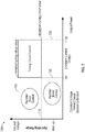
- FIG. 9 is a diagram 900 showing different states of voltage and output power control a power receiving element (e.g., power receiving element 600) may use for different power and voltage values.
- the diagram 900 may be implemented by the power receiving elements 400 or 600.
- the error amplifier 651 may receive inputs 901 of the resonant circuit 605, e.g., voltage, temperature, and/or current.
- the error amplifier 651 determines a current level (I ref ) or a voltage level (V ref ) of the resonant circuit 605 (e.g., outer loop of the power receiving element 600).
- the value of I ref and/or V ref may then be used to determine which type of control should be implemented.
- the value of I ref and/or V ref is output to each of a buck rectifier control state 906, a tuning circuit control state 907, and a boost rectifier control state 908 as shown by signals 903, 904, and 905, respectively.
- the buck rectifier control state 906 may include the rectifier buck control circuit 640 configured to adjust the timing or thresholds of the switches S2-S3 and S5-S6 to reduce a voltage level and/or output power level. Such a reduction may beyond a reduction capable by the tuning circuit 610.
- the rectifier buck control circuit 640 may adjust non-zero current value for the switch to turn off.
- the rectifier buck control circuit 640 may be configured to actuate one or more of the switches S2-S3 and S5-S6 when a current through the switch satisfies a non-zero current value.
- the rectifier buck control circuit 640 may adjust the non-zero current value from a first value to a second value, the second value being smaller than the first value.
- the non-zero current value may be adjusted from -5 mA to -200 mA. Such an adjustment increases the amount of current that flows from the battery 690 back into the resonant circuit 605 and reduces the output power.
- the power receiving element 600 may be operating in constant voltage mode and may wish to reduce the output power to close to zero.
- the turning circuit control state 907 via the tuning circuit 610 may only be able to reduce the output power to the first power level 720 (e.g., 1W) and the buck rectifier control state 906 may be used in conjunction with the tuning circuit control state 907 to further reduce the output power to close to zero.
- This combination of tuning control allows the power receiving element 600 to extend the range of output power control without significant efficiency loss. As shown in FIG.
- the power receiving element 600 may transition from using tuning circuit control 907 to the buck rectifier control state 906. For example as shown by transition 909, if the power receiving element 600 wishes to reduce a voltage or power level to beyond the tuning circuit control state 907 capabilities (e.g., close to 0V), it may transition to buck rectifier control state 906 to further reduce the voltage or power level. Similarly, the power receiving element 600 may transition from using the buck rectifier control state 906 to the tuning circuit control state 907.
- transition 910 when the buck rectifier control state 906 approaches 0V (e.g., no longer needs to reduce the voltage and/or power level), the power receiving element 600 transitions from the buck rectifier control state 906 to the tuning circuit control state 907 since the desired control is within the tuning circuit control state 907 capabilities.
- the power receiving element 600 may operate solely in the tuning circuit control state 907 via the tuning circuit 610.
- the tuning circuit 610 may adjust a value of a variable reactive component (e.g., tuning capacitor, transcap, variable capacitor, variable inductor, etc.) to adjust the output power within a certain range (e.g., between 1W and 1.7W).
- the power receiving element 600 may determine as shown at signal 911 whether the output power level or voltage level stays within the desired range, and if so, will continue using tuning circuit control state 907 to control tuning of the power receiving element 600.
- the boost rectifier control state 908 may include the rectifier boost control circuit 630 configured to adjust the timing or thresholds of the switches S2-S3 and S5-S6 to increase a voltage level and/or output power level. Such an increase may extend beyond an increase of the voltage and/or output power level capable by the tuning circuit 610. For example, if a voltage level of the battery 690 is close to the end of charge level, the power receiving element 600 may be operating in constant voltage mode and may wish to increase the output power to the battery 690. With reference to FIG.
- the tuning circuit control state 907 via the tuning circuit 610 may only be able to increase the output power to the from the first power level 720 to the second power level 725 (e.g., 1-1.7W) and the boost rectifier control state 908 may be used in conjunction with the tuning circuit control state 907 to further increase the capability of the power receiving element 600 to increase output power from values below the first power level 720 to values within the capabilities of the tuning circuit control state 907.
- This combination of tuning control allows the power receiving element to extend the range of output power control without significant efficiency loss. As shown in FIG.
- the power receiving element 600 may transition from the tuning circuit control state 907 to the boost rectifier control state 908 when it wishes to increase a voltage or power level to a level beyond the capabilities of the tuning circuit control state 907. For example as shown in transition 912, if the tuning circuit control state 907 approaches its maximum voltage level (e.g., 12V) and the power receiving element 600 or the battery 690 requests more power or voltage, then the power receiving element 600 will further utilize the boost rectifier control state 908 to increase the voltage/power level delivered to the load (e.g., battery 690).
- the load e.g., battery 690
- the power receiving element 600 may transition from the boost rectifier control state 908 to the tuning circuit control state 907 since the desired control is within the tuning circuit control state 907 capabilities.
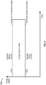
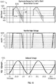
- FIG. 10 is a chart 1000 of exemplary outputs of a switch current, a rectifier input voltage, and an induced voltage for different hysteresis values.
- Chart 1000 comprises three different waveforms 1001-1003 for different hysteresis values ranging from 1 mV to 50 mV.
- the upper waveform 1001 represents the current in the switch (e.g., S2 of FIG. 4 ).
- the middle waveform 1002 represents the rectifier input voltage (e.g., voltage across terminals "rect” 430 and “rectb” 431 of FIG. 4 ).
- the lower waveform 1003 represents the induced voltage (e.g., voltage across terminals "rx" 417 and "neg” 419 of FIG. 4 ).
- the current at turn off reverses earlier (e.g., gets more negative) and the shift of the peak of the current with respect to the lower waveform 1003 (induced voltage waveform) decreases and moves more to the left.
- current (and power) is flowing from the load or battery (e.g., battery 236 of FIG. 2 ) back into the resonating circuit.
- curve 1010 of the upper waveform 1001 represents the current for the switch with a hysteresis of 1 mV and curve 1015 of the upper waveform represents the current for the switch with a hysteresis of 50 mV.
- the current through the switch S2 is approximately - 50 mA.
- the current through the switch S2 is approximately -450 mA.
- curve 1010 shows a peak current value of approximately 700 mA while curve 1015 shows a peak current value of approximately 550 mA.
- t 2 > t 1 which demonstrates the effective increased delay in turning off the switch S2 as the hysteresis is increased.
- adding a hysteresis effect or shifting the phase of the current of a rectifier as described above may have various effects depending on the conditions of the power receiving element 400 and on the rest of the resonating circuit.
- the capacitance value may be configured such that the resonant circuit of the power receiving element 400 is operating at resonance or very close to resonance. In that case, the impedance seen, looking into the rectifier, may be capacitive and the lower the induced voltage, the more capacitive the impedance.
- FIG. 11 is a chart 1100 showing exemplary outputs of a rectifier hysteresis, a battery current, an efficiency of the system, and an output power for different hysteresis values.
- Chart 1100 comprises four different waveforms 1101-1104 for these outputs when a hysteresis value of the comparator 550 changing from 20 mV to 70 mV.
- the upper waveform 1101 represents the hysteresis value of a comparator (e.g., comparator 550 of FIG. 5 ).
- the next lower waveform 1102 represents the current in the load or battery (e.g., battery 236 of FIG. 2 ).
- the next lower waveform 1103 represents the efficiency of the wireless power transfer system (e.g., wireless power transfer system 200 of FIG. 2 ).
- the bottom waveform 1104 represents the output power delivered to the load or battery (e.g., battery 236 of FIG. 2 ). As shown in chart 1100, when the hysteresis changes from 20 mV to 70 mV, the battery current and output power increases while the efficiency of the system decreases.
- system efficiency may decrease as a result of the increased hysteresis (e.g., inverse relationship)
- the decrease in efficiency is overcome by the benefits of the increased output power (e.g., for operating during a period of a low power beacon output from a transmitter for establishing a charging connection).
- the adjusting the hysteresis of the rectifier 420 may be accomplished by means of an analog loop, a separate controller, or by pulses to adjust a slope of change in the hysteresis. In other aspects, adjusting the hysteresis of the rectifier 420 or adjusting the timing of one or more of the switches S2-S3 and S5-S6 may be accomplished by any other means in accordance with the embodiments described herein.
- the phase shift from a hysteresis, or adjustment of the timing of one or more of the switches S2-S3 and S5-S6, may be negligible and the effect on the output power may be almost null as well.
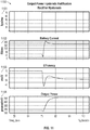
- FIG. 12 is a chart 1200 showing exemplary outputs of a dissipated power, a battery current, and an output power for different hysteresis values.
- Chart 1200 comprises three different waveforms 1201-1203 for these outputs for different hysteresis values ranging from 5 mV to 50 mV.
- the upper waveform 1201 represents a dissipated power in the system.
- the middle waveform 1202 represents the current in the load or battery (e.g., battery 236 of FIG. 2 ).
- the lower waveform 1203 represents the output power delivered to the load or battery (e.g., battery 236 of FIG. 2 ).
- curve 1210 shows an output power of approximately 1.7W for a hysteresis of 5 mV
- curve 1215 shows an output power of approximately 250mW for a hysteresis of 50 mV.
- the reduction of output power from 1.7W down to 250mW may be accomplished without dissipating a large amount of power.
- adjusting the switch timing or adding a hysteresis in a wireless power transfer system may have the benefit of extending the tuning effects both when more output power is desired (e.g., at low induced voltage levels) and when less power is desirable, as is the case of constant voltage mode of operation (e.g., at high induced voltage levels).
- this increased range of tuning may be cost-effective in that shifting the phase of the current does not require extra components and may reduce the cost of tuning resonant circuits.
- adjusting the switch timing or adding a hysteresis in a wireless power transfer system does not increase the voltage rating of the rectifier's elements nor of any other component.
- the control of the rectifier switches to adjust an output power described herein may be used to eliminate or reduce effects of component value variations due to tolerance of components.
- This rectifier control could also be used to control the output power with boot up induced voltage levels making the long beacon extension practical.
- This rectifier control could also be used to control the maximum voltage occurring at the resonator terminals.
- regulating output power levels via the rectifier 420 may allow for an implementation of a power receiving element without a DC-to-DC converter.
- the use of a hysteresis may have an effect on electromagnetic interference (EMI) and harmonic content.
- EMI electromagnetic interference
- the examples and embodiments discussed herein may also be extended to closed loop circuits.
- the examples and embodiments discussed herein may be applied to both resonant and non-resonant circuits and systems.
- FIG. 13 is a flowchart of an exemplary method 1300 of receiving wireless power, in accordance with the disclosure herein.
- the method shown in FIG. 13 may be implemented via one or more devices in the wireless power transfer system 100 similar to the power receiving element 118, the power receiving element 218, the receive circuitry 350, the power receiving element 400, the power receiving element 600, and the switch circuitry 500 of FIGs. 1-6 .
- the method 1300 is described herein with reference to a particular order, in various implementations, blocks herein may be performed in a different order, or omitted, and additional blocks may be added.
- the power receiving element receives, via a receive circuit, wireless power via a magnetic field sufficient to power or charge a load.
- the power receiving element detunes, via a tuning circuit comprising a variable reactive element and coupled to the receive circuit, the receive circuit away from a resonant frequency to achieve a first output power level based on a voltage level of the load.
- power receiving element rectifies, via a rectifier, an alternating current (AC) signal generated by the magnetic field to a direct current (DC) signal for supplying power to the load, the rectifier comprising a switch.
- the power receiving element actuates the switch when a current through the switch satisfies a first non-zero current value.
- the power receiving element adjusts the first non-zero current value to a second non-zero value to adjust the first output power level to a second output power level.
- any suitable means capable of performing the operations such as various hardware and/or software component(s), circuits, and/or module(s).
- any operations illustrated in the Figures may be performed by corresponding functional means capable of performing the operations.
- Information and signals may be represented using any of a variety of different technologies and techniques.
- data, instructions, commands, information, signals, bits, symbols, and chips that may be referenced throughout the above description may be represented by voltages, currents, electromagnetic waves, magnetic fields or particles, optical fields or particles, or any combination thereof.
- DSP Digital Signal Processor
- ASIC Application Specific Integrated Circuit
- FPGA Field Programmable Gate Array
- a general purpose processor may be a microprocessor, but in the alternative, the processor may be any conventional processor, controller, microcontroller, or state machine.
- a processor may also be implemented as a combination of computing devices, e.g., a combination of a DSP and a microprocessor, a plurality of microprocessors, one or more microprocessors in conjunction with a DSP core, or any other such configuration.
- a software module may reside in Random Access Memory (RAM), flash memory, Read Only Memory (ROM), Electrically Programmable ROM (EPROM), Electrically Erasable Programmable ROM (EEPROM), registers, hard disk, a removable disk, a CD ROM, or any other form of storage medium known in the art.
- RAM Random Access Memory
- ROM Read Only Memory
- EPROM Electrically Programmable ROM
- EEPROM Electrically Erasable Programmable ROM
- registers hard disk, a removable disk, a CD ROM, or any other form of storage medium known in the art.
- a storage medium is coupled to the processor such that the processor can read information from, and write information to, the storage medium.
- the storage medium may be integral to the processor.
- Disk and disc includes compact disc (CD), laser disc, optical disc, digital versatile disc (DVD), floppy disk and blu ray disc where disks usually reproduce data magnetically, while discs reproduce data optically with lasers. Combinations of the above should also be included within the scope of computer readable media.
- the processor and the storage medium may reside in an ASIC.
- the ASIC may reside in a user terminal.
- the processor and the storage medium may reside as discrete components in a user terminal.
Description
- This application is generally related to wireless power charging of chargeable devices, and more particularly for using synchronous rectifier control for adjusting output power.
- An increasing number and variety of electronic devices are powered via rechargeable batteries. Such devices include mobile phones, portable music players, laptop computers, tablet computers, computer peripheral devices, communication devices (e.g., Bluetooth devices), digital cameras, hearing aids, and the like. While battery technology has improved, battery-powered electronic devices increasingly require and consume greater amounts of power, thereby often requiring recharging. Rechargeable devices are often charged via wired connections through cables or other similar connectors that are physically connected to a power supply. Cables and similar connectors may sometimes be inconvenient or cumbersome and have other drawbacks. Wireless charging systems that are capable of transferring power in free space to be used to charge rechargeable electronic devices or provide power to electronic devices may overcome some of the deficiencies of wired charging solutions. As such, wireless power transfer systems and methods that efficiently and safely transfer power to electronic devices are desirable. An example of a wireless charging system is disclosed in
US2013033118 A1 . - Details of one or more implementations of the subject matter described in this specification are set forth in the accompanying drawings and the description below. Other features, aspects, and advantages will become apparent from the description, the drawings, and the claims. Note that the relative dimensions of the following figures may not be drawn to scale.
- According to the invention there is provided an apparatus for wirelessly receiving power according to
claim 1. - According to the invention there is also provided a method of receiving wireless power according to
claim 15. - Embodiments of the invention are disclosed in the dependent claims.
-
-
FIG. 1 is a functional block diagram of an exemplary wireless power transfer system, in accordance with exemplary embodiments. -
FIG. 2 is a functional block diagram of exemplary components that may be used in the wireless power transfer system ofFIG. 1 , in accordance with various exemplary embodiments. -
FIG. 3 is a schematic diagram of a portion of transmit circuitry or receive circuitry ofFIG. 2 including a transmit or receive antenna, in accordance with exemplary embodiments. -
FIG. 4 is a diagram of an exemplary power receiving element circuitry in accordance with an embodiment. -
FIG. 5 is a diagram of a portion of exemplary switch circuitry which may be used in the power receiving element ofFIG. 4 . -
FIG. 6 is a diagram of an exemplary power receiving element that includes a tuning circuit and a rectifier circuit. -
FIG. 7 is a chart of exemplary values of output power and induced voltage and different tuning methods a power receiving element may utilize based on the output power and induced voltage values -
FIG. 8 is a chart illustrating different output power control methods for different output power control levels. -
FIG. 9 is a diagram showing different states of voltage and output power control for different power and voltage values. -
FIG. 10 is a chart of exemplary outputs of a switch current, a rectifier input voltage, and an induced voltage for different hysteresis values. -
FIG. 11 is a chart showing exemplary outputs of a rectifier hysteresis, a battery current, an efficiency of the system, and an output power for different hysteresis values. -
FIG. 12 is a chart showing exemplary outputs of a dissipated power, a battery current, and an output power for different hysteresis values. -
FIG. 13 is a flowchart of an exemplary method of receiving wireless power, in accordance with the disclosure herein. - The various features illustrated in the drawings may not be drawn to scale. Accordingly, the dimensions of the various features may be arbitrarily expanded or reduced for clarity. In addition, some of the drawings may not depict all of the components of a given system, method or device. Finally, like reference numerals may be used to denote like features throughout the specification and figures.
- In the following description, for purposes of explanation, numerous examples and specific details are set forth in order to provide a thorough understanding of the present disclosure. It will be evident, however, to one skilled in the art that the present disclosure as expressed in the claims may include some or all of the features in these examples, alone or in combination with other features described below, and may further include modifications and equivalents of the features and concepts described herein.
- Wireless power transfer may refer to transferring any form of energy associated with electric fields, magnetic fields, electromagnetic fields, or otherwise from a transmitter to a receiver without the use of physical electrical conductors (e.g., power may be transferred through free space). The power output into a wireless field (e.g., a magnetic field or an electromagnetic field) may be received, captured by, or coupled by a "power receiving element" to achieve power transfer.
-
Fig. 1 is a functional block diagram of a wirelesspower transfer system 100, in accordance with an illustrative embodiment.Input power 102 may be provided to atransmitter 104 from a power source (not shown in this figure) to generate a wireless (e.g., magnetic or electromagnetic) field 105 for performing energy transfer. Areceiver 108 may couple to the wireless field 105 and generateoutput power 110 for storing or consumption by a device (not shown in this figure) coupled to theoutput power 110. Thetransmitter 104 and thereceiver 108 may be separated by adistance 112. Thetransmitter 104 may include a power transmittingelement 114 for transmitting/coupling energy to thereceiver 108. Thereceiver 108 may include a power receivingelement 118 for receiving or capturing/coupling energy transmitted from thetransmitter 104. - In one illustrative embodiment, the
transmitter 104 and thereceiver 108 may be configured according to a mutual resonant relationship. When the resonant frequency of thereceiver 108 and the resonant frequency of thetransmitter 104 are substantially the same or very close, transmission losses between thetransmitter 104 and thereceiver 108 are reduced. As such, wireless power transfer may be provided over larger distances. Resonant inductive coupling techniques may thus allow for improved efficiency and power transfer over various distances and with a variety of inductive power transmitting and receiving element configurations. - In certain embodiments, the wireless field 105 may correspond to the "near field" of the
transmitter 104 as will be further described below. The near-field may correspond to a region in which there are strong reactive fields resulting from the currents and charges in the power transmittingelement 114 that minimally radiate power away from the power transmittingelement 114. The near-field may correspond to a region that is within about one wavelength (or a fraction thereof) of the power transmittingelement 114. - In certain embodiments, efficient energy transfer may occur by coupling a large portion of the energy in the wireless field 105 to the
power receiving element 118 rather than propagating most of the energy in an electromagnetic wave to the far field. - In certain implementations, the
transmitter 104 may output a time varying magnetic (or electromagnetic) field with a frequency corresponding to the resonant frequency of the power transmittingelement 114. When thereceiver 108 is within the wireless field 105, the time varying magnetic (or electromagnetic) field may induce a current in the power receivingelement 118. As described above, if the power receivingelement 118 is configured as a resonant circuit to resonate at the frequency of the power transmittingelement 114, energy may be efficiently transferred. An alternating current (AC) signal induced in thepower receiving element 118 may be rectified to produce a direct current (DC) signal that may be provided to charge or to power a load. -
Fig. 2 is a functional block diagram of a wirelesspower transfer system 200, in accordance with another illustrative embodiment. Thesystem 200 may include atransmitter 204 and areceiver 208. The transmitter 204 (also referred to herein as power transmitting unit, PTU) may includetransmit circuitry 206 that may include anoscillator 222, adriver circuit 224, a front-end circuit 226, and animpedance control module 227. Theoscillator 222 may be configured to generate a signal at a desired frequency that may adjust in response to afrequency control signal 223. Theoscillator 222 may provide the oscillator signal to thedriver circuit 224. Thedriver circuit 224 may be configured to drive the power transmittingelement 214 at, for example, a resonant frequency of the power transmittingelement 214 based on an input voltage signal (VD) 225. Thedriver circuit 224 may be a switching amplifier configured to receive a square wave from theoscillator 222 and output a sine wave. - The front-
end circuit 226 may include a filter circuit to filter out harmonics or other unwanted frequencies. The front-end circuit 226 may include a matching circuit to match the impedance of thetransmitter 204 to thepower transmitting element 214. As will be explained in more detail below, the front-end circuit 226 may include a tuning circuit to create a resonant circuit with thepower transmitting element 214. As a result of driving thepower transmitting element 214, thepower transmitting element 214 may generate awireless field 205 to wirelessly output power at a level sufficient for charging abattery 236, or otherwise powering a load. Theimpedance control module 227 may control the front-end circuit 226. - The
transmitter 204 may further include acontroller 240 operably coupled to the transmitcircuitry 206 configured to control one or aspects of the transmitcircuitry 206 or accomplish other operations relevant to managing the transfer of power. Thecontroller 240 may be a micro-controller or a processor. Thecontroller 240 may be implemented as an application-specific integrated circuit (ASIC). Thecontroller 240 may be operably connected, directly or indirectly, to each component of the transmitcircuitry 206. Thecontroller 240 may be further configured to receive information from each of the components of the transmitcircuitry 206 and perform calculations based on the received information. Thecontroller 240 may be configured to generate control signals (e.g., signal 223) for each of the components that may adjust the operation of that component. As such, thecontroller 240 may be configured to adjust or manage the power transfer based on a result of the operations performed by it. Thetransmitter 204 may further include a memory (not shown) configured to store data, for example, such as instructions for causing thecontroller 240 to perform particular functions, such as those related to management of wireless power transfer. - The receiver 208 (also referred to herein as power receiving unit, PRU) may include receive circuitry 210 that may include a front-
end circuit 232 and arectifier circuit 234. The front-end circuit 232 may include matching circuitry to match the impedance of the receive circuitry 210 to thepower receiving element 218. As will be explained below, the front-end circuit 232 may further include a tuning circuit to create a resonant circuit with thepower receiving element 218. Therectifier circuit 234 may generate a DC power output from an AC power input to charge thebattery 236, as shown inFig. 2 . Thereceiver 208 and thetransmitter 204 may additionally communicate on a separate communication channel 219 (e.g., Bluetooth, Zigbee, cellular, etc.). Thereceiver 208 and thetransmitter 204 may alternatively communicate via in-band signaling using characteristics of thewireless field 205. - The
receiver 208 may be configured to determine whether an amount of power transmitted by thetransmitter 204 and received by thereceiver 208 is appropriate for charging thebattery 236.Transmitter 204 may be configured to generate a predominantly non-radiative field with a direct field coupling coefficient (k) for providing energy transfer.Receiver 208 may directly couple to thewireless field 205 and may generate an output power for storing or consumption by a battery (or load) 236 coupled to the output or receive circuitry 210. - The
receiver 208 may further include acontroller 250 configured similarly to the transmitcontroller 240 as described above for managing one or more aspects of the wireless power receiver. Thereceiver 208 may further include a memory (not shown) configured to store data, for example, such as instructions for causing thecontroller 250 to perform particular functions, such as those related to management of wireless power transfer. - As discussed above,
transmitter 204 andreceiver 208 may be separated by a distance and may be configured according to a mutual resonant relationship to minimize transmission losses between the transmitter and the receiver. -
Fig. 3 is a schematic diagram of a portion of the transmitcircuitry 206 or the receive circuitry 210 ofFig. 2 , in accordance with illustrative embodiments. As illustrated inFig. 3 , transmit or receivecircuitry 350 may include a power transmitting or receivingelement 352 and atuning circuit 360. The power transmitting or receivingelement 352 may also be referred to or be configured as an antenna or a "loop" antenna. The term "antenna" generally refers to a component that may wirelessly output or receive energy for coupling to another "antenna." The power transmitting or receivingelement 352 may also be referred to herein or be configured as a "magnetic" antenna, or an induction coil, a resonator, or a portion of a resonator. The power transmitting or receivingelement 352 may also be referred to as a coil or resonator of a type that is configured to wirelessly output or receive power. As used herein, the power transmitting or receivingelement 352 is an example of a "power transfer component" of a type that is configured to wirelessly output and/or receive power. The power transmitting or receivingelement 352 may include an air core or a physical core such as a ferrite core (not shown in this figure). - When the power transmitting or receiving
element 352 is configured as a resonant circuit or resonator withtuning circuit 360, the resonant frequency of the power transmitting or receivingelement 352 may be based on the inductance and capacitance. Inductance may be simply the inductance created by a coil or other inductor forming the power transmitting or receivingelement 352. Capacitance (e.g., a capacitor) may be provided by thetuning circuit 360 to create a resonant structure at a desired resonant frequency. As a non-limiting example, thetuning circuit 360 may comprise acapacitor 354 and acapacitor 356 may be added to the transmit and/or receivecircuitry 350 to create a resonant circuit. - The
tuning circuit 360 may include other components to form a resonant circuit with the power transmitting or receivingelement 352. As another non-limiting example, thetuning circuit 360 may include a capacitor (not shown) placed in parallel between the two terminals of thecircuitry 350. Still other designs are possible. In some embodiments, the tuning circuit in the front-end circuit 226 may have the same design (e.g., 360) as the tuning circuit in front-end circuit 232. In other embodiments, the front-end circuit 226 may use a tuning circuit design different than in the front-end circuit 232. - For power transmitting elements, the
signal 358, with a frequency that substantially corresponds to the resonant frequency of the power transmitting or receivingelement 352, may be an input to the power transmitting or receivingelement 352. For power receiving elements, thesignal 358, with a frequency that substantially corresponds to the resonant frequency of the power transmitting or receivingelement 352, may be an output from the power transmitting or receivingelement 352. Embodiments and descriptions provided herein may be applied to resonant and non-resonant implementations (e.g., resonant and non-resonant circuits for power transmitting or receiving elements and resonant and non-resonant systems). -
FIG. 4 is a diagram of an exemplary power receivingelement structure 400 that includes asynchronous rectifier 420. As shown, the power receivingelement structure 400 comprises avoltage source 401, aresistance R5 402, aresistance R12 416, aninductor L2 403,capacitors C1 404,C2 405,C4 406, andC5 407. In the exemplary configuration shown inFIG. 4 , the voltage source may have a sinusoidal voltage ranging from 0 to 4.243 V with a frequency of 6.78 MHz, theresistance R5 402 may have a resistance of 667 mΩ, theresistance R12 416 may have a resistance of 1 µΩ, theinductor L2 403 may have an inductance of 766 nH,capacitors C1 404,C2 405,C4 406, andC5 407 may have a capacitance of 50 pF, 1 nF, 1 nF, and 150 pF respectively. In some aspects, the resistances shown inFIG. 4 may represent intrinsic resistances of components of the power receivingelement structure 400 rather than separate resistances. In some embodiments, thevoltage source 401 merely is present to represent a time-varying induced voltage in response to an externally generated magnetic field during operation. In some aspects, a voltage across the voltage source may be measured at terminals "rx" 417 and "neg" 419. In some aspects, a resonant circuit of the power receivingelement structure 400 may comprise theinductor L2 403 andcapacitors C1 404 andC5 407. The powerreceiving element structure 400 also comprises therectifier 420 that comprisesdiodes D1 421,D2 422,D3 423, and D4 424 (collectively, D1-D4) and switchesS2 425,S3 426,S5 427, and S6 428 (collectively, S2-S3 and S5-S6). In some embodiments, the power receivingelement structure 400 may comprise adrive circuit 455 configured to actuate the switches via signals "dr" 440 and "drb" 441. In some aspects, the diodes D1-D4 represent actual diodes represent in therectifier 420. In some aspects, the diodes D1-D4 represent body diodes of the switches S2-S3 and S5-S6. While therectifier 420 comprises a full bridge rectifier, in other aspects a half-bridge rectifier may be used. The switches S2-S3 and S5-S6 may comprise a transistor (e.g., MOSFET, JFET, etc.) or any other type of switch. In some embodiments, therectifier 420 may illustrate an exemplary configuration of therectifier circuit 234 ofFIG. 2 . The specific values described herein relating to the components ofFIG. 4 are merely exemplary and non-limiting. - In some embodiments, synchronous rectification of the
rectifier 420 can be obtained by operating the switches S2-S3 and S5-S6 in ZVS (zero voltage switching) at turn on and in ZCS (zero current switching) at turn off. When using therectifier 420, the operation of the switches S2-S3 and S5-S6 may be timed and controlled to match the input signal from thevoltage source 401. - In some embodiments, it may be beneficial to adjust the operation of the switches S2-S3 and S5-S6 such that the switches no longer operate at ZVS and/or ZCS. In particular, the turn off timing of the switches S2-S3 and S5-S6 may be varied or delayed to allow a reversal of the current in the switches S2-S3 and S5-S6. In such embodiments, the current may initially flow into the load and for some time, prior to turn off, the current may flow from the load back into the resonating circuit (e.g.,
L2 403 andC1 404 and C5 407). This delay at turn off of the switches S2-S3 and S5-S6 may cause a change of effective impedance as seen looking into the rectifier and a shift of the current phase. In some aspects, for example if implemented in a closed loop embodiment, thepower receiving element 400 may control the output power to the load by adjusting the timing or thresholds of the switches S2-S3 and S5-S6. - For example, in some embodiments a receive circuit may be configured to receive wireless power via a magnetic field sufficient to power or charge a load and may generate an alternating current (AC) signal such as the
voltage source 401. Therectifier 420 may be electrically coupled to the receive circuit and configured to rectify the AC signal generated in the receive circuit to a direct current (DC) signal for supplying power to the load. Therectifier 420 comprises a switch (e.g., S2-S3 and S5-S6) and thedrive circuit 455 configured to actuate the switch when a current through the switch satisfies a non-zero current value. In some aspects, the non-zero current value is a threshold value that signals the drive circuit to open or close the switch. In some aspects, the non-zero current value is a negative current value such that the direction current flows from the load back into the receive circuit for a period of time before the switch is opened. The drive circuit may adjust the non-zero current value to adjust an output power to the load. In some aspects, the drive circuit adjusts a magnitude of the non-zero current value based on feedback from the load regarding a desired output power level. In some aspects, the drive circuit determines the non-zero current value is satisfied through a current sensor or a comparator coupled to the switch(es) (e.g., S2-S3 and S5-S6). -
FIG. 5 is a diagram of anexemplary switch circuitry 500 which may be included in therectifier circuit 420 ofFIG. 4 . As shown inFIG. 5 , theswitch circuitry 500 comprises a switch S1 which has a parallel diode D1. The diode D1 may comprise a body diode of any MOS transistor. Theswitch circuitry 500 further comprises acomparator 550 across the switch S1 which compares a voltage of the terminals "rect" 501 and "out" 510 of the switch and adrive circuit 555 which sends a signal to the switch S1 to open or close the switch S1 when the voltage or current across the switch S1 reaches a threshold value. In some embodiments, thedrive circuit 555 sends the signal to the terminals "dr" 440 and/or "drb" 441 (SeeFIG. 4 ) to actuate or activate the corresponding switch (e.g., S2-S3 and S5-S6). For example, in some aspects theswitches S2 425 and S3 426 (andcorresponding diodes D2 422 and D3 423) ofFIG. 4 may be replaced with theswitch circuitry 500 which comprises thecomparator 550 coupled to thedrive circuit 555 which signals "dr" 440 and/or "drb" 441 to actuate theswitches S2 425 andS3 426. In other aspects, theswitches S5 427 and S6 428 (andcorresponding diodes D1 421 and D4 424) may be replaced with theswitch circuitry 500. As described above, in a synchronous rectifier circuit, thecomparator 550 may send a signal to turn on the switch S1 (i.e., close the switch) when the voltages of the terminals rect 501 and out 510 are equal (e.g., ZVS). Additionally, thecomparator 550 may send a signal to turn off the switch S1 (i.e., open the switch) when the current of the terminals rect 501 and out 510 are equal (e.g., ZCS). - As described above, it may be desirable to adjust the operation of the switch S1 to adjust an output power delivered to the load (e.g.,
battery 236 ofFIG. 2 ). For example, a hysteresis may be added to thecomparator 550, so that the turn on of the switch S1 occurs when the voltage ofterminal rect 501 is not zero. In some aspects, the hysteresis comprises a threshold voltage or current for determining when or under what conditions to actuate the switch S1. For instance, a threshold that thecomparator 550 uses to turn on the switch S1 may occur when there is a 30 mV greater voltage in therect terminal 501 than the voltage of the out terminal 510 (i.e., Vrect - Vout = 30 mV). In this example, the hysteresis would be 30 mV. In some aspects, thecomparator 550 determines that the voltage in therect terminal 501 is 30 mV greater than the voltage of theout terminal 510 and signals thedrive circuit 555 to turn on the switch S1. Accordingly, the switch S1 is turned on when the voltage across it is different than zero (non ZVS). Similarly, a hysteresis (e.g., -30 mV) may be added such that the turn off of the switch S1 occurs when the voltage ofterminal rect 501 is smaller than the voltage of terminal out 510 (e.g., Vrect - Vout = -30 mV). Thus, the switch S1 may be turned off when the current flowing through it is different than zero or a negative value. - In some aspects, adding a hysteresis to the switch S1 may be equivalent to delaying the turn on or turn off of the switch S1, thus effectively shifting the phase of the current with respect to the phase of the voltage. The hysteresis implementation of
FIG. 5 provides one mechanism for sensing current/adjusting threshold for controlling a switch. In some aspects, any type of current sensing circuit or other scheme may be used to sense the current through the switch S1 and determine how to adjust the timing of the switch S1 based on the current. For example, in one aspect the switch S1 may be coupled to a current sensor configured to sense a current through the switch. The sensor may be further configured to adjust the timing of the switched S1 based on the sensed current. - In some aspects, the
power receiving element 400 may comprise an output unit to measure a level of output power provided to the load. In some aspects, a controller of thepower receiving element 400 or of the load may provide feedback to therectifier 420. In some aspects, the feedback may comprise a desired level of power request or a difference between the output power and a desired output power. In some aspects, the rectifier or a controller may then determine how to adjust the timing of the switch(es) (e.g., S2-S3 and S5-6) or the hysteresis of thecomparator 550 based on the feedback about the desired output power to be maintained or adjusted. As described above, therectifier 420 or controller may then dynamically adjust the timing of the switches (e.g., S2-S3 and S5-6) threshold (hysteresis) based on the determined adjustment to either maintain the desired output power level or adjust the desired output power level. - In other embodiments, when the resonant circuit of the
power receiving element 400 operates with a reactance shift by using a tuning circuit (e.g., tuning capacitor, transcap, variable capacitor, variable inductor, etc.), the effect of the hysteresis, or the adjustment of the timing of the switches, may have an increased effect on the output power at induced voltages higher or equal to the output voltage than compared to resonant circuits operating at resonance. As described above, at low induced voltages and without any significant reactance shift, the power to the load is increased by increasing the amount of hysteresis. In contrast, with higher induced voltages and a given reactance shift realized by the tuning circuit (e.g., transcap detuning), the amount of power transferred to the load (e.g.,battery 236 ofFIG. 2 ) is decreased by increasing the hysteresis level. -
FIG. 6 is a diagram of an exemplarypower receiving element 600 that includes atuning circuit 610 and therectifier circuit 420. Thepower receiving element 600 further comprises aresonant circuit 605, a battery orload 690, adriver circuit 625, a rectifierboost control circuit 630, a rectifierbuck control circuit 640, anderror amplifiers tuning circuit 610 may comprise a variable reactive element (e.g., tuning capacitor, transcap, variable capacitor, variable inductor, etc.). Thetuning circuit 610 may be configured to detune theresonant circuit 605 away from resonance or tune theresonant circuit 605 closer to resonance. In some embodiments, thetuning circuit 610 is configured to create a reactance shift of theresonant circuit 605. In some aspects, based of the reactance shift, an impedance of the rectifier may be changed anywhere from close to zero (e.g., at resonance) to close to very negative (e.g., capacitive). In some aspects, the detuning ofresonant circuit 605 may beneficially increase a range of output power control when used in combination with the tuning of therectifier circuit 420 by adjusting the timing or thresholds of therectifier circuit 420 switches (e.g., S2-S3 and S5-S6) described above. - In some embodiments, the adjustment of the timing or thresholds of the switches S2-S3 and S5-S6 may be controlled by the rectifier
boost control circuit 630 and/or the rectifierbuck control circuit 640. For example, the rectifierboost control circuit 630 may be configured to increase the output power of therectifier 420 beyond thetuning circuit 610 maximum value. Additionally, the rectifierbuck control circuit 640 may be configured to reduce the output power of therectifier 420 beyond thetuning circuit 610 detuning capabilities. - In some embodiments, the
power receiving element 600 receives certain inputs in order to determine which type of control to use to adjust induced voltage and/or output power. As shown inFIG. 6 , theerror amplifier 651 receives as inputs a reference current (Iref1), a temperature input, and a resonator voltage input. Typically, among these inputs there is a dominant one (for instance if the current is regulated, then there is a current reference) and the others are secondary inputs. The secondary inputs may become the limiting factor affecting the reference (typically reducing the reference value) only if the parameters assigned to the secondary inputs are above a given threshold. In the alternative, there could be a multiplexer in front of theerror amplifier 651 to select the proper parameter from time to time. In some aspects, theerror amplifier 651 then determines and outputs a reference current (Iref) or a reference voltage (Vref, not shown) used byerror amplifiers FIG. 6 , refers to a feedback signal that, depending on the controlled parameter, can be a current, a voltage, a temperature, a resonant voltage, or other parameter feedback. In some aspects, theerror amplifier 652 controls thetuning circuit 610 and the fb signal refers to a variable reactive element (e.g. variable capacitor) feedback. In some aspects, two or more of theerror amplifiers error amplifiers -
FIG. 7 is achart 700 of exemplary values of output power and induced voltage and different tuning methods thepower receiving element 600 may utilize based on output power and induced voltage values. Chart 700 shows values of induced voltage (e.g., voltage source 401) on the y-axis and values of output power (e.g., power to the battery 690). Chart 700 further shows a maximum inducedvoltage level 705, a minimum inducedvoltage level 710, a firstoutput power level 720, and a secondoutput power level 725, the secondoutput power level 725 higher than the firstoutput power level 720. - As shown in
FIG. 7 , at induced voltage levels close to or lower than the minimum inducedvoltage level 710, thepower receiving element 600 may utilize rectifier boost control to increase the induced voltage and/or the output power via the rectifierboost control circuit 630. For example, the rectifierboost control circuit 630 and therectifier 420 may boost or increase the induced voltage and/or the output power by adjusting the timing or thresholds of the switches S2-S3 and S5-S6. In one aspect, if a voltage level of thebattery 690 is close to the end of charge level, thepower receiving element 600 may be operating in constant voltage mode and may wish to increase the output power to thebattery 690. In one aspect, the rectifierboost control circuit 630 may reduce the hysteresis of turn off timing of the switches S2-S3 and S5-S6 so that less current from thebattery 690 flows back into theresonant circuit 605 which may increase the output power. - Additionally, at high induced voltage levels close to or above the maximum induced
voltage level 705, thepower receiving element 600 may utilize rectifier buck control to reduce the induced voltage and/or the output power via the rectifierbuck control circuit 640. For example, if thebattery 690 is nearing a full or end of charge (e.g., at high induced voltage levels), thepower receiving element 600 may be operating in constant voltage mode and may wish to reduce the output power to close to zero. In some aspects, rectifierbuck control circuit 640 delays the turn off timing of the switches S2-S3 and S5-S6 which allows some current to flow back from thebattery 690 to theresonant circuit 605 which may reduce the output power. Also shown inFIG. 7 , between the maximum inducedvoltage level 705 and the minimum induced voltage level 710 (e.g., the operating range), thepower receiving element 600 may utilize thetuning circuit 610 to control the induced voltage and/or output power of therectifier 420. - As described above, the
tuning circuit 610 may be limited in the amount it may be able adjust the induced voltage and/or output power of therectifier 402. The minimum value thetuning circuit 610 may adjust therectifier 420 is illustrated at a point where the maximum inducedvoltage level 705 and the firstoutput power level 720 intersect. The maximum value thetuning circuit 610 may adjust therectifier 420 is illustrated at a point where the minimum inducedvoltage level 710 and the secondoutput power level 725 intersect. Additionally, in a typical charging scenario, during the initial charging of thebattery 690, thepower receiving element 600 may be operating in a constant current charge mode illustrated between the first andsecond power levels tuning circuit 610 may adjust a value of a variable reactive element to maintain a constant current to thebattery 690. After a voltage level in thebattery 690 satisfies a threshold, the power receiving element may operate in a constant voltage mode (also referred to as trickle charge or beacon extension mode) between zero and thefirst power level 720. In constant voltage mode, therectifier 420 may adjust the timing or thresholds of the switches S2-S3 and S5-S6 to adjust the current and/or output power to maintain a constant voltage at thebattery 690. In some aspects, rectifier buck and boost control occurs during the constant voltage mode. -
FIG. 8 is achart 800 illustrating different output power control methods for different output power control levels. Chart 800 shows values of output power on the y-axis and time on the x-axis.FIG. 8 also shows a firstoutput power level 805, represented by a horizontal dashed line, which represents a border of a range for values of output power that are capable of being tuned via thetuning circuit 610 or the rectifierbuck control circuit 640.FIG. 8 further comprises a secondoutput power level 810 above the firstoutput power level 805 which represents a border of a range for values of output power that are capable of being tuned via thetuning circuit 610 or the rectifierboost control circuit 630. In some aspects, the firstoutput power level 805 corresponds to the minimum output power level thetuning circuit 610 can tune the output power to. In some aspects, the secondoutput power level 810 corresponds to the maximum output power level thetuning circuit 610 can tune the output power to. -
FIG. 9 is a diagram 900 showing different states of voltage and output power control a power receiving element (e.g., power receiving element 600) may use for different power and voltage values. In some embodiments, the diagram 900 may be implemented by thepower receiving elements state 902, theerror amplifier 651 may receiveinputs 901 of theresonant circuit 605, e.g., voltage, temperature, and/or current. In some embodiments, theerror amplifier 651 determines a current level (Iref) or a voltage level (Vref) of the resonant circuit 605 (e.g., outer loop of the power receiving element 600). The value of Iref and/or Vref may then be used to determine which type of control should be implemented. As described above with respect toFIG. 6 , the value of Iref and/or Vref is output to each of a buckrectifier control state 906, a tuningcircuit control state 907, and a boostrectifier control state 908 as shown bysignals - With reference to
FIGs. 6-7 , in some embodiments, the buckrectifier control state 906 may include the rectifierbuck control circuit 640 configured to adjust the timing or thresholds of the switches S2-S3 and S5-S6 to reduce a voltage level and/or output power level. Such a reduction may beyond a reduction capable by thetuning circuit 610. In some embodiments, the rectifierbuck control circuit 640 may adjust non-zero current value for the switch to turn off. For example, the rectifierbuck control circuit 640 may be configured to actuate one or more of the switches S2-S3 and S5-S6 when a current through the switch satisfies a non-zero current value. In some aspects, the rectifierbuck control circuit 640 may adjust the non-zero current value from a first value to a second value, the second value being smaller than the first value. For example, the non-zero current value may be adjusted from -5 mA to -200 mA. Such an adjustment increases the amount of current that flows from thebattery 690 back into theresonant circuit 605 and reduces the output power. - In another example, if the
battery 690 is nearing a full or end of charge (e.g., at high induced voltage levels), thepower receiving element 600 may be operating in constant voltage mode and may wish to reduce the output power to close to zero. With reference toFIG. 7 , the turningcircuit control state 907, via thetuning circuit 610 may only be able to reduce the output power to the first power level 720 (e.g., 1W) and the buckrectifier control state 906 may be used in conjunction with the tuningcircuit control state 907 to further reduce the output power to close to zero. This combination of tuning control allows thepower receiving element 600 to extend the range of output power control without significant efficiency loss. As shown inFIG. 9 , thepower receiving element 600 may transition from usingtuning circuit control 907 to the buckrectifier control state 906. For example as shown bytransition 909, if thepower receiving element 600 wishes to reduce a voltage or power level to beyond the tuningcircuit control state 907 capabilities (e.g., close to 0V), it may transition to buckrectifier control state 906 to further reduce the voltage or power level. Similarly, thepower receiving element 600 may transition from using the buckrectifier control state 906 to the tuningcircuit control state 907. For example as shown bytransition 910, when the buckrectifier control state 906 approaches 0V (e.g., no longer needs to reduce the voltage and/or power level), thepower receiving element 600 transitions from the buckrectifier control state 906 to the tuningcircuit control state 907 since the desired control is within the tuningcircuit control state 907 capabilities. - In some aspects, during a constant current mode, the
power receiving element 600 may operate solely in the tuningcircuit control state 907 via thetuning circuit 610. With reference toFIGs. 6-7 , in the tuningcircuit control state 907, thetuning circuit 610 may adjust a value of a variable reactive component (e.g., tuning capacitor, transcap, variable capacitor, variable inductor, etc.) to adjust the output power within a certain range (e.g., between 1W and 1.7W). Thepower receiving element 600 may determine as shown atsignal 911 whether the output power level or voltage level stays within the desired range, and if so, will continue using tuningcircuit control state 907 to control tuning of thepower receiving element 600. - With reference to
FIGs. 6-7 , in some embodiments, the boostrectifier control state 908 may include the rectifierboost control circuit 630 configured to adjust the timing or thresholds of the switches S2-S3 and S5-S6 to increase a voltage level and/or output power level. Such an increase may extend beyond an increase of the voltage and/or output power level capable by thetuning circuit 610. For example, if a voltage level of thebattery 690 is close to the end of charge level, thepower receiving element 600 may be operating in constant voltage mode and may wish to increase the output power to thebattery 690. With reference toFIG. 7 , the tuningcircuit control state 907, via thetuning circuit 610 may only be able to increase the output power to the from thefirst power level 720 to the second power level 725 (e.g., 1-1.7W) and the boostrectifier control state 908 may be used in conjunction with the tuningcircuit control state 907 to further increase the capability of thepower receiving element 600 to increase output power from values below thefirst power level 720 to values within the capabilities of the tuningcircuit control state 907. This combination of tuning control allows the power receiving element to extend the range of output power control without significant efficiency loss. As shown inFIG. 9 , thepower receiving element 600 may transition from the tuningcircuit control state 907 to the boostrectifier control state 908 when it wishes to increase a voltage or power level to a level beyond the capabilities of the tuningcircuit control state 907. For example as shown intransition 912, if the tuningcircuit control state 907 approaches its maximum voltage level (e.g., 12V) and thepower receiving element 600 or thebattery 690 requests more power or voltage, then thepower receiving element 600 will further utilize the boostrectifier control state 908 to increase the voltage/power level delivered to the load (e.g., battery 690). Similarly, when the boostrectifier control state 908 is no longer needed (e.g., boost voltage approaches zero as shown by transition 913), thepower receiving element 600 may transition from the boostrectifier control state 908 to the tuningcircuit control state 907 since the desired control is within the tuningcircuit control state 907 capabilities. -
FIG. 10 is achart 1000 of exemplary outputs of a switch current, a rectifier input voltage, and an induced voltage for different hysteresis values.Chart 1000 comprises three different waveforms 1001-1003 for different hysteresis values ranging from 1 mV to 50 mV. Theupper waveform 1001 represents the current in the switch (e.g., S2 ofFIG. 4 ). Themiddle waveform 1002 represents the rectifier input voltage (e.g., voltage across terminals "rect" 430 and "rectb" 431 ofFIG. 4 ). Thelower waveform 1003 represents the induced voltage (e.g., voltage across terminals "rx" 417 and "neg" 419 ofFIG. 4 ). As shown, as the hysteresis increases, the current at turn off reverses earlier (e.g., gets more negative) and the shift of the peak of the current with respect to the lower waveform 1003 (induced voltage waveform) decreases and moves more to the left. Thus, at the time of turning off the switch S2, current (and power) is flowing from the load or battery (e.g.,battery 236 ofFIG. 2 ) back into the resonating circuit. - For example,
curve 1010 of theupper waveform 1001 represents the current for the switch with a hysteresis of 1 mV andcurve 1015 of the upper waveform represents the current for the switch with a hysteresis of 50 mV. Incurve 1010, at time t1 when the switch S2 is turned off, the current through the switch S2 is approximately - 50 mA. Incurve 1015, at time t2 when the switch S2 is turned off, the current through the switch S2 is approximately -450 mA. Additionally,curve 1010 shows a peak current value of approximately 700 mA whilecurve 1015 shows a peak current value of approximately 550 mA. As shown, t2 > t1 which demonstrates the effective increased delay in turning off the switch S2 as the hysteresis is increased. - In some embodiments, adding a hysteresis effect or shifting the phase of the current of a rectifier as described above may have various effects depending on the conditions of the
power receiving element 400 and on the rest of the resonating circuit. At low induced voltage levels, and in particular when the output (e.g.,battery 236 ofFIG. 2 ) voltage is relatively high with respect to the induced voltage (battery voltage higher than the root-mean-square (rms) value of the induced voltage), if adjusting the output power by adjusting a timing of the switches described above is used in combination with the variable capacitor technology, the capacitance value may be configured such that the resonant circuit of thepower receiving element 400 is operating at resonance or very close to resonance. In that case, the impedance seen, looking into the rectifier, may be capacitive and the lower the induced voltage, the more capacitive the impedance. - At low induced voltages (with respect to the output voltage), increasing the hysteresis of a switch may increase the amount of output power to the load.
FIG. 11 is achart 1100 showing exemplary outputs of a rectifier hysteresis, a battery current, an efficiency of the system, and an output power for different hysteresis values.Chart 1100 comprises four different waveforms 1101-1104 for these outputs when a hysteresis value of thecomparator 550 changing from 20 mV to 70 mV. Theupper waveform 1101 represents the hysteresis value of a comparator (e.g.,comparator 550 ofFIG. 5 ). The nextlower waveform 1102 represents the current in the load or battery (e.g.,battery 236 ofFIG. 2 ). The nextlower waveform 1103 represents the efficiency of the wireless power transfer system (e.g., wirelesspower transfer system 200 ofFIG. 2 ). Thebottom waveform 1104 represents the output power delivered to the load or battery (e.g.,battery 236 ofFIG. 2 ). As shown inchart 1100, when the hysteresis changes from 20 mV to 70 mV, the battery current and output power increases while the efficiency of the system decreases. While system efficiency may decrease as a result of the increased hysteresis (e.g., inverse relationship), in some aspects the decrease in efficiency is overcome by the benefits of the increased output power (e.g., for operating during a period of a low power beacon output from a transmitter for establishing a charging connection). - In some aspects, the adjusting the hysteresis of the
rectifier 420 may be accomplished by means of an analog loop, a separate controller, or by pulses to adjust a slope of change in the hysteresis. In other aspects, adjusting the hysteresis of therectifier 420 or adjusting the timing of one or more of the switches S2-S3 and S5-S6 may be accomplished by any other means in accordance with the embodiments described herein. - In some embodiments, when the resonant circuit of the
power receiving element 400 is at resonance, and has an induced voltage higher or equal to the output voltage, the phase shift from a hysteresis, or adjustment of the timing of one or more of the switches S2-S3 and S5-S6, may be negligible and the effect on the output power may be almost null as well. -
FIG. 12 is achart 1200 showing exemplary outputs of a dissipated power, a battery current, and an output power for different hysteresis values.Chart 1200 comprises three different waveforms 1201-1203 for these outputs for different hysteresis values ranging from 5 mV to 50 mV. Theupper waveform 1201 represents a dissipated power in the system. Themiddle waveform 1202 represents the current in the load or battery (e.g.,battery 236 ofFIG. 2 ). Thelower waveform 1203 represents the output power delivered to the load or battery (e.g.,battery 236 ofFIG. 2 ). As shown inchart 1200, as the hysteresis increases, the current in the battery decreases and the output power decreases as shown inwaveforms waveform 1203, curve 1210 shows an output power of approximately 1.7W for a hysteresis of 5 mV andcurve 1215 shows an output power of approximately 250mW for a hysteresis of 50 mV. Additionally, as shown inwaveform 1201, the reduction of output power from 1.7W down to 250mW may be accomplished without dissipating a large amount of power. Thus, adjusting the switch timing or adding a hysteresis in a wireless power transfer system, may have the benefit of extending the tuning effects both when more output power is desired (e.g., at low induced voltage levels) and when less power is desirable, as is the case of constant voltage mode of operation (e.g., at high induced voltage levels). - Additionally, this increased range of tuning may be cost-effective in that shifting the phase of the current does not require extra components and may reduce the cost of tuning resonant circuits. Furthermore, adjusting the switch timing or adding a hysteresis in a wireless power transfer system does not increase the voltage rating of the rectifier's elements nor of any other component. In some embodiments, the control of the rectifier switches to adjust an output power described herein may be used to eliminate or reduce effects of component value variations due to tolerance of components. This rectifier control could also be used to control the output power with boot up induced voltage levels making the long beacon extension practical. This rectifier control could also be used to control the maximum voltage occurring at the resonator terminals. Moreover, regulating output power levels via the
rectifier 420 may allow for an implementation of a power receiving element without a DC-to-DC converter. - In some aspects, the use of a hysteresis may have an effect on electromagnetic interference (EMI) and harmonic content. The examples and embodiments discussed herein may also be extended to closed loop circuits. The examples and embodiments discussed herein may be applied to both resonant and non-resonant circuits and systems.
-
FIG. 13 is a flowchart of anexemplary method 1300 of receiving wireless power, in accordance with the disclosure herein. The method shown inFIG. 13 may be implemented via one or more devices in the wirelesspower transfer system 100 similar to thepower receiving element 118, thepower receiving element 218, the receivecircuitry 350, thepower receiving element 400, thepower receiving element 600, and theswitch circuitry 500 ofFIGs. 1-6 . Although themethod 1300 is described herein with reference to a particular order, in various implementations, blocks herein may be performed in a different order, or omitted, and additional blocks may be added. - At
block 1305, the power receiving element receives, via a receive circuit, wireless power via a magnetic field sufficient to power or charge a load. Atblock 1310, the power receiving element detunes, via a tuning circuit comprising a variable reactive element and coupled to the receive circuit, the receive circuit away from a resonant frequency to achieve a first output power level based on a voltage level of the load. Atblock 1315, power receiving element rectifies, via a rectifier, an alternating current (AC) signal generated by the magnetic field to a direct current (DC) signal for supplying power to the load, the rectifier comprising a switch. Atblock 1320, the power receiving element actuates the switch when a current through the switch satisfies a first non-zero current value. Atblock 1325, the power receiving element adjusts the first non-zero current value to a second non-zero value to adjust the first output power level to a second output power level. - The various operations of methods described above may be performed by any suitable means capable of performing the operations, such as various hardware and/or software component(s), circuits, and/or module(s). Generally, any operations illustrated in the Figures may be performed by corresponding functional means capable of performing the operations.
- Information and signals may be represented using any of a variety of different technologies and techniques. For example, data, instructions, commands, information, signals, bits, symbols, and chips that may be referenced throughout the above description may be represented by voltages, currents, electromagnetic waves, magnetic fields or particles, optical fields or particles, or any combination thereof.
- The various illustrative logical blocks, modules, circuits, and algorithm steps described in connection with the embodiments disclosed herein may be implemented as electronic hardware, computer software, or combinations of both. To clearly illustrate this interchangeability of hardware and software, various illustrative components, blocks, modules, circuits, and steps have been described above generally in terms of their functionality. Whether such functionality is implemented as hardware or software depends upon the particular application and design constraints imposed on the overall system. The described functionality may be implemented in varying ways for each particular application, but such implementation decisions should not be interpreted as causing a departure from the scope of the embodiments of the invention.
- The various illustrative blocks, modules, and circuits described in connection with the embodiments disclosed herein may be implemented or performed with a general purpose processor, a Digital Signal Processor (DSP), an Application Specific Integrated Circuit (ASIC), a Field Programmable Gate Array (FPGA) or other programmable logic device, discrete gate or transistor logic, discrete hardware components, or any combination thereof designed to perform the functions described herein. A general purpose processor may be a microprocessor, but in the alternative, the processor may be any conventional processor, controller, microcontroller, or state machine. A processor may also be implemented as a combination of computing devices, e.g., a combination of a DSP and a microprocessor, a plurality of microprocessors, one or more microprocessors in conjunction with a DSP core, or any other such configuration.
- The steps of a method or algorithm and functions described in connection with the embodiments disclosed herein may be embodied directly in hardware, in a software module executed by a processor, or in a combination of the two. If implemented in software, the functions may be stored on or transmitted over as one or more instructions or code on a tangible, non-transitory computer-readable medium. A software module may reside in Random Access Memory (RAM), flash memory, Read Only Memory (ROM), Electrically Programmable ROM (EPROM), Electrically Erasable Programmable ROM (EEPROM), registers, hard disk, a removable disk, a CD ROM, or any other form of storage medium known in the art. A storage medium is coupled to the processor such that the processor can read information from, and write information to, the storage medium. In the alternative, the storage medium may be integral to the processor. Disk and disc, as used herein, includes compact disc (CD), laser disc, optical disc, digital versatile disc (DVD), floppy disk and blu ray disc where disks usually reproduce data magnetically, while discs reproduce data optically with lasers. Combinations of the above should also be included within the scope of computer readable media. The processor and the storage medium may reside in an ASIC. The ASIC may reside in a user terminal. In the alternative, the processor and the storage medium may reside as discrete components in a user terminal.
- For purposes of summarizing the disclosure, certain aspects, advantages and novel features of the inventions have been described herein. It is to be understood that not necessarily all such advantages may be achieved in accordance with any particular embodiment of the invention. Thus, the invention may be embodied or carried out in a manner that achieves or optimizes one advantage or group of advantages as taught herein without necessarily achieving other advantages as may be taught or suggested herein.
Claims (15)
- An apparatus for wirelessly receiving power, the apparatus comprising:a receive circuit configured to receive wireless power via a magnetic field sufficient to power or charge a load;a tuning circuit (360,610) comprising a variable reactive element, coupled to the receive circuit, and configured to detune the receive circuit away from a resonant frequency to adjust an output power level to a first output power level; anda rectifier (420) electrically coupled to the receive circuit and configured to rectify an alternating current, AC, signal, generated in the receive circuit, to a direct current, DC signal for supplying power to the load (690), the rectifier comprising a switch (425,426, 427,428); anda drive circuitry (455; 550, 555)configured to:
measure a current through the switch and determine that the measured current satisfies a first non-zero current value;actuate the switch in response to the determination; andadjust the first non-zero current value to a second non-zero value to adjust the first output power level to a second output power level. - The apparatus of claim 1, wherein the variable reactive element comprises a variable capacitor.
- The apparatus of Claim 1, wherein the drive circuitry is further configured to actuate the switch based on a hysteresis effect and optionally wherein the hysteresis effect comprises a delay in turning off the switch.
- The apparatus of Claim 1, wherein the second non-zero current value is a negative current value such that a direction of the current flows from the load (690) into the receive circuit.
- The apparatus of Claim 1, wherein the drive circuitry further comprises a comparator (550) configured to measure the current through the switch and/or
a current sensor configured to sense the current through the switch. - The apparatus of Claim 1, wherein the first non-zero current value is lower than the second non-zero current value and the first output power level is lower than the second output power level.
- The apparatus of Claim 6, wherein a voltage generated in the receive circuit is less than a voltage level provided to the load (690).
- The apparatus of Claim 1, wherein the first non-zero current value is lower than the second non-zero current value and the first output power level is higher than the second output power level.
- The apparatus of Claim 8, wherein a voltage generated in the receive circuit is equal to or greater than a voltage level provided to the load (690).
- The apparatus of Claim 1, wherein the tuning circuit is further configured to generate a reactance shift in the receive circuit.
- The apparatus of Claim 1, wherein the second output power levelexceeds a power level the tuning circuit is capable of achieving.
- The apparatus of Claim 9, wherein the second output power level is lower than the first power level or wherein the second output power level is higher than the first output power level.
- The apparatus of Claim 1, wherein the tuning circuit is further configured to detune the receive circuit away from a resonant frequency to achieve a first output power level based on a reference voltage level or a reference current level of the receive circuit.
- The apparatus of Claim 11, wherein when the second output level is higher than the first output power level,the reference voltage level or the reference current level is based on one or more of a voltage, a temperature, and a current of the receive circuit.
- A method of receiving wireless power, comprising:Receiving (1305), via a receive circuit, wireless power via a magnetic field sufficient to power or charge a load (690);detuning (1310) via a variable reactive element coupled to the receive circuit, the receive circuit away from a resonant frequency to adjust an output power level to a first output power level;Rectifying (1315), via a rectifier, an alternating current AC signal generated by the magnetic field to a direct current, DC signal for supplying power to the load, the rectifier comprising a switch;measuring a current through the switch and determining that the measured current satisfies a first non-zero current value;actuating the switch in response to the determination; andadjusting (1325) the first non-zero current value to a second non-zero value to adjust the first output power level to a second output power level.
Applications Claiming Priority (3)
| Application Number | Priority Date | Filing Date | Title |
|---|---|---|---|
| US201562196865P | 2015-07-24 | 2015-07-24 | |
| US15/085,017 US10170937B2 (en) | 2015-07-24 | 2016-03-30 | Devices, systems, and methods for adjusting output power using synchronous rectifier control |
| PCT/US2016/041933 WO2017019294A1 (en) | 2015-07-24 | 2016-07-12 | Devices, systems, and methods for adjusting output power using synchronous rectifier control |
Publications (2)
| Publication Number | Publication Date |
|---|---|
| EP3326295A1 EP3326295A1 (en) | 2018-05-30 |
| EP3326295B1 true EP3326295B1 (en) | 2021-03-24 |
Family
ID=57836293
Family Applications (1)
| Application Number | Title | Priority Date | Filing Date |
|---|---|---|---|
| EP16744997.4A Active EP3326295B1 (en) | 2015-07-24 | 2016-07-12 | Device, and method for adjusting output power using synchronous rectifier control |
Country Status (7)
| Country | Link |
|---|---|
| US (1) | US10170937B2 (en) |
| EP (1) | EP3326295B1 (en) |
| JP (1) | JP6568300B2 (en) |
| KR (1) | KR102091950B1 (en) |
| CN (1) | CN107852197A (en) |
| BR (1) | BR112018001367A2 (en) |
| WO (1) | WO2017019294A1 (en) |
Families Citing this family (14)
| Publication number | Priority date | Publication date | Assignee | Title |
|---|---|---|---|---|
| US10129915B2 (en) * | 2016-05-27 | 2018-11-13 | Semiconductor Components Industries, Llc | Efficient closed loop tuning using signal strength |
| US10277059B2 (en) | 2017-04-24 | 2019-04-30 | Witricity Corporation | Wireless battery charger |
| US10348139B2 (en) | 2017-09-29 | 2019-07-09 | Witricity Corporation | Configurable wireless charging transmit and receive monitoring device |
| KR102087771B1 (en) * | 2018-01-31 | 2020-03-11 | 주식회사 지니틱스 | Synchronous rectifier adaptive to the frequency variation of wirelessly transferred input power |
| US20200328620A1 (en) * | 2018-02-19 | 2020-10-15 | Naptilus Technology Lab, S.L. | Tuner and rectifier circuit for wireless power receiver |
| CN109742863B (en) * | 2018-12-27 | 2023-06-20 | 华为技术有限公司 | Receiving end, transmitting end of wireless charging system and wireless charging system |
| US10998776B2 (en) | 2019-04-11 | 2021-05-04 | Apple Inc. | Wireless power system with in-band communications |
| CN110806778B (en) * | 2019-12-02 | 2020-09-18 | 中国美术学院 | Time base phase control direct current voltage stabilizing power supply |
| US11509229B2 (en) * | 2020-08-08 | 2022-11-22 | Patrick Carden | Resonant core power supply |
| KR20220020639A (en) * | 2020-08-12 | 2022-02-21 | 삼성전자주식회사 | An electronic device comprising a charging circuit |
| CN112217294B (en) * | 2020-08-19 | 2022-05-13 | 浙江大学 | Non-communication constant current control method applied to bidirectional wireless power transmission circuit |
| TWM607792U (en) * | 2020-11-20 | 2021-02-11 | 系統電子工業股份有限公司 | Tri-frequency trigger tool for tire pressure detection auxiliary system |
| US11949243B2 (en) * | 2020-12-17 | 2024-04-02 | Stmicroelectronics Design And Application S.R.O. | Apparatus and methods for enhanced operation in a wireless charging receiver |
| EP4040638B1 (en) * | 2021-02-04 | 2023-06-28 | Panthronics AG | Power adjustment in a non-regulated wireless charging system |
Family Cites Families (18)
| Publication number | Priority date | Publication date | Assignee | Title |
|---|---|---|---|---|
| JP4140169B2 (en) * | 2000-04-25 | 2008-08-27 | 松下電工株式会社 | Non-contact power transmission device |
| NZ525219A (en) * | 2003-04-09 | 2005-11-25 | Auckland Uniservices Ltd | Switchably decoupling resonant circuits utilised for controlling inductive power transfer from an alternating current source |
| JP4614961B2 (en) * | 2003-05-23 | 2011-01-19 | オークランド ユニサービシズ リミテッド | Method and apparatus for controlling an inductively coupled power transfer system |
| US20050288739A1 (en) * | 2004-06-24 | 2005-12-29 | Ethicon, Inc. | Medical implant having closed loop transcutaneous energy transfer (TET) power transfer regulation circuitry |
| US9782600B2 (en) * | 2009-08-20 | 2017-10-10 | Envoy Medical Corporation | Self-regulating transcutaneous energy transfer |
| US8374545B2 (en) | 2009-09-02 | 2013-02-12 | Qualcomm Incorporated | De-tuning in wireless power reception |
| US8300440B2 (en) | 2009-12-04 | 2012-10-30 | ConvenientPower HK Ltd. | AC-DC converter and AC-DC conversion method |
| CN103249592B (en) * | 2010-10-29 | 2016-06-15 | 高通股份有限公司 | For the method electric vehicle powered or charge and equipment |
| KR20140053282A (en) | 2011-08-04 | 2014-05-07 | 위트리시티 코포레이션 | Tunable wireless power architectures |
| US20130082538A1 (en) * | 2011-09-05 | 2013-04-04 | Peter Wambsganss | Circuitry And Method For Inductive Power Transmission |
| JP5702696B2 (en) | 2011-09-28 | 2015-04-15 | 株式会社アドバンテスト | Wireless power receiving device, wireless power feeding device, and wireless power feeding system |
| JP5868304B2 (en) | 2012-10-18 | 2016-02-24 | 株式会社アドバンテスト | Wireless power receiving apparatus, impedance control circuit usable in the same, and impedance control method |
| US9998180B2 (en) | 2013-03-13 | 2018-06-12 | Integrated Device Technology, Inc. | Apparatuses and related methods for modulating power of a wireless power receiver |
| US9685793B2 (en) | 2013-09-15 | 2017-06-20 | Glenn Gulak | Method and system for a complementary metal oxide semiconductor wireless power receiver |
| US20160308393A1 (en) | 2013-11-11 | 2016-10-20 | Powerbyproxi Limited | Contactless power receiver and method for operating same |
| CN105379137B (en) | 2014-01-08 | 2018-01-02 | 联发科技(新加坡)私人有限公司 | Radio source receiver with programmable power supply path |
| US9923381B2 (en) | 2014-03-04 | 2018-03-20 | Avago Technologies General Ip (Singapore) Pte. Ltd. | Resonant tuning through rectifier time shifting |
| US9755423B2 (en) | 2014-03-13 | 2017-09-05 | Infineon Technologies Ag | Overvoltage protection for a synchronous power rectifier |
-
2016
- 2016-03-30 US US15/085,017 patent/US10170937B2/en active Active
- 2016-07-12 JP JP2018502347A patent/JP6568300B2/en active Active
- 2016-07-12 WO PCT/US2016/041933 patent/WO2017019294A1/en active Application Filing
- 2016-07-12 KR KR1020187001870A patent/KR102091950B1/en active IP Right Grant
- 2016-07-12 EP EP16744997.4A patent/EP3326295B1/en active Active
- 2016-07-12 CN CN201680043315.1A patent/CN107852197A/en active Pending
- 2016-07-12 BR BR112018001367-6A patent/BR112018001367A2/en unknown
Non-Patent Citations (1)
| Title |
|---|
| None * |
Also Published As
| Publication number | Publication date |
|---|---|
| JP2018524966A (en) | 2018-08-30 |
| KR20180034411A (en) | 2018-04-04 |
| CN107852197A (en) | 2018-03-27 |
| KR102091950B1 (en) | 2020-03-20 |
| WO2017019294A1 (en) | 2017-02-02 |
| BR112018001367A2 (en) | 2018-09-11 |
| US20170025897A1 (en) | 2017-01-26 |
| EP3326295A1 (en) | 2018-05-30 |
| US10170937B2 (en) | 2019-01-01 |
| JP6568300B2 (en) | 2019-08-28 |
Similar Documents
| Publication | Publication Date | Title |
|---|---|---|
| EP3326295B1 (en) | Device, and method for adjusting output power using synchronous rectifier control | |
| EP3393002B1 (en) | Flexible bridge amplifier for wireless power | |
| US8111041B2 (en) | Power transmission control device, power reception control device, non-contact power transmission system, power transmission device, power reception device, and electronic instrument | |
| US10454306B2 (en) | Wireless power receiver and power control method thereof | |
| EP3469683B1 (en) | Device and method for controlling transmitter power supply based on wireless receiver request | |
| US9954581B2 (en) | Apparatuses and related methods for communication with a wireless power receiver | |
| US9904306B2 (en) | Voltage converter, wireless power reception device and wireless power transmission system including the same | |
| US10069340B2 (en) | Wireless power receiver for adjusting magnitude of wireless power | |
| EP2539991B1 (en) | Wireless power receiver | |
| US10491026B2 (en) | Impedance matching multiple coils in an electronic device | |
| US10075086B2 (en) | Inductive power transfer converters and system | |
| EP3479457B1 (en) | Apparatus and method for wireless power charging of subsequent receiver | |
| US10361581B2 (en) | Battery charger power control | |
| US9773609B2 (en) | Power supply apparatus and power control method thereof | |
| US20140177305A1 (en) | Gate drive circuit for synchronous rectification | |
| KR20140071233A (en) | Method and apparatus for charging control in wireless charge system | |
| US20170244254A1 (en) | Devices, systems, and methods for adjusting output power using synchronous rectifier control | |
| US20180219418A1 (en) | Methods and apparatus for efficient wireless power transfer | |
| KR102315924B1 (en) | Apparatus and method for wirless power transfer |
Legal Events
| Date | Code | Title | Description |
|---|---|---|---|
| STAA | Information on the status of an ep patent application or granted ep patent |
Free format text: STATUS: THE INTERNATIONAL PUBLICATION HAS BEEN MADE |
|
| PUAI | Public reference made under article 153(3) epc to a published international application that has entered the european phase |
Free format text: ORIGINAL CODE: 0009012 |
|
| STAA | Information on the status of an ep patent application or granted ep patent |
Free format text: STATUS: REQUEST FOR EXAMINATION WAS MADE |
|
| 17P | Request for examination filed |
Effective date: 20171206 |
|
| AK | Designated contracting states |
Kind code of ref document: A1 Designated state(s): AL AT BE BG CH CY CZ DE DK EE ES FI FR GB GR HR HU IE IS IT LI LT LU LV MC MK MT NL NO PL PT RO RS SE SI SK SM TR |
|
| AX | Request for extension of the european patent |
Extension state: BA ME |
|
| DAV | Request for validation of the european patent (deleted) | ||
| DAX | Request for extension of the european patent (deleted) | ||
| GRAP | Despatch of communication of intention to grant a patent |
Free format text: ORIGINAL CODE: EPIDOSNIGR1 |
|
| STAA | Information on the status of an ep patent application or granted ep patent |
Free format text: STATUS: GRANT OF PATENT IS INTENDED |
|
| RIC1 | Information provided on ipc code assigned before grant |
Ipc: H02M 7/219 20060101ALI20200608BHEP Ipc: H04B 5/00 20060101AFI20200608BHEP Ipc: H02J 7/02 20160101ALI20200608BHEP Ipc: H02J 50/80 20160101ALI20200608BHEP Ipc: H02M 3/335 20060101ALI20200608BHEP Ipc: H02J 7/00 20060101ALI20200608BHEP Ipc: H02M 7/48 20070101ALI20200608BHEP Ipc: H02J 50/12 20160101ALI20200608BHEP Ipc: H02M 1/00 20060101ALI20200608BHEP |
|
| INTG | Intention to grant announced |
Effective date: 20200713 |
|
| GRAJ | Information related to disapproval of communication of intention to grant by the applicant or resumption of examination proceedings by the epo deleted |
Free format text: ORIGINAL CODE: EPIDOSDIGR1 |
|
| STAA | Information on the status of an ep patent application or granted ep patent |
Free format text: STATUS: REQUEST FOR EXAMINATION WAS MADE |
|
| GRAP | Despatch of communication of intention to grant a patent |
Free format text: ORIGINAL CODE: EPIDOSNIGR1 |
|
| STAA | Information on the status of an ep patent application or granted ep patent |
Free format text: STATUS: GRANT OF PATENT IS INTENDED |
|
| INTC | Intention to grant announced (deleted) | ||
| INTG | Intention to grant announced |
Effective date: 20201215 |
|
| GRAS | Grant fee paid |
Free format text: ORIGINAL CODE: EPIDOSNIGR3 |
|
| GRAA | (expected) grant |
Free format text: ORIGINAL CODE: 0009210 |
|
| STAA | Information on the status of an ep patent application or granted ep patent |
Free format text: STATUS: THE PATENT HAS BEEN GRANTED |
|
| AK | Designated contracting states |
Kind code of ref document: B1 Designated state(s): AL AT BE BG CH CY CZ DE DK EE ES FI FR GB GR HR HU IE IS IT LI LT LU LV MC MK MT NL NO PL PT RO RS SE SI SK SM TR |
|
| REG | Reference to a national code |
Ref country code: GB Ref legal event code: FG4D |
|
| REG | Reference to a national code |
Ref country code: CH Ref legal event code: EP |
|
| REG | Reference to a national code |
Ref country code: IE Ref legal event code: FG4D |
|
| REG | Reference to a national code |
Ref country code: AT Ref legal event code: REF Ref document number: 1375560 Country of ref document: AT Kind code of ref document: T Effective date: 20210415 Ref country code: DE Ref legal event code: R096 Ref document number: 602016054826 Country of ref document: DE |
|
| REG | Reference to a national code |
Ref country code: LT Ref legal event code: MG9D |
|
| PG25 | Lapsed in a contracting state [announced via postgrant information from national office to epo] |
Ref country code: BG Free format text: LAPSE BECAUSE OF FAILURE TO SUBMIT A TRANSLATION OF THE DESCRIPTION OR TO PAY THE FEE WITHIN THE PRESCRIBED TIME-LIMIT Effective date: 20210624 Ref country code: HR Free format text: LAPSE BECAUSE OF FAILURE TO SUBMIT A TRANSLATION OF THE DESCRIPTION OR TO PAY THE FEE WITHIN THE PRESCRIBED TIME-LIMIT Effective date: 20210324 Ref country code: GR Free format text: LAPSE BECAUSE OF FAILURE TO SUBMIT A TRANSLATION OF THE DESCRIPTION OR TO PAY THE FEE WITHIN THE PRESCRIBED TIME-LIMIT Effective date: 20210625 Ref country code: FI Free format text: LAPSE BECAUSE OF FAILURE TO SUBMIT A TRANSLATION OF THE DESCRIPTION OR TO PAY THE FEE WITHIN THE PRESCRIBED TIME-LIMIT Effective date: 20210324 Ref country code: NO Free format text: LAPSE BECAUSE OF FAILURE TO SUBMIT A TRANSLATION OF THE DESCRIPTION OR TO PAY THE FEE WITHIN THE PRESCRIBED TIME-LIMIT Effective date: 20210624 |
|
| PG25 | Lapsed in a contracting state [announced via postgrant information from national office to epo] |
Ref country code: SE Free format text: LAPSE BECAUSE OF FAILURE TO SUBMIT A TRANSLATION OF THE DESCRIPTION OR TO PAY THE FEE WITHIN THE PRESCRIBED TIME-LIMIT Effective date: 20210324 Ref country code: RS Free format text: LAPSE BECAUSE OF FAILURE TO SUBMIT A TRANSLATION OF THE DESCRIPTION OR TO PAY THE FEE WITHIN THE PRESCRIBED TIME-LIMIT Effective date: 20210324 Ref country code: LV Free format text: LAPSE BECAUSE OF FAILURE TO SUBMIT A TRANSLATION OF THE DESCRIPTION OR TO PAY THE FEE WITHIN THE PRESCRIBED TIME-LIMIT Effective date: 20210324 |
|
| REG | Reference to a national code |
Ref country code: NL Ref legal event code: MP Effective date: 20210324 |
|
| REG | Reference to a national code |
Ref country code: AT Ref legal event code: MK05 Ref document number: 1375560 Country of ref document: AT Kind code of ref document: T Effective date: 20210324 |
|
| PG25 | Lapsed in a contracting state [announced via postgrant information from national office to epo] |
Ref country code: NL Free format text: LAPSE BECAUSE OF FAILURE TO SUBMIT A TRANSLATION OF THE DESCRIPTION OR TO PAY THE FEE WITHIN THE PRESCRIBED TIME-LIMIT Effective date: 20210324 |
|
| PG25 | Lapsed in a contracting state [announced via postgrant information from national office to epo] |
Ref country code: SM Free format text: LAPSE BECAUSE OF FAILURE TO SUBMIT A TRANSLATION OF THE DESCRIPTION OR TO PAY THE FEE WITHIN THE PRESCRIBED TIME-LIMIT Effective date: 20210324 Ref country code: AT Free format text: LAPSE BECAUSE OF FAILURE TO SUBMIT A TRANSLATION OF THE DESCRIPTION OR TO PAY THE FEE WITHIN THE PRESCRIBED TIME-LIMIT Effective date: 20210324 Ref country code: LT Free format text: LAPSE BECAUSE OF FAILURE TO SUBMIT A TRANSLATION OF THE DESCRIPTION OR TO PAY THE FEE WITHIN THE PRESCRIBED TIME-LIMIT Effective date: 20210324 Ref country code: CZ Free format text: LAPSE BECAUSE OF FAILURE TO SUBMIT A TRANSLATION OF THE DESCRIPTION OR TO PAY THE FEE WITHIN THE PRESCRIBED TIME-LIMIT Effective date: 20210324 Ref country code: EE Free format text: LAPSE BECAUSE OF FAILURE TO SUBMIT A TRANSLATION OF THE DESCRIPTION OR TO PAY THE FEE WITHIN THE PRESCRIBED TIME-LIMIT Effective date: 20210324 |
|
| PG25 | Lapsed in a contracting state [announced via postgrant information from national office to epo] |
Ref country code: RO Free format text: LAPSE BECAUSE OF FAILURE TO SUBMIT A TRANSLATION OF THE DESCRIPTION OR TO PAY THE FEE WITHIN THE PRESCRIBED TIME-LIMIT Effective date: 20210324 Ref country code: SK Free format text: LAPSE BECAUSE OF FAILURE TO SUBMIT A TRANSLATION OF THE DESCRIPTION OR TO PAY THE FEE WITHIN THE PRESCRIBED TIME-LIMIT Effective date: 20210324 Ref country code: PT Free format text: LAPSE BECAUSE OF FAILURE TO SUBMIT A TRANSLATION OF THE DESCRIPTION OR TO PAY THE FEE WITHIN THE PRESCRIBED TIME-LIMIT Effective date: 20210726 Ref country code: PL Free format text: LAPSE BECAUSE OF FAILURE TO SUBMIT A TRANSLATION OF THE DESCRIPTION OR TO PAY THE FEE WITHIN THE PRESCRIBED TIME-LIMIT Effective date: 20210324 Ref country code: IS Free format text: LAPSE BECAUSE OF FAILURE TO SUBMIT A TRANSLATION OF THE DESCRIPTION OR TO PAY THE FEE WITHIN THE PRESCRIBED TIME-LIMIT Effective date: 20210724 |
|
| REG | Reference to a national code |
Ref country code: DE Ref legal event code: R097 Ref document number: 602016054826 Country of ref document: DE |
|
| PG25 | Lapsed in a contracting state [announced via postgrant information from national office to epo] |
Ref country code: ES Free format text: LAPSE BECAUSE OF FAILURE TO SUBMIT A TRANSLATION OF THE DESCRIPTION OR TO PAY THE FEE WITHIN THE PRESCRIBED TIME-LIMIT Effective date: 20210324 Ref country code: AL Free format text: LAPSE BECAUSE OF FAILURE TO SUBMIT A TRANSLATION OF THE DESCRIPTION OR TO PAY THE FEE WITHIN THE PRESCRIBED TIME-LIMIT Effective date: 20210324 Ref country code: DK Free format text: LAPSE BECAUSE OF FAILURE TO SUBMIT A TRANSLATION OF THE DESCRIPTION OR TO PAY THE FEE WITHIN THE PRESCRIBED TIME-LIMIT Effective date: 20210324 |
|
| PLBE | No opposition filed within time limit |
Free format text: ORIGINAL CODE: 0009261 |
|
| STAA | Information on the status of an ep patent application or granted ep patent |
Free format text: STATUS: NO OPPOSITION FILED WITHIN TIME LIMIT |
|
| PG25 | Lapsed in a contracting state [announced via postgrant information from national office to epo] |
Ref country code: SI Free format text: LAPSE BECAUSE OF FAILURE TO SUBMIT A TRANSLATION OF THE DESCRIPTION OR TO PAY THE FEE WITHIN THE PRESCRIBED TIME-LIMIT Effective date: 20210324 |
|
| REG | Reference to a national code |
Ref country code: CH Ref legal event code: PL |
|
| 26N | No opposition filed |
Effective date: 20220104 |
|
| PG25 | Lapsed in a contracting state [announced via postgrant information from national office to epo] |
Ref country code: MC Free format text: LAPSE BECAUSE OF FAILURE TO SUBMIT A TRANSLATION OF THE DESCRIPTION OR TO PAY THE FEE WITHIN THE PRESCRIBED TIME-LIMIT Effective date: 20210324 |
|
| REG | Reference to a national code |
Ref country code: BE Ref legal event code: MM Effective date: 20210731 |
|
| PG25 | Lapsed in a contracting state [announced via postgrant information from national office to epo] |
Ref country code: LI Free format text: LAPSE BECAUSE OF NON-PAYMENT OF DUE FEES Effective date: 20210731 Ref country code: CH Free format text: LAPSE BECAUSE OF NON-PAYMENT OF DUE FEES Effective date: 20210731 |
|
| PG25 | Lapsed in a contracting state [announced via postgrant information from national office to epo] |
Ref country code: IS Free format text: LAPSE BECAUSE OF FAILURE TO SUBMIT A TRANSLATION OF THE DESCRIPTION OR TO PAY THE FEE WITHIN THE PRESCRIBED TIME-LIMIT Effective date: 20210724 Ref country code: LU Free format text: LAPSE BECAUSE OF NON-PAYMENT OF DUE FEES Effective date: 20210712 |
|
| PG25 | Lapsed in a contracting state [announced via postgrant information from national office to epo] |
Ref country code: IE Free format text: LAPSE BECAUSE OF NON-PAYMENT OF DUE FEES Effective date: 20210712 Ref country code: BE Free format text: LAPSE BECAUSE OF NON-PAYMENT OF DUE FEES Effective date: 20210731 |
|
| PG25 | Lapsed in a contracting state [announced via postgrant information from national office to epo] |
Ref country code: IT Free format text: LAPSE BECAUSE OF FAILURE TO SUBMIT A TRANSLATION OF THE DESCRIPTION OR TO PAY THE FEE WITHIN THE PRESCRIBED TIME-LIMIT Effective date: 20210324 |
|
| PG25 | Lapsed in a contracting state [announced via postgrant information from national office to epo] |
Ref country code: HU Free format text: LAPSE BECAUSE OF FAILURE TO SUBMIT A TRANSLATION OF THE DESCRIPTION OR TO PAY THE FEE WITHIN THE PRESCRIBED TIME-LIMIT; INVALID AB INITIO Effective date: 20160712 |
|
| PG25 | Lapsed in a contracting state [announced via postgrant information from national office to epo] |
Ref country code: CY Free format text: LAPSE BECAUSE OF FAILURE TO SUBMIT A TRANSLATION OF THE DESCRIPTION OR TO PAY THE FEE WITHIN THE PRESCRIBED TIME-LIMIT Effective date: 20210324 |
|
| PGFP | Annual fee paid to national office [announced via postgrant information from national office to epo] |
Ref country code: FR Payment date: 20230616 Year of fee payment: 8 |
|
| PGFP | Annual fee paid to national office [announced via postgrant information from national office to epo] |
Ref country code: GB Payment date: 20230614 Year of fee payment: 8 |
|
| PGFP | Annual fee paid to national office [announced via postgrant information from national office to epo] |
Ref country code: DE Payment date: 20230614 Year of fee payment: 8 |