EP3324548A1 - Bussystem und verfahren für fahrzeugsysteme - Google Patents
Bussystem und verfahren für fahrzeugsysteme Download PDFInfo
- Publication number
- EP3324548A1 EP3324548A1 EP16199250.8A EP16199250A EP3324548A1 EP 3324548 A1 EP3324548 A1 EP 3324548A1 EP 16199250 A EP16199250 A EP 16199250A EP 3324548 A1 EP3324548 A1 EP 3324548A1
- Authority
- EP
- European Patent Office
- Prior art keywords
- data
- bus
- unit
- processing units
- units
- Prior art date
- Legal status (The legal status is an assumption and is not a legal conclusion. Google has not performed a legal analysis and makes no representation as to the accuracy of the status listed.)
- Granted
Links
- 238000000034 method Methods 0.000 title claims description 13
- 238000012545 processing Methods 0.000 claims abstract description 32
- 230000005540 biological transmission Effects 0.000 claims description 18
- 230000010363 phase shift Effects 0.000 claims description 4
- 238000004891 communication Methods 0.000 description 6
- 238000013461 design Methods 0.000 description 5
- RYGMFSIKBFXOCR-UHFFFAOYSA-N Copper Chemical compound [Cu] RYGMFSIKBFXOCR-UHFFFAOYSA-N 0.000 description 4
- 230000008901 benefit Effects 0.000 description 4
- 239000010949 copper Substances 0.000 description 4
- 229910052802 copper Inorganic materials 0.000 description 4
- 239000000969 carrier Substances 0.000 description 3
- 239000000835 fiber Substances 0.000 description 3
- 230000002776 aggregation Effects 0.000 description 2
- 238000004220 aggregation Methods 0.000 description 2
- 238000013507 mapping Methods 0.000 description 2
- 230000008569 process Effects 0.000 description 2
- 230000011664 signaling Effects 0.000 description 2
- 238000001228 spectrum Methods 0.000 description 2
- 230000002457 bidirectional effect Effects 0.000 description 1
- 238000006243 chemical reaction Methods 0.000 description 1
- 238000011960 computer-aided design Methods 0.000 description 1
- 238000005265 energy consumption Methods 0.000 description 1
- 230000002093 peripheral effect Effects 0.000 description 1
- 150000003071 polychlorinated biphenyls Chemical class 0.000 description 1
- 230000002265 prevention Effects 0.000 description 1
- 230000009467 reduction Effects 0.000 description 1
- 230000004044 response Effects 0.000 description 1
- 238000012546 transfer Methods 0.000 description 1
- 230000001960 triggered effect Effects 0.000 description 1
Images


Classifications
-
- H—ELECTRICITY
- H04—ELECTRIC COMMUNICATION TECHNIQUE
- H04B—TRANSMISSION
- H04B3/00—Line transmission systems
- H04B3/54—Systems for transmission via power distribution lines
- H04B3/56—Circuits for coupling, blocking, or by-passing of signals
-
- B—PERFORMING OPERATIONS; TRANSPORTING
- B60—VEHICLES IN GENERAL
- B60R—VEHICLES, VEHICLE FITTINGS, OR VEHICLE PARTS, NOT OTHERWISE PROVIDED FOR
- B60R16/00—Electric or fluid circuits specially adapted for vehicles and not otherwise provided for; Arrangement of elements of electric or fluid circuits specially adapted for vehicles and not otherwise provided for
- B60R16/02—Electric or fluid circuits specially adapted for vehicles and not otherwise provided for; Arrangement of elements of electric or fluid circuits specially adapted for vehicles and not otherwise provided for electric constitutive elements
- B60R16/023—Electric or fluid circuits specially adapted for vehicles and not otherwise provided for; Arrangement of elements of electric or fluid circuits specially adapted for vehicles and not otherwise provided for electric constitutive elements for transmission of signals between vehicle parts or subsystems
Definitions
- This disclosure relates to vehicles systems and in particular to bus systems and communications methods for communicating data between processing units or systems of the vehicle, such as ECUs. It has particular but not exclusive application to communication between processing units of Advanced Driver Assistance Systems (ADAS) such as camera systems, radar systems, main ADAS control units and vehicle ECUs.
- ADAS Advanced Driver Assistance Systems
- ADAS Advanced driver assistance systems
- vehicle ECU vehicle ECU
- ADAS ADAS
- sub- ADAS
- ADAS system or function e.g. a camera serial interface (CSI) for cameras or Peripheral Component Interconnect (PCI)) express for external or internal high speed devices.
- CSI camera serial interface
- PCI Peripheral Component Interconnect
- Each bus may have several (e.g. parallel) high speed lines which have implicit limitations concerning for example signal routing and trace impedance. It is a difficult to provide bus systems meeting for all requirements when designing such vehicle architectures.
- Typical busses in automotive devices are: PCIe 2.0 / PCIe 3.0 (up to 8 lanes); HDMI 1.4; CSI II D-Phy (up to 4 lanes); GMSL; USB; 3.0 RGMII / SGMII / XGMII.
- PCIe 3.0 with eight lanes/lanes and is complex task also for state of the art Electronic Computer Aided Design (ECAD) .
- ECAD Electronic Computer Aided Design
- To route eight lanes means that there are eight connections of each two lines transmit and two lines of receive Additionally there are clock and control lines, which means that there can be typically up to 34 lines to route. Furthermore all lines need a controlled impedance and must preferably have the same length.
- a further disadvantage with current systems is that there is often there are several bus systems in whole architecture, which have to be are routed similarly (e.g. over a common connector).
- an on-board automotive system comprising a plurality of processing units adapted to transmit data between said processing units via a common bus, where one or more of said processing units has a convertor unit associated therewith, said convertor unit being connected to a parallel bus of the processing unit from which data is transmitted, said parallel bus comprising a plurality of lines, and wherein said converter is adapted to convert data transmitted therefrom to one or more of said processing units in the form of a single serial data stream along said common bus.
- Said common bus may include a single line for serial transmission of data therealong.
- One or more of said units may be an Electronic Control Unit.
- Said processing unit may be a main vehicle ECU.
- Said one or more of said processing units may be a radar and/or camera unit and/or Advanced Driver Assistance Systems (ADAS) unit.
- ADAS Advanced Driver Assistance Systems
- Said convertor unit may be adapted to modulate one or more carrier signals with the data to be transmitted.
- Said convertor unit may be adapted to modulate the data transmitted using one or more of the following transmission/modulation schemes: frequency division multiplexing (FDM); phase-shift keying (PSK); amplitude-shift keying (ASK); and quadrature amplitude modulation (QAM); and Orthogonal frequency-division multiplexing (OFDM).
- FDM frequency division multiplexing
- PSK phase-shift keying
- ASK amplitude-shift keying
- QAM quadrature amplitude modulation
- OFDM Orthogonal frequency-division multiplexing
- a method of transmitting data from a first processing unit of a vehicle to one or more other processing units of said vehicle comprising transmitting said data serially along a common bus, comprising the steps of:
- Said common bus may comprise or include a single line for serial transmission of data there along.
- One or more of said units is an Electronic Control Unit.
- Said processing unit may be a main vehicle ECU.
- Said one or more of said processing units may be a radar and/or camera unit and/or Advanced Driver Assistance Systems (ADAS) unit.
- ADAS Advanced Driver Assistance Systems
- Said converting step b) may include modulating one or more carrier signals with the data transmitted.
- Said modulation of data may use one or more of the following transmission/modulation schemes: frequency division multiplexing (FDM); phase-shift keying (PSK); amplitude-shift keying (ASK); and quadrature amplitude modulation (QAM):
- FDM frequency division multiplexing
- PSK phase-shift keying
- ASK amplitude-shift keying
- QAM quadrature amplitude modulation
- the problem of routing several busses (or bus types) in parallel is solved by using a common serial bus system which is connected to all processing units/ECUs/(sub-)systems of the vehicle architecture, and where data is transmitted serially.
- the problem of routing a lot of different signal lines is solved by using a single line for transmitting and a single line for receiving data or a single line for both receiving and transmitting data.
- data is transferred between vehicle processors/systems and ECUs using the same transmission scheme.
- the schemes may be varied and can similar to those used in mobile telecommunication systems.
- the bus system aggregates several high speed busses with a high pin count to only one common bus with one or two signal pairs (full-duplex or TX/RX pairs).
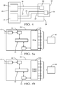
- Figure 1 shows prior art system architecture in a vehicle typically used for ADAS systems.
- the figure shows (sub-) systems 2, 3 and 4 of the architecture.
- system 2 may be regarded as a master system and sub-systems 3 and 4 regarded as slave systems.
- Each may be regarded as an ECU.
- the sub-system 2 may be the main vehicle ECU or control overall functionality, and subsystems 3 and 4 may be subsystems of an ADAS system. They can be manifested as integrated circuits i.e. chips or blocks of integrated circuits or modular circuit boards.
- Each system 2, 3, and 4 is connected directly to a connector 5 via buses 6, 7, and 8 respectively.
- the bus 7 may be a Reduced Gigabyte Media Independent Interface (RGMII), the, bus 8 may be a CSI-2.
- Subsystem 2 is connected by bus 9a to subsystem 3 and also to subsystem 4 by bus 9b.
- Bus 9a may be PCIe and bus 9b may be a USB 3.0.
- the buses each comprise several wires/lines each, and can be of varying types/designs. The inherent problems of such architecture are apparent.
- Figure 2 shows an example of the invention. Similar components have the same reference numeral as figure 1 .
- all the components subsystems 2, 3, 4, as well as connector 5 are connected to a serial common bus 10.
- the bus comprises a single line or a line pair as in the figure.
- the systems are connected to the single bus via convertor (intermediate) units 11,12, 13 such that data going to or from the subsystem is in the correct format/uses the same protocol/scheme for the serial data transmission system i.e. along bus 10.
- the convertor unit in examples, can also be regarded as a transmitter, receiver or transceiver unit; this will be described in more detail hereinafter. Generally they comprise modulator or demodulator means.
- Signals i.e. data out from a parallel bus of the system or processing unit are combined and then modulated for transmission and/or signals received by the converter are demodulated and then split (decombined) and forwarded on the appropriate lines of the parallel bus system of the (sub-)system or processing unit.
- buses 15 and 16 to the respective converter which may be a the same bus designs/types as any of buses 7, 8, 9a and 9b of figure 1 .
- bus 14 to the respective converter which is may again be any bus design.
- the convertor units thus act as interfaces between the common bus 10 and the other buses.
- the convertor units (and thus interfaces via respective buses 14,15 and 16) may be integral with the system i.e. on the same circuit board or part of the same integrated circuit as the system, as shown by the dotted line for system 2.
- the main advantage in the convertor unit being part of the system integrated circuit is better and easier signal routing on the PCB and therefore the reduction of engineering effort.
- the single common bus system may be used to connect two or more ECUs. This is shown in figure 3 where the main advantage is, that there is a big saving in cabling. High speed connections require dedicated cables (often coaxial) with expensive connectors and so each saving can reduce system costs.
- a first ECU/system 20 is connected to a second ECU/system 21 which is connected to a third ECU/system 22.
- This is via common serial bus 27 via e.g. a single link or as described above which may be a copper or fiber optic.
- the term "serial" bus again can be considered as a bus where data is transmitted and/or received along a single line. So the bus may comprise one line or two lines for respective transmission and reception.
- each ECU includes a microprocessor 24 and optionally one or more ECU sub-units/systems 25a and 25b, each of which is provided with a convertor 26.
- the convertor is shown integral with the ECU.
- Figure 4a and 4b illustrate a further application of aspects of the invention.
- Figure 4a shows a prior art ADAS system and figure 4b shows how this can be adapted according to one embodiment.
- Figure 4a shows an a Camera Unit 30 and Radar Unit 31 which may be considered part of an overall ADAS unit 35 connected to ADAS ECU 32.
- the ADAS ECU is divided into vision subsystem/ECU 33 and a radar subsystem/ECU 34.
- a dedicated high speed (data) output lines 36 are required, which connect respective units 30, 31 to units 33 and 34.
- data lines/ buses 37 are also provided, connecting units 30 and 31 with units 33 and 34 respectively.
- a power line 38 may be provided connected between the unit 32 and 35.
- the data connectivity is shown by two lines/buses 36 and 37 in practice these may comprise several lines each.
- Figure 4b shows an embodiment of the invention - similar component have the same reference numerals as figure 4a .
- Both the camera unit and the radar units/systems have their respective bus lines 36 and 37 connected to a convertor unit 39.
- This is then connected to the unit 32 via a high speed common serial bus 41 according to examples of the invention described above.
- This is connected to a converter unit 40 located as part of the ADAS ECU system 32.
- the converter unit is in turn connected to sub-units/systems 33 and 34.
- the converter unit units ensure that communications along bus 41 uses the protocol for the bus 41. So to summarise, in an example, all data and high speed busses of the prior art system of figure 4a are combined on a single very high speed bus.
- So camera and radar systems are connected via usual links (power data and high speed) to a common converter unit (transmitter /transceiver) 39 (alternatively each may have its own) which provides a modulated output on single or twin line bus 41 to the ADAS ECU.
- the converter units may provide functionality to convert data from different bus designs (for transmission or reception or both) for the common bus; in other words the converter units may have multiple functionality/conversion capability in this respect.
- the bus is universal and connects/communicates via the convertor essentially to any type of bus i.e. to a high variety of busses, used by systems which connects to the universal bus.
- an converter unit i.e. which may be a special (MAC/PHY) transceiver, which adapts the high speed (parallel) bus of the system to a serialized signal data stream (in respect of transmission reception or both) to be communicated on the serial common bus to allow access of the systems/units/ECUs to the bus.
- the converter unit (transceiver) can control the data flow on the bus and can control link quality. To connect more devices, it is possible to expand the bus with additional e.g.(MAC/PHY) transceivers.
- Each transceiver may have its own dedicated bus connection, for example a PCIe 2.0 or USB3.0 port. Each port may operates as a bidirectional input/output.
- Transceivers/converter units of a plurality (e.g. related) busses e.g. network: RGMII/SGMII
- RGMII/SGMII may implemented using a single integrated IC, which may be configurable.
- Figures 5a and 5b show convertor units (transmitters/transceivers) according to examples of the invention.
- Figure 5a shows a transceiver (converter unit) 40 (which could be used for units 40, 39, 26, 12, 13,14 of the previous figures) adapted to connect the serial universal bus 41 a (sub-)system 42 which utilizes in this example a PCIe bus system 45.
- the convertor unit/transceiver includes a central control unit 43 connected to MAC (Media Access Control) layer units 44 adapted to provide suitable communication for the common/serial bus line 41 and the PCIe bus respectively via connector 46 for the common bus and the 45 for the PCIe bus.
- Figure 5b shows a similar figure and arrangement or a RGMII and SGMII bus connection to system 48.
- the transceiver/converter unit can also be implemented in a system on chip (SoC) where an Field Programmable Gate Array (FPGA) or ASIC part in included.
- SoC system on chip
- FPGA Field Programmable Gate Array
- ASIC ASIC part in included.
- the bus according to examples can be implemented on a single PCB only, or used to connect to other PCBs to each other.
- the bus may be physically manifested by a copper cable or PCB trace or for higher data rates, may use a fiber optic link/cable. For higher data rates copper cable may also be utilized depending on requirements and configuration specification.
- the bus system and convertors units may use various protocols or data transmission schemes. Such schemes are used in wireless communication systems.
- OFDM Orthogonal Frequency-Division Multiplexing
- the payload on one single frequency is divided into a multiple of frequencies/carriers e.g. with small offset.
- the frequency, respectively the offset ( ⁇ f) is selected in this way, so that the harmonics have the lowest influence on adjacent frequencies. This is shown in figure 6 .
- payload data to be transmitted between units/system can be split into several frequencies for transmission along the common serial bus.
- the amount of different frequencies depends on the maximum available bandwidth of the channel and the desired frequency offset.
- N 1024 (but also 2048, 2 x is possible).
- Each subcarrier may contain one part of information of the payload.
- a modulation scheme is used.
- the 16-QAM Quadrature amplitude modulation
- Figure 7 shows a QAM symbol mapping.
- T the symbol duration of one Bit and N the total amount of sub carriers.
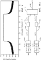
- Figure 9 shows a typical output spectrum of the converter unit/transmitter.
- the shown signal uses in maximum the bandwidth of 1GHz.
- Each entity in the final chip uses 1GHz of bandwidth, with an adjustable center frequency. With this behavior it is easy to cascade several of this units to one very high bandwidth combined channel. Also to achieve a full duplex architecture this fact is very helpful.
- the transmitters/convertor units can negotiate how to share and allocate the bunch of 1GHz sub channels. If there is low demand of a backchannel or in general of payload to transmit, the protocol can for instance reduce the modulation depth of the QAM system (do reduce bit errors / energy consumption / etc.) or re align the used frequency range to optimized bands (for example if there is EMI in some bands).
- busses can be: PCIe 2.0 / PCIe 3.0 up to 8 lanes; HDMI 1.4b; Sata; NVMe; Display Port (consumer /infotainment applications); CSI II D-Phy up to 4 lanes (CSI II); GMSL (2.0); LVDS; proprietary protocols for single line buses for; USB 3.0; RGMII / SGMII / XGMII / XAUI; CAN-FD; Flexray; GPIO; Ethernet (Time Triggered, TSN)
- each bus has its own characteristics.
- the PCIe 3.0 bus has several high speed differential data and clock lines, on the other hand a general purpose Low Voltage Differential Signaling (LVDS) signal consist only of one pair with undefined clock rate.
- LVDS Low Voltage Differential Signaling
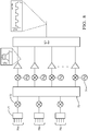
- Figure 10a and b shows transmitter/convertor hardware which enables data provided on one or more buses to be transmitted on a single line.
- this may form the adaptor/converter as described above.
- hardware used to transmit data from two bus types to be transmitted and combined along a single line. So it should be noted than in the figures, data from two buses /bus systems are transmitted to a single line or two lines) one for transmission one for reception); e.g. if a processor or ECU has two bus system outputs. It should be understood that the design can be simplified somewhat to transmit data only from a single bus system, or upgrades to provide an output from more than two bus systems.
- FIG. 10a Two portions of the transmitter/converter are shown in figures 10a and 10b .
- the input to the transmitter is from one or more individual (dedicated) buses/bus systems buses.
- the figure are shown inputs from two bus systems 50a and 50b.
- Each bus system may comprise a plurality of bus lines which may comprise e.g. 16 or 32 bus line or indeed may comprise any number of bus lines.
- each bus system is shown with three lines. Bus lines from buses 50a and 50b (with signals designated as s 1 (z) and s 2 (z)) are input to serialisers 51a and 51b respectively.
- the input designated generally s n (z) is input to respective combiner which collects all dedicated lines of each bus [s 11 (z)] to [s 1n (z)] or s 21 (z)] to [s 2n (z)] and converts them to a high speed single stream(s) 52a, 52b designated [d 1 (z)], [d 2 (z)], in respect of each bus.
- a modulators in order to modulate the input signals according to the transmission scheme.
- the two respective modulators 53a and 53b are Quadrature Amplitude Modulators (e.g.
- serialiser/combiner unit 54 which essential further serializes of combines the single line data h n (z) from each of the buses. It should be noted that where there is only one bus system input to the transmitter, this unit 54 may be omitted. The unit 54, as well as combining signals, may have the additionally the task to load balance the data streams.
- the output of unit 54 is a single line 55 which is then, seen in figure 10b , input to a deserializer/ splitter device 56 which divide the signal 55 into separate carriers 57 (for sub-frequencies),designated individually as Re(1) Re(2) . So effectively the deserializer/splitter 56 processes input data and dynamically routes the (channelised) data streams to the following blocks.
- Block 56 can also be regarded as a channeliser.
- filter blocks 58 a channel filter
- the frequency shifted signals 60 are then summed in combiner integrator unit 61.
- each stream I and Q are converted to analogue signals by Digital to Analogue converters 62, and then modulated by an oscillator 63 output and mixer 64.
- the respective modulated I and Q outputs are converted to a differential pair (65) (for each bus) is combined at RF combiner 66 (combined with the respective signals from the other stages).
- the output is a single pair of P and N lines, which can these be transmitted on a single line (e.g. fibre optic) or on a differential pair (copper).
- Figure 8 shows a simplified figure of a transmitter having the same functionality as described above. Again the input lines for each bus system is input to respective serialisers 71 and then at unit they are input and processed to channelize the data with the use of mixers 72 and then to aggregated and split to different channels in channeliser 73 where oscillator 74 modulate the outputs, which are then summed by combiner 75 before outputting.
- receiver which receive the modulated data and converts them to data in the correct format for transfer along individual buses to the respective units/ECUs.
- Demodulation techniques are widely used in the art.
- Prior art only uses dedicated busses for each application. Aspects of the invention provide it is easy to provide a huge amount of different high speed busses to different locations with only one common bus. The big advantage is the reduced pin count and therefore the better EMC performance. The effort for signal routing can dramatically be reduced. Secondly the needed space for high speed signaling can be reduced. For external connections (to a second PCB), the pin count of the connector can be reduced.
- the problem of limited data rates can be solved by calculating sufficient reserves in data rate (e.g. up to 50/100Gbit/s aggregated bandwidth)
- the problem of signal integrity issues can be solved by keeping dedicated bus length very short and cleanly routed
Priority Applications (1)
| Application Number | Priority Date | Filing Date | Title |
|---|---|---|---|
| EP16199250.8A EP3324548B1 (de) | 2016-11-17 | 2016-11-17 | Bussystem und verfahren für fahrzeugsysteme |
Applications Claiming Priority (1)
| Application Number | Priority Date | Filing Date | Title |
|---|---|---|---|
| EP16199250.8A EP3324548B1 (de) | 2016-11-17 | 2016-11-17 | Bussystem und verfahren für fahrzeugsysteme |
Publications (2)
| Publication Number | Publication Date |
|---|---|
| EP3324548A1 true EP3324548A1 (de) | 2018-05-23 |
| EP3324548B1 EP3324548B1 (de) | 2021-02-17 |
Family
ID=57389212
Family Applications (1)
| Application Number | Title | Priority Date | Filing Date |
|---|---|---|---|
| EP16199250.8A Active EP3324548B1 (de) | 2016-11-17 | 2016-11-17 | Bussystem und verfahren für fahrzeugsysteme |
Country Status (1)
| Country | Link |
|---|---|
| EP (1) | EP3324548B1 (de) |
Cited By (4)
| Publication number | Priority date | Publication date | Assignee | Title |
|---|---|---|---|---|
| DE102018211036A1 (de) * | 2018-07-04 | 2020-01-09 | Conti Temic Microelectronic Gmbh | Bündelung von Kamera- und Radar-Rohdatenkanälen |
| CN113746815A (zh) * | 2021-08-18 | 2021-12-03 | 南昌智能新能源汽车研究院 | 数据转发方法、装置、可读存储介质及控制终端 |
| CN115080484A (zh) * | 2022-06-24 | 2022-09-20 | 蔚来汽车科技(安徽)有限公司 | 车机系统及其数据处理方法、存储介质 |
| CN116528473A (zh) * | 2023-07-05 | 2023-08-01 | 安擎计算机信息股份有限公司 | 一种转接卡及转接卡制作方法 |
Citations (3)
| Publication number | Priority date | Publication date | Assignee | Title |
|---|---|---|---|---|
| US4697092A (en) * | 1983-02-23 | 1987-09-29 | Petri Ag | Control system for electrically operated components of an automotive vehicle |
| US4887152A (en) * | 1987-01-30 | 1989-12-12 | Sony Corporation | Message delivery system operable in an override mode upon reception of a command signal |
| US5727025A (en) * | 1994-01-24 | 1998-03-10 | Yamar Ltd. | Voice, music, video and data transmission over direct current wires |
-
2016
- 2016-11-17 EP EP16199250.8A patent/EP3324548B1/de active Active
Patent Citations (3)
| Publication number | Priority date | Publication date | Assignee | Title |
|---|---|---|---|---|
| US4697092A (en) * | 1983-02-23 | 1987-09-29 | Petri Ag | Control system for electrically operated components of an automotive vehicle |
| US4887152A (en) * | 1987-01-30 | 1989-12-12 | Sony Corporation | Message delivery system operable in an override mode upon reception of a command signal |
| US5727025A (en) * | 1994-01-24 | 1998-03-10 | Yamar Ltd. | Voice, music, video and data transmission over direct current wires |
Cited By (9)
| Publication number | Priority date | Publication date | Assignee | Title |
|---|---|---|---|---|
| DE102018211036A1 (de) * | 2018-07-04 | 2020-01-09 | Conti Temic Microelectronic Gmbh | Bündelung von Kamera- und Radar-Rohdatenkanälen |
| WO2020007423A1 (de) | 2018-07-04 | 2020-01-09 | Conti Temic Microelectronic Gmbh | Bündelung von kamera- und radar-rohdatenkanälen |
| CN112384904A (zh) * | 2018-07-04 | 2021-02-19 | 康蒂-特米克微电子有限公司 | 摄像机原始数据通道和雷达原始数据通道的捆绑 |
| US11637987B2 (en) | 2018-07-04 | 2023-04-25 | Conti Temic Microelectronic Gmbh | Bundling of camera and radar raw data channels |
| CN112384904B (zh) * | 2018-07-04 | 2024-03-29 | 康蒂-特米克微电子有限公司 | 经由点对点连接捆绑两个数据通道的装置和方法及其使用 |
| CN113746815A (zh) * | 2021-08-18 | 2021-12-03 | 南昌智能新能源汽车研究院 | 数据转发方法、装置、可读存储介质及控制终端 |
| CN115080484A (zh) * | 2022-06-24 | 2022-09-20 | 蔚来汽车科技(安徽)有限公司 | 车机系统及其数据处理方法、存储介质 |
| CN116528473A (zh) * | 2023-07-05 | 2023-08-01 | 安擎计算机信息股份有限公司 | 一种转接卡及转接卡制作方法 |
| CN116528473B (zh) * | 2023-07-05 | 2023-09-19 | 安擎计算机信息股份有限公司 | 一种转接卡及转接卡制作方法 |
Also Published As
| Publication number | Publication date |
|---|---|
| EP3324548B1 (de) | 2021-02-17 |
Similar Documents
| Publication | Publication Date | Title |
|---|---|---|
| EP3324548B1 (de) | Bussystem und verfahren für fahrzeugsysteme | |
| US7349484B2 (en) | Adjustable dual-band link | |
| US20100296559A1 (en) | Multi-channel transceiver module card | |
| JPH07154472A (ja) | トランシーバ装置、通信方法および通信システム | |
| US10868575B2 (en) | Compensator, electronic circuit assembly for operating an antenna, and antenna device | |
| EP2790365A1 (de) | Kommunikationsvorrichtung, kommunikationssystem und kommunikationsverfahren | |
| CN106649171A (zh) | 一种单总线全双工的数据通信方法及系统 | |
| US20120269208A1 (en) | Method For Transferring Control Signals And Data Signals, Circuit Configuration For Transferring And Receiving | |
| US11616631B2 (en) | Integrated circuit with radio frequency interconnect | |
| US10491419B2 (en) | User station for a communication system and method for high-data rate CAN-based communication | |
| CN208369601U (zh) | 一种高速1553b总线通信接口模块 | |
| US20020172290A1 (en) | Method and system for transmitting signals between a high speed serial bus and a coaxial cable | |
| CN201689889U (zh) | 一种以太网物理层用级联电路 | |
| CN113742270A (zh) | 一种芯片级联并行计算系统 | |
| CN113742262A (zh) | 一种基于高速差分信号的芯片级联方法 | |
| CN102215191B (zh) | Eoc多模式、多频段组合传输设备 | |
| US20060188259A1 (en) | HDSL optical fiber transmission system and method | |
| CN109104212B (zh) | 一种信号传输电路、方法和芯片 | |
| US8577301B1 (en) | Analog baseband interface for communication systems | |
| CN202488484U (zh) | 一种超奈奎斯特应用装置 | |
| CN216527160U (zh) | 一种超高速总线收发装置 | |
| CN113905344B (zh) | 通信方法及装置 | |
| CN111130586B (zh) | 一种变频方法及装置 | |
| CN216901377U (zh) | 以太网与光纤总线的转换装置 | |
| CN107070595A (zh) | 一种serdes数据速率自适应系统及serdes |
Legal Events
| Date | Code | Title | Description |
|---|---|---|---|
| PUAI | Public reference made under article 153(3) epc to a published international application that has entered the european phase |
Free format text: ORIGINAL CODE: 0009012 |
|
| STAA | Information on the status of an ep patent application or granted ep patent |
Free format text: STATUS: THE APPLICATION HAS BEEN PUBLISHED |
|
| AK | Designated contracting states |
Kind code of ref document: A1 Designated state(s): AL AT BE BG CH CY CZ DE DK EE ES FI FR GB GR HR HU IE IS IT LI LT LU LV MC MK MT NL NO PL PT RO RS SE SI SK SM TR |
|
| AX | Request for extension of the european patent |
Extension state: BA ME |
|
| STAA | Information on the status of an ep patent application or granted ep patent |
Free format text: STATUS: REQUEST FOR EXAMINATION WAS MADE |
|
| RAP1 | Party data changed (applicant data changed or rights of an application transferred) |
Owner name: APTIV TECHNOLOGIES LIMITED |
|
| 17P | Request for examination filed |
Effective date: 20181123 |
|
| RBV | Designated contracting states (corrected) |
Designated state(s): AL AT BE BG CH CY CZ DE DK EE ES FI FR GB GR HR HU IE IS IT LI LT LU LV MC MK MT NL NO PL PT RO RS SE SI SK SM TR |
|
| STAA | Information on the status of an ep patent application or granted ep patent |
Free format text: STATUS: EXAMINATION IS IN PROGRESS |
|
| 17Q | First examination report despatched |
Effective date: 20190322 |
|
| GRAP | Despatch of communication of intention to grant a patent |
Free format text: ORIGINAL CODE: EPIDOSNIGR1 |
|
| STAA | Information on the status of an ep patent application or granted ep patent |
Free format text: STATUS: GRANT OF PATENT IS INTENDED |
|
| INTG | Intention to grant announced |
Effective date: 20200908 |
|
| GRAS | Grant fee paid |
Free format text: ORIGINAL CODE: EPIDOSNIGR3 |
|
| GRAA | (expected) grant |
Free format text: ORIGINAL CODE: 0009210 |
|
| STAA | Information on the status of an ep patent application or granted ep patent |
Free format text: STATUS: THE PATENT HAS BEEN GRANTED |
|
| AK | Designated contracting states |
Kind code of ref document: B1 Designated state(s): AL AT BE BG CH CY CZ DE DK EE ES FI FR GB GR HR HU IE IS IT LI LT LU LV MC MK MT NL NO PL PT RO RS SE SI SK SM TR |
|
| REG | Reference to a national code |
Ref country code: GB Ref legal event code: FG4D |
|
| REG | Reference to a national code |
Ref country code: CH Ref legal event code: EP |
|
| REG | Reference to a national code |
Ref country code: DE Ref legal event code: R096 Ref document number: 602016052500 Country of ref document: DE |
|
| REG | Reference to a national code |
Ref country code: AT Ref legal event code: REF Ref document number: 1362852 Country of ref document: AT Kind code of ref document: T Effective date: 20210315 |
|
| REG | Reference to a national code |
Ref country code: IE Ref legal event code: FG4D |
|
| REG | Reference to a national code |
Ref country code: LT Ref legal event code: MG9D |
|
| REG | Reference to a national code |
Ref country code: NL Ref legal event code: MP Effective date: 20210217 |
|
| PG25 | Lapsed in a contracting state [announced via postgrant information from national office to epo] |
Ref country code: FI Free format text: LAPSE BECAUSE OF FAILURE TO SUBMIT A TRANSLATION OF THE DESCRIPTION OR TO PAY THE FEE WITHIN THE PRESCRIBED TIME-LIMIT Effective date: 20210217 Ref country code: GR Free format text: LAPSE BECAUSE OF FAILURE TO SUBMIT A TRANSLATION OF THE DESCRIPTION OR TO PAY THE FEE WITHIN THE PRESCRIBED TIME-LIMIT Effective date: 20210518 Ref country code: HR Free format text: LAPSE BECAUSE OF FAILURE TO SUBMIT A TRANSLATION OF THE DESCRIPTION OR TO PAY THE FEE WITHIN THE PRESCRIBED TIME-LIMIT Effective date: 20210217 Ref country code: PT Free format text: LAPSE BECAUSE OF FAILURE TO SUBMIT A TRANSLATION OF THE DESCRIPTION OR TO PAY THE FEE WITHIN THE PRESCRIBED TIME-LIMIT Effective date: 20210617 Ref country code: NO Free format text: LAPSE BECAUSE OF FAILURE TO SUBMIT A TRANSLATION OF THE DESCRIPTION OR TO PAY THE FEE WITHIN THE PRESCRIBED TIME-LIMIT Effective date: 20210517 Ref country code: LT Free format text: LAPSE BECAUSE OF FAILURE TO SUBMIT A TRANSLATION OF THE DESCRIPTION OR TO PAY THE FEE WITHIN THE PRESCRIBED TIME-LIMIT Effective date: 20210217 Ref country code: BG Free format text: LAPSE BECAUSE OF FAILURE TO SUBMIT A TRANSLATION OF THE DESCRIPTION OR TO PAY THE FEE WITHIN THE PRESCRIBED TIME-LIMIT Effective date: 20210517 |
|
| REG | Reference to a national code |
Ref country code: AT Ref legal event code: MK05 Ref document number: 1362852 Country of ref document: AT Kind code of ref document: T Effective date: 20210217 |
|
| PG25 | Lapsed in a contracting state [announced via postgrant information from national office to epo] |
Ref country code: SE Free format text: LAPSE BECAUSE OF FAILURE TO SUBMIT A TRANSLATION OF THE DESCRIPTION OR TO PAY THE FEE WITHIN THE PRESCRIBED TIME-LIMIT Effective date: 20210217 Ref country code: RS Free format text: LAPSE BECAUSE OF FAILURE TO SUBMIT A TRANSLATION OF THE DESCRIPTION OR TO PAY THE FEE WITHIN THE PRESCRIBED TIME-LIMIT Effective date: 20210217 Ref country code: PL Free format text: LAPSE BECAUSE OF FAILURE TO SUBMIT A TRANSLATION OF THE DESCRIPTION OR TO PAY THE FEE WITHIN THE PRESCRIBED TIME-LIMIT Effective date: 20210217 Ref country code: NL Free format text: LAPSE BECAUSE OF FAILURE TO SUBMIT A TRANSLATION OF THE DESCRIPTION OR TO PAY THE FEE WITHIN THE PRESCRIBED TIME-LIMIT Effective date: 20210217 Ref country code: LV Free format text: LAPSE BECAUSE OF FAILURE TO SUBMIT A TRANSLATION OF THE DESCRIPTION OR TO PAY THE FEE WITHIN THE PRESCRIBED TIME-LIMIT Effective date: 20210217 |
|
| PG25 | Lapsed in a contracting state [announced via postgrant information from national office to epo] |
Ref country code: IS Free format text: LAPSE BECAUSE OF FAILURE TO SUBMIT A TRANSLATION OF THE DESCRIPTION OR TO PAY THE FEE WITHIN THE PRESCRIBED TIME-LIMIT Effective date: 20210617 |
|
| PG25 | Lapsed in a contracting state [announced via postgrant information from national office to epo] |
Ref country code: CZ Free format text: LAPSE BECAUSE OF FAILURE TO SUBMIT A TRANSLATION OF THE DESCRIPTION OR TO PAY THE FEE WITHIN THE PRESCRIBED TIME-LIMIT Effective date: 20210217 Ref country code: EE Free format text: LAPSE BECAUSE OF FAILURE TO SUBMIT A TRANSLATION OF THE DESCRIPTION OR TO PAY THE FEE WITHIN THE PRESCRIBED TIME-LIMIT Effective date: 20210217 Ref country code: SM Free format text: LAPSE BECAUSE OF FAILURE TO SUBMIT A TRANSLATION OF THE DESCRIPTION OR TO PAY THE FEE WITHIN THE PRESCRIBED TIME-LIMIT Effective date: 20210217 Ref country code: AT Free format text: LAPSE BECAUSE OF FAILURE TO SUBMIT A TRANSLATION OF THE DESCRIPTION OR TO PAY THE FEE WITHIN THE PRESCRIBED TIME-LIMIT Effective date: 20210217 |
|
| REG | Reference to a national code |
Ref country code: DE Ref legal event code: R097 Ref document number: 602016052500 Country of ref document: DE |
|
| PG25 | Lapsed in a contracting state [announced via postgrant information from national office to epo] |
Ref country code: DK Free format text: LAPSE BECAUSE OF FAILURE TO SUBMIT A TRANSLATION OF THE DESCRIPTION OR TO PAY THE FEE WITHIN THE PRESCRIBED TIME-LIMIT Effective date: 20210217 Ref country code: SK Free format text: LAPSE BECAUSE OF FAILURE TO SUBMIT A TRANSLATION OF THE DESCRIPTION OR TO PAY THE FEE WITHIN THE PRESCRIBED TIME-LIMIT Effective date: 20210217 Ref country code: RO Free format text: LAPSE BECAUSE OF FAILURE TO SUBMIT A TRANSLATION OF THE DESCRIPTION OR TO PAY THE FEE WITHIN THE PRESCRIBED TIME-LIMIT Effective date: 20210217 |
|
| PLBE | No opposition filed within time limit |
Free format text: ORIGINAL CODE: 0009261 |
|
| STAA | Information on the status of an ep patent application or granted ep patent |
Free format text: STATUS: NO OPPOSITION FILED WITHIN TIME LIMIT |
|
| 26N | No opposition filed |
Effective date: 20211118 |
|
| PG25 | Lapsed in a contracting state [announced via postgrant information from national office to epo] |
Ref country code: ES Free format text: LAPSE BECAUSE OF FAILURE TO SUBMIT A TRANSLATION OF THE DESCRIPTION OR TO PAY THE FEE WITHIN THE PRESCRIBED TIME-LIMIT Effective date: 20210217 Ref country code: AL Free format text: LAPSE BECAUSE OF FAILURE TO SUBMIT A TRANSLATION OF THE DESCRIPTION OR TO PAY THE FEE WITHIN THE PRESCRIBED TIME-LIMIT Effective date: 20210217 |
|
| PG25 | Lapsed in a contracting state [announced via postgrant information from national office to epo] |
Ref country code: SI Free format text: LAPSE BECAUSE OF FAILURE TO SUBMIT A TRANSLATION OF THE DESCRIPTION OR TO PAY THE FEE WITHIN THE PRESCRIBED TIME-LIMIT Effective date: 20210217 |
|
| PG25 | Lapsed in a contracting state [announced via postgrant information from national office to epo] |
Ref country code: IT Free format text: LAPSE BECAUSE OF FAILURE TO SUBMIT A TRANSLATION OF THE DESCRIPTION OR TO PAY THE FEE WITHIN THE PRESCRIBED TIME-LIMIT Effective date: 20210217 |
|
| PG25 | Lapsed in a contracting state [announced via postgrant information from national office to epo] |
Ref country code: IS Free format text: LAPSE BECAUSE OF FAILURE TO SUBMIT A TRANSLATION OF THE DESCRIPTION OR TO PAY THE FEE WITHIN THE PRESCRIBED TIME-LIMIT Effective date: 20210617 |
|
| PG25 | Lapsed in a contracting state [announced via postgrant information from national office to epo] |
Ref country code: MC Free format text: LAPSE BECAUSE OF FAILURE TO SUBMIT A TRANSLATION OF THE DESCRIPTION OR TO PAY THE FEE WITHIN THE PRESCRIBED TIME-LIMIT Effective date: 20210217 |
|
| REG | Reference to a national code |
Ref country code: CH Ref legal event code: PL |
|
| PG25 | Lapsed in a contracting state [announced via postgrant information from national office to epo] |
Ref country code: LU Free format text: LAPSE BECAUSE OF NON-PAYMENT OF DUE FEES Effective date: 20211117 Ref country code: BE Free format text: LAPSE BECAUSE OF NON-PAYMENT OF DUE FEES Effective date: 20211130 |
|
| REG | Reference to a national code |
Ref country code: BE Ref legal event code: MM Effective date: 20211130 |
|
| PG25 | Lapsed in a contracting state [announced via postgrant information from national office to epo] |
Ref country code: LI Free format text: LAPSE BECAUSE OF NON-PAYMENT OF DUE FEES Effective date: 20211130 Ref country code: CH Free format text: LAPSE BECAUSE OF NON-PAYMENT OF DUE FEES Effective date: 20211130 |
|
| PG25 | Lapsed in a contracting state [announced via postgrant information from national office to epo] |
Ref country code: IE Free format text: LAPSE BECAUSE OF NON-PAYMENT OF DUE FEES Effective date: 20211117 |
|
| PG25 | Lapsed in a contracting state [announced via postgrant information from national office to epo] |
Ref country code: HU Free format text: LAPSE BECAUSE OF FAILURE TO SUBMIT A TRANSLATION OF THE DESCRIPTION OR TO PAY THE FEE WITHIN THE PRESCRIBED TIME-LIMIT; INVALID AB INITIO Effective date: 20161117 |
|
| P01 | Opt-out of the competence of the unified patent court (upc) registered |
Effective date: 20230424 |
|
| PG25 | Lapsed in a contracting state [announced via postgrant information from national office to epo] |
Ref country code: CY Free format text: LAPSE BECAUSE OF FAILURE TO SUBMIT A TRANSLATION OF THE DESCRIPTION OR TO PAY THE FEE WITHIN THE PRESCRIBED TIME-LIMIT Effective date: 20210217 |
|
| PGFP | Annual fee paid to national office [announced via postgrant information from national office to epo] |
Ref country code: GB Payment date: 20231117 Year of fee payment: 8 |
|
| PGFP | Annual fee paid to national office [announced via postgrant information from national office to epo] |
Ref country code: FR Payment date: 20231128 Year of fee payment: 8 Ref country code: DE Payment date: 20231124 Year of fee payment: 8 |