EP3324452A1 - Light-emitting element package - Google Patents
Light-emitting element package Download PDFInfo
- Publication number
- EP3324452A1 EP3324452A1 EP16824766.6A EP16824766A EP3324452A1 EP 3324452 A1 EP3324452 A1 EP 3324452A1 EP 16824766 A EP16824766 A EP 16824766A EP 3324452 A1 EP3324452 A1 EP 3324452A1
- Authority
- EP
- European Patent Office
- Prior art keywords
- light
- emitting device
- lead frame
- package body
- package
- Prior art date
- Legal status (The legal status is an assumption and is not a legal conclusion. Google has not performed a legal analysis and makes no representation as to the accuracy of the status listed.)
- Granted
Links
Images




Classifications
-
- H—ELECTRICITY
- H10—SEMICONDUCTOR DEVICES; ELECTRIC SOLID-STATE DEVICES NOT OTHERWISE PROVIDED FOR
- H10H—INORGANIC LIGHT-EMITTING SEMICONDUCTOR DEVICES HAVING POTENTIAL BARRIERS
- H10H20/00—Individual inorganic light-emitting semiconductor devices having potential barriers, e.g. light-emitting diodes [LED]
- H10H20/80—Constructional details
- H10H20/85—Packages
- H10H20/855—Optical field-shaping means, e.g. lenses
- H10H20/856—Reflecting means
-
- H—ELECTRICITY
- H10—SEMICONDUCTOR DEVICES; ELECTRIC SOLID-STATE DEVICES NOT OTHERWISE PROVIDED FOR
- H10H—INORGANIC LIGHT-EMITTING SEMICONDUCTOR DEVICES HAVING POTENTIAL BARRIERS
- H10H20/00—Individual inorganic light-emitting semiconductor devices having potential barriers, e.g. light-emitting diodes [LED]
- H10H20/80—Constructional details
- H10H20/85—Packages
- H10H20/857—Interconnections, e.g. lead-frames, bond wires or solder balls
-
- H—ELECTRICITY
- H10—SEMICONDUCTOR DEVICES; ELECTRIC SOLID-STATE DEVICES NOT OTHERWISE PROVIDED FOR
- H10H—INORGANIC LIGHT-EMITTING SEMICONDUCTOR DEVICES HAVING POTENTIAL BARRIERS
- H10H20/00—Individual inorganic light-emitting semiconductor devices having potential barriers, e.g. light-emitting diodes [LED]
- H10H20/80—Constructional details
- H10H20/83—Electrodes
-
- H—ELECTRICITY
- H10—SEMICONDUCTOR DEVICES; ELECTRIC SOLID-STATE DEVICES NOT OTHERWISE PROVIDED FOR
- H10H—INORGANIC LIGHT-EMITTING SEMICONDUCTOR DEVICES HAVING POTENTIAL BARRIERS
- H10H20/00—Individual inorganic light-emitting semiconductor devices having potential barriers, e.g. light-emitting diodes [LED]
- H10H20/80—Constructional details
- H10H20/85—Packages
- H10H20/8506—Containers
-
- H—ELECTRICITY
- H10—SEMICONDUCTOR DEVICES; ELECTRIC SOLID-STATE DEVICES NOT OTHERWISE PROVIDED FOR
- H10H—INORGANIC LIGHT-EMITTING SEMICONDUCTOR DEVICES HAVING POTENTIAL BARRIERS
- H10H20/00—Individual inorganic light-emitting semiconductor devices having potential barriers, e.g. light-emitting diodes [LED]
- H10H20/80—Constructional details
- H10H20/85—Packages
- H10H20/852—Encapsulations
-
- H—ELECTRICITY
- H10—SEMICONDUCTOR DEVICES; ELECTRIC SOLID-STATE DEVICES NOT OTHERWISE PROVIDED FOR
- H10W—GENERIC PACKAGES, INTERCONNECTIONS, CONNECTORS OR OTHER CONSTRUCTIONAL DETAILS OF DEVICES COVERED BY CLASS H10
- H10W90/00—Package configurations
-
- H—ELECTRICITY
- H10—SEMICONDUCTOR DEVICES; ELECTRIC SOLID-STATE DEVICES NOT OTHERWISE PROVIDED FOR
- H10W—GENERIC PACKAGES, INTERCONNECTIONS, CONNECTORS OR OTHER CONSTRUCTIONAL DETAILS OF DEVICES COVERED BY CLASS H10
- H10W72/00—Interconnections or connectors in packages
- H10W72/01—Manufacture or treatment
- H10W72/015—Manufacture or treatment of bond wires
- H10W72/01515—Forming coatings
-
- H—ELECTRICITY
- H10—SEMICONDUCTOR DEVICES; ELECTRIC SOLID-STATE DEVICES NOT OTHERWISE PROVIDED FOR
- H10W—GENERIC PACKAGES, INTERCONNECTIONS, CONNECTORS OR OTHER CONSTRUCTIONAL DETAILS OF DEVICES COVERED BY CLASS H10
- H10W72/00—Interconnections or connectors in packages
- H10W72/071—Connecting or disconnecting
- H10W72/075—Connecting or disconnecting of bond wires
-
- H—ELECTRICITY
- H10—SEMICONDUCTOR DEVICES; ELECTRIC SOLID-STATE DEVICES NOT OTHERWISE PROVIDED FOR
- H10W—GENERIC PACKAGES, INTERCONNECTIONS, CONNECTORS OR OTHER CONSTRUCTIONAL DETAILS OF DEVICES COVERED BY CLASS H10
- H10W74/00—Encapsulations, e.g. protective coatings
-
- H—ELECTRICITY
- H10—SEMICONDUCTOR DEVICES; ELECTRIC SOLID-STATE DEVICES NOT OTHERWISE PROVIDED FOR
- H10W—GENERIC PACKAGES, INTERCONNECTIONS, CONNECTORS OR OTHER CONSTRUCTIONAL DETAILS OF DEVICES COVERED BY CLASS H10
- H10W90/00—Package configurations
- H10W90/701—Package configurations characterised by the relative positions of pads or connectors relative to package parts
- H10W90/721—Package configurations characterised by the relative positions of pads or connectors relative to package parts of bump connectors
- H10W90/726—Package configurations characterised by the relative positions of pads or connectors relative to package parts of bump connectors between a chip and a stacked lead frame, conducting package substrate or heat sink
-
- H—ELECTRICITY
- H10—SEMICONDUCTOR DEVICES; ELECTRIC SOLID-STATE DEVICES NOT OTHERWISE PROVIDED FOR
- H10W—GENERIC PACKAGES, INTERCONNECTIONS, CONNECTORS OR OTHER CONSTRUCTIONAL DETAILS OF DEVICES COVERED BY CLASS H10
- H10W90/00—Package configurations
- H10W90/701—Package configurations characterised by the relative positions of pads or connectors relative to package parts
- H10W90/751—Package configurations characterised by the relative positions of pads or connectors relative to package parts of bond wires
- H10W90/756—Package configurations characterised by the relative positions of pads or connectors relative to package parts of bond wires between a chip and a stacked lead frame, conducting package substrate or heat sink
Definitions
- Embodiments relate to light-emitting device packages.
- Light-emitting devices such as light-emitting diodes (LEDs) or laser diodes (LDs) using group III-V or II-VI compound semiconductors may realize various colors of light such as, for example, red, green, and blue light, as well as ultraviolet light, thanks to the development of device materials and thin-film growth technique, and may also realize white light having high luminous efficacy by using a fluorescent material or by combining colors.
- LEDs light-emitting diodes
- LDs laser diodes
- group III-V or II-VI compound semiconductors may realize various colors of light such as, for example, red, green, and blue light, as well as ultraviolet light, thanks to the development of device materials and thin-film growth technique, and may also realize white light having high luminous efficacy by using a fluorescent material or by combining colors.
- These light-emitting devices have advantages of low power consumption, a semi-permanent lifespan, fast response speed, good safety, and eco-friendly properties compared to existing light sources such as, for example,
- a light-emitting diode backlight which may substitute for a cold cathode fluorescent lamp (CCFL) constituting a backlight of a liquid crystal display (LCD) apparatus, a white light-emitting diode lighting apparatus, which may substitute for a fluorescent lamp or an incandescent bulb, a vehicle headlight, and a signal lamp.
- CCFL cold cathode fluorescent lamp
- LCD liquid crystal display
- white light-emitting diode lighting apparatus which may substitute for a fluorescent lamp or an incandescent bulb, a vehicle headlight, and a signal lamp.
- Embodiments provide a light-emitting device package having increased reliability, rigidity and light extraction efficiency.
- an embodiment may include a light-emitting device package including first and second lead frames, an insulation layer disposed between the first and second lead frames to electrically insulate the first and second lead frames from each other, a package body configured to expose a portion of a front surface of at least one of the first or second lead frame, a light-emitting device disposed on the exposed front surface of at least one of the first or second lead frame and having first and second electrodes electrically connected to the respective first and second lead frames, and a Zener diode disposed on the first lead frame so as to be spaced apart from the light-emitting device with the package body interposed therebetween, wherein the package body defines a cavity together with the exposed front surface of at least one of the first or second lead frame, wherein the cavity has an inclined surface configured to reflect light emitted from the light-emitting device, and a lower end of the inclined surface is spaced apart from the light-emitting device, which is disposed on a bottom surface of the cavity, by a
- the light-emitting device package may further include a first wire having one end electrically connected to the first electrode of the light-emitting device and a remaining end electrically connected to the first lead frame.
- the light-emitting device package may further include a second wire having one end electrically connected to the second electrode of the light-emitting device and a remaining end electrically connected to the second lead frame.
- the second electrode of the light-emitting device may be directly electrically connected to the second lead frame.
- the exposed front surface of the second lead frame may include a first device area in which the light-emitting device is disposed.
- the exposed front surface of the second lead frame may further include a first bonding area, which is electrically connected to the remaining end of the second wire and which is close to the first device area.
- the package body may include a first groove configured to expose the first bonding area.
- the first lead frame may include a second bonding area, which is not covered by the package body and is exposed and which is connected to the remaining end of the first wire.
- the package body may include a second groove configured to expose the second bonding area.
- the package body may include a first blind hole configured to expose the second bonding area.
- the package body may be configured to cover a portion of the insulation layer and expose a remaining portion
- the light-emitting device package may further include a first solder portion disposed between the first electrode of the light-emitting device and the first lead frame, which is close to the remaining portion of the insulation layer, and a second solder portion disposed between the second electrode of the light-emitting device and the second lead frame, which is close to the remaining portion of the insulation layer.
- the light-emitting device package may further include a third wire having one end electrically connected to the Zener diode and a remaining end electrically connected to the second lead frame.
- the exposed front surface of the second lead frame may include a third bonding area connected to the remaining end of the third wire.
- the package body may include a third groove configured to expose the third bonding area.
- the first lead frame may include a second device area in which the Zener diode is disposed.
- the package body may include a second blind hole configured to expose a portion that is to be connected to the one end of the third wire.
- the second blind hole may expose only a portion of the Zener diode that is connected to the one end of the third wire, or may expose the second device area.
- the second bonding area and the second device area may be disposed so as to be spaced apart from each other, or may be disposed so as to be closely connected to each other.
- At least a portion of the insulation layer that is covered with the package body may have a first planar area, which is equal to or greater than a second planar area of an exposed remaining portion of the insulation layer that is not covered by the package body.
- the package body may define the cavity together with the exposed front surface of at least one of the first or second lead frame and may include the inclined surface configured to reflect the light emitted from the light-emitting device, and the light-emitting device may be disposed inside the cavity.
- the inclined surface may has reflectance higher than reflectance of the exposed front surface of at least one of the first or second lead frame.
- the predetermined distance may be 30 ⁇ m
- the thickness of the package body disposed between the Zener diode and the light-emitting device may be greater than 50 ⁇ m and is equal to or less than 200 ⁇ m
- the inclined surface may have a concave shape, a convex shape, or a stepped shape toward the cavity.
- the package body may further include a stepped portion disposed between the lower end of the inclined surface and the bottom surface of the cavity.
- the light-emitting device may include first and second conductive semiconductor layers and an active layer disposed between the first and second conductive semiconductor layers, and a first height from the bottom surface of the cavity to a top surface of the stepped portion may be smaller than a second height from the bottom surface of the cavity to the active layer.
- the first lead frame may include a first lateral portion protruding from one side surface of the package body
- the second lead frame may include a second lateral portion protruding from a side surface opposite to the one side surface of the package body.
- a top surface of the first lead frame, a top surface of the second lead frame, and a top surface of the insulation layer may be located on the same horizontal plane.
- a first thickness of the first lead frame, a second thickness of the insulation layer, and a third thickness of the second lead frame may be the same.
- a minimum value of a sum of the first, second, or third thickness and a fourth thickness of the package body, which is disposed on the insulation layer and the first lead frame, may be 250 ⁇ m.
- the package body may include an insulating material, and the insulation layer and the package body may be integrally formed with each other.
- a light-emitting device package may achieve an increase in reliability by increasing the length of a path along which outside air is introduced into a cavity from the outside, and may achieve an increase in structural rigidity while reducing the thickness of lead frames.
- relative terms such as, for example, “first”, “second”, “on/upper/above” and “beneath/lower/below”, used in the following description may be used to distinguish any one substance or device with another substance or device without requiring or containing any physical or logical relationship or sequence between these substances or devices.
- light-emitting device packages 100A, 100B and 100C will be described using the Cartesian coordinate system, they may of course be described using other coordinate systems.
- the Cartesian coordinate system the x-axis, the y-axis and the z-axis may be orthogonal to one another, or may cross one another.
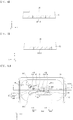
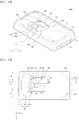
- FIG. 1 illustrates a top perspective view of a light-emitting device package 100A according to an embodiment
- FIG. 2 illustrates a front view of the light-emitting device package 100A illustrated in FIG. 1
- FIG. 3 illustrates a rear view of the light-emitting device package 100A illustrated in FIG. 1
- FIG. 4 illustrates a left side view of the light-emitting device package 100A illustrated in FIG. 1
- FIG. 5 illustrates a right side view of the light-emitting device package 100A illustrated in FIG. 1
- FIG. 6a illustrates a plan view illustrating an embodiment of the light-emitting device package 100A illustrated in FIG. 1
- FIG. 6b illustrates a plan view illustrating another embodiment of the light-emitting device package 100A illustrated in FIG. 1
- FIG. 7 illustrates a bottom view of an embodiment of the light-emitting device package 100A illustrated in FIG. 1
- FIG. 8 illustrates a cross-sectional view taken along line A-A' illustrated in FIG. 6a
- FIG. 9 illustrates a cross-sectional view taken along line B-B' illustrated in FIG. 6a .
- the light-emitting device package 100A illustrated in FIG. 1 may have plan views and cross-sectional views different from the plan views and the cross-sectional views illustrated respectively in FIGs. 6a , 6b , 8 and 9 .
- the light-emitting device package 100A illustrated in FIGs. 6a and 6b may have a perspective view and cross-sectional views different from the perspective view and the cross-sectional views illustrated in FIGs. 1 , 8 and 9
- the light-emitting device package 100A illustrated in FIGs. 8 and 9 may have a perspective view and plan views different from the perspective view and the plan views illustrated in FIGs. 1 , 6a and 6b .
- the light-emitting device package 100A may include two lead frames LF1 and LF2, a package body 110, an insulation layer 114, a light-emitting device 120, first to third wires 132, 134 and 136, a Zener diode (ZD) 140, and a molding member 150.
- ZD Zener diode
- the two lead frames LF1 and LF2 may be disposed so as to be electrically separated from each other.
- the insulation layer 114 may be disposed between the two lead frames LF1 and LF2 so as to electrically insulate the two lead frames LF1 and LF2 from each other.
- the two lead frames LF1 and LF2 may be disposed so as to be spaced apart from each other along the y-axis.
- the insulation layer 114 may include at least one of SiO 2 , TiO 2 , ZrO 2 , Si 3 N 4 , Al 2 O 3 or MgF 2 , but the embodiment is not limited as to the material of the insulation layer 114.
- the insulation layer 114 and the package body 110 may be separate layers, but the embodiment is not limited thereto. That is, when the package body 110 includes an insulation material having an electrical insulation property, the insulation layer 114 and the package body 110 may be integrally formed with each other.
- the light-emitting device 120 may be disposed on any one lead frame among the two lead frames.
- the lead frame on which the light-emitting device 120 is disposed is referred to as a "second lead frame LF2" and the lead frame on which the light-emitting device 120 is not disposed is referred to as a "first lead frame LF1".
- the second lead frame LF2 may include a first device area DA1.
- the first device area DA1 may be defined as an area, in which the light-emitting device 120 may be disposed, of the front surface of the second lead frame LF2, which is not covered by the package body 110 and is exposed. Since the first device area DA1 is an exposed area for allowing the light-emitting device 120 to be disposed thereon, the surface area thereof may be determined by the size of the light-emitting device 120.
- the first lead frame LF1 may include a first lateral portion LF1-S.
- the first lateral portion LF1-S may be shaped so as to protrude from one side surface S1 among multiple side surfaces of the package body 110.
- the second lead frame LF2 may include a second lateral portion LF2-S.
- the second lateral portion LF2-S may be shaped so as to protrude from the side surface S2 opposite the side surface S1 of the package body 110.
- the embodiment is not limited as to the specific shape of the first and second lateral portions LF1-S and LF2-S.
- each of the first lead frame LF1 and the second lead frame LF2 may be exposed from a lower surface S3 of the package body 110.
- Each of the first and second lead frames LF1 and LF2 may be formed using a conductive material such as a metal, for example, one of titanium (Ti), copper (Cu), nickel (Ni), gold (Au), chrome (Cr), tantalum (Ta), platinum (Pt), tin (Sn), silver (Ag), and phosphor (P) or alloys thereof, and may be formed in a single layer or in multiple layers.
- a conductive material such as a metal, for example, one of titanium (Ti), copper (Cu), nickel (Ni), gold (Au), chrome (Cr), tantalum (Ta), platinum (Pt), tin (Sn), silver (Ag), and phosphor (P) or alloys thereof, and may be formed in a single layer or in multiple layers.
- the light-emitting device 120 may be a horizontal bonding-type light-emitting diode, without limitation thereto. That is, the light-emitting device 120 may be a vertical bonding-type light-emitting diode or a flip-chip-bonding-type light-emitting diode.
- the package body 110 may expose a portion of the insulation layer 114.
- a light-emitting device 120C included therein may be a flip-chip-bonding-type light-emitting diode.
- the light-emitting device 120 may be a light-emitting diode that emits, for example, red, green, blue or white light, but the embodiment is not limited thereto.
- the light-emitting device 120 may be an ultraviolet (UV) light-emitting diode that emits ultraviolet light, without limitation thereto.
- UV ultraviolet
- FIG. 10a illustrates a cross-sectional view of an embodiment 120A of the light-emitting device 120 illustrated in each of FIGs. 1 , 6a , 6b , 8 and 9 .
- the light-emitting device 120A may include a substrate 122A, a light-emitting structure 124A, a first electrode 128A, and a second electrode 129A.
- the substrate 122A may be disposed on the first device area DA1 in the exposed front surface of the second lead frame LF2.
- the substrate 122A may be formed of a material that is suitable for the growth of semiconductor materials, for example, a carrier wafer.
- the substrate 122A may be formed of a material having excellent thermal conductivity.
- the substrate 122A may be a material including at least one of sapphire (Al2O3), GaN, SiC, ZnO, Si, GaP, InP, Ga 2 O 3 , or GaAs, but the embodiment is not limited as to the material of the substrate 122A.
- the substrate 122A may have a concave-and-convex pattern (not illustrated) formed in the upper surface thereof.
- a buffer layer (or a transition layer) (not illustrated) may further be disposed between the same 122A and 124A.
- the buffer layer may include at least one material selected from the group consisting of Al, In, N and Ga, without limitation thereto.
- the buffer layer may be formed in a single layer or in multiple layers.
- the light-emitting structure 124A may be disposed on the substrate 122A.
- the light-emitting structure 124A may include a first conductive semiconductor layer 124A-1, an active layer 124A-2, and a second conductive semiconductor layer 124A-3, which are sequentially disposed on the substrate 122A.
- the first conductive semiconductor layer 124A-1 is disposed on the substrate 122A.
- the first conductive semiconductor layer 124A-1 may be formed of, for example, group III-V or group II-VI compound semiconductors and may be doped with a first conductive dopant.
- the first conductive dopant may be an n-type dopant including Si, Ge, Sn, Se or Te, without limitation thereto.
- the first conductive semiconductor layer 124A-1 may include a semiconductor material having a composition equation of Al x In y Ga (1-x-y) N (0 ⁇ x ⁇ 1, 0 ⁇ y ⁇ 1, 0 ⁇ x+y ⁇ 1).
- the first conductive semiconductor layer 124A-1 may include one or more of GaN, InN, AlN, InGaN, AlGaN, InAlGaN, AlInN, AlGaAs, InGaAs, AlInGaAs, GaP, AlGaP, InGaP, AlInGaP, and InP.
- the active layer 124A-2 may be disposed between the first conductive semiconductor layer 124A-1 and the second conductive semiconductor layer 124A-3.
- the active layer 124A-2 is a layer in which electrons (or holes) introduced through the first conductive semiconductor layer 124A-1 and holes (or electrons) introduced through the second conductive semiconductor layer 124A-3 meet each other in order to emit light having energy determined by the intrinsic energy band of a material constituting the active layer 124A-2.
- the active layer 124A-2 may have at least one of a single well structure, a multi-well structure, a single quantum well structure, a multi quantum well (MOW) structure, a quantum wire structure, or a quantum dot structure.
- MOW multi quantum well
- the well layer/barrier layer of the active layer 124A-2 may have one or more paired structure of InGaN/GaN, InGaN/InGaN, GaN/AlGaN, InAlGaN/GaN, GaAs(InGaAs)/AlGaAs, and GaP(InGaP)/AlGaP, without limitation thereto.
- the well layer may be formed of a material having band-gap energy lower than the band-gap energy of the barrier layer.
- a conductive clad layer may be formed on and/or under the active layer 124A-2.
- the conductive clad layer may be formed of semiconductors having band-gap energy higher than the band-gap energy of the barrier layer of the active layer 124A-2.
- the conductive clad layer may include GaN, AlGaN, InAlGaN, or a super-lattice structure.
- the conductive clad layer may be n-type or p-type doped.
- the embodiment is not limited as to the wavelength band of light emitted from the active layer 124A-2.
- the second conductive semiconductor layer 124A-3 may be disposed on the active layer 124A-2.
- the second conductive semiconductor layer 124A-3 may be formed of compound semiconductors, and may be formed of, for example, group III-V or group II-VI compound semiconductors.
- the second conductive semiconductor layer 124A-3 may include a semiconductor material having a composition equation of In x Al y Ga (1-x-y) N (0 ⁇ x ⁇ 1, 0 ⁇ y ⁇ 1, 0 ⁇ x+y ⁇ 1).
- the second conductive semiconductor layer 124A-3 may be doped with a second conductive dopant.
- the second conductive dopant may be a p-type dopant and may include, for example, Mg, Zn, Ca, Sr, or Ba.
- the first conductive semiconductor layer 124A-1 may be formed as an n-type semiconductor layer, and the second conductive semiconductor layer 124A-3 may be formed as a p-type semiconductor layer.
- the first conductive semiconductor layer 124A-1 may be formed as a p-type semiconductor layer, and the second conductive semiconductor layer 124A-3 may be formed as an n-type semiconductor layer.
- the light-emitting structure 124A may be formed to have one of an n-p junction structure, a p-n junction structure, an n-p-n junction structure, and a p-n-p junction structure.
- the first electrode 128A may be disposed on the first conductive semiconductor layer 124A-1, which is exposed by mesa etching. That is, the first conductive semiconductor layer 124A-1 may be exposed by mesa-etching a portion of the second conductive semiconductor layer 124A-3, the active layer 124A-2, and the first conductive semiconductor layer 124A-1.
- the first electrode 128A may include an ohmic contact material so as to perform an ohmic function, it may be not necessary to dispose a separate ohmic layer (not illustrated). Alternatively, a separate ohmic layer may be disposed on or under the first electrode 128A.
- the second electrode 129A may be disposed on the second conductive semiconductor layer 124A-3 and may be electrically connected to the second conductive semiconductor layer 124A-3.
- the second electrode 129A may include a transparent electrode layer (not illustrated).
- the transparent electrode layer may be a transparent conductive oxide (TCO) layer.
- the transparent electrode layer may include at least one of indium tin oxide (ITO), indium zinc oxide (IZO), indium zinc tin oxide (IZTO), indium aluminum zinc oxide (IAZO), indium gallium zinc oxide (IGZO), indium gallium tin oxide (IGTO), aluminum zinc oxide (AZO), antimony tin oxide (ATO), gallium zinc oxide (GZO), IrOx, RuOx, RuOx/ITO, Ni/IrOx/Au, or Ni/IrOx/Au/ITO, without limitation thereto.
- ITO indium tin oxide
- IZO indium zinc oxide
- IZTO indium aluminum zinc oxide
- IGZO indium gallium zinc oxide
- IGTO indium gallium tin oxide
- ATO antimony tin oxide
- GZO gallium zinc oxide
- the second electrode 129A may have ohmic characteristics, and may include a material for ohmic contact with the second conductive semiconductor layer 124A-3. When the second electrode 129A performs an ohmic function, no separate ohmic layer (not illustrated) may be formed.
- Each of the first and second electrodes 128A and 129A may be formed of a material, which may not absorb, but may transmit light emitted from the active layer 124A-2 and which may be grown to have a high quality on the first and second conductive semiconductor layers 124A-1 and 124A-3.
- each of the first and second electrodes 128A and 129A may be formed of a metal, and may be formed of Ag, Ni, Al, Rh, Pd, Ir, Ru, Mg, Zn, Pt, Au, Hf, or selective combinations thereof.
- FIG. 10b illustrates a cross-sectional view of another embodiment 120B of the light-emitting device 120 illustrated in each of FIGs. 1 , 6a , 6b , 8 and 9 .
- the light-emitting device 120B may include a supporting substrate 122B, a reflective layer 126, a light-emitting structure 124B, and a first electrode 128B.
- the supporting substrate 122B supports the light-emitting structure 124B.
- the supporting substrate 122B may be formed of a metal or a semiconductor material.
- the supporting substrate 122B may be formed of a material having high electrical and thermal conductivity.
- the supporting substrate 122B may be a metal material including at least one of copper (Cu), copper (Cu) alloy, gold (Au), nickel (Ni), molybdenum (Mo), or copper-tungsten (Cu-W), or may be semiconductors including at least one of Si, Ge, GaAs, ZnO, or SiC.
- the reflective layer 126 may be disposed on the supporting substrate 122B.
- the supporting substrate 122B may perform a role corresponding to that of the second electrode 129A illustrated in FIG. 10a .
- the reflective layer 126 serves to reflect light, which is emitted from the active layer 124B-2 of the light-emitting structure 124B and is directed to the supporting substrate 122B, rather than being emitted upward. That is, the reflective layer 126 may reflect light introduced from the light-emitting structure 124B, thereby increasing the light extraction efficiency of the light-emitting device 120B.
- the reflective layer 126 may be formed of a light reflection material, for example, a metal or an alloy including at least one or Ag, Ni, Al, Rh, Pd, Ir, Ru, Mg, Zn, Pt, Au or Hf, but the embodiment is not limited thereto.
- the reflective layer 126 may be formed in multiple layers using a light-transmitting conductive material such as a metal or alloy, or IZO, IZTO, IAZO, IGZO, IGTO, AZO, or ATO, and for example, may be formed of IZO/Ni, AZO/Ag, IZO/Ag/Ni, or AZO/Ag/Ni.
- a light-transmitting conductive material such as a metal or alloy, or IZO, IZTO, IAZO, IGZO, IGTO, AZO, or ATO, and for example, may be formed of IZO/Ni, AZO/Ag, IZO/Ag/Ni, or AZO/Ag/Ni.
- an ohmic layer (not illustrated) may be disposed between the reflective layer 126 and the second conductive semiconductor layer 124B-3.
- the ohmic layer may be in ohmic contact with the second conductive semiconductor layer 124B-3, thereby serving to assist the smooth supply of power to the light-emitting structure 124B.
- the light-emitting device 120B is illustrated as including the reflective layer 126, but the embodiment is not limited thereto. That is, the reflective layer 126 may be omitted in some cases.
- the light-emitting structure 124B may be disposed on the reflective layer 126.
- the light-emitting structure 124B may include a second conductive semiconductor layer 124B-3, an active layer 124B-2, and a first conductive semiconductor layer 124B-1, which are sequentially disposed on the reflective layer 126.
- the first conductive semiconductor layer 124B-1, the active layer 124B-2, and the second conductive semiconductor layer 124B-3 illustrated in FIG. 10b may perform the same functions as those of each of the first conductive semiconductor layer 124A-1, the active layer 124A-2, and the second conductive semiconductor layer 124A-3 illustrated in FIG. 10a , and thus a repeated description thereof will be omitted.
- the first electrode 128B may be disposed on the first conductive semiconductor layer 124A-1 of the light-emitting structure 124B.
- the first electrode 128B may perform a role corresponding to that of the first electrode 128A illustrated in FIG. 10a .
- the first electrode 128B may have a predetermined pattern shape.
- the upper surface of the first conductive semiconductor layer 124B-1 may be provided with a pattern (not illustrated) having roughness in order to increase light extraction efficiency.
- the upper surface of the first electrode 128B may be also provided with a pattern (not illustrated) having roughness.
- the light-emitting device 120 illustrated in each of FIGs. 1 , 6a , 6b , 8 and 9 may have the structure illustrated in FIG. 10a or FIG. 10b as described above, but the embodiments are not limited thereto. That is, it is to be noted that the light-emitting device 120 included in the light-emitting device package 100A of the embodiment may have a structure different from the structure illustrated in FIG. 10a or FIG. 10b .
- the first electrodes 128A and 128B of the light-emitting devices 120, 120A and 120B illustrated respectively in FIGs. 1 , 6a , 6b , 8, 9, 10a and 10b may be electrically connected to the first lead frame LF1
- the second electrodes 129A and 129B may be electrically connected to the second lead frame LF2.
- FIG. 11 illustrates an enlarged cross-sectional view of an embodiment K1 of portion "K" illustrated in FIG. 8 .
- the package body 110 may cover a first boundary 114-1 between the first lead frame LF1 and the insulation layer 114 and a second boundary 114-2 between the second lead frame LF2 and the insulation layer 114. At this time, as illustrated in FIG. 8 , the package body 110 may cover only a region up to the second boundary 114-2, and as illustrated in FIG. 11 , the package body 110 may cover a region up to a zero point P0 of the second lead frame LF2 beyond the second boundary 114-2.
- first electrodes 128A and 128B and the second electrodes 129A and 122B of the light-emitting devices 120, 120A and 120B may be electrically connected to the first and second lead frames LF1 and LF2 via wires, but the embodiments are not limited thereto.
- the first wire 132 serves to electrically connect the first electrodes 128A and 128B of the light-emitting devices 120, 120A and 120B to the first lead frame LF1.
- one end of the first wire 132 may be electrically connected to the first electrodes 128A and 128B of the light-emitting devices 120, 120A and 120B, and the other end thereof may be electrically connected to the first lead frame LF1.
- the front surface of the first lead frame LF1 may include a second bonding area BA2.
- the second bonding area BA2 may be an area that is electrically connected to the other end of the first wire 132 on the front surface of the first lead frame LF1, which is not covered by the package body 110 and is exposed.
- the second bonding area BA2 may be exposed through a first blind hole TH1 illustrated in FIG. 6a (or a third blind hole TH3 illustrated in FIG. 6b ), which is included in the package body 110. Since the second bonding area BA2 is an area for the bonding of the first wire 132, the second bonding area BA2 may have a surface area greater than the minimum surface area required for wire bonding.
- first blind hole TH1 (or the third blind hole TH3) may be spaced apart from the first device area DA1, as illustrated in FIGs. 1 , 6a and 6b , but the embodiment is not limited thereto.
- the second wire 134 serves to electrically connect the second electrode 129A of the light-emitting devices 120 and 120A to the second lead frame LF2.
- one end of the second wire 134 may be electrically connected to the second electrode 129A of the light-emitting devices 120 and 120A, and the other end thereof may be electrically connected to the second lead frame LF2.
- the front surface of the second lead frame LF2, which is exposed rather than being covered by the package body 110 may include a first bonding area BA1.
- the first bonding area BA1 may include an area, which is electrically connected to the other end of the second wire 134, of the front surface of the second lead frame LF2.
- the first bonding area BA1 may be exposed through a first groove H1, which is included in the package body 110.
- the first bonding area BA1 may be disposed close to the first device area DA1, but the embodiment is not limited thereto. That is, the first bonding area BA1 may be disposed so as to extend from the first device area DA1.
- the light-emitting device package 100A may not include the second wire 134.
- the supporting substrate 122B which serves as the second electrode in the light-emitting device 120B, may be directly electrically connected to the second lead frame LF2 without a wire.
- the Zener diode 140 may be disposed on the first lead frame LF1 in order to increase the voltage that can be withstood by the light-emitting device package 100A.
- the third wire 136 serves to electrically connect the Zener diode 140 and the second lead frame LF2 to each other. To this end, one end of the third wire 136 may be electrically connected to the Zener diode 140 and the other end thereof may be electrically connected to the second lead frame LF2.
- the front surface of the second lead frame LF2 may include a third bonding area BA3.
- the third bonding area BA3 may include an area, which is electrically connected to the other end of the third wire 136, of the front surface of the second lead frame LF2.
- the third bonding area BA3 may be exposed through a third groove H3, which is included in the package body 110.
- the third bonding area BA3 may be disposed close to the first device area DA1, but the embodiment is not limited thereto. That is, the third bonding area BA3 may be disposed so as to extend from the first device area DA1.
- first and third grooves H1 and H3 described above may be recessed in an inclined surface 112 of the package body 110 on the second lead frame LF2.
- first groove H1 may be recessed along the y-axis in the inclined surface 112 on the boundary between the first device area DA1 and the first bonding area BA1 of the second lead frame LF2.
- third groove H3 may be recessed along the -x-axis in the inclined surface 112 on the boundary between the first device area DA1 and the third bonding area BA3 of the second lead frame LF2.
- Each of the first and third bonding areas BA1 and BA3 described above are areas for the bonding of the second and third wires 134 and 136, and therefore may have a surface area greater than the minimum surface area required for wire bonding.
- An example of the respective sizes of the first and third bonding areas BA1 and BA3 will be described later.
- the front surface of the first lead frame LF1 may further include a second device area DA2.
- the second device area DA2 may be defined as an area, which is allotted to dispose the Zener diode 140, of the front surface of the first lead frame LF1.
- the second device area DA2 is exposed in order to dispose the Zener diode 140 thereon, and therefore, the surface area thereof may be determined by the size of the Zener diode 140.
- An example of the size of the second device area DA2 will be described later.
- the second bonding area BA2 and the second device area DA2 may be disposed on the front surface of the first lead frame LF1 so as to be spaced apart from each other as illustrated in FIG. 6a , or so as to be in contact with and be connected to each other as illustrated in FIG. 6b .
- the light-emitting device package illustrated in FIG. 6b is the same as the light-emitting device package illustrated in FIG. 6a , and thus a description of the same parts will be omitted and only differences therebetween will be described.
- the package body 110 may further include a second blind hole TH2.
- the second blind hole TH2 may serve to expose a portion to which one end of the third wire 136 is to be connected.
- the second device area DA2 may be exposed through the second blind hole TH2.
- the second device area DA2 may be exposed through the third blind hole TH3.
- the Zener diode 140 may be exposed through the second blind hole TH2 (or the third blind hole TH3).
- the first and second blind holes TH1 and TH2 are separately formed so as to be spaced apart from each other.
- the package body 110 illustrated in FIG. 6b has therein the third blind hole TH3, which is acquired by integrally interconnecting the first and second blind holes TH1 and TH2 illustrated in FIG. 6a .
- the second blind hole TH2 (or the third blind hole TH3) may not expose the entire second device area DA2, but may expose only a portion of the Zener diode 140 to which one end of the third wire 136 is connected.
- the second blind hole TH2 (or the third blind hole TH3) may be located so as to be spaced apart from the first device area DA1, as illustrated in FIGs. 1 , 6a and 6b , but the embodiment is not limited thereto.
- the first blind hole TH1 may be spaced apart from the first device area DA1 by a first predetermined distance D1
- the second blind hole TH2 may be spaced apart from the first device area DA1 by a second predetermined distance D2.
- the third blind hole TH3 may be spaced apart from the first device area DA1 by the second predetermined distance D2 (or the first predetermined distance D1).
- a first minimum distance which is the minimum value of the first predetermined distance D1
- a second minimum distance which is the minimum value of the second predetermined distance D2
- the first predetermined distance D1 when the first predetermined distance D1 is smaller than 50 ⁇ m, it may be difficult to form the first blind hole TH1.
- the first predetermined distance D1 when the first blind hole TH1 is formed through an injection process, it may be difficult to perform the injection process when the first predetermined distance D1 is smaller than 50 ⁇ m. Therefore, the first predetermined distance D1 may be 50 ⁇ m or more, but the embodiment is not limited thereto.
- the second predetermined distance D2 when the second predetermined distance D2 is smaller than 50 ⁇ m, it may be difficult to form the second blind hole TH2.
- the second predetermined distance D2 when the second blind hole TH2 is formed through an injection process, it may be difficult to perform the injection process when the second predetermined distance D2 is smaller than 50 ⁇ m. Therefore, the second predetermined distance D2 may be 50 ⁇ m or more, but the embodiment is not limited thereto.
- the second predetermined distance D2 when the second predetermined distance D2 (or the first predetermined distance D1) is smaller than 50 ⁇ m, it may be difficult to form the third blind hole TH3.
- the third blind hole TH3 when the third blind hole TH3 is formed through an injection process, it may be difficult to perform the injection process when the second predetermined distance D2 (or the first predetermined distance D1) is smaller than 50 ⁇ m. Therefore, the second predetermined distance D2 (or the first predetermined distance D1) may be 50 ⁇ m or more, but the embodiment is not limited thereto.
- FIG. 12 illustrates a cross-sectional view taken along line C-C' illustrated in FIGs. 6a and 6b
- FIG. 13 illustrates a cross-sectional view taken along line D-D' illustrated in FIGs. 6a and 6b .
- light emitted from the light-emitting device of the light-emitting device package may be absorbed by the Zener diode, which may reduce the total quantity of light emitted by the light-emitting device package.
- a first thickness t1 of the package body 110 disposed between the Zener diode 140 and the light-emitting device 120 may be greater than the thickness T1 of the light-emitting device 120 or the thickness T2 of the Zener diode 140.
- the Zener diode 140 since the Zener diode 140 is hidden by the package body 110, the light emitted from the light-emitting device 120 is not absorbed by the Zener diode 140, which may increase the light extraction efficiency of the light-emitting device package 100A.
- the first thickness t1 may be greater than the thickness T2 of the Zener diode 140.
- the first thickness t1 may be greater than 50 ⁇ m.
- the bottom surface of the cavity C which has reflectance lower than that of the inclined surface 112, may be excessively exposed, which may deteriorate the light extraction efficiency thereof.
- the first thickness t1 may be greater than 50 ⁇ m and equal to or less than 200 ⁇ m, but the embodiment is not limited thereto.
- the first blind hole TH1 may have a shape suitable for allowing the first wire 132 to be connected to the second bonding area BA2
- the second blind hole TH2 may have a shape suitable for allowing the third wire 136 to be connected to the Zener diode 140
- the third blind hole TH3 may have a shape suitable for allowing the first wire 132 to be connected to the second bonding area BA2 and allowing the third wire 136 to be connected to the Zener diode 140.
- the second blind hole TH2 (or the third blind hole TH3) may be vertically formed in a direction that is parallel to the thickness direction (e.g.
- the first blind hole TH1 may be vertically formed in the direction that is parallel to the thickness direction of the first lead frame LF1, or may be formed to be inclined by the first inclination angle ⁇ 1, in the same manner as the second blind hole TH2.
- the first and third wires 132 and 136 may be more easily introduced into the first to third blind holes TH1, TH2 and TH3.
- the package body 110 may cover the entire insulation layer 114, but the embodiment is not limited thereto.
- the package body 110 may cover only a portion of the insulation layer 114.
- the package body 110 may cover at least a portion of the insulation layer 114.
- FIG. 14 illustrates a top perspective view of the light-emitting device package 100B according to another embodiment
- FIG. 15 illustrates a plan view of the light-emitting device package 100B illustrated in FIG. 14 .
- the light-emitting device package 100B illustrated in FIGs. 14 and 15 is substantially the same as the light-emitting device package 100A illustrated in FIGs. 1 and 6a , and thus a description related to the same parts will be omitted and only differences therebetween will be described below.
- the front view, the rear view, the left side view, the right side view, and the bottom view of the light-emitting device package 100B are respectively the same as the front view of FIG. 2 , the rear view of FIG. 3 , the left side view of FIG. 4 , the right side view of FIG. 5 , and the bottom view of FIG. 7 , and thus a repeated description thereof will be omitted.
- the package body 110 may include the second groove H2, which exposes the second bonding area BA2 of the first lead frame FL1. That is, the second bonding area BA2 may be exposed through the first blind hole TH1, as illustrated in FIGs. 1 and 6a , may be exposed through the third blind hole TH3, as illustrated in FIG. 6b , or may be exposed through the second groove H2, as illustrated in FIGs. 14 and 15 .
- the embodiments are not limited thereto. That is, according to another embodiment, it is to be noted that, even when a portion of the insulation layer 114 is exposed as illustrated in FIGs. 14 and 15 , the second bonding area BA2 may be exposed through the first blind hole TH1, as illustrated in FIGs. 1 and 6a (or the third blind hole TH3 illustrated in FIG. 6b ).
- the second groove H2 may be recessed in the inclined surface 112 of the package body 110 on the first lead frame LF1.
- the second groove H2 may be recessed along the -y-axis in the inclined surface 112 in order to expose the second bonding area BA2 of the first lead frame LF1.
- the above-described second bonding area BA2 is an area for the bonding of the first wire 132, and therefore may have a surface area greater than the minimum surface area required for wire bonding. An example of the size of the second bonding area BA2 will be described later.
- FIG. 16 illustrates a top perspective view of the light-emitting device package 100C according to still another embodiment
- FIG. 17 illustrates a plan view of the light-emitting device package 100C illustrated in FIG. 16
- FIG. 18 illustrates a cross-sectional view taken along line E-E' illustrated in FIG. 17 .
- the light-emitting device package 100C illustrated in FIGs. 16 and 17 is substantially the same as the light-emitting device 100B illustrated in FIGs. 14 and 15 , and thus a description related to the same parts will be omitted, and only differences therebetween will be described below.
- the front view, the rear view, the left side view, the right side view, and the bottom view of the light-emitting device package 100C are respectively the same as the front view of FIG. 2 , the rear view of FIG. 3 , the left side view of FIG. 4 , the right side view of FIG. 5 , and the bottom view of FIG. 7 , and thus a repeated description thereof will be omitted.
- FIG. 19 illustrates an enlarged cross-sectional view of an embodiment M1 of portion "M” illustrated in FIG. 18, and FIG. 20 illustrates an enlarged cross-sectional view of another embodiment M2 of portion "M” illustrated in FIG. 18 .
- the light-emitting devices 120, 120A and 120B may have a horizontal bonding-type structure, as illustrated in FIG. 10a , or may have a vertical bonding-type structure, as illustrated in FIG. 10b .
- the light-emitting device 120C may have a flip-chip-bonding-type structure, as illustrated in FIGs. 17 to 20 .
- the light-emitting device 120C having a flip-chip-bonding-type structure may include a substrate 122C, a light-emitting structure 124C, and first and second electrodes 128C and 129C.
- the substrate 122C, the light-emitting structure 124C, and the first and second electrodes 128C and 129C perform the same roles as the substrate 122A, the light-emitting structure 124A, and the first and second electrodes 128A and 129A illustrated in FIG. 10a , respectively, and thus a repeated description thereof will be omitted.
- first conductive semiconductor layer 124C-1, the active layer 124C-2, and the second conductive semiconductor layer 124C-3 perform the same roles as the first conductive semiconductor layer 124A-1, the active layer 124A-2, and the second conductive semiconductor layer 124A-3 illustrated in FIG. 10a respectively.
- the light-emitting device 100C illustrated in FIGs. 19 and 20 has a flip-chip-bonding-type structure
- the light emitted from the active layer 124C-2 may be emitted through the first electrode 128C, the first conductive semiconductor layer 124C-1, and the substrate 122C.
- the first electrode 128C, the first conductive semiconductor layer 124C-1, and the substrate 122C may be formed of materials that transmit light.
- the second conductive semiconductor layer 124C-3 and the second electrode 129C may be formed of materials that transmit light or do not transmit light, or materials that reflect light, but the embodiment is not limited to specific materials.
- each of the first and second electrodes 128C and 129C may be formed of materials that may not absorb the light emitted from the active layer 124C-2, but that may reflect or transmit the light, and that may be grown so as to have a high quality on the first and second conductive semiconductor layers 124C-1 and 124C-3.
- each of the first and second electrodes 128C and 129C may be formed of a metal, and may be formed of Ag, Ni, Al, Rh, Pd, Ir, Ru, Mg, Zn, Pt, Au, Hf, or selective combinations thereof.
- the light-emitting device package 100C may further include first and second solder portions 162 and 164.
- the first solder portion 162 may be disposed between the first electrode 128C of the light-emitting device 120C and the first lead frame LF1, and may electrically connect the first electrode 128C and the first lead frame LF1 to each other.
- the first lead frame LF1, on which the first solder portion 162 is disposed may be close to the remaining portion of the insulation layer 114, which is not covered by the package body 110 and is exposed.
- the second solder portion 164 may be disposed between the second electrode 129C of the light-emitting device 120C and the second lead frame LF2, and may electrically connect the second electrode 129C and the second lead frame LF2 to each other.
- the second lead frame LF2, on which the second solder portion 164 is disposed may be close to the remaining portion of the insulation layer, which is not covered by the package body 110 and is exposed.
- Each of the first solder portion 162 and the second solder portion 164 may be solder paste or a solder ball.
- the light-emitting device 120C illustrated in FIGs. 19 and 20 are merely given by way of example, and the embodiment is not limited thereto. That is, the light-emitting device package 100C may include various other shapes of light-emitting devices having a flip-chip-bonding-type structure, unlike that illustrated in FIGs. 19 and 20 .
- each of the first and second device areas DA1 and DA2 may have a polygonal, circular or oval planar shape depending on the purposes and designs thereof, but the embodiment is not limited as to the shape of the first and second device areas DA1 and DA2.
- each of the first and second device areas DA1 and DA2 may have a rectangular planar shape having rounded corners.
- the inclined surface 112 of the package body 110 may define a cavity C together with the exposed front surface of at least one of the first or second lead frame LF1 or LF2, and may reflect the light emitted from the light-emitting devices 120, 120A, 120B and 120C. That is, the inclined surface 112 of the package body 110 may define the cavity C together with the front surface of at least one of the first or second lead frame LF1 or LF2, which is not covered by the package body 110 and is exposed.
- the inclined surface 112 may be disposed on the periphery of the light-emitting devices 120, 120A, 120B and 120C.
- the light-emitting devices 120, 120A and 120B may be disposed in the first device area DA1 of the exposed front surface of the second lead frame LF2 inside the cavity C, and the light-emitting device 120C may be disposed over the exposed front surfaces of the first and second lead frames LF1 and LF2, which is exposed inside the cavity C.
- the shape of the cavity C viewed from the top may be a circular, polygonal, oval, cup, or concave container shape
- the inclined surface 112 of the package body 110 may be orthogonal to or inclined relative to at least one exposed front surface (or exposed top surface) of the first or second lead frame LF1 or LF2.
- the second angle ⁇ 2 between the inclined surface 112 and the top surface of the second lead frame LF2 may be an acute angle. That is, the second angle ⁇ 2 may be greater than 0° and smaller than 90°, and may be, for example, 30° or less, but the embodiment is not limited thereto.
- the width W of the cavity C may be increased with increasing distance from the bottom surface of the cavity C (i.e. in the +z-axis). That is, the width W of the cavity C may be the smallest at the bottom surface of the cavity C on which the light-emitting device 120 is disposed and may be the greatest at the top surface of the package body 110.
- the inclined surface 112 may reflect the light emitted from the light-emitting devices 120, 120A, 120B and 120C.
- the reflectance of the inclined surface 112 may be greater than the reflectance of the exposed front surface of at least one of the first or second lead frame LF1 or LF2.
- at least one of the first or second lead frame LF1 or LF2, which is not covered by the package body 110 and is exposed, may be formed of a reflective material, for example, silver (Ag), in order to reflect the light emitted from the light-emitting device 120, and the inclined surface 112 may be formed of a resin material such as polyphthalamide (PPA) having reflectance higher than that of the first or second lead frame LF1 or LF2.
- PPA polyphthalamide
- the inclined surface 112 of the package body 110 may have a concave shape, a convex shape, or a stepped shape toward the cavity C.
- the inclined surface 112 may have a convex shape toward the cavity C, as illustrated in FIG. 18 , may have a stepped shape toward the cavity C, as illustrated in FIG. 19 , or may have a concave shape toward the cavity C, as illustrated in FIG. 20 .
- the package body 110 may further include a stepped portion 118.
- the stepped portion 118 may be disposed between the lower end 112-1 of the inclined surface 112 and the bottom surface of the cavity C (e.g. the top surface of the first lead frame LF1).
- the stepped portion 118 illustrated in FIG. 20 may also be disposed in the light-emitting device package 100A or 100B according to one embodiment or another embodiment.
- the stepped portion 118 illustrated in FIG. 20 may also be disposed between the lower end of the inclined surface 112 and the top surface of the second lead frame LF2.
- a first height h1 from the bottom surface of the cavity C, i.e. the top surface of the first or second lead frame LF1 or LF2, which is not covered by the package body 110 and is exposed, to the top surface of the stepped portion 118 may be smaller than a second height h2 from the bottom surface of the cavity C to the active layer 124C-2.
- the first height h1 of the stepped portion 118, illustrated in FIG. 20 may be 50 ⁇ m
- the second height h2 from the bottom surface of the cavity C to the active layer 124A-2 or 124B-2 illustrated in FIG. 10a or 10b may range from 100 ⁇ m to 150 ⁇ m, but the embodiment is not limited thereto.
- the package body 110 may be formed as a silicon-based wafer level package, a silicon substrate, or a silicon carbide (SiC) substrate or aluminum nitride (AlN) substrate having high insulation or thermal conductivity, may be formed of a resin material such as polyphthalamide (PPA) having high reflectance, or may be formed of epoxy molding compound (EMC), but the embodiment is not limited as to the material of the package body 110.
- PPA polyphthalamide
- EMC epoxy molding compound
- the light-emitting device packages 100A, 100B and 100C may achieve increased light extraction efficiency as the distance between the inclined surface 112 and the light-emitting devices 120, 120A, 120B and 120C in the width direction is reduced. This is because the smaller the distance, the smaller the area of the bottom surface of the cavity C and the greater the area of the inclined surface 112, and because the reflectance of the inclined surface 112 is greater than the reflectance of the bottom surface of the cavity C as described above.
- the width direction may be a direction that crosses the thickness direction of the light-emitting devices 120, 120A, 120B and 120C, and may be, for example, a direction that is orthogonal to the thickness direction of the light-emitting devices 120, 120A, 120B and 120C.
- the lower end of the inclined surface 112 that corresponds to the side surface of the cavity C and the light-emitting devices 120, 120A, 120B and 120C disposed on the bottom surface of the cavity C may be spaced apart from each other by a predetermined distance.
- the predetermined distance may be at least one of the distance D3 along the y-axis or the distance D4 along the x-axis illustrated in FIGs. 6a , 6b , 8 , 15 , and 17 to 20 .
- the first device area DA1 may have the processing defects, for example, the first device area DA1 may not be formed to have a desired surface area.
- each of the distances D3 and D4 may be 30 ⁇ m or more. As described above, when each of the distances D3 and D4 is smaller, the surface area of the inclined surface 112 may be greater than the surface area of the bottom surface of the cavity C, which may increase light extraction efficiency. Therefore, each of the distances D3 and D4 may be 30 ⁇ m, but the embodiment is not limited thereto.
- the length of the first bonding area BA1 along each of the x-axis and the y-axis when the length of the first bonding area BA1 along each of the x-axis and the y-axis is zero, the other end of the second wire 134 may not have a sufficient surface area for the bonding of the second lead frame LF2.
- the length of the first bonding area BA1 along each of the x-axis and the y-axis is greater than 400 ⁇ m, the bottom surface of the cavity C, which has reflectance lower than that of the inclined surface 112, may be excessively exposed, which may deteriorate light extraction efficiency.
- the length of the first bonding area BA1 along each of the x-axis and the y-axis may be greater than 0 ⁇ m and equal to or greater than 400 ⁇ m, but the embodiment is not limited thereto.
- the length of the third bonding area BA3 along each of the x-axis and the y-axis may not have a sufficient surface area for being bonded with the second lead frame LF2.
- the length of the third bonding area BA3 along each of the x-axis and the y-axis is greater than 400 ⁇ m, the bottom surface of the cavity C, which has reflectance lower than that of the inclined surface 112, may be excessively exposed, which may deteriorate light extraction efficiency.
- the length of the third bonding area BA3 along each of the x-axis and the y-axis may be greater than 0 ⁇ m and equal to or greater than 400 ⁇ m, but the embodiment is not limited thereto.
- the surface area of the portion of the front surface of the second lead frame LF2 in which the light-emitting device 120 is disposed may be reduced.
- the length of the first device area DA1 along each of the x-axis and the y-axis may range from 150 ⁇ m to 1050 ⁇ m, but the embodiment is not limited thereto.
- the minimum value of the length of the second device area DA2 along each of the x-axis and the y-axis is determined depending on the size of the Zener diode 140.
- the length of the second device area DA2 along each of the x-axis and the y-axis is greater than 400 ⁇ m, the bottom surface of the cavity C, which has reflectance lower than that of the inclined surface 112, may be excessively exposed, which may deteriorate light extraction efficiency.
- the maximum value of the length of the second device area DA2 along each of the x-axis and the y-axis may be 400 ⁇ m, but the embodiment is not limited thereto.
- FIG. 21 illustrates an enlarged cross-sectional view of a comparative example K2 of portion "K" illustrated in FIG. 8 .
- the package body 110 covers the entire front surface of the first lead frame LF1 and covers the entire front surface of the insulation layer 114 while exposing the first to third blind holes TH1, TH2 and TH3.
- the package body 110 covers the first lead frame LF1 and the insulation layer 114. At this time, the package body 110 may cover a region up to the zero point PO of the top surface LFT2 of the second lead frame LF2. In contrast, referring to FIG. 21 , the package body 110 covers only a region up to the first point P1 on the top surface of the first lead frame LF1 while exposing a portion of the insulation layer 114 and the first lead frame LF1.
- the third angle ⁇ 3 between the inclined surface 112 and the top surface of the second lead frame LF2 illustrated in FIG. 11 is smaller than the fourth angle ⁇ 4 between the inclined surface 112 and the top surface of the first lead frame LF1 illustrated in FIG. 21 .
- the surface area of the inclined surface 112 illustrated in FIG. 11 is greater than the surface area of the inclined surface 112 illustrated in FIG. 21 .
- the third angle ⁇ 3 may be greater than 0° and smaller than 90°.
- the fifth angle ⁇ 5 between the inclined surface 112 and the top surface of the second lead frame LF2 illustrated in FIG. 13 is smaller than the fourth angle ⁇ 4 between the inclined surface 112 and the top surface of the first lead frame LF1 illustrated in FIG. 21 .
- the fifth angle ⁇ 5 may be greater than 0° and smaller than 90°.
- the third angle ⁇ 3 between the inclined surface 112 and the top surface of the second lead frame LF2 along the major axis (e.g. the y-axis) illustrated in FIG. 11 may be smaller than the fifth angle ⁇ 5 between the inclined surface 112 and the top surface of the second lead frame LF2 along the minor axis (e.g. the x-axis) illustrated in FIG. 13 .
- the third angle ⁇ 3 may be 30° and the fifth angle ⁇ 5 may be 45°, but the embodiment is not limited thereto.
- the surface area of the inclined surface 112 increases.
- the reflectance of the inclined surface 112 is greater than the reflectance of each of the first and second lead frames LF1 and LF2.
- outside air such as moisture may permeate into the cavity C of the light-emitting device package from the outside in the arrow direction PH2 through the second boundary 114-2 between the insulation layer 114 and the second lead frame LF2. Due thereto, the reliability of the light-emitting device package may be reduced.
- the length of the path, along which outside air is introduced from the outside into the cavity C of the light-emitting device package 100A in the arrow direction PH1 through the second boundary 114-2, may be increased, and the introduction path becomes more crooked. That is, compared to the light-emitting device package illustrated in FIG. 21 , the light-emitting device package 100A illustrated in FIG. 11 may further increase the length of the introduction path PH1 of the outside air into the cavity C and may cause the introduction path PH1 to be more crooked, which makes it difficult for the outside air to permeate. Therefore, the reliability of the light-emitting device package 100A illustrated in FIG. 11 may be improved relative to the light-emitting device package illustrated in FIG. 21 .
- the package body 110 is disposed so as to expose a portion of the first lead frame LF1 and to expose the entire insulation layer 114. Therefore, when the thicknesses of the first and second lead frames LF1 and LF2 are not secured to some extent, the first and second lead frames LF1 and LF2 may not be sufficiently rigid. To prevent this, for example, the thicknesses of the first and second lead frames LF1 and LF2 need to be greater than 250 ⁇ m.
- the package body 110 is disposed so as to cover the entire front surface of the first lead frame LF1, excluding the portion exposed through the first and second blind holes TH1 and TH2 (or the third blind hole TH3), to cover the entire front surface of the insulation layer 114, and to cover a portion of the front surface of the second lead frame LF2.
- the package body 110 may supplement the rigidity of the first and second lead frames LF1 and LF2, whereby the thicknesses of the first and second lead frames LF1 and LF2 may be reduced.
- the structural rigidity of the light-emitting device package 100A may be increased.
- the rigidity of the first and second lead frames LF1 and LF2 may be secured.
- the minimum value of the sum of the second, third or fourth thickness t2, t3 or t4 and the fifth thickness t5 of the package body 110, which is disposed on the insulation layer 114 and the first lead frame LF1 may be 250 ⁇ m, but the embodiment is not limited thereto.
- second, third and fourth thicknesses t2, t3 and t4 may be the same as or different from each other.
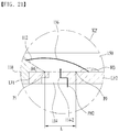
- first planar area planar area of the insulation layer 114 that is covered by the package body 110
- second planar area planar area of the insulation layer 114 that is not covered by the package body 110 and is exposed
- the first planar area of the portion of the insulation layer 114 that is covered by the package body 110 may be represented by the following Equation 1
- the second planar area of the remaining portion of the insulation layer 114 that is exposed through the package body 110 may be represented by the following Equation 2.
- Equation 1 TA 1 x 11 + x 12 ⁇ ⁇ y Equation 2
- TA 2 x 2 ⁇ ⁇ y
- TA1 and TA2 designate the first and second planar areas, respectively, x11 designates the length of an upper end portion of the insulation layer 114 that is covered by the package body 110 along the x-axis, x12 designates the length of a lower end portion of the insulation layer 114 that is covered by the package body 110 along the x-axis, x2 designates the length of a portion of the insulation layer 114 that is not covered by the package body 110 and is exposed along the x-axis, and ⁇ y designates the length of the insulation layer 114 along the y-axis.
- x2 is "0".
- the package body 110 is illustrated as exposing a middle portion of the insulation layer 114.
- the distance x11 or x12 from the tip end of the exposed insulation layer 114 to the edge of the cavity C may be greater than "0", but the embodiment is not limited thereto. According to another embodiment, x11 or x12 may be "0".
- the package body 110 may cover the entire insulation layer 114, as in the light-emitting device package 100A according to the embodiment, or may cover only a portion of the insulation layer 114, as in the light-emitting device packages 100B and 100C according to the other embodiments.
- the first planar area TA1 may be equal to or greater than the second planar area TA2, but the embodiment is not limited thereto.
- the second planar area becomes "0". Therefore, even in the case of the light-emitting device package 100A according to the embodiment, it can be appreciated that the first planar area is greater than the second planar area.
- the surface area of the inclined surface 112 which has reflectance greater than the reflectance of the bottom surface of the cavity C, increases, light extraction efficiency may be increased and the rigidity of the lead frames LF1 and LF2 may be increased.
- the top surface LFT1 of the first lead frame LF1, the top surface LFT2 of the second lead frame LF2, and the top surface 114T of the insulation layer 114 may not be stepped, but may be disposed in the same plane, but the embodiment is not limited thereto. That is, according to another embodiment, the top surface LFT1 of the first lead frame LF1, the top surface LFT2 of the second lead frame LF2, and the top surface 114T of the insulation layer 114 may be stepped, unlike the illustration.
- the illustration of the molding member 150 is omitted in FIGs. 1 , 6a , 6b , 9 , and 14 to 17 .
- the light-emitting device packages 100A, 100B and 100C according to the embodiments may further include the molding member 150.
- the molding member 150 may surround and protect the light-emitting devices 120, 120A, 120B, and 120C.
- the molding member 150 may be formed of, for example, a transparent polymer resin such as silicon (Si), and may include phosphors, and therefore may change the wavelength of the light emitted from the light-emitting devices 120, 120A, 120B and 120C.
- the phosphors may include a fluorescent substance, which serves as a wavelength change material capable of changing light emitted from the light-emitting devices 120, 120A, 120B and 120C into white light, for example, any one of YAG-based, TAG-based, silicate-based, sulfide-based, or nitride-based fluorescent substances, but the embodiment is not limited as to the kind of phosphors.
- the YGA-based and TAG-based fluorescent substances may be selected and used from among (Y, Tb, Lu, Sc, La, Gd, Sm)3(Al, Ga, In, Si, Fe)5(O, S)12:Ce, and the silicate-based fluorescent substance may be selected and used from among (Sr, Ba, Ca, Mg)2SiO4: (Eu, F, Cl).
- the sulfide-based fluorescent substance may be selected and used from among (Ca, Sr)S:Eu, (Sr, Ca, Ba)(Al, Ga)2S4: Eu, and the nitride-based phosphors are at least one material of (Sr, Ca, Si, Al, 0)N:Eu (e.g.
- Red phosphors may include nitride-based phosphors including N(e.g. CaAlSiN3:Eu). Such nitride-based red phosphors may have higher reliability to withstand external environments such as heat and moisture and lower discoloration possibility than sulfide-based phosphors.
- the light-emitting device packages 100A, 100B and 100C may further include a lens (not illustrated) disposed on the molding member 150.
- the lens (not illustrated) may adjust the distribution of light emitted from the light-emitting device packages 100A, 100B and 100C.
- a plurality of light-emitting device packages according to the embodiments may be disposed on a substrate to form an array, and optical members, such as a light guide plate, a prism sheet, and a diffusion sheet may be disposed on the optical path of the light-emitting device packages.
- optical members such as a light guide plate, a prism sheet, and a diffusion sheet may be disposed on the optical path of the light-emitting device packages.
- the light-emitting device packages, the substrate, and the optical members may function as a backlight unit.
- a display apparatus an indicator apparatus, and a lighting apparatus including the light-emitting device packages according to the embodiments may be realized.
- the display apparatus may include a bottom cover, a reflector disposed on the bottom cover, a light-emitting module configured to emit light, a light guide plate disposed in front of the reflector to forwardly guide the light emitted from the light-emitting module, optical sheets including prism sheets disposed in front of the light guide plate, a display panel disposed in front of the optical sheets, an image signal output circuit connected to the display panel so as to supply an image signal to the display panel, and a color filter disposed in front of the display panel.
- the bottom cover, the reflector, the light-emitting module, the light guide plate, and the optical sheets may construct a backlight unit.
- the lighting apparatus may include a light source module having a substrate and a light-emitting device package according to the embodiments, a heat radiator configured to dissipate heat from the light source module, and a power supply unit configured to process or convert an electric signal provided from the outside so as to supply the same to the light source module.
- the lighting apparatus may include a lamp, a headlamp, or a street light.
- the head lamp may include a light-emitting module, which includes light-emitting device packages disposed on a substrate, a reflector, which reflects light emitted from the light-emitting module in a given direction, for example, in a forward direction, a lens, which forwardly refracts the light reflected by the reflector, and a shade, which blocks or reflects some of the light, which has been reflected by the reflector and directed to the lens, so as to achieve the light distribution pattern desired by a designer.
- a light-emitting module which includes light-emitting device packages disposed on a substrate
- a reflector which reflects light emitted from the light-emitting module in a given direction, for example, in a forward direction
- a lens which forwardly refracts the light reflected by the reflector
- a shade which blocks or reflects some of the light, which has been reflected by the reflector and directed to the lens, so as to achieve the light distribution pattern desired by a designer
- a light-emitting device package may be used in a display apparatus, an indicator apparatus, and a lighting apparatus.
Landscapes
- Led Device Packages (AREA)
Abstract
Description
- Embodiments relate to light-emitting device packages.
- Light-emitting devices such as light-emitting diodes (LEDs) or laser diodes (LDs) using group III-V or II-VI compound semiconductors may realize various colors of light such as, for example, red, green, and blue light, as well as ultraviolet light, thanks to the development of device materials and thin-film growth technique, and may also realize white light having high luminous efficacy by using a fluorescent material or by combining colors. These light-emitting devices have advantages of low power consumption, a semi-permanent lifespan, fast response speed, good safety, and eco-friendly properties compared to existing light sources such as, for example, fluorescent lamps and incandescent lamps.
- Accordingly, the application of light-emitting devices has been expanded to a transmission module of an optical communication apparatus, a light-emitting diode backlight, which may substitute for a cold cathode fluorescent lamp (CCFL) constituting a backlight of a liquid crystal display (LCD) apparatus, a white light-emitting diode lighting apparatus, which may substitute for a fluorescent lamp or an incandescent bulb, a vehicle headlight, and a signal lamp.
- When such light-emitting devices are realized in a package form, the introduction of outside air such as moisture from outside into the light-emitting device package may deteriorate the reliability thereof.
- Embodiments provide a light-emitting device package having increased reliability, rigidity and light extraction efficiency.
- To achieve the object described above, an embodiment may include a light-emitting device package including first and second lead frames, an insulation layer disposed between the first and second lead frames to electrically insulate the first and second lead frames from each other, a package body configured to expose a portion of a front surface of at least one of the first or second lead frame, a light-emitting device disposed on the exposed front surface of at least one of the first or second lead frame and having first and second electrodes electrically connected to the respective first and second lead frames, and a Zener diode disposed on the first lead frame so as to be spaced apart from the light-emitting device with the package body interposed therebetween, wherein the package body defines a cavity together with the exposed front surface of at least one of the first or second lead frame, wherein the cavity has an inclined surface configured to reflect light emitted from the light-emitting device, and a lower end of the inclined surface is spaced apart from the light-emitting device, which is disposed on a bottom surface of the cavity, by a predetermined distance, and wherein the package body disposed between the Zener diode and the light-emitting device has a thickness greater than a thickness of the Zener diode or a thickness of the light-emitting device.
- For example, the light-emitting device package may further include a first wire having one end electrically connected to the first electrode of the light-emitting device and a remaining end electrically connected to the first lead frame.
- For example, the light-emitting device package may further include a second wire having one end electrically connected to the second electrode of the light-emitting device and a remaining end electrically connected to the second lead frame.
- For example, the second electrode of the light-emitting device may be directly electrically connected to the second lead frame.
- For example, the exposed front surface of the second lead frame may include a first device area in which the light-emitting device is disposed.
- For example, the exposed front surface of the second lead frame may further include a first bonding area, which is electrically connected to the remaining end of the second wire and which is close to the first device area.
- For example, the package body may include a first groove configured to expose the first bonding area.
- For example, the first lead frame may include a second bonding area, which is not covered by the package body and is exposed and which is connected to the remaining end of the first wire.
- For example, the package body may include a second groove configured to expose the second bonding area.
- For example, the package body may include a first blind hole configured to expose the second bonding area.
- For example, the package body may be configured to cover a portion of the insulation layer and expose a remaining portion, and the light-emitting device package may further include a first solder portion disposed between the first electrode of the light-emitting device and the first lead frame, which is close to the remaining portion of the insulation layer, and a second solder portion disposed between the second electrode of the light-emitting device and the second lead frame, which is close to the remaining portion of the insulation layer.
- For example, the light-emitting device package may further include a third wire having one end electrically connected to the Zener diode and a remaining end electrically connected to the second lead frame.
- For example, the exposed front surface of the second lead frame may include a third bonding area connected to the remaining end of the third wire.
- For example, the package body may include a third groove configured to expose the third bonding area.
- For example, the first lead frame may include a second device area in which the Zener diode is disposed.
- For example, the package body may include a second blind hole configured to expose a portion that is to be connected to the one end of the third wire.
- For example, the second blind hole may expose only a portion of the Zener diode that is connected to the one end of the third wire, or may expose the second device area.
- For example, in the front surface of the first lead frame, the second bonding area and the second device area may be disposed so as to be spaced apart from each other, or may be disposed so as to be closely connected to each other.
- For example, at least a portion of the insulation layer that is covered with the package body may have a first planar area, which is equal to or greater than a second planar area of an exposed remaining portion of the insulation layer that is not covered by the package body.
- For example, the package body may define the cavity together with the exposed front surface of at least one of the first or second lead frame and may include the inclined surface configured to reflect the light emitted from the light-emitting device, and the light-emitting device may be disposed inside the cavity.
- For example, the inclined surface may has reflectance higher than reflectance of the exposed front surface of at least one of the first or second lead frame.
- For example, the predetermined distance may be 30 µm, the thickness of the package body disposed between the Zener diode and the light-emitting device may be greater than 50 µm and is equal to or less than 200 µm, and the inclined surface may have a concave shape, a convex shape, or a stepped shape toward the cavity.
- For example, the package body may further include a stepped portion disposed between the lower end of the inclined surface and the bottom surface of the cavity.
- For example, the light-emitting device may include first and second conductive semiconductor layers and an active layer disposed between the first and second conductive semiconductor layers, and a first height from the bottom surface of the cavity to a top surface of the stepped portion may be smaller than a second height from the bottom surface of the cavity to the active layer.
- For example, the first lead frame may include a first lateral portion protruding from one side surface of the package body, and the second lead frame may include a second lateral portion protruding from a side surface opposite to the one side surface of the package body.
- For example, a top surface of the first lead frame, a top surface of the second lead frame, and a top surface of the insulation layer may be located on the same horizontal plane.
- For example, a first thickness of the first lead frame, a second thickness of the insulation layer, and a third thickness of the second lead frame may be the same.
- For example, a minimum value of a sum of the first, second, or third thickness and a fourth thickness of the package body, which is disposed on the insulation layer and the first lead frame, may be 250µm.
- The package body may include an insulating material, and the insulation layer and the package body may be integrally formed with each other.
- A light-emitting device package according to embodiments may achieve an increase in reliability by increasing the length of a path along which outside air is introduced into a cavity from the outside, and may achieve an increase in structural rigidity while reducing the thickness of lead frames.
-
-
FIG. 1 illustrates a top perspective view of a light-emitting device package according to an embodiment. -
FIG. 2 illustrates a front view of the light-emitting device package illustrated inFIG. 1 . -
FIG. 3 illustrates a rear view of the light-emitting device package illustrated inFIG. 1 . -
FIG. 4 illustrates a left side view of the light-emitting device package illustrated inFIG. 1 . -
FIG. 5 illustrates a right side view of the light-emitting device package illustrated inFIG. 1 . -
FIGs. 6a and6b illustrate plan views illustrating embodiments of the light-emitting device package illustrated inFIG. 1 . -
FIG. 7 illustrates a bottom view of an embodiment of the light-emitting device package illustrated inFIG. 1 . -
FIG. 8 illustrates a cross-sectional view taken along line A-A' illustrated inFIG. 6a . -
FIG. 9 illustrates a cross-sectional view taken along line B-B' illustrated inFIG. 6a . -
FIGs. 10a and10b illustrate cross-sectional views of an embodiment of the light-emitting devices illustrated respectively inFIGs. 1 ,6a ,6b ,8 and 9 . -
FIG. 11 illustrates an enlarged cross-sectional view of an embodiment of portion "K" illustrated inFIG. 8 . -
FIG. 12 illustrates a cross-sectional view taken along line C-C' illustrated inFIGs. 6a and6b . -
FIG. 13 illustrates a cross-sectional view taken along line D-D' illustrated inFIGs. 6a and6b . -
FIG. 14 illustrates a top perspective view of a light-emitting device package according to another embodiment. -
FIG. 15 illustrates a plan view of the light-emitting device package illustrated inFIG. 14 . -
FIG. 16 illustrates a top perspective view of a light-emitting device package according to a further embodiment. -
FIG. 17 illustrates a plan view of the light-emitting device package illustrated inFIG. 16 . -
FIG. 18 illustrates a cross-sectional view taken along line E-E' illustrated inFIG. 17 . -
FIG. 19 illustrates an enlarged cross-sectional view of an embodiment of portion "M" illustrated inFIG. 18 . -
FIG. 20 illustrates an enlarged cross-sectional view of another embodiment of portion "M" illustrated inFIG. 18 . -
FIG. 21 illustrates an enlarged cross-sectional view of a comparative example of portion "K" illustrated inFIG. 8 . - Hereinafter, embodiments will be described in detail with reference to the accompanying drawings, in order to concretely describe the disclosure and to assist in understanding of the disclosure. However, the embodiments disclosed here may be altered into various other forms, and the scope of the disclosure should not be construed as being limited to the embodiments. The embodiments disclosed here are provided in order to more completely describe the disclosure to those of ordinary skill in the art.
- In the description of the embodiments, when an device is referred to as being formed "on" or "under" another device, it can be directly "on" or "under" the other device or be indirectly formed with intervening devices therebetween. It will also be understood that "on" or "under" the device may be described relative to the drawings.
- In addition, relative terms such as, for example, "first", "second", "on/upper/above" and "beneath/lower/below", used in the following description may be used to distinguish any one substance or device with another substance or device without requiring or containing any physical or logical relationship or sequence between these substances or devices.
- Although light-emitting device packages 100A, 100B and 100C according to embodiments will be described using the Cartesian coordinate system, they may of course be described using other coordinate systems. With the Cartesian coordinate system, the x-axis, the y-axis and the z-axis may be orthogonal to one another, or may cross one another.
-
FIG. 1 illustrates a top perspective view of a light-emittingdevice package 100A according to an embodiment,FIG. 2 illustrates a front view of the light-emittingdevice package 100A illustrated inFIG. 1, FIG. 3 illustrates a rear view of the light-emittingdevice package 100A illustrated inFIG. 1 ,FIG. 4 illustrates a left side view of the light-emittingdevice package 100A illustrated inFIG. 1 ,FIG. 5 illustrates a right side view of the light-emittingdevice package 100A illustrated inFIG. 1 ,FIG. 6a illustrates a plan view illustrating an embodiment of the light-emittingdevice package 100A illustrated inFIG. 1 ,FIG. 6b illustrates a plan view illustrating another embodiment of the light-emittingdevice package 100A illustrated inFIG. 1 ,FIG. 7 illustrates a bottom view of an embodiment of the light-emittingdevice package 100A illustrated inFIG. 1 ,FIG. 8 illustrates a cross-sectional view taken along line A-A' illustrated inFIG. 6a , andFIG. 9 illustrates a cross-sectional view taken along line B-B' illustrated inFIG. 6a . - Hereinafter, the light-emitting
device package 100A according to an embodiment will be described with reference toFIGs. 1 to 9 , but the embodiment is not limited thereto. That is, the light-emittingdevice package 100A illustrated inFIG. 1 may have plan views and cross-sectional views different from the plan views and the cross-sectional views illustrated respectively inFIGs. 6a ,6b ,8 and 9 . The light-emittingdevice package 100A illustrated inFIGs. 6a and6b may have a perspective view and cross-sectional views different from the perspective view and the cross-sectional views illustrated inFIGs. 1 ,8 and 9 , and the light-emittingdevice package 100A illustrated inFIGs. 8 and 9 may have a perspective view and plan views different from the perspective view and the plan views illustrated inFIGs. 1 ,6a and6b . - The light-emitting
device package 100A according to an embodiment may include two lead frames LF1 and LF2, apackage body 110, aninsulation layer 114, a light-emittingdevice 120, first tothird wires molding member 150. - The two lead frames LF1 and LF2 may be disposed so as to be electrically separated from each other. To this end, the
insulation layer 114 may be disposed between the two lead frames LF1 and LF2 so as to electrically insulate the two lead frames LF1 and LF2 from each other. The two lead frames LF1 and LF2 may be disposed so as to be spaced apart from each other along the y-axis. - The
insulation layer 114 may include at least one of SiO2, TiO2, ZrO2, Si3N4, Al2O3 or MgF2, but the embodiment is not limited as to the material of theinsulation layer 114. - In addition, the
insulation layer 114 and thepackage body 110 may be separate layers, but the embodiment is not limited thereto. That is, when thepackage body 110 includes an insulation material having an electrical insulation property, theinsulation layer 114 and thepackage body 110 may be integrally formed with each other. - The light-emitting
device 120 may be disposed on any one lead frame among the two lead frames. Hereinafter, in the description ofFIGs. 1 to 15 , among the two lead frames, the lead frame on which the light-emittingdevice 120 is disposed is referred to as a "second lead frame LF2" and the lead frame on which the light-emittingdevice 120 is not disposed is referred to as a "first lead frame LF1". Here, the second lead frame LF2 may include a first device area DA1. The first device area DA1 may be defined as an area, in which the light-emittingdevice 120 may be disposed, of the front surface of the second lead frame LF2, which is not covered by thepackage body 110 and is exposed. Since the first device area DA1 is an exposed area for allowing the light-emittingdevice 120 to be disposed thereon, the surface area thereof may be determined by the size of the light-emittingdevice 120. - Referring to
FIGs. 2 to 4 and6a to 8 , the first lead frame LF1 may include a first lateral portion LF1-S. The first lateral portion LF1-S may be shaped so as to protrude from one side surface S1 among multiple side surfaces of thepackage body 110. In addition, referring toFIGs. 1 to 3 and 5 to 8, the second lead frame LF2 may include a second lateral portion LF2-S. The second lateral portion LF2-S may be shaped so as to protrude from the side surface S2 opposite the side surface S1 of thepackage body 110. However, the embodiment is not limited as to the specific shape of the first and second lateral portions LF1-S and LF2-S. - In addition, as illustrated in
FIG. 7 , each of the first lead frame LF1 and the second lead frame LF2 may be exposed from a lower surface S3 of thepackage body 110. - Each of the first and second lead frames LF1 and LF2 may be formed using a conductive material such as a metal, for example, one of titanium (Ti), copper (Cu), nickel (Ni), gold (Au), chrome (Cr), tantalum (Ta), platinum (Pt), tin (Sn), silver (Ag), and phosphor (P) or alloys thereof, and may be formed in a single layer or in multiple layers.
- In the light-emitting
device package 100A according to the embodiment illustrated inFIG. 1 , the light-emittingdevice 120 may be a horizontal bonding-type light-emitting diode, without limitation thereto. That is, the light-emittingdevice 120 may be a vertical bonding-type light-emitting diode or a flip-chip-bonding-type light-emitting diode. For example, unlike the light-emittingdevice package 100A according to the embodiment in which thepackage body 110 covers the entire upper surface of theinsulation layer 114, in the case of light-emitting device packages 100B and 100C according to other embodiments, thepackage body 110 may expose a portion of theinsulation layer 114. For example, in the light-emittingdevice package 100C in which thepackage body 110 exposes a portion of theinsulation layer 114 as will be described below, a light-emittingdevice 120C included therein may be a flip-chip-bonding-type light-emitting diode. - In addition, the light-emitting
device 120 may be a light-emitting diode that emits, for example, red, green, blue or white light, but the embodiment is not limited thereto. Alternatively, the light-emittingdevice 120 may be an ultraviolet (UV) light-emitting diode that emits ultraviolet light, without limitation thereto. -
FIG. 10a illustrates a cross-sectional view of anembodiment 120A of the light-emittingdevice 120 illustrated in each ofFIGs. 1 ,6a ,6b ,8 and 9 . - Referring to
FIG. 10a , the light-emittingdevice 120A may include asubstrate 122A, a light-emittingstructure 124A, afirst electrode 128A, and asecond electrode 129A. - The
substrate 122A may be disposed on the first device area DA1 in the exposed front surface of the second lead frame LF2. Thesubstrate 122A may be formed of a material that is suitable for the growth of semiconductor materials, for example, a carrier wafer. In addition, thesubstrate 122A may be formed of a material having excellent thermal conductivity. Thesubstrate 122A may be a material including at least one of sapphire (Al2O3), GaN, SiC, ZnO, Si, GaP, InP, Ga2O3, or GaAs, but the embodiment is not limited as to the material of thesubstrate 122A. In addition, thesubstrate 122A may have a concave-and-convex pattern (not illustrated) formed in the upper surface thereof. - In order to reduce the difference in the coefficients of thermal expansion (CTEs) and to improve lattice mismatching between the
substrate 122A and the light-emittingstructure 124A, a buffer layer (or a transition layer) (not illustrated) may further be disposed between the same 122A and 124A. The buffer layer may include at least one material selected from the group consisting of Al, In, N and Ga, without limitation thereto. In addition, the buffer layer may be formed in a single layer or in multiple layers. - The light-emitting
structure 124A may be disposed on thesubstrate 122A. The light-emittingstructure 124A may include a firstconductive semiconductor layer 124A-1, anactive layer 124A-2, and a secondconductive semiconductor layer 124A-3, which are sequentially disposed on thesubstrate 122A. - The first
conductive semiconductor layer 124A-1 is disposed on thesubstrate 122A. The firstconductive semiconductor layer 124A-1 may be formed of, for example, group III-V or group II-VI compound semiconductors and may be doped with a first conductive dopant. When the firstconductive semiconductor layer 124A-1 is an n-type semiconductor layer, the first conductive dopant may be an n-type dopant including Si, Ge, Sn, Se or Te, without limitation thereto. - For example, the first
conductive semiconductor layer 124A-1 may include a semiconductor material having a composition equation of AlxInyGa(1-x-y)N (0≤x≤1, 0≤y≤1, 0≤x+y ≤ 1). The firstconductive semiconductor layer 124A-1 may include one or more of GaN, InN, AlN, InGaN, AlGaN, InAlGaN, AlInN, AlGaAs, InGaAs, AlInGaAs, GaP, AlGaP, InGaP, AlInGaP, and InP. - The
active layer 124A-2 may be disposed between the firstconductive semiconductor layer 124A-1 and the secondconductive semiconductor layer 124A-3. Theactive layer 124A-2 is a layer in which electrons (or holes) introduced through the firstconductive semiconductor layer 124A-1 and holes (or electrons) introduced through the secondconductive semiconductor layer 124A-3 meet each other in order to emit light having energy determined by the intrinsic energy band of a material constituting theactive layer 124A-2. Theactive layer 124A-2 may have at least one of a single well structure, a multi-well structure, a single quantum well structure, a multi quantum well (MOW) structure, a quantum wire structure, or a quantum dot structure. - The well layer/barrier layer of the
active layer 124A-2 may have one or more paired structure of InGaN/GaN, InGaN/InGaN, GaN/AlGaN, InAlGaN/GaN, GaAs(InGaAs)/AlGaAs, and GaP(InGaP)/AlGaP, without limitation thereto. The well layer may be formed of a material having band-gap energy lower than the band-gap energy of the barrier layer. - A conductive clad layer (not illustrated) may be formed on and/or under the
active layer 124A-2. The conductive clad layer may be formed of semiconductors having band-gap energy higher than the band-gap energy of the barrier layer of theactive layer 124A-2. For example, the conductive clad layer may include GaN, AlGaN, InAlGaN, or a super-lattice structure. In addition, the conductive clad layer may be n-type or p-type doped. - The embodiment is not limited as to the wavelength band of light emitted from the
active layer 124A-2. - The second
conductive semiconductor layer 124A-3 may be disposed on theactive layer 124A-2. The secondconductive semiconductor layer 124A-3 may be formed of compound semiconductors, and may be formed of, for example, group III-V or group II-VI compound semiconductors. For example, the secondconductive semiconductor layer 124A-3 may include a semiconductor material having a composition equation of InxAlyGa(1-x-y)N (0≤x≤1, 0≤y≤1, 0≤x+y≤1). The secondconductive semiconductor layer 124A-3 may be doped with a second conductive dopant. When the secondconductive semiconductor layer 124A-3 is a p-type semiconductor layer, the second conductive dopant may be a p-type dopant and may include, for example, Mg, Zn, Ca, Sr, or Ba. - The first
conductive semiconductor layer 124A-1 may be formed as an n-type semiconductor layer, and the secondconductive semiconductor layer 124A-3 may be formed as a p-type semiconductor layer. Alternatively, the firstconductive semiconductor layer 124A-1 may be formed as a p-type semiconductor layer, and the secondconductive semiconductor layer 124A-3 may be formed as an n-type semiconductor layer. - The light-emitting
structure 124A may be formed to have one of an n-p junction structure, a p-n junction structure, an n-p-n junction structure, and a p-n-p junction structure. - The
first electrode 128A may be disposed on the firstconductive semiconductor layer 124A-1, which is exposed by mesa etching. That is, the firstconductive semiconductor layer 124A-1 may be exposed by mesa-etching a portion of the secondconductive semiconductor layer 124A-3, theactive layer 124A-2, and the firstconductive semiconductor layer 124A-1. - When the
first electrode 128A may include an ohmic contact material so as to perform an ohmic function, it may be not necessary to dispose a separate ohmic layer (not illustrated). Alternatively, a separate ohmic layer may be disposed on or under thefirst electrode 128A. - The
second electrode 129A may be disposed on the secondconductive semiconductor layer 124A-3 and may be electrically connected to the secondconductive semiconductor layer 124A-3. Thesecond electrode 129A may include a transparent electrode layer (not illustrated). The transparent electrode layer may be a transparent conductive oxide (TCO) layer. For example, the transparent electrode layer may include at least one of indium tin oxide (ITO), indium zinc oxide (IZO), indium zinc tin oxide (IZTO), indium aluminum zinc oxide (IAZO), indium gallium zinc oxide (IGZO), indium gallium tin oxide (IGTO), aluminum zinc oxide (AZO), antimony tin oxide (ATO), gallium zinc oxide (GZO), IrOx, RuOx, RuOx/ITO, Ni/IrOx/Au, or Ni/IrOx/Au/ITO, without limitation thereto. - The
second electrode 129A may have ohmic characteristics, and may include a material for ohmic contact with the secondconductive semiconductor layer 124A-3. When thesecond electrode 129A performs an ohmic function, no separate ohmic layer (not illustrated) may be formed. - Each of the first and
second electrodes active layer 124A-2 and which may be grown to have a high quality on the first and secondconductive semiconductor layers 124A-1 and 124A-3. For example, each of the first andsecond electrodes -
FIG. 10b illustrates a cross-sectional view of anotherembodiment 120B of the light-emittingdevice 120 illustrated in each ofFIGs. 1 ,6a ,6b ,8 and 9 . - Referring to
FIG. 10b , the light-emittingdevice 120B may include a supportingsubstrate 122B, areflective layer 126, a light-emittingstructure 124B, and afirst electrode 128B. - The supporting
substrate 122B supports the light-emittingstructure 124B. The supportingsubstrate 122B may be formed of a metal or a semiconductor material. In addition, the supportingsubstrate 122B may be formed of a material having high electrical and thermal conductivity. For example, the supportingsubstrate 122B may be a metal material including at least one of copper (Cu), copper (Cu) alloy, gold (Au), nickel (Ni), molybdenum (Mo), or copper-tungsten (Cu-W), or may be semiconductors including at least one of Si, Ge, GaAs, ZnO, or SiC. - The
reflective layer 126 may be disposed on the supportingsubstrate 122B. The supportingsubstrate 122B may perform a role corresponding to that of thesecond electrode 129A illustrated inFIG. 10a . - The
reflective layer 126 serves to reflect light, which is emitted from theactive layer 124B-2 of the light-emittingstructure 124B and is directed to the supportingsubstrate 122B, rather than being emitted upward. That is, thereflective layer 126 may reflect light introduced from the light-emittingstructure 124B, thereby increasing the light extraction efficiency of the light-emittingdevice 120B. Thereflective layer 126 may be formed of a light reflection material, for example, a metal or an alloy including at least one or Ag, Ni, Al, Rh, Pd, Ir, Ru, Mg, Zn, Pt, Au or Hf, but the embodiment is not limited thereto. - The
reflective layer 126 may be formed in multiple layers using a light-transmitting conductive material such as a metal or alloy, or IZO, IZTO, IAZO, IGZO, IGTO, AZO, or ATO, and for example, may be formed of IZO/Ni, AZO/Ag, IZO/Ag/Ni, or AZO/Ag/Ni. - Although not illustrated, an ohmic layer (not illustrated) may be disposed between the
reflective layer 126 and the secondconductive semiconductor layer 124B-3. In this case, the ohmic layer may be in ohmic contact with the secondconductive semiconductor layer 124B-3, thereby serving to assist the smooth supply of power to the light-emittingstructure 124B. - In the case of
FIG. 10b , the light-emittingdevice 120B is illustrated as including thereflective layer 126, but the embodiment is not limited thereto. That is, thereflective layer 126 may be omitted in some cases. - The light-emitting
structure 124B may be disposed on thereflective layer 126. The light-emittingstructure 124B may include a secondconductive semiconductor layer 124B-3, anactive layer 124B-2, and a firstconductive semiconductor layer 124B-1, which are sequentially disposed on thereflective layer 126. Here, the firstconductive semiconductor layer 124B-1, theactive layer 124B-2, and the secondconductive semiconductor layer 124B-3 illustrated inFIG. 10b may perform the same functions as those of each of the firstconductive semiconductor layer 124A-1, theactive layer 124A-2, and the secondconductive semiconductor layer 124A-3 illustrated inFIG. 10a , and thus a repeated description thereof will be omitted. - The
first electrode 128B may be disposed on the firstconductive semiconductor layer 124A-1 of the light-emittingstructure 124B. Thefirst electrode 128B may perform a role corresponding to that of thefirst electrode 128A illustrated inFIG. 10a . Thefirst electrode 128B may have a predetermined pattern shape. The upper surface of the firstconductive semiconductor layer 124B-1 may be provided with a pattern (not illustrated) having roughness in order to increase light extraction efficiency. In addition, in order to increase light extraction efficiency, the upper surface of thefirst electrode 128B may be also provided with a pattern (not illustrated) having roughness. - The light-emitting
device 120 illustrated in each ofFIGs. 1 ,6a ,6b ,8 and 9 may have the structure illustrated inFIG. 10a orFIG. 10b as described above, but the embodiments are not limited thereto. That is, it is to be noted that the light-emittingdevice 120 included in the light-emittingdevice package 100A of the embodiment may have a structure different from the structure illustrated inFIG. 10a orFIG. 10b . - The
first electrodes devices FIGs. 1 ,6a ,6b ,8, 9, 10a and10b may be electrically connected to the first lead frame LF1, and thesecond electrodes 129A and 129B may be electrically connected to the second lead frame LF2. -
FIG. 11 illustrates an enlarged cross-sectional view of an embodiment K1 of portion "K" illustrated inFIG. 8 . - Referring to
FIGs. 8 and11 , thepackage body 110 may cover a first boundary 114-1 between the first lead frame LF1 and theinsulation layer 114 and a second boundary 114-2 between the second lead frame LF2 and theinsulation layer 114. At this time, as illustrated inFIG. 8 , thepackage body 110 may cover only a region up to the second boundary 114-2, and as illustrated inFIG. 11 , thepackage body 110 may cover a region up to a zero point P0 of the second lead frame LF2 beyond the second boundary 114-2. - In addition, the
first electrodes second electrodes devices - The
first wire 132 serves to electrically connect thefirst electrodes devices first wire 132 may be electrically connected to thefirst electrodes devices first wire 132 on the front surface of the first lead frame LF1, which is not covered by thepackage body 110 and is exposed. For example, the second bonding area BA2 may be exposed through a first blind hole TH1 illustrated inFIG. 6a (or a third blind hole TH3 illustrated inFIG. 6b ), which is included in thepackage body 110. Since the second bonding area BA2 is an area for the bonding of thefirst wire 132, the second bonding area BA2 may have a surface area greater than the minimum surface area required for wire bonding. - In addition, the first blind hole TH1 (or the third blind hole TH3) may be spaced apart from the first device area DA1, as illustrated in
FIGs. 1 ,6a and6b , but the embodiment is not limited thereto. - When the light-emitting
device 120 has a horizontal bonding-type structure as illustrated inFIG. 10a , thesecond wire 134 serves to electrically connect thesecond electrode 129A of the light-emittingdevices second wire 134 may be electrically connected to thesecond electrode 129A of the light-emittingdevices package body 110, may include a first bonding area BA1. The first bonding area BA1 may include an area, which is electrically connected to the other end of thesecond wire 134, of the front surface of the second lead frame LF2. The first bonding area BA1 may be exposed through a first groove H1, which is included in thepackage body 110. In addition, referring toFIGs. 1 ,6a and6b , the first bonding area BA1 may be disposed close to the first device area DA1, but the embodiment is not limited thereto. That is, the first bonding area BA1 may be disposed so as to extend from the first device area DA1. - In addition, according to another embodiment, when the light-emitting
device 120 has a vertical bonding-type structure as illustrated inFIG. 10b , the light-emittingdevice package 100A may not include thesecond wire 134. In this case, unlike the illustration of each ofFIGs. 1 ,6a and6b , the supportingsubstrate 122B, which serves as the second electrode in the light-emittingdevice 120B, may be directly electrically connected to the second lead frame LF2 without a wire. - Meanwhile, the
Zener diode 140 may be disposed on the first lead frame LF1 in order to increase the voltage that can be withstood by the light-emittingdevice package 100A. Thethird wire 136 serves to electrically connect theZener diode 140 and the second lead frame LF2 to each other. To this end, one end of thethird wire 136 may be electrically connected to theZener diode 140 and the other end thereof may be electrically connected to the second lead frame LF2. In this case, the front surface of the second lead frame LF2 may include a third bonding area BA3. The third bonding area BA3 may include an area, which is electrically connected to the other end of thethird wire 136, of the front surface of the second lead frame LF2. The third bonding area BA3 may be exposed through a third groove H3, which is included in thepackage body 110. In addition, referring toFIGs. 1 ,6a and6b , the third bonding area BA3 may be disposed close to the first device area DA1, but the embodiment is not limited thereto. That is, the third bonding area BA3 may be disposed so as to extend from the first device area DA1. - Each of the first and third grooves H1 and H3 described above may be recessed in an
inclined surface 112 of thepackage body 110 on the second lead frame LF2. For example, the first groove H1 may be recessed along the y-axis in theinclined surface 112 on the boundary between the first device area DA1 and the first bonding area BA1 of the second lead frame LF2. In addition, the third groove H3 may be recessed along the -x-axis in theinclined surface 112 on the boundary between the first device area DA1 and the third bonding area BA3 of the second lead frame LF2. - Each of the first and third bonding areas BA1 and BA3 described above are areas for the bonding of the second and
third wires - In addition, the front surface of the first lead frame LF1 may further include a second device area DA2. The second device area DA2 may be defined as an area, which is allotted to dispose the
Zener diode 140, of the front surface of the first lead frame LF1. The second device area DA2 is exposed in order to dispose theZener diode 140 thereon, and therefore, the surface area thereof may be determined by the size of theZener diode 140. An example of the size of the second device area DA2 will be described later. - In addition, the second bonding area BA2 and the second device area DA2 may be disposed on the front surface of the first lead frame LF1 so as to be spaced apart from each other as illustrated in
FIG. 6a , or so as to be in contact with and be connected to each other as illustrated inFIG. 6b . Excluding this difference, the light-emitting device package illustrated inFIG. 6b is the same as the light-emitting device package illustrated inFIG. 6a , and thus a description of the same parts will be omitted and only differences therebetween will be described. - In addition, referring to
FIG. 6a , thepackage body 110 may further include a second blind hole TH2. The second blind hole TH2 may serve to expose a portion to which one end of thethird wire 136 is to be connected. - According to an embodiment, as illustrated in
FIG. 6a , the second device area DA2 may be exposed through the second blind hole TH2. Alternatively, as illustrated inFIG. 6b , the second device area DA2 may be exposed through the third blind hole TH3. In this case, theZener diode 140 may be exposed through the second blind hole TH2 (or the third blind hole TH3). - In the case of
FIG. 6a , the first and second blind holes TH1 and TH2 are separately formed so as to be spaced apart from each other. In contrast, thepackage body 110 illustrated inFIG. 6b has therein the third blind hole TH3, which is acquired by integrally interconnecting the first and second blind holes TH1 and TH2 illustrated inFIG. 6a . - According to another embodiment, unlike the illustration of
FIGs. 1 ,6a and6b , the second blind hole TH2 (or the third blind hole TH3) may not expose the entire second device area DA2, but may expose only a portion of theZener diode 140 to which one end of thethird wire 136 is connected. - In addition, the second blind hole TH2 (or the third blind hole TH3) may be located so as to be spaced apart from the first device area DA1, as illustrated in
FIGs. 1 ,6a and6b , but the embodiment is not limited thereto. - In addition, referring to
FIG. 6a , the first blind hole TH1 may be spaced apart from the first device area DA1 by a first predetermined distance D1, and the second blind hole TH2 may be spaced apart from the first device area DA1 by a second predetermined distance D2. In addition, referring toFIG. 6b , the third blind hole TH3 may be spaced apart from the first device area DA1 by the second predetermined distance D2 (or the first predetermined distance D1). Here, a first minimum distance, which is the minimum value of the first predetermined distance D1, and a second minimum distance, which is the minimum value of the second predetermined distance D2, may be the same as or different from each other. - Referring to
FIG. 6a , when the first predetermined distance D1 is smaller than 50µm, it may be difficult to form the first blind hole TH1. For example, when the first blind hole TH1 is formed through an injection process, it may be difficult to perform the injection process when the first predetermined distance D1 is smaller than 50µm. Therefore, the first predetermined distance D1 may be 50µm or more, but the embodiment is not limited thereto. Similarly, when the second predetermined distance D2 is smaller than 50µm, it may be difficult to form the second blind hole TH2. For example, when the second blind hole TH2 is formed through an injection process, it may be difficult to perform the injection process when the second predetermined distance D2 is smaller than 50µm. Therefore, the second predetermined distance D2 may be 50µm or more, but the embodiment is not limited thereto. - Referring to
FIG. 6b , when the second predetermined distance D2 (or the first predetermined distance D1) is smaller than 50µm, it may be difficult to form the third blind hole TH3. For example, when the third blind hole TH3 is formed through an injection process, it may be difficult to perform the injection process when the second predetermined distance D2 (or the first predetermined distance D1) is smaller than 50µm. Therefore, the second predetermined distance D2 (or the first predetermined distance D1) may be 50µm or more, but the embodiment is not limited thereto. -
FIG. 12 illustrates a cross-sectional view taken along line C-C' illustrated inFIGs. 6a and6b , andFIG. 13 illustrates a cross-sectional view taken along line D-D' illustrated inFIGs. 6a and6b . - Generally, light emitted from the light-emitting device of the light-emitting device package may be absorbed by the Zener diode, which may reduce the total quantity of light emitted by the light-emitting device package.
- However, in the case of the light-emitting
device package 100A according to the embodiment, referring toFIG. 12 , a first thickness t1 of thepackage body 110 disposed between theZener diode 140 and the light-emittingdevice 120 may be greater than the thickness T1 of the light-emittingdevice 120 or the thickness T2 of theZener diode 140. In this case, since theZener diode 140 is hidden by thepackage body 110, the light emitted from the light-emittingdevice 120 is not absorbed by theZener diode 140, which may increase the light extraction efficiency of the light-emittingdevice package 100A. - The first thickness t1 may be greater than the thickness T2 of the
Zener diode 140. When the thickness T2 of theZener diode 140 ranges from 50µm to 100µM, the first thickness t1 may be greater than 50µm. In addition, when the first thickness t1 is greater than 200µm, the bottom surface of the cavity C, which has reflectance lower than that of theinclined surface 112, may be excessively exposed, which may deteriorate the light extraction efficiency thereof. Thus, the first thickness t1 may be greater than 50µm and equal to or less than 200µm, but the embodiment is not limited thereto. In addition, inFIG. 6a , the first blind hole TH1 may have a shape suitable for allowing thefirst wire 132 to be connected to the second bonding area BA2, and the second blind hole TH2 may have a shape suitable for allowing thethird wire 136 to be connected to theZener diode 140. In addition, inFIG. 6b , the third blind hole TH3 may have a shape suitable for allowing thefirst wire 132 to be connected to the second bonding area BA2 and allowing thethird wire 136 to be connected to theZener diode 140. For example, referring toFIG. 12 , the second blind hole TH2 (or the third blind hole TH3) may be vertically formed in a direction that is parallel to the thickness direction (e.g. the z-axis) of the first lead frame LF1, but may be formed to be inclined by a first inclination angle θ1 from the direction that is parallel to the thickness direction of the first lead frame LF1. Although not illustrated, the first blind hole TH1 may be vertically formed in the direction that is parallel to the thickness direction of the first lead frame LF1, or may be formed to be inclined by the first inclination angle θ1, in the same manner as the second blind hole TH2. - When the first to third blind holes TH1, TH2 and TH3 are inclined, the first and
third wires - Meanwhile, according to an embodiment, in the same manner as the light-emitting
device package 100A illustrated inFIGs. 1 ,6a ,6b ,8 ,11 and12 , thepackage body 110 may cover theentire insulation layer 114, but the embodiment is not limited thereto. - That is, according to another embodiment, the
package body 110 may cover only a portion of theinsulation layer 114. Thus, according to the embodiment, thepackage body 110 may cover at least a portion of theinsulation layer 114. -
FIG. 14 illustrates a top perspective view of the light-emittingdevice package 100B according to another embodiment, andFIG. 15 illustrates a plan view of the light-emittingdevice package 100B illustrated inFIG. 14 . - With the exceptions that the
package body 110 does not cover theentire insulation layer 114, but covers a portion of theinsulation layer 114 and exposes the remaining portion thereof, and that the second bonding area BA2 is not exposed through the first blind hole TH1, but is exposed through a second groove H2, the light-emittingdevice package 100B illustrated inFIGs. 14 and 15 is substantially the same as the light-emittingdevice package 100A illustrated inFIGs. 1 and6a , and thus a description related to the same parts will be omitted and only differences therebetween will be described below. - That is, the front view, the rear view, the left side view, the right side view, and the bottom view of the light-emitting
device package 100B are respectively the same as the front view ofFIG. 2 , the rear view ofFIG. 3 , the left side view ofFIG. 4 , the right side view ofFIG. 5 , and the bottom view ofFIG. 7 , and thus a repeated description thereof will be omitted. - As illustrated in
FIGs. 14 and 15 , when theinsulation layer 114 is not wholly covered by thepackage body 110, but is partially exposed, thepackage body 110 may include the second groove H2, which exposes the second bonding area BA2 of the first lead frame FL1. That is, the second bonding area BA2 may be exposed through the first blind hole TH1, as illustrated inFIGs. 1 and6a , may be exposed through the third blind hole TH3, as illustrated inFIG. 6b , or may be exposed through the second groove H2, as illustrated inFIGs. 14 and 15 . However, the embodiments are not limited thereto. That is, according to another embodiment, it is to be noted that, even when a portion of theinsulation layer 114 is exposed as illustrated inFIGs. 14 and 15 , the second bonding area BA2 may be exposed through the first blind hole TH1, as illustrated inFIGs. 1 and6a (or the third blind hole TH3 illustrated inFIG. 6b ). - Similar to the first and third grooves H1 and H3 described above, the second groove H2 may be recessed in the
inclined surface 112 of thepackage body 110 on the first lead frame LF1. For example, the second groove H2 may be recessed along the -y-axis in theinclined surface 112 in order to expose the second bonding area BA2 of the first lead frame LF1. The above-described second bonding area BA2 is an area for the bonding of thefirst wire 132, and therefore may have a surface area greater than the minimum surface area required for wire bonding. An example of the size of the second bonding area BA2 will be described later. -
FIG. 16 illustrates a top perspective view of the light-emittingdevice package 100C according to still another embodiment,FIG. 17 illustrates a plan view of the light-emittingdevice package 100C illustrated inFIG. 16 , andFIG. 18 illustrates a cross-sectional view taken along line E-E' illustrated inFIG. 17 . - With the exceptions that the light-emitting
device 120 is not electrically connected to the first and second lead frames LF1 and LF2 via wires, but is directly electrically connected to the first and second lead frames LF1 and LF2, that the first bonding area BA1 and thesecond wire 134 are omitted, and that the third bonding area BA3 and the second device area DA2 are located at different positions, the light-emittingdevice package 100C illustrated inFIGs. 16 and 17 is substantially the same as the light-emittingdevice 100B illustrated inFIGs. 14 and 15 , and thus a description related to the same parts will be omitted, and only differences therebetween will be described below. - In addition, the front view, the rear view, the left side view, the right side view, and the bottom view of the light-emitting
device package 100C are respectively the same as the front view ofFIG. 2 , the rear view ofFIG. 3 , the left side view ofFIG. 4 , the right side view ofFIG. 5 , and the bottom view ofFIG. 7 , and thus a repeated description thereof will be omitted. -
FIG. 19 illustrates an enlarged cross-sectional view of an embodiment M1 of portion "M" illustrated inFIG. 18, and FIG. 20 illustrates an enlarged cross-sectional view of another embodiment M2 of portion "M" illustrated inFIG. 18 . - In the case of the light-emitting
device packages 100A and 100b according to the above-described embodiments, the light-emittingdevices FIG. 10a , or may have a vertical bonding-type structure, as illustrated inFIG. 10b . - According to the still another embodiment, when the package body 10 does not cover the
entire insulation layer 114, but covers only a portion of theinsulation layer 114, the light-emittingdevice 120C may have a flip-chip-bonding-type structure, as illustrated inFIGs. 17 to 20 . - The light-emitting
device 120C having a flip-chip-bonding-type structure may include asubstrate 122C, a light-emittingstructure 124C, and first andsecond electrodes substrate 122C, the light-emittingstructure 124C, and the first andsecond electrodes substrate 122A, the light-emittingstructure 124A, and the first andsecond electrodes FIG. 10a , respectively, and thus a repeated description thereof will be omitted. That is, the firstconductive semiconductor layer 124C-1, theactive layer 124C-2, and the secondconductive semiconductor layer 124C-3 perform the same roles as the firstconductive semiconductor layer 124A-1, theactive layer 124A-2, and the secondconductive semiconductor layer 124A-3 illustrated inFIG. 10a respectively. - However, since the light-emitting
device 100C illustrated inFIGs. 19 and 20 has a flip-chip-bonding-type structure, the light emitted from theactive layer 124C-2 may be emitted through thefirst electrode 128C, the firstconductive semiconductor layer 124C-1, and thesubstrate 122C. To this end, thefirst electrode 128C, the firstconductive semiconductor layer 124C-1, and thesubstrate 122C may be formed of materials that transmit light. At this time, the secondconductive semiconductor layer 124C-3 and thesecond electrode 129C may be formed of materials that transmit light or do not transmit light, or materials that reflect light, but the embodiment is not limited to specific materials. - In addition, each of the first and
second electrodes active layer 124C-2, but that may reflect or transmit the light, and that may be grown so as to have a high quality on the first and second conductive semiconductor layers 124C-1 and 124C-3. For example, each of the first andsecond electrodes - In addition, the light-emitting
device package 100C according to the still another embodiment may further include first andsecond solder portions - The
first solder portion 162 may be disposed between thefirst electrode 128C of the light-emittingdevice 120C and the first lead frame LF1, and may electrically connect thefirst electrode 128C and the first lead frame LF1 to each other. Here, the first lead frame LF1, on which thefirst solder portion 162 is disposed, may be close to the remaining portion of theinsulation layer 114, which is not covered by thepackage body 110 and is exposed. - In addition, the
second solder portion 164 may be disposed between thesecond electrode 129C of the light-emittingdevice 120C and the second lead frame LF2, and may electrically connect thesecond electrode 129C and the second lead frame LF2 to each other. Here, the second lead frame LF2, on which thesecond solder portion 164 is disposed, may be close to the remaining portion of the insulation layer, which is not covered by thepackage body 110 and is exposed. - Each of the
first solder portion 162 and thesecond solder portion 164 may be solder paste or a solder ball. - The light-emitting
device 120C illustrated inFIGs. 19 and 20 are merely given by way of example, and the embodiment is not limited thereto. That is, the light-emittingdevice package 100C may include various other shapes of light-emitting devices having a flip-chip-bonding-type structure, unlike that illustrated inFIGs. 19 and 20 . - Meanwhile, in each of the light-emitting device packages 100A, 100B and 100C described above, each of the first and second device areas DA1 and DA2 may have a polygonal, circular or oval planar shape depending on the purposes and designs thereof, but the embodiment is not limited as to the shape of the first and second device areas DA1 and DA2. For example, as illustrated in
FIGs. 1 ,6a ,6b and14 to 17 , each of the first and second device areas DA1 and DA2 may have a rectangular planar shape having rounded corners. - In addition, in the light-emitting device packages 100A, 100B and 100C according to the embodiments, the
inclined surface 112 of thepackage body 110 may define a cavity C together with the exposed front surface of at least one of the first or second lead frame LF1 or LF2, and may reflect the light emitted from the light-emittingdevices inclined surface 112 of thepackage body 110 may define the cavity C together with the front surface of at least one of the first or second lead frame LF1 or LF2, which is not covered by thepackage body 110 and is exposed. - In addition, the
inclined surface 112 may be disposed on the periphery of the light-emittingdevices devices device 120C may be disposed over the exposed front surfaces of the first and second lead frames LF1 and LF2, which is exposed inside the cavity C. - In addition, the shape of the cavity C viewed from the top may be a circular, polygonal, oval, cup, or concave container shape, and the
inclined surface 112 of thepackage body 110 may be orthogonal to or inclined relative to at least one exposed front surface (or exposed top surface) of the first or second lead frame LF1 or LF2. For example, referring toFIG. 8 , the second angle θ2 between theinclined surface 112 and the top surface of the second lead frame LF2 may be an acute angle. That is, the second angle θ2 may be greater than 0° and smaller than 90°, and may be, for example, 30° or less, but the embodiment is not limited thereto. - When the
inclined surface 112 of the package body C is inclined relative to the bottom surface of the cavity C (i.e. the top surface of the second lead frame LF2 illustrated inFIG. 8 and the top surface of the first lead frame LF1 illustrated inFIG. 11 ), the width W of the cavity C may be increased with increasing distance from the bottom surface of the cavity C (i.e. in the +z-axis). That is, the width W of the cavity C may be the smallest at the bottom surface of the cavity C on which the light-emittingdevice 120 is disposed and may be the greatest at the top surface of thepackage body 110. - In addition, the
inclined surface 112 may reflect the light emitted from the light-emittingdevices inclined surface 112 may be greater than the reflectance of the exposed front surface of at least one of the first or second lead frame LF1 or LF2. For example, at least one of the first or second lead frame LF1 or LF2, which is not covered by thepackage body 110 and is exposed, may be formed of a reflective material, for example, silver (Ag), in order to reflect the light emitted from the light-emittingdevice 120, and theinclined surface 112 may be formed of a resin material such as polyphthalamide (PPA) having reflectance higher than that of the first or second lead frame LF1 or LF2. - In addition, the
inclined surface 112 of thepackage body 110 may have a concave shape, a convex shape, or a stepped shape toward the cavity C. For example, theinclined surface 112 may have a convex shape toward the cavity C, as illustrated inFIG. 18 , may have a stepped shape toward the cavity C, as illustrated inFIG. 19 , or may have a concave shape toward the cavity C, as illustrated inFIG. 20 . - It is to be noted that these various shapes of the
inclined surface 112 may also be applied to the light-emittingdevice packages - In addition, the
package body 110 may further include a steppedportion 118. For example, as illustrated inFIG. 20 , the steppedportion 118 may be disposed between the lower end 112-1 of theinclined surface 112 and the bottom surface of the cavity C (e.g. the top surface of the first lead frame LF1). Here, it is to be noted that the steppedportion 118 illustrated inFIG. 20 may also be disposed in the light-emittingdevice package portion 118 illustrated inFIG. 20 may also be disposed between the lower end of theinclined surface 112 and the top surface of the second lead frame LF2. - In addition, a first height h1 from the bottom surface of the cavity C, i.e. the top surface of the first or second lead frame LF1 or LF2, which is not covered by the
package body 110 and is exposed, to the top surface of the steppedportion 118 may be smaller than a second height h2 from the bottom surface of the cavity C to theactive layer 124C-2. For example, the first height h1 of the steppedportion 118, illustrated inFIG. 20 , may be 50µm, and the second height h2 from the bottom surface of the cavity C to theactive layer 124A-2 or 124B-2 illustrated inFIG. 10a or10b may range from 100µm to 150µm, but the embodiment is not limited thereto. - Meanwhile, the
package body 110 may be formed as a silicon-based wafer level package, a silicon substrate, or a silicon carbide (SiC) substrate or aluminum nitride (AlN) substrate having high insulation or thermal conductivity, may be formed of a resin material such as polyphthalamide (PPA) having high reflectance, or may be formed of epoxy molding compound (EMC), but the embodiment is not limited as to the material of thepackage body 110. When thepackage body 110 is formed of plastic, discoloration may be prevented. - In addition, the light-emitting device packages 100A, 100B and 100C may achieve increased light extraction efficiency as the distance between the
inclined surface 112 and the light-emittingdevices inclined surface 112, and because the reflectance of theinclined surface 112 is greater than the reflectance of the bottom surface of the cavity C as described above. Here, the width direction may be a direction that crosses the thickness direction of the light-emittingdevices devices - For example, the lower end of the
inclined surface 112 that corresponds to the side surface of the cavity C and the light-emittingdevices FIGs. 6a ,6b ,8 ,15 , and17 to 20 . When the distances D3 and D4 are smaller than 30µm, the first device area DA1 may have the processing defects, for example, the first device area DA1 may not be formed to have a desired surface area. Therefore, in consideration of a process margin, each of the distances D3 and D4 may be 30µm or more. As described above, when each of the distances D3 and D4 is smaller, the surface area of theinclined surface 112 may be greater than the surface area of the bottom surface of the cavity C, which may increase light extraction efficiency. Therefore, each of the distances D3 and D4 may be 30µm, but the embodiment is not limited thereto. - In addition, when the length of the first bonding area BA1 along each of the x-axis and the y-axis is zero, the other end of the
second wire 134 may not have a sufficient surface area for the bonding of the second lead frame LF2. In addition, when the length of the first bonding area BA1 along each of the x-axis and the y-axis is greater than 400µm, the bottom surface of the cavity C, which has reflectance lower than that of theinclined surface 112, may be excessively exposed, which may deteriorate light extraction efficiency. Thus, the length of the first bonding area BA1 along each of the x-axis and the y-axis may be greater than 0µm and equal to or greater than 400µm, but the embodiment is not limited thereto. - In addition, when the length of the third bonding area BA3 along each of the x-axis and the y-axis is zero, the other end of the
third wire 136 may not have a sufficient surface area for being bonded with the second lead frame LF2. In addition, when the length of the third bonding area BA3 along each of the x-axis and the y-axis is greater than 400µm, the bottom surface of the cavity C, which has reflectance lower than that of theinclined surface 112, may be excessively exposed, which may deteriorate light extraction efficiency. Thus, the length of the third bonding area BA3 along each of the x-axis and the y-axis may be greater than 0µm and equal to or greater than 400µm, but the embodiment is not limited thereto. - In addition, for example, when the length of the light-emitting
device 120 along each of the x-axis and the y-axis ranges from 100µm to 1000µm and the length of the first device area DA1 along each of the x-axis and the y-axis is smaller than 150µm, the surface area of the portion of the front surface of the second lead frame LF2 in which the light-emittingdevice 120 is disposed may be reduced. In addition, when the length of the first device area DA1 along each of the x-axis and the y-axis is greater than 1050µm, the bottom surface of the cavity C, which has reflectance lower than that of theinclined surface 112, may be excessively exposed, which may deteriorate light extraction efficiency. Thus, the length of the first device area DA1 along each of the x-axis and the y-axis may range from 150µm to 1050µm, but the embodiment is not limited thereto. - In addition, the minimum value of the length of the second device area DA2 along each of the x-axis and the y-axis is determined depending on the size of the
Zener diode 140. In addition, when the length of the second device area DA2 along each of the x-axis and the y-axis is greater than 400µm, the bottom surface of the cavity C, which has reflectance lower than that of theinclined surface 112, may be excessively exposed, which may deteriorate light extraction efficiency. Thus, the maximum value of the length of the second device area DA2 along each of the x-axis and the y-axis may be 400µm, but the embodiment is not limited thereto. - Hereinafter, the light-emitting
device package 100A according to the embodiment and a light-emitting device package according to a comparative example will be described below with reference to the accompanying drawings. -
FIG. 21 illustrates an enlarged cross-sectional view of a comparative example K2 of portion "K" illustrated inFIG. 8 . - Referring to
FIGs. 1 ,6a and6b , thepackage body 110 covers the entire front surface of the first lead frame LF1 and covers the entire front surface of theinsulation layer 114 while exposing the first to third blind holes TH1, TH2 and TH3. - Referring to
FIG. 11 , thepackage body 110 covers the first lead frame LF1 and theinsulation layer 114. At this time, thepackage body 110 may cover a region up to the zero point PO of the top surface LFT2 of the second lead frame LF2. In contrast, referring toFIG. 21 , thepackage body 110 covers only a region up to the first point P1 on the top surface of the first lead frame LF1 while exposing a portion of theinsulation layer 114 and the first lead frame LF1. - Thus, the third angle θ3 between the
inclined surface 112 and the top surface of the second lead frame LF2 illustrated inFIG. 11 is smaller than the fourth angle θ4 between theinclined surface 112 and the top surface of the first lead frame LF1 illustrated inFIG. 21 . This means that the surface area of theinclined surface 112 illustrated inFIG. 11 is greater than the surface area of theinclined surface 112 illustrated inFIG. 21 . For example, the third angle θ3 may be greater than 0° and smaller than 90°. In addition, the fifth angle θ5 between theinclined surface 112 and the top surface of the second lead frame LF2 illustrated inFIG. 13 is smaller than the fourth angle θ4 between theinclined surface 112 and the top surface of the first lead frame LF1 illustrated inFIG. 21 . This means that the surface area of theinclined surface 112 illustrated inFIG. 11 is greater than the surface area of theinclined surface 112 illustrated inFIG. 21 . For example, the fifth angle θ5 may be greater than 0° and smaller than 90°. - In addition, the third angle θ3 between the
inclined surface 112 and the top surface of the second lead frame LF2 along the major axis (e.g. the y-axis) illustrated inFIG. 11 may be smaller than the fifth angle θ5 between theinclined surface 112 and the top surface of the second lead frame LF2 along the minor axis (e.g. the x-axis) illustrated inFIG. 13 . For example, the third angle θ3 may be 30° and the fifth angle θ5 may be 45°, but the embodiment is not limited thereto. - In addition, as the third angle θ3 becomes smaller than the fourth angle θ4 and/or as the fifth angle θ5 becomes smaller than the fourth angle θ4, that is, as the area covered by the
package body 110 increases, the surface area of theinclined surface 112 increases. In this way, as the exposed area of the second lead frame LF2 that is not covered by thepackage body 110 decreases and the surface area of theinclined surface 112 increases, the light reflection ability of the light-emittingdevice package 100A increases, which increases light extraction efficiency. This is because the reflectance of theinclined surface 112 is greater than the reflectance of each of the first and second lead frames LF1 and LF2. - In addition, referring to
FIG. 21 , outside air such as moisture may permeate into the cavity C of the light-emitting device package from the outside in the arrow direction PH2 through the second boundary 114-2 between theinsulation layer 114 and the second lead frame LF2. Due thereto, the reliability of the light-emitting device package may be reduced. - However, as illustrated in
FIG. 11 , when thepackage body 110 is disposed so as to cover both the first and second boundaries 114-1 and 114-2, the length of the path, along which outside air is introduced from the outside into the cavity C of the light-emittingdevice package 100A in the arrow direction PH1 through the second boundary 114-2, may be increased, and the introduction path becomes more crooked. That is, compared to the light-emitting device package illustrated inFIG. 21 , the light-emittingdevice package 100A illustrated inFIG. 11 may further increase the length of the introduction path PH1 of the outside air into the cavity C and may cause the introduction path PH1 to be more crooked, which makes it difficult for the outside air to permeate. Therefore, the reliability of the light-emittingdevice package 100A illustrated inFIG. 11 may be improved relative to the light-emitting device package illustrated inFIG. 21 . - In addition, in the case of the light-emitting device package according to the comparative example illustrated in
FIG. 21 , thepackage body 110 is disposed so as to expose a portion of the first lead frame LF1 and to expose theentire insulation layer 114. Therefore, when the thicknesses of the first and second lead frames LF1 and LF2 are not secured to some extent, the first and second lead frames LF1 and LF2 may not be sufficiently rigid. To prevent this, for example, the thicknesses of the first and second lead frames LF1 and LF2 need to be greater than 250µm. - On the other hand, when the first planar area, which will be described below, is equal to or greater than the second planar area, in particular, in the case of the light-emitting
device package 100A according to the embodiment illustrated inFIG. 11 , thepackage body 110 is disposed so as to cover the entire front surface of the first lead frame LF1, excluding the portion exposed through the first and second blind holes TH1 and TH2 (or the third blind hole TH3), to cover the entire front surface of theinsulation layer 114, and to cover a portion of the front surface of the second lead frame LF2. As the area covered by thepackage body 110 increases, thepackage body 110 may supplement the rigidity of the first and second lead frames LF1 and LF2, whereby the thicknesses of the first and second lead frames LF1 and LF2 may be reduced. Thus, according to the embodiment, even when the thicknesses of the first and second lead frames LF1 and LF2 are reduced, since thepackage body 110 is disposed on the first lead frame LF1 and theinsulation layer 114, that is, since the first planar area is equal to or greater than the second planar area, the structural rigidity of the light-emittingdevice package 100A may be increased. For example, according to the embodiment, even when the thicknesses of the first and second lead frames LF1 and LF2 are 250µm or less, the rigidity of the first and second lead frames LF1 and LF2 may be secured. - For example, referring to
FIG. 8 , when the second thickness t2 of the first lead frame LF1, the third thickness t3 of theinsulation layer 114, and the fourth thickness t4 of the second lead frame LF2 are the same, the minimum value of the sum of the second, third or fourth thickness t2, t3 or t4 and the fifth thickness t5 of thepackage body 110, which is disposed on theinsulation layer 114 and the first lead frame LF1, may be 250µm, but the embodiment is not limited thereto. - In addition, the second, third and fourth thicknesses t2, t3 and t4 may be the same as or different from each other.
- Hereinafter, the planar area of the
insulation layer 114 that is covered by thepackage body 110 is referred to as the "first planar area", and the planar area of theinsulation layer 114 that is not covered by thepackage body 110 and is exposed is referred to as the "second planar area". - Referring to
FIG. 15 orFIG. 17 , the first planar area of the portion of theinsulation layer 114 that is covered by thepackage body 110 may be represented by the followingEquation 1, and the second planar area of the remaining portion of theinsulation layer 114 that is exposed through thepackage body 110 may be represented by the followingEquation 2.
Equation 1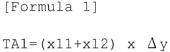
Equation 2
- Here, TA1 and TA2 designate the first and second planar areas, respectively, x11 designates the length of an upper end portion of the
insulation layer 114 that is covered by thepackage body 110 along the x-axis, x12 designates the length of a lower end portion of theinsulation layer 114 that is covered by thepackage body 110 along the x-axis, x2 designates the length of a portion of theinsulation layer 114 that is not covered by thepackage body 110 and is exposed along the x-axis, and Δy designates the length of theinsulation layer 114 along the y-axis. In the case of the light-emittingdevice package 100A according to the embodiment, x2 is "0". - In addition, referring to
FIGs. 15 and17 , thepackage body 110 is illustrated as exposing a middle portion of theinsulation layer 114. Thus, the distance x11 or x12 from the tip end of the exposedinsulation layer 114 to the edge of the cavity C may be greater than "0", but the embodiment is not limited thereto. According to another embodiment, x11 or x12 may be "0". - As described above, so long as the exposed portion of the bottom surface of the cavity C (i.e. the exposed front surface of at least one of the first or second lead frame LF1 or LF2) is minimized, thereby increasing the surface area of the
inclined surface 112 so as to increase light extraction efficiency and so long as the length of the introduction path of the outside air is increased so as to increase the reliability and and so as to secure rigidity of the light-emitting device package, thepackage body 110 may cover theentire insulation layer 114, as in the light-emittingdevice package 100A according to the embodiment, or may cover only a portion of theinsulation layer 114, as in the light-emitting device packages 100B and 100C according to the other embodiments. To this end, the first planar area TA1 may be equal to or greater than the second planar area TA2, but the embodiment is not limited thereto. In addition, in the case of the light-emittingdevice package 100A according to the embodiment, since thepackage body 110 covers theentire insulation layer 114 and there is no exposedinsulation layer 114 that is not covered with thepackage body 110, the second planar area becomes "0". Therefore, even in the case of the light-emittingdevice package 100A according to the embodiment, it can be appreciated that the first planar area is greater than the second planar area. - In conclusion, compared to the case where the first planar area is smaller than the second planar area, since, when the first planar area is equal to or greater than the second planar area, as in the embodiment, the surface area of the
inclined surface 112, which has reflectance greater than the reflectance of the bottom surface of the cavity C, increases, light extraction efficiency may be increased and the rigidity of the lead frames LF1 and LF2 may be increased. - In addition, in the light-emitting device packages 100A, 100B and 100C according to the above-described embodiments, for example, referring to
FIG. 11 , the top surface LFT1 of the first lead frame LF1, the top surface LFT2 of the second lead frame LF2, and thetop surface 114T of theinsulation layer 114 may not be stepped, but may be disposed in the same plane, but the embodiment is not limited thereto. That is, according to another embodiment, the top surface LFT1 of the first lead frame LF1, the top surface LFT2 of the second lead frame LF2, and thetop surface 114T of theinsulation layer 114 may be stepped, unlike the illustration. - Meanwhile, for the convenience of description, the illustration of the
molding member 150 is omitted inFIGs. 1 ,6a ,6b ,9 , and14 to 17 . However, as illustrated inFIGs. 8 ,11 ,12, 13 , and18 to 20 , the light-emitting device packages 100A, 100B and 100C according to the embodiments may further include themolding member 150. Themolding member 150 may surround and protect the light-emittingdevices - The
molding member 150 may be formed of, for example, a transparent polymer resin such as silicon (Si), and may include phosphors, and therefore may change the wavelength of the light emitted from the light-emittingdevices devices - The YGA-based and TAG-based fluorescent substances may be selected and used from among (Y, Tb, Lu, Sc, La, Gd, Sm)3(Al, Ga, In, Si, Fe)5(O, S)12:Ce, and the silicate-based fluorescent substance may be selected and used from among (Sr, Ba, Ca, Mg)2SiO4: (Eu, F, Cl).
- In addition, the sulfide-based fluorescent substance may be selected and used from among (Ca, Sr)S:Eu, (Sr, Ca, Ba)(Al, Ga)2S4: Eu, and the nitride-based phosphors are at least one material of (Sr, Ca, Si, Al, 0)N:Eu (e.g. CaAlSiN4:Eu β-SiAlON:Eu) or Ca-α SiAlON:Eu-based (Cax, My)(Si, Al)12(O, N)16 (here, M is at least one material of Eu, Tb, Yb or Er, 0.05<(x+y)<0.3, 0.02<X<0.27 and 0.03<y<0.3).
- Red phosphors may include nitride-based phosphors including N(e.g. CaAlSiN3:Eu). Such nitride-based red phosphors may have higher reliability to withstand external environments such as heat and moisture and lower discoloration possibility than sulfide-based phosphors.
- The light-emitting device packages 100A, 100B and 100C may further include a lens (not illustrated) disposed on the
molding member 150. The lens (not illustrated) may adjust the distribution of light emitted from the light-emitting device packages 100A, 100B and 100C. - A plurality of light-emitting device packages according to the embodiments may be disposed on a substrate to form an array, and optical members, such as a light guide plate, a prism sheet, and a diffusion sheet may be disposed on the optical path of the light-emitting device packages. The light-emitting device packages, the substrate, and the optical members may function as a backlight unit.
- In addition, a display apparatus, an indicator apparatus, and a lighting apparatus including the light-emitting device packages according to the embodiments may be realized.
- Here, the display apparatus may include a bottom cover, a reflector disposed on the bottom cover, a light-emitting module configured to emit light, a light guide plate disposed in front of the reflector to forwardly guide the light emitted from the light-emitting module, optical sheets including prism sheets disposed in front of the light guide plate, a display panel disposed in front of the optical sheets, an image signal output circuit connected to the display panel so as to supply an image signal to the display panel, and a color filter disposed in front of the display panel. Here, the bottom cover, the reflector, the light-emitting module, the light guide plate, and the optical sheets may construct a backlight unit.
- In addition, the lighting apparatus may include a light source module having a substrate and a light-emitting device package according to the embodiments, a heat radiator configured to dissipate heat from the light source module, and a power supply unit configured to process or convert an electric signal provided from the outside so as to supply the same to the light source module. For example, the lighting apparatus may include a lamp, a headlamp, or a street light.
- The head lamp may include a light-emitting module, which includes light-emitting device packages disposed on a substrate, a reflector, which reflects light emitted from the light-emitting module in a given direction, for example, in a forward direction, a lens, which forwardly refracts the light reflected by the reflector, and a shade, which blocks or reflects some of the light, which has been reflected by the reflector and directed to the lens, so as to achieve the light distribution pattern desired by a designer.
- Although embodiments have been described above, the above description is merely given by way of example and is not intended to limit the disclosure, and it will be apparent to those skilled in the art that various modifications and applications, which are not exemplified above, may be devised without departing from the essential characteristics of the embodiments. For example, the respective constituent devices described in the embodiments may be modified in various ways. In addition, differences associated with these modifications and alterations should be interpreted as being included in the scope of the disclosure defined by the accompanying claims.
- Modes for the implementation of embodiments have sufficiently been described in the "best mode" described above.
- A light-emitting device package according to embodiments may be used in a display apparatus, an indicator apparatus, and a lighting apparatus.
Claims (20)
- A light-emitting device package, comprising;
first and second lead frames;
an insulation layer disposed between the first and second lead frames to electrically insulate the first and second lead frames from each other;
a package body configured to expose a portion of a front surface of at least one of the first or second lead frame;
a light-emitting device disposed on the exposed front surface of at least one of the first or second lead frame and having first and second electrodes electrically connected to the respective first and second lead frames; and
a Zener diode disposed on the first lead frame so as to be spaced apart from the light-emitting device with the package body interposed therebetween,
wherein the package body defines a cavity together with the exposed front surface of at least one of the first or second lead frame,
wherein the cavity has an inclined surface configured to reflect light emitted from the light-emitting device, and a lower end of the inclined surface is spaced apart from the light-emitting device, which is disposed on a bottom surface of the cavity, by a predetermined distance, and
wherein the package body disposed between the Zener diode and the light-emitting device has a thickness greater than a thickness of the Zener diode or a thickness of the light-emitting device. - The package according to claim 1, further comprising a first wire having one end electrically connected to the first electrode of the light-emitting device and a remaining end electrically connected to the first lead frame.
- The package according to claim 2, further comprising a second wire having one end electrically connected to the second electrode of the light-emitting device and a remaining end electrically connected to the second lead frame.
- The package according to claim 2, wherein the second electrode of the light-emitting device is directly electrically connected to the second lead frame.
- The package according to any one of claims 1 to 4, wherein the exposed front surface of the second lead frame comprises a first device area in which the light-emitting device is disposed.
- The package according to claim 5, wherein the exposed front surface of the second lead frame further comprises a first bonding area, which is electrically connected to the remaining end of the second wire and which is close to the first device area.
- The package according to claim 6, wherein the package body comprises a first groove configured to expose the first bonding area.
- The package according to claim 2, wherein the first lead frame comprises a second bonding area, which is not covered by the package body and is exposed and which is connected to the remaining end of the first wire.
- The package according to claim 8, wherein the package body comprises a second groove configured to expose the second bonding area.
- The package according to claim 8, wherein the package body comprises a first blind hole configured to expose the second bonding area.
- The package according to claim 1, wherein the predetermined distance is 30 µm, and the thickness of the package body disposed between the Zener diode and the light-emitting device is greater than 50 µm and is equal to or less than 200µm.
- The package according to any one of claims 1 to 4 and 8 to 11, further comprising a third wire having one end electrically connected to the Zener diode and a remaining end electrically connected to the second lead frame.
- The package according to claim 12, wherein the exposed front surface of the second lead frame comprises a third bonding area connected to the remaining end of the third wire.
- The package according to claim 13, wherein the package body comprises a third groove configured to expose the third bonding area.
- The package according to claim 12, wherein the first lead frame comprises a second device area in which the Zener diode is disposed.
- The package according to claim 15, wherein the package body comprises a second blind hole configured to expose a portion that is to be connected to the one end of the third wire.
- The package according to claim 1, wherein at least a portion of the insulation layer that is covered with the package body has a first planar area, which is equal to or greater than a second planar area of an exposed remaining portion of the insulation layer that is not covered by the package body.
- The package according to claim 1, wherein the package body defines the cavity together with the exposed front surface of at least one of the first or second lead frame and comprises an inclined surface configured to reflect the light emitted from the light-emitting device, and the light-emitting device is disposed inside the cavity, and
wherein the inclined surface has reflectance higher than reflectance of the exposed front surface of at least one of the first or second lead frame. - The package according to claim 18, wherein the package body further comprises a stepped portion disposed between the lower end of the inclined surface and the bottom surface of the cavity.
- The package according to claim 19, wherein the light-emitting device comprises first and second conductive semiconductor layers and an active layer disposed between the first and second conductive semiconductor layers, and
wherein a first height from the bottom surface of the cavity to a top surface of the stepped portion is smaller than a second height from the bottom surface of the cavity to the active layer.
Applications Claiming Priority (2)
| Application Number | Priority Date | Filing Date | Title |
|---|---|---|---|
| KR20150100967 | 2015-07-16 | ||
| PCT/KR2016/007773 WO2017010851A1 (en) | 2015-07-16 | 2016-07-18 | Light-emitting element package |
Publications (3)
| Publication Number | Publication Date |
|---|---|
| EP3324452A1 true EP3324452A1 (en) | 2018-05-23 |
| EP3324452A4 EP3324452A4 (en) | 2019-01-16 |
| EP3324452B1 EP3324452B1 (en) | 2021-04-28 |
Family
ID=57757091
Family Applications (1)
| Application Number | Title | Priority Date | Filing Date |
|---|---|---|---|
| EP16824766.6A Active EP3324452B1 (en) | 2015-07-16 | 2016-07-18 | Light-emitting element package |
Country Status (6)
| Country | Link |
|---|---|
| US (2) | US10424704B2 (en) |
| EP (1) | EP3324452B1 (en) |
| KR (1) | KR102034715B1 (en) |
| CN (1) | CN107851698B (en) |
| DE (1) | DE202016008796U1 (en) |
| WO (1) | WO2017010851A1 (en) |
Cited By (1)
| Publication number | Priority date | Publication date | Assignee | Title |
|---|---|---|---|---|
| JP2021044414A (en) * | 2019-09-12 | 2021-03-18 | 日亜化学工業株式会社 | Light emitting device |
Families Citing this family (6)
| Publication number | Priority date | Publication date | Assignee | Title |
|---|---|---|---|---|
| JP6729254B2 (en) * | 2016-09-30 | 2020-07-22 | 日亜化学工業株式会社 | Light emitting device and display device |
| JP6760324B2 (en) * | 2018-03-27 | 2020-09-23 | 日亜化学工業株式会社 | Light emitting device |
| KR102861696B1 (en) * | 2018-09-07 | 2025-09-18 | 서울반도체 주식회사 | Light emitting diode package |
| JP7295426B2 (en) * | 2019-09-13 | 2023-06-21 | 日亜化学工業株式会社 | light emitting device |
| JP7513878B2 (en) * | 2020-09-15 | 2024-07-10 | 日亜化学工業株式会社 | Light-emitting device |
| JP2023085831A (en) * | 2021-12-09 | 2023-06-21 | ローム株式会社 | semiconductor light emitting device |
Family Cites Families (34)
| Publication number | Priority date | Publication date | Assignee | Title |
|---|---|---|---|---|
| JPS5034686B1 (en) | 1969-07-30 | 1975-11-11 | ||
| DE10041686A1 (en) * | 2000-08-24 | 2002-03-14 | Osram Opto Semiconductors Gmbh | Component with a large number of LED chips |
| KR100632002B1 (en) * | 2005-08-02 | 2006-10-09 | 삼성전기주식회사 | Side type light emitting diode with protective element |
| JP5034686B2 (en) | 2006-11-22 | 2012-09-26 | 日亜化学工業株式会社 | Semiconductor device |
| TWM318795U (en) * | 2006-12-18 | 2007-09-11 | Lighthouse Technology Co Ltd | Package structure |
| JP5168152B2 (en) | 2006-12-28 | 2013-03-21 | 日亜化学工業株式会社 | Light emitting device |
| TWI329934B (en) * | 2007-01-17 | 2010-09-01 | Chi Mei Lighting Tech Corp | Lead frame structure of light emitting diode |
| KR101309761B1 (en) | 2007-03-29 | 2013-09-17 | 서울반도체 주식회사 | Light emitting element |
| KR20090044306A (en) | 2007-10-31 | 2009-05-07 | 서울반도체 주식회사 | Light emitting diode package |
| DE102007060206A1 (en) | 2007-12-14 | 2009-06-18 | Osram Opto Semiconductors Gmbh | Arrangement with at least one optoelectronic semiconductor component |
| KR101007131B1 (en) | 2008-11-25 | 2011-01-10 | 엘지이노텍 주식회사 | Light emitting device package |
| KR101064072B1 (en) * | 2009-02-24 | 2011-09-08 | 엘지이노텍 주식회사 | Light emitting device package |
| JP5310672B2 (en) * | 2009-10-15 | 2013-10-09 | 日亜化学工業株式会社 | Light emitting device and manufacturing method thereof |
| KR20110067388A (en) | 2009-12-14 | 2011-06-22 | 엘지디스플레이 주식회사 | Light emitting diodes and manufacturing method thereof |
| CN102456826A (en) * | 2010-11-01 | 2012-05-16 | 富士康(昆山)电脑接插件有限公司 | LED (Light-Emitting Diode) lead frame |
| CN102130273A (en) | 2010-12-10 | 2011-07-20 | 深圳市华星光电技术有限公司 | Light emitting diode packaging structure |
| JP2014038876A (en) * | 2010-12-15 | 2014-02-27 | Panasonic Corp | Semiconductor light-emitting device |
| KR20120079668A (en) | 2011-01-05 | 2012-07-13 | 삼성엘이디 주식회사 | Led package and method thereof |
| KR20120082192A (en) | 2011-01-13 | 2012-07-23 | 삼성엘이디 주식회사 | Light emitting device package |
| US8987022B2 (en) | 2011-01-17 | 2015-03-24 | Samsung Electronics Co., Ltd. | Light-emitting device package and method of manufacturing the same |
| KR20120118686A (en) * | 2011-04-19 | 2012-10-29 | 엘지이노텍 주식회사 | Light emitting device module |
| KR101788723B1 (en) * | 2011-04-28 | 2017-10-20 | 엘지이노텍 주식회사 | Light emitting device package |
| KR101923688B1 (en) | 2011-08-29 | 2018-11-29 | 엘지이노텍 주식회사 | Light emitting device package and light unit |
| ITRM20110475A1 (en) * | 2011-09-09 | 2013-03-10 | Probiotical Spa | BACTERIA OF LACTIC AND / OR BIFIED BACTERIA BACTERIA, OPTIONALLY ADDED TO N-ACETYLCISTEIN AND / OR LYSOZYME MICROINCAPSULATE GASTROPROTETTO, HAVING INHIBITION ACTIVITIES / REDUCTION OF THE GROWTH OF DIFFERENT E.COLI BIOTYPES, INCLUDING E.COLI O157: H7 E |
| KR101905535B1 (en) * | 2011-11-16 | 2018-10-10 | 엘지이노텍 주식회사 | Light emitting device and light apparatus having thereof |
| KR20130054866A (en) * | 2011-11-17 | 2013-05-27 | 엘지이노텍 주식회사 | The light emitting device package and the light emitting system |
| CN103187485A (en) * | 2011-12-27 | 2013-07-03 | 展晶科技(深圳)有限公司 | Manufacturing method of light emitting diode |
| KR20120030475A (en) * | 2012-01-27 | 2012-03-28 | 서울반도체 주식회사 | Light emitting diode package |
| KR20140029617A (en) * | 2012-08-29 | 2014-03-11 | 엘지이노텍 주식회사 | A light emitting device package |
| KR101337599B1 (en) | 2012-12-17 | 2013-12-06 | 서울반도체 주식회사 | Light emitting diode |
| JP6107136B2 (en) * | 2012-12-29 | 2017-04-05 | 日亜化学工業株式会社 | LIGHT EMITTING DEVICE PACKAGE, LIGHT EMITTING DEVICE INCLUDING THE SAME, AND LIGHTING DEVICE EQUIPPED WITH THE LIGHT EMITTING DEVICE |
| KR102053287B1 (en) | 2013-04-29 | 2019-12-06 | 엘지이노텍 주식회사 | Light emitting device and lighting system |
| JP6176101B2 (en) * | 2013-12-17 | 2017-08-09 | 日亜化学工業株式会社 | Resin package and light emitting device |
| KR101633046B1 (en) | 2015-01-13 | 2016-06-23 | 루미마이크로 주식회사 | Light emitting device package |
-
2016
- 2016-07-18 KR KR1020167024032A patent/KR102034715B1/en not_active Expired - Fee Related
- 2016-07-18 CN CN201680041607.1A patent/CN107851698B/en active Active
- 2016-07-18 EP EP16824766.6A patent/EP3324452B1/en active Active
- 2016-07-18 DE DE202016008796.8U patent/DE202016008796U1/en not_active Expired - Lifetime
- 2016-07-18 US US15/744,698 patent/US10424704B2/en active Active
- 2016-07-18 WO PCT/KR2016/007773 patent/WO2017010851A1/en not_active Ceased
-
2019
- 2019-03-15 US US16/355,012 patent/US10998476B2/en active Active
Cited By (1)
| Publication number | Priority date | Publication date | Assignee | Title |
|---|---|---|---|---|
| JP2021044414A (en) * | 2019-09-12 | 2021-03-18 | 日亜化学工業株式会社 | Light emitting device |
Also Published As
| Publication number | Publication date |
|---|---|
| WO2017010851A1 (en) | 2017-01-19 |
| CN107851698B (en) | 2020-08-04 |
| US10998476B2 (en) | 2021-05-04 |
| US10424704B2 (en) | 2019-09-24 |
| US20180212117A1 (en) | 2018-07-26 |
| EP3324452B1 (en) | 2021-04-28 |
| US20190259929A1 (en) | 2019-08-22 |
| EP3324452A4 (en) | 2019-01-16 |
| DE202016008796U1 (en) | 2019-10-24 |
| KR20180020854A (en) | 2018-02-28 |
| KR102034715B1 (en) | 2019-10-22 |
| CN107851698A (en) | 2018-03-27 |
Similar Documents
| Publication | Publication Date | Title |
|---|---|---|
| US10475978B2 (en) | Light emitting device package having improved reliability, and lighting apparatus including the package | |
| US10998478B2 (en) | Light-emitting element, light-emitting element package comprising light-emitting element, and light-emitting device comprising light-emitting element package | |
| US10205058B2 (en) | Light-emitting device package and light-emitting apparatus comprising same | |
| US10998476B2 (en) | Light-emitting device package | |
| KR102038443B1 (en) | Light emitting device and light emitting device package | |
| EP2830094B1 (en) | Light emitting device | |
| KR102080775B1 (en) | Light emitting device | |
| KR20140059985A (en) | Light emitting device | |
| EP2860770B1 (en) | Light-emitting element | |
| US10535804B2 (en) | Light-emitting device package | |
| US10546986B2 (en) | Light-emitting device package and light-emitting apparatus comprising same | |
| US10593848B2 (en) | Light emitting device package and light emitting apparatus | |
| KR102175341B1 (en) | Light emitting device, method for fabricating the same, and light emitting device package | |
| KR20190008402A (en) | Light emitting device package and lighting apparatus | |
| KR20130125458A (en) | Light emitting device package |
Legal Events
| Date | Code | Title | Description |
|---|---|---|---|
| REG | Reference to a national code |
Ref country code: DE Ref legal event code: R138 Ref document number: 202016008796 Country of ref document: DE Free format text: GERMAN DOCUMENT NUMBER IS 602016057038 |
|
| STAA | Information on the status of an ep patent application or granted ep patent |
Free format text: STATUS: THE INTERNATIONAL PUBLICATION HAS BEEN MADE |
|
| PUAI | Public reference made under article 153(3) epc to a published international application that has entered the european phase |
Free format text: ORIGINAL CODE: 0009012 |
|
| STAA | Information on the status of an ep patent application or granted ep patent |
Free format text: STATUS: REQUEST FOR EXAMINATION WAS MADE |
|
| 17P | Request for examination filed |
Effective date: 20180213 |
|
| AK | Designated contracting states |
Kind code of ref document: A1 Designated state(s): AL AT BE BG CH CY CZ DE DK EE ES FI FR GB GR HR HU IE IS IT LI LT LU LV MC MK MT NL NO PL PT RO RS SE SI SK SM TR |
|
| AX | Request for extension of the european patent |
Extension state: BA ME |
|
| DAV | Request for validation of the european patent (deleted) | ||
| DAX | Request for extension of the european patent (deleted) | ||
| A4 | Supplementary search report drawn up and despatched |
Effective date: 20181219 |
|
| RIC1 | Information provided on ipc code assigned before grant |
Ipc: H01L 25/16 20060101ALI20181213BHEP Ipc: H01L 33/48 20100101ALI20181213BHEP Ipc: H01L 33/62 20100101AFI20181213BHEP Ipc: H01L 33/36 20100101ALI20181213BHEP Ipc: H01L 33/60 20100101ALI20181213BHEP Ipc: H01L 33/52 20100101ALI20181213BHEP |
|
| STAA | Information on the status of an ep patent application or granted ep patent |
Free format text: STATUS: EXAMINATION IS IN PROGRESS |
|
| 17Q | First examination report despatched |
Effective date: 20190618 |
|
| GRAP | Despatch of communication of intention to grant a patent |
Free format text: ORIGINAL CODE: EPIDOSNIGR1 |
|
| STAA | Information on the status of an ep patent application or granted ep patent |
Free format text: STATUS: GRANT OF PATENT IS INTENDED |
|
| INTG | Intention to grant announced |
Effective date: 20201119 |
|
| GRAS | Grant fee paid |
Free format text: ORIGINAL CODE: EPIDOSNIGR3 |
|
| GRAA | (expected) grant |
Free format text: ORIGINAL CODE: 0009210 |
|
| STAA | Information on the status of an ep patent application or granted ep patent |
Free format text: STATUS: THE PATENT HAS BEEN GRANTED |
|
| AK | Designated contracting states |
Kind code of ref document: B1 Designated state(s): AL AT BE BG CH CY CZ DE DK EE ES FI FR GB GR HR HU IE IS IT LI LT LU LV MC MK MT NL NO PL PT RO RS SE SI SK SM TR |
|
| REG | Reference to a national code |
Ref country code: GB Ref legal event code: FG4D |
|
| REG | Reference to a national code |
Ref country code: CH Ref legal event code: EP |
|
| REG | Reference to a national code |
Ref country code: AT Ref legal event code: REF Ref document number: 1388100 Country of ref document: AT Kind code of ref document: T Effective date: 20210515 |
|
| REG | Reference to a national code |
Ref country code: DE Ref legal event code: R096 Ref document number: 602016057038 Country of ref document: DE |
|
| REG | Reference to a national code |
Ref country code: IE Ref legal event code: FG4D |
|
| RAP2 | Party data changed (patent owner data changed or rights of a patent transferred) |
Owner name: SUZHOU LEKIN SEMICONDUCTOR CO., LTD. |
|
| REG | Reference to a national code |
Ref country code: LT Ref legal event code: MG9D |
|
| REG | Reference to a national code |
Ref country code: DE Ref legal event code: R081 Ref document number: 602016057038 Country of ref document: DE Owner name: SUZHOU LEKIN SEMICONDUCTOR CO. LTD., TAICANG, CN Free format text: FORMER OWNER: LG INNOTEK CO., LTD., SEOUL, KR |
|
| REG | Reference to a national code |
Ref country code: AT Ref legal event code: MK05 Ref document number: 1388100 Country of ref document: AT Kind code of ref document: T Effective date: 20210428 |
|
| PG25 | Lapsed in a contracting state [announced via postgrant information from national office to epo] |
Ref country code: FI Free format text: LAPSE BECAUSE OF FAILURE TO SUBMIT A TRANSLATION OF THE DESCRIPTION OR TO PAY THE FEE WITHIN THE PRESCRIBED TIME-LIMIT Effective date: 20210428 Ref country code: NL Free format text: LAPSE BECAUSE OF FAILURE TO SUBMIT A TRANSLATION OF THE DESCRIPTION OR TO PAY THE FEE WITHIN THE PRESCRIBED TIME-LIMIT Effective date: 20210428 Ref country code: LT Free format text: LAPSE BECAUSE OF FAILURE TO SUBMIT A TRANSLATION OF THE DESCRIPTION OR TO PAY THE FEE WITHIN THE PRESCRIBED TIME-LIMIT Effective date: 20210428 Ref country code: BG Free format text: LAPSE BECAUSE OF FAILURE TO SUBMIT A TRANSLATION OF THE DESCRIPTION OR TO PAY THE FEE WITHIN THE PRESCRIBED TIME-LIMIT Effective date: 20210728 Ref country code: AT Free format text: LAPSE BECAUSE OF FAILURE TO SUBMIT A TRANSLATION OF THE DESCRIPTION OR TO PAY THE FEE WITHIN THE PRESCRIBED TIME-LIMIT Effective date: 20210428 Ref country code: HR Free format text: LAPSE BECAUSE OF FAILURE TO SUBMIT A TRANSLATION OF THE DESCRIPTION OR TO PAY THE FEE WITHIN THE PRESCRIBED TIME-LIMIT Effective date: 20210428 |
|
| PG25 | Lapsed in a contracting state [announced via postgrant information from national office to epo] |
Ref country code: PL Free format text: LAPSE BECAUSE OF FAILURE TO SUBMIT A TRANSLATION OF THE DESCRIPTION OR TO PAY THE FEE WITHIN THE PRESCRIBED TIME-LIMIT Effective date: 20210428 Ref country code: PT Free format text: LAPSE BECAUSE OF FAILURE TO SUBMIT A TRANSLATION OF THE DESCRIPTION OR TO PAY THE FEE WITHIN THE PRESCRIBED TIME-LIMIT Effective date: 20210830 Ref country code: NO Free format text: LAPSE BECAUSE OF FAILURE TO SUBMIT A TRANSLATION OF THE DESCRIPTION OR TO PAY THE FEE WITHIN THE PRESCRIBED TIME-LIMIT Effective date: 20210728 Ref country code: RS Free format text: LAPSE BECAUSE OF FAILURE TO SUBMIT A TRANSLATION OF THE DESCRIPTION OR TO PAY THE FEE WITHIN THE PRESCRIBED TIME-LIMIT Effective date: 20210428 Ref country code: SE Free format text: LAPSE BECAUSE OF FAILURE TO SUBMIT A TRANSLATION OF THE DESCRIPTION OR TO PAY THE FEE WITHIN THE PRESCRIBED TIME-LIMIT Effective date: 20210428 Ref country code: IS Free format text: LAPSE BECAUSE OF FAILURE TO SUBMIT A TRANSLATION OF THE DESCRIPTION OR TO PAY THE FEE WITHIN THE PRESCRIBED TIME-LIMIT Effective date: 20210828 Ref country code: GR Free format text: LAPSE BECAUSE OF FAILURE TO SUBMIT A TRANSLATION OF THE DESCRIPTION OR TO PAY THE FEE WITHIN THE PRESCRIBED TIME-LIMIT Effective date: 20210729 Ref country code: LV Free format text: LAPSE BECAUSE OF FAILURE TO SUBMIT A TRANSLATION OF THE DESCRIPTION OR TO PAY THE FEE WITHIN THE PRESCRIBED TIME-LIMIT Effective date: 20210428 |
|
| REG | Reference to a national code |
Ref country code: NL Ref legal event code: MP Effective date: 20210428 |
|
| PG25 | Lapsed in a contracting state [announced via postgrant information from national office to epo] |
Ref country code: ES Free format text: LAPSE BECAUSE OF FAILURE TO SUBMIT A TRANSLATION OF THE DESCRIPTION OR TO PAY THE FEE WITHIN THE PRESCRIBED TIME-LIMIT Effective date: 20210428 Ref country code: RO Free format text: LAPSE BECAUSE OF FAILURE TO SUBMIT A TRANSLATION OF THE DESCRIPTION OR TO PAY THE FEE WITHIN THE PRESCRIBED TIME-LIMIT Effective date: 20210428 Ref country code: CZ Free format text: LAPSE BECAUSE OF FAILURE TO SUBMIT A TRANSLATION OF THE DESCRIPTION OR TO PAY THE FEE WITHIN THE PRESCRIBED TIME-LIMIT Effective date: 20210428 Ref country code: DK Free format text: LAPSE BECAUSE OF FAILURE TO SUBMIT A TRANSLATION OF THE DESCRIPTION OR TO PAY THE FEE WITHIN THE PRESCRIBED TIME-LIMIT Effective date: 20210428 Ref country code: EE Free format text: LAPSE BECAUSE OF FAILURE TO SUBMIT A TRANSLATION OF THE DESCRIPTION OR TO PAY THE FEE WITHIN THE PRESCRIBED TIME-LIMIT Effective date: 20210428 Ref country code: SK Free format text: LAPSE BECAUSE OF FAILURE TO SUBMIT A TRANSLATION OF THE DESCRIPTION OR TO PAY THE FEE WITHIN THE PRESCRIBED TIME-LIMIT Effective date: 20210428 Ref country code: SM Free format text: LAPSE BECAUSE OF FAILURE TO SUBMIT A TRANSLATION OF THE DESCRIPTION OR TO PAY THE FEE WITHIN THE PRESCRIBED TIME-LIMIT Effective date: 20210428 |
|
| REG | Reference to a national code |
Ref country code: DE Ref legal event code: R097 Ref document number: 602016057038 Country of ref document: DE |
|
| REG | Reference to a national code |
Ref country code: CH Ref legal event code: PL |
|
| PLBE | No opposition filed within time limit |
Free format text: ORIGINAL CODE: 0009261 |
|
| STAA | Information on the status of an ep patent application or granted ep patent |
Free format text: STATUS: NO OPPOSITION FILED WITHIN TIME LIMIT |
|
| GBPC | Gb: european patent ceased through non-payment of renewal fee |
Effective date: 20210728 |
|
| PG25 | Lapsed in a contracting state [announced via postgrant information from national office to epo] |
Ref country code: MC Free format text: LAPSE BECAUSE OF FAILURE TO SUBMIT A TRANSLATION OF THE DESCRIPTION OR TO PAY THE FEE WITHIN THE PRESCRIBED TIME-LIMIT Effective date: 20210428 |
|
| REG | Reference to a national code |
Ref country code: BE Ref legal event code: MM Effective date: 20210731 |
|
| 26N | No opposition filed |
Effective date: 20220131 |
|
| PG25 | Lapsed in a contracting state [announced via postgrant information from national office to epo] |
Ref country code: LI Free format text: LAPSE BECAUSE OF NON-PAYMENT OF DUE FEES Effective date: 20210731 Ref country code: GB Free format text: LAPSE BECAUSE OF NON-PAYMENT OF DUE FEES Effective date: 20210728 Ref country code: CH Free format text: LAPSE BECAUSE OF NON-PAYMENT OF DUE FEES Effective date: 20210731 |
|
| PG25 | Lapsed in a contracting state [announced via postgrant information from national office to epo] |
Ref country code: IS Free format text: LAPSE BECAUSE OF FAILURE TO SUBMIT A TRANSLATION OF THE DESCRIPTION OR TO PAY THE FEE WITHIN THE PRESCRIBED TIME-LIMIT Effective date: 20210828 Ref country code: LU Free format text: LAPSE BECAUSE OF NON-PAYMENT OF DUE FEES Effective date: 20210718 Ref country code: FR Free format text: LAPSE BECAUSE OF NON-PAYMENT OF DUE FEES Effective date: 20210731 Ref country code: AL Free format text: LAPSE BECAUSE OF FAILURE TO SUBMIT A TRANSLATION OF THE DESCRIPTION OR TO PAY THE FEE WITHIN THE PRESCRIBED TIME-LIMIT Effective date: 20210428 |
|
| PG25 | Lapsed in a contracting state [announced via postgrant information from national office to epo] |
Ref country code: IT Free format text: LAPSE BECAUSE OF FAILURE TO SUBMIT A TRANSLATION OF THE DESCRIPTION OR TO PAY THE FEE WITHIN THE PRESCRIBED TIME-LIMIT Effective date: 20210428 Ref country code: IE Free format text: LAPSE BECAUSE OF NON-PAYMENT OF DUE FEES Effective date: 20210718 Ref country code: BE Free format text: LAPSE BECAUSE OF NON-PAYMENT OF DUE FEES Effective date: 20210731 |
|
| PG25 | Lapsed in a contracting state [announced via postgrant information from national office to epo] |
Ref country code: HU Free format text: LAPSE BECAUSE OF FAILURE TO SUBMIT A TRANSLATION OF THE DESCRIPTION OR TO PAY THE FEE WITHIN THE PRESCRIBED TIME-LIMIT; INVALID AB INITIO Effective date: 20160718 |
|
| PG25 | Lapsed in a contracting state [announced via postgrant information from national office to epo] |
Ref country code: CY Free format text: LAPSE BECAUSE OF FAILURE TO SUBMIT A TRANSLATION OF THE DESCRIPTION OR TO PAY THE FEE WITHIN THE PRESCRIBED TIME-LIMIT Effective date: 20210428 |
|
| PGFP | Annual fee paid to national office [announced via postgrant information from national office to epo] |
Ref country code: DE Payment date: 20230607 Year of fee payment: 8 |
|
| PG25 | Lapsed in a contracting state [announced via postgrant information from national office to epo] |
Ref country code: MK Free format text: LAPSE BECAUSE OF FAILURE TO SUBMIT A TRANSLATION OF THE DESCRIPTION OR TO PAY THE FEE WITHIN THE PRESCRIBED TIME-LIMIT Effective date: 20210428 |
|
| PG25 | Lapsed in a contracting state [announced via postgrant information from national office to epo] |
Ref country code: MT Free format text: LAPSE BECAUSE OF FAILURE TO SUBMIT A TRANSLATION OF THE DESCRIPTION OR TO PAY THE FEE WITHIN THE PRESCRIBED TIME-LIMIT Effective date: 20210428 |
|
| REG | Reference to a national code |
Ref country code: DE Ref legal event code: R079 Ref document number: 602016057038 Country of ref document: DE Free format text: PREVIOUS MAIN CLASS: H01L0033620000 Ipc: H10H0020857000 |
|
| REG | Reference to a national code |
Ref country code: DE Ref legal event code: R119 Ref document number: 602016057038 Country of ref document: DE |
|
| PG25 | Lapsed in a contracting state [announced via postgrant information from national office to epo] |
Ref country code: DE Free format text: LAPSE BECAUSE OF NON-PAYMENT OF DUE FEES Effective date: 20250201 |
|
| PG25 | Lapsed in a contracting state [announced via postgrant information from national office to epo] |
Ref country code: TR Free format text: LAPSE BECAUSE OF FAILURE TO SUBMIT A TRANSLATION OF THE DESCRIPTION OR TO PAY THE FEE WITHIN THE PRESCRIBED TIME-LIMIT Effective date: 20210428 |