EP3324439A1 - Electrostatic-discharge protection circuit applied to integrated circuit - Google Patents
Electrostatic-discharge protection circuit applied to integrated circuit Download PDFInfo
- Publication number
- EP3324439A1 EP3324439A1 EP17794646.4A EP17794646A EP3324439A1 EP 3324439 A1 EP3324439 A1 EP 3324439A1 EP 17794646 A EP17794646 A EP 17794646A EP 3324439 A1 EP3324439 A1 EP 3324439A1
- Authority
- EP
- European Patent Office
- Prior art keywords
- voltage
- terminal
- protection circuit
- coupled
- esd protection
- Prior art date
- Legal status (The legal status is an assumption and is not a legal conclusion. Google has not performed a legal analysis and makes no representation as to the accuracy of the status listed.)
- Granted
Links
Images


Classifications
-
- H—ELECTRICITY
- H10—SEMICONDUCTOR DEVICES; ELECTRIC SOLID-STATE DEVICES NOT OTHERWISE PROVIDED FOR
- H10D—INORGANIC ELECTRIC SEMICONDUCTOR DEVICES
- H10D89/00—Aspects of integrated devices not covered by groups H10D84/00 - H10D88/00
- H10D89/60—Integrated devices comprising arrangements for electrical or thermal protection, e.g. protection circuits against electrostatic discharge [ESD]
- H10D89/601—Integrated devices comprising arrangements for electrical or thermal protection, e.g. protection circuits against electrostatic discharge [ESD] for devices having insulated gate electrodes, e.g. for IGFETs or IGBTs
- H10D89/811—Integrated devices comprising arrangements for electrical or thermal protection, e.g. protection circuits against electrostatic discharge [ESD] for devices having insulated gate electrodes, e.g. for IGFETs or IGBTs using FETs as protective elements
- H10D89/813—Integrated devices comprising arrangements for electrical or thermal protection, e.g. protection circuits against electrostatic discharge [ESD] for devices having insulated gate electrodes, e.g. for IGFETs or IGBTs using FETs as protective elements specially adapted to provide an electrical current path other than the field-effect induced current path
- H10D89/815—Integrated devices comprising arrangements for electrical or thermal protection, e.g. protection circuits against electrostatic discharge [ESD] for devices having insulated gate electrodes, e.g. for IGFETs or IGBTs using FETs as protective elements specially adapted to provide an electrical current path other than the field-effect induced current path involving a parasitic bipolar transistor triggered by the local electrical biasing of the layer acting as base region of said parasitic bipolar transistor
-
- H—ELECTRICITY
- H10—SEMICONDUCTOR DEVICES; ELECTRIC SOLID-STATE DEVICES NOT OTHERWISE PROVIDED FOR
- H10D—INORGANIC ELECTRIC SEMICONDUCTOR DEVICES
- H10D89/00—Aspects of integrated devices not covered by groups H10D84/00 - H10D88/00
- H10D89/60—Integrated devices comprising arrangements for electrical or thermal protection, e.g. protection circuits against electrostatic discharge [ESD]
- H10D89/601—Integrated devices comprising arrangements for electrical or thermal protection, e.g. protection circuits against electrostatic discharge [ESD] for devices having insulated gate electrodes, e.g. for IGFETs or IGBTs
- H10D89/711—Integrated devices comprising arrangements for electrical or thermal protection, e.g. protection circuits against electrostatic discharge [ESD] for devices having insulated gate electrodes, e.g. for IGFETs or IGBTs using bipolar transistors as protective elements
- H10D89/713—Integrated devices comprising arrangements for electrical or thermal protection, e.g. protection circuits against electrostatic discharge [ESD] for devices having insulated gate electrodes, e.g. for IGFETs or IGBTs using bipolar transistors as protective elements including a PNP transistor and a NPN transistor, wherein each of said transistors has its base region coupled to the collector region of the other transistor, e.g. silicon controlled rectifier [SCR] devices
-
- H—ELECTRICITY
- H02—GENERATION; CONVERSION OR DISTRIBUTION OF ELECTRIC POWER
- H02H—EMERGENCY PROTECTIVE CIRCUIT ARRANGEMENTS
- H02H9/00—Emergency protective circuit arrangements for limiting excess current or voltage without disconnection
- H02H9/04—Emergency protective circuit arrangements for limiting excess current or voltage without disconnection responsive to excess voltage
- H02H9/045—Emergency protective circuit arrangements for limiting excess current or voltage without disconnection responsive to excess voltage adapted to a particular application and not provided for elsewhere
- H02H9/046—Emergency protective circuit arrangements for limiting excess current or voltage without disconnection responsive to excess voltage adapted to a particular application and not provided for elsewhere responsive to excess voltage appearing at terminals of integrated circuits
-
- H—ELECTRICITY
- H10—SEMICONDUCTOR DEVICES; ELECTRIC SOLID-STATE DEVICES NOT OTHERWISE PROVIDED FOR
- H10D—INORGANIC ELECTRIC SEMICONDUCTOR DEVICES
- H10D84/00—Integrated devices formed in or on semiconductor substrates that comprise only semiconducting layers, e.g. on Si wafers or on GaAs-on-Si wafers
- H10D84/40—Integrated devices formed in or on semiconductor substrates that comprise only semiconducting layers, e.g. on Si wafers or on GaAs-on-Si wafers characterised by the integration of at least one component covered by groups H10D12/00 or H10D30/00 with at least one component covered by groups H10D10/00 or H10D18/00, e.g. integration of IGFETs with BJTs
- H10D84/401—Combinations of FETs or IGBTs with BJTs
- H10D84/403—Combinations of FETs or IGBTs with BJTs and with one or more of diodes, resistors or capacitors
- H10D84/409—Combinations of FETs or IGBTs with lateral BJTs and with one or more of diodes, resistors or capacitors
-
- H—ELECTRICITY
- H10—SEMICONDUCTOR DEVICES; ELECTRIC SOLID-STATE DEVICES NOT OTHERWISE PROVIDED FOR
- H10D—INORGANIC ELECTRIC SEMICONDUCTOR DEVICES
- H10D89/00—Aspects of integrated devices not covered by groups H10D84/00 - H10D88/00
- H10D89/60—Integrated devices comprising arrangements for electrical or thermal protection, e.g. protection circuits against electrostatic discharge [ESD]
- H10D89/601—Integrated devices comprising arrangements for electrical or thermal protection, e.g. protection circuits against electrostatic discharge [ESD] for devices having insulated gate electrodes, e.g. for IGFETs or IGBTs
- H10D89/611—Integrated devices comprising arrangements for electrical or thermal protection, e.g. protection circuits against electrostatic discharge [ESD] for devices having insulated gate electrodes, e.g. for IGFETs or IGBTs using diodes as protective elements
-
- H—ELECTRICITY
- H10—SEMICONDUCTOR DEVICES; ELECTRIC SOLID-STATE DEVICES NOT OTHERWISE PROVIDED FOR
- H10D—INORGANIC ELECTRIC SEMICONDUCTOR DEVICES
- H10D89/00—Aspects of integrated devices not covered by groups H10D84/00 - H10D88/00
- H10D89/60—Integrated devices comprising arrangements for electrical or thermal protection, e.g. protection circuits against electrostatic discharge [ESD]
- H10D89/601—Integrated devices comprising arrangements for electrical or thermal protection, e.g. protection circuits against electrostatic discharge [ESD] for devices having insulated gate electrodes, e.g. for IGFETs or IGBTs
- H10D89/811—Integrated devices comprising arrangements for electrical or thermal protection, e.g. protection circuits against electrostatic discharge [ESD] for devices having insulated gate electrodes, e.g. for IGFETs or IGBTs using FETs as protective elements
- H10D89/813—Integrated devices comprising arrangements for electrical or thermal protection, e.g. protection circuits against electrostatic discharge [ESD] for devices having insulated gate electrodes, e.g. for IGFETs or IGBTs using FETs as protective elements specially adapted to provide an electrical current path other than the field-effect induced current path
-
- H—ELECTRICITY
- H10—SEMICONDUCTOR DEVICES; ELECTRIC SOLID-STATE DEVICES NOT OTHERWISE PROVIDED FOR
- H10D—INORGANIC ELECTRIC SEMICONDUCTOR DEVICES
- H10D89/00—Aspects of integrated devices not covered by groups H10D84/00 - H10D88/00
- H10D89/60—Integrated devices comprising arrangements for electrical or thermal protection, e.g. protection circuits against electrostatic discharge [ESD]
- H10D89/601—Integrated devices comprising arrangements for electrical or thermal protection, e.g. protection circuits against electrostatic discharge [ESD] for devices having insulated gate electrodes, e.g. for IGFETs or IGBTs
- H10D89/811—Integrated devices comprising arrangements for electrical or thermal protection, e.g. protection circuits against electrostatic discharge [ESD] for devices having insulated gate electrodes, e.g. for IGFETs or IGBTs using FETs as protective elements
- H10D89/817—FETs in a Darlington configuration
-
- H—ELECTRICITY
- H10—SEMICONDUCTOR DEVICES; ELECTRIC SOLID-STATE DEVICES NOT OTHERWISE PROVIDED FOR
- H10D—INORGANIC ELECTRIC SEMICONDUCTOR DEVICES
- H10D89/00—Aspects of integrated devices not covered by groups H10D84/00 - H10D88/00
- H10D89/60—Integrated devices comprising arrangements for electrical or thermal protection, e.g. protection circuits against electrostatic discharge [ESD]
- H10D89/601—Integrated devices comprising arrangements for electrical or thermal protection, e.g. protection circuits against electrostatic discharge [ESD] for devices having insulated gate electrodes, e.g. for IGFETs or IGBTs
- H10D89/911—Integrated devices comprising arrangements for electrical or thermal protection, e.g. protection circuits against electrostatic discharge [ESD] for devices having insulated gate electrodes, e.g. for IGFETs or IGBTs using passive elements as protective elements
-
- H—ELECTRICITY
- H10—SEMICONDUCTOR DEVICES; ELECTRIC SOLID-STATE DEVICES NOT OTHERWISE PROVIDED FOR
- H10D—INORGANIC ELECTRIC SEMICONDUCTOR DEVICES
- H10D89/00—Aspects of integrated devices not covered by groups H10D84/00 - H10D88/00
- H10D89/60—Integrated devices comprising arrangements for electrical or thermal protection, e.g. protection circuits against electrostatic discharge [ESD]
- H10D89/601—Integrated devices comprising arrangements for electrical or thermal protection, e.g. protection circuits against electrostatic discharge [ESD] for devices having insulated gate electrodes, e.g. for IGFETs or IGBTs
- H10D89/921—Integrated devices comprising arrangements for electrical or thermal protection, e.g. protection circuits against electrostatic discharge [ESD] for devices having insulated gate electrodes, e.g. for IGFETs or IGBTs characterised by the configuration of the interconnections connecting the protective arrangements, e.g. ESD buses
-
- H—ELECTRICITY
- H10—SEMICONDUCTOR DEVICES; ELECTRIC SOLID-STATE DEVICES NOT OTHERWISE PROVIDED FOR
- H10D—INORGANIC ELECTRIC SEMICONDUCTOR DEVICES
- H10D62/00—Semiconductor bodies, or regions thereof, of devices having potential barriers
- H10D62/10—Shapes, relative sizes or dispositions of the regions of the semiconductor bodies; Shapes of the semiconductor bodies
- H10D62/17—Semiconductor regions connected to electrodes not carrying current to be rectified, amplified or switched, e.g. channel regions
- H10D62/177—Base regions of bipolar transistors, e.g. BJTs or IGBTs
- H10D62/184—Base regions of bipolar transistors, e.g. BJTs or IGBTs of lateral BJTs
-
- H—ELECTRICITY
- H10—SEMICONDUCTOR DEVICES; ELECTRIC SOLID-STATE DEVICES NOT OTHERWISE PROVIDED FOR
- H10D—INORGANIC ELECTRIC SEMICONDUCTOR DEVICES
- H10D62/00—Semiconductor bodies, or regions thereof, of devices having potential barriers
- H10D62/10—Shapes, relative sizes or dispositions of the regions of the semiconductor bodies; Shapes of the semiconductor bodies
- H10D62/17—Semiconductor regions connected to electrodes not carrying current to be rectified, amplified or switched, e.g. channel regions
- H10D62/351—Substrate regions of field-effect devices
- H10D62/357—Substrate regions of field-effect devices of FETs
- H10D62/364—Substrate regions of field-effect devices of FETs of IGFETs
- H10D62/378—Contact regions to the substrate regions
-
- H—ELECTRICITY
- H10—SEMICONDUCTOR DEVICES; ELECTRIC SOLID-STATE DEVICES NOT OTHERWISE PROVIDED FOR
- H10W—GENERIC PACKAGES, INTERCONNECTIONS, CONNECTORS OR OTHER CONSTRUCTIONAL DETAILS OF DEVICES COVERED BY CLASS H10
- H10W10/00—Isolation regions in semiconductor bodies between components of integrated devices
- H10W10/01—Manufacture or treatment
- H10W10/031—Manufacture or treatment of isolation regions comprising PN junctions
-
- H—ELECTRICITY
- H10—SEMICONDUCTOR DEVICES; ELECTRIC SOLID-STATE DEVICES NOT OTHERWISE PROVIDED FOR
- H10W—GENERIC PACKAGES, INTERCONNECTIONS, CONNECTORS OR OTHER CONSTRUCTIONAL DETAILS OF DEVICES COVERED BY CLASS H10
- H10W10/00—Isolation regions in semiconductor bodies between components of integrated devices
- H10W10/30—Isolation regions comprising PN junctions
Definitions
- the present invention relates to an electrostatic discharge (ESD) protection circuit, and more particularly, to an ESD protection circuit capable of preventing leakage current.
- ESD electrostatic discharge
- ESD Electro static discharge
- the ESD protection circuit in the art has unavoidable leakage current, which increases over all power consumption of the integrated circuit (IC). Therefore, how to prevent leakage current is a significant objective in the field.
- an ESD protection circuit including a first N-type transistor including a first gate terminal, coupled to a ground terminal; a first electrode terminal, coupled to the first gate terminal; and a second electrode terminal; a second N-type transistor including a second gate terminal, coupled to a metal pad; a third electrode terminal, coupled to the second gate terminal; a fourth electrode terminal, coupled to the second electrode terminal; and a fifth electrode terminal; and a high-voltage tracing circuit including a first input terminal, coupled to the metal pad, receiving a metal pad voltage; a second input terminal, receiving a supply voltage; and an output terminal, coupled to the fifth electrode terminal, configured to output a high-voltage tracing voltage, wherein the high-voltage tracing voltage is larger than or equal to the metal pad voltage.
- the high-voltage tracing circuit includes a first transistor including a first control terminal, coupled to the second input terminal; a first terminal, coupled to the first input terminal; and a second terminal, coupled to the output terminal; and a second transistor including a second control terminal, coupled to the first input terminal; a third terminal, coupled to the second input terminal; and a fourth terminal, coupled to the output terminal.
- the metal pad voltage is larger than the supply voltage
- the first transistor is conducted and the second transistor is cutoff.
- the first transistor is cutoff and the second transistor is conducted.
- the high-voltage tracing circuit further includes a diode, coupled between the first input terminal and the first terminal of the first transistor.
- the first N-type transistor further includes a first base terminal, coupled to the first electrode terminal.
- the second N-type transistor includes a first deep N-well, disposed under the third electrode terminal, the fourth electrode terminal and the fifth electrode terminal.
- the second N-type transistor further includes a first P-well, disposed between the third electrode terminal, the fourth electrode terminal and the first deep N-well.
- the second N-type transistor further includes a first N-well, and the first N-well is disposed by a side of the first P-well.
- the N-type region is formed as the fifth electrode terminal.
- a metal pad voltage of the metal pad is a positive ESD voltage
- a first current flows to the ground terminal through the first N-type transistor.
- the first N-type transistor is formed as a first bipolar transistor.
- a metal pad voltage of the metal pad is a negative ESD voltage
- a second current flows to the metal pad through the second N-type transistor.
- the second N-type transistor is formed as a second bipolar transistor.
- the high-voltage tracing voltage is a maximum voltage of the metal pad voltage and the supply voltage.
- the ESD protection circuit further includes a diode, coupled between the fifth electrode terminal of the second N-type transistor and the output terminal of the high-voltage tracing circuit.
- the diode includes a first terminal, coupled to the fifth electrode terminal of the second N-type transistor; and a second terminal, coupled to the output terminal of the high-voltage tracing circuit.
- the diode includes a second N-well, disposed under the first terminal and the second terminal.
- the diode includes a second P-well, disposed under the first terminal and the second terminal.
- the diode further includes a second deep N-well, disposed under the second P-well.
- the ESD protection circuit further includes a plurality of diodes, formed as a diode series; wherein the diode series is coupled between the fifth electrode terminal of the second N-type transistor and the output terminal of the high-voltage tracing circuit.
- the ESD protection circuit provided by the present application utilizes the high-voltage tracing circuit to avoid the leakage current, and has advantages of small circuit area and low power consumption.
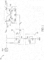
- FIG. 1 is a schematic diagram of an electrostatic discharge (ESD) protection circuit 10 according to an embodiment of the present invention
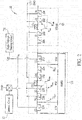
- FIG. 2 is a sectional side view of circuit layout regarding a first N-type transistor Q1 and a second N-type transistor Q2.
- the ESD protection circuit 10 includes the first N-type transistor Q1, the second N-type transistor Q2 and a high-voltage tracing circuit TH.
- the first N-type transistor Q1 includes a gate terminal G1 and electrode terminals S1 and D1.
- the second N-type transistor Q2 includes a gate terminal G2 and electrode terminals S2, D2 and E2.
- the gate terminal G1 and the electrode terminal S1 are coupled to a ground terminal GND.
- the gate terminal G2 and the electrode terminal S2 are coupled to a metal pad PAD.
- the electrode terminal D1 of the first N-type transistor Q1 is coupled to the electrode terminal D2 of the second N-type transistor.
- the high-voltage tracing circuit TH has input terminals In_1 and In_2 and an output terminal Out.
- the input terminal In_1 is coupled to the metal pad PAD, configured to receive a metal pad voltage VPAD.
- the input terminal In_2 is configured to receive a supply voltage VDDIO.
- the output terminal Out is coupled to the electrode terminal E2 of the second N-type transistor Q2, configured to output a high-voltage tracing voltage VE2, wherein the high-voltage tracing voltage VE2 is larger than or equal to the metal pad voltage VPAD.
- the first N-type transistor Q1 is formed on a P-type substrate PSUB. That is, the N-type regions 200, 202 and the P-type regions 204, 206 are formed on the P-type substrate PSUB.
- the N-type region 200 may be formed as the electrode terminal D1 of the first N-type transistor Q1.
- the N-type region 202 may be formed as the electrode terminal S1 of the first N-type transistor Q1.
- An oxide layer and a poly silicon layer, disposed between the N-type region 200 and the N-type region 202, are formed as the gate terminal G1 of the first N-type transistor Q1.
- the P-type region 204 may be formed as a base terminal B1 of the first N-type transistor Q1.
- the gate terminal G1, the electrode terminal S1 and the base terminal B1 of the first N-type transistor Q1 are all coupled to the ground terminal GND.
- the second N-type transistor Q2 includes a deep N-well DNW, a P-well PW, N-wells NW, N-type regions 220, 222, 227 and 228 and P-type regions 224 and 226.
- the P-well PW and the N-wells NW are both formed on the deep N-well DNW.
- the N-wells NW are disposed by two sides of the P-well PW.
- the N-type regions 220, 222 and the P-type regions 224 and 226 are formed on the P-well PW.
- the N-type regions 227 and 228 are formed on the N-wells NW.
- the N-type region 220 may be formed as the electrode terminal S2 of the second N-type transistor Q2, and the N-type region 222 may be formed as the electrode terminal D2 of the second N-type transistor Q2.
- the P-type region 226 may be formed as a base terminal B2 of the second N-type transistor Q2.
- the gate terminal G2, the electrode terminal S2 and the base terminal B2 of the second N-type transistor Q2 are all coupled to the metal pad PAD.
- the N-type regions 227 and 228 are formed as the electrode terminal E2 of the second N-type transistor Q2, and coupled to the output terminal Out of the high-voltage tracing circuit TH.
- junctions between the P-well PW of the second N-type transistor Q2 and the N-well NW would form parasitic diodes Dpar.
- the forward bias between the P-well PW and the N-wells NW is too large, it is equivalent that the parasitic diodes Dpar are conducted, and leakage current from the P-well PW to the N-wells NW is generated.
- the high-voltage tracing circuit TH may output the high-voltage tracing voltage VE2 which is larger than or equal to the metal pad voltage VPAD, to prevent the leakage current.
- the high-voltage tracing circuit TH includes a first transistor P1 and a second transistor P2.
- the first transistor P1 and the second transistor P2 are all PMOS.
- a gate PG1 of the first transistor P1 is coupled to the input terminal In_2 to receive the supply voltage VDDIO.
- a source PS1 of the first transistor P1 is coupled to the input terminal In_1 to receive the metal pad voltage VPAD.
- a gate PG2 of the second transistor P2 is coupled to the input terminal In_1 to receive the metal pad voltage VPAD.
- a source PS2 of the second transistor P2 is coupled to the input terminal In_2 to receive the supply voltage VDDIO, a drain PD1 of the first transistor P1 and a drain PD2 of the second transistor P2 are both coupled to the electrode terminal E2 of the second N-type transistor Q2. Ignoring a threshold voltage Vth of the first transistor P1 and the second transistor P2, when the metal pad voltage VPAD is larger than the supply voltage VDDIO, the first transistor P1 is conducted and the second transistor P2 is cutoff. At this time, the high-voltage tracing circuit TH outputs the high-voltage tracing voltage VE2 as the metal pad voltage VPAD to the electrode terminal E2 of the second N-type transistor Q2.
- the high-voltage tracing circuit TH outputs the high-voltage tracing voltage VE2 as the supply voltage VDDIO to the electrode terminal E2 of the second N-type transistor Q2.
- the high-voltage tracing voltage VE2 outputted by the high-voltage tracing circuit TH is larger than or equal to the metal pad voltage VPAD.
- the junctions between the P-well PW of the second N-type transistor Q2 and the N-wells NW would hardly have sufficient forward bias, or the forward bias is insufficient.
- the parasitic diodes Dpar are rarely conducted, which solves the leakage current problem between the P-well PW and the N-wells NW.
- an internal circuit 12, protected by the ESD protection circuit 10, is coupled to the metal pad PAD, where the metal pad PAD, the ESD protection circuit 10 and the internal circuit 12 may be integrated in an integrated circuit (IC) .
- IC integrated circuit
- a current path within the ESD protection circuit 10 from the metal pad PAD to the ground terminal GND may be formed, which means that the loop from the metal pad PAD to the ground terminal GND is conducted, so as to prevent the extremely high voltage and its current has impact on the internal circuit 12, e.g., damages the internal circuit 12.
- the second N-type transistor Q2 is conducted and the first N-type transistor Q1 is cutoff.
- the metal pad voltage VPAD is substantially negative of the supply voltage, i.e., -VDDIO
- the second N-type transistor Q2 is cutoff and the first N-type transistor Q1 is conducted.
- the loop between the metal pad PAD and the ground terminal GND is cutoff.
- the first N-type transistor Q1 (or the second N-type transistor Q2) is equivalent to a bipolar transistor and the current path is formed, which is to prevent the internal circuit 12 from being damaged.
- the second N-type transistor Q2 is conducted, and the P-type substrate PSUB of the first N-type transistor Q1 and the N-type regions 200, 202 form a bipolar transistor Bsub and an equivalent resistance Rsub.
- a current may flow from the metal pad PAD to the ground terminal GND.
- the first N-type transistor Q1 is conducted, and the P-well PW of the second N-type transistor Q2 and the N-type regions 220, 222 forms a bipolar transistor BPW and an equivalent resistance RPW.
- a current may flow from the ground terminal GND to the metal pad PAD.
- the originally cutoff first N-type transistor Q1 (or the originally cutoff second N-type transistor Q2) may form as the bipolar transistor Bsub (or the bipolar transistor BPW), and the current path between the metal pad PAD and the ground terminal GND is formed, such that the loop through the metal pad PAD and the ground terminal GND is conducted in time, so as to prevent excessive current from flowing to the internal circuit 12 and damaging the internal circuit 12.
- the ESD protection circuit 10 utilizes the high-voltage tracing circuit TH to provide the high-voltage tracing voltage VE2 which is larger than the metal pad voltage VPAD to the electrode terminal E2 of the second N-type transistor Q2. Hence, the ESD protection circuit 10 would not have the leakage current flowing from the P-well PW to the N-well NW.
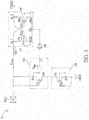
- FIG. 3 is a schematic diagram of an ESD protection circuit 30 according to an embodiment of the present application.
- the ESD protection circuit 30 is similar to the ESD protection circuit 10, and thus, the same components are denoted by the same notations.
- the ESD protection circuit 30 further includes a diode DP.
- the diode DP is coupled between the electrode terminal E2 of the second N-type transistor Q2 and the output terminal Out of the high-voltage tracing circuit TH.
- the diode DP may be utilized to prevent junction breakdown between the N-well NW and the P-well PW (or the deep N-well DNW and the P-well PW) within the second N-type transistor Q2.
- FIG. 4 is a sectional side view of circuit layout regarding the second N-type transistor Q2 and a diode DP4.
- the diode DP4 may be utilized to realize the diode DP in FIG. 3 . As FIG. 4 shows, the diode DP4 may be formed in the P-type substrate PSUB.
- the diode DP4 includes an N-well NW4, an N-type region 400 and a P-type region 402, where the N-type region 400 and the P-type region 402 are formed in the N-well NW4.
- the N-type region 400 is coupled to the output terminal Out of the high-voltage tracing circuit TH
- the P-type region 402 is coupled to the N-type region 227/the electrode terminal E2 of the second N-type transistor Q2.
- the diode DP in FIG. 3 is not limited to be realized by using the diode DP4 in FIG. 4 .
- FIG. 5 is a sectional side view of circuit layout regarding the second N-type transistor Q2 and a diode DP5.
- the diode DP5 may also be utilized to realize the diode DP in FIG. 3 .
- the diode DP5 includes a deep N-well DNW5, a P-well PW5, N-wells NW5, N-type regions 500, 504, 506 and a P-type region 502.
- the P-well PW5 and the N-wells NW5 are both formed on the deep N-well DNW5.
- the N-wells NW5 are disposed by two sides of the P-well PW5.
- the N-type region 500 and the P-type region 502 are formed on the P-well PW5.
- the N-type regions 504 and 506 are formed on the N-well NW5.
- the N-type regions 504, 506 and the P-type region 502 are coupled to the N-type region 227/the electrode terminal E2 of the second N-type transistor Q2.
- the N-type region 500 is coupled to the output terminal Out of the high-voltage tracing circuit TH.
- FIG. 6 is a schematic diagram of an ESD protection circuit 60 according to an embodiment of the present application.
- the ESD protection circuit 60 is similar to the ESD protection circuit 30, and thus, the same components are denoted by the same notations.
- the ESD protection circuit 60 comprises a plurality of diodes DP6.
- the plurality of diodes DP6 are connected in series to form as a diode series, and the diode series is coupled between the electrode terminal E2 of the second N-type transistor Q2 and the output terminal Out of the high-voltage tracing circuit TH, which is also within the scope of the present application.
- FIG. 7 is a schematic diagram of an ESD protection circuit 70 according to an embodiment of the present application.
- the ESD protection circuit 70 is similar to the ESD protection circuit 10, and thus, the same components are denoted by the same notations.
- the high-voltage tracing circuit TH of the ESD protection circuit 70 further includes a diode D1.
- the ESD protection circuit of the present application utilizes the high-voltage tracing circuit to provide the high-voltage tracing voltage larger than the metal pad voltage to the electrode terminal of the second N-type transistor Q2.
- the ESD protection circuit may avoid the leakage current from the P-well to the N-wells.
Landscapes
- Engineering & Computer Science (AREA)
- Microelectronics & Electronic Packaging (AREA)
- Semiconductor Integrated Circuits (AREA)
- Metal-Oxide And Bipolar Metal-Oxide Semiconductor Integrated Circuits (AREA)
Abstract
Description
- The present invention relates to an electrostatic discharge (ESD) protection circuit, and more particularly, to an ESD protection circuit capable of preventing leakage current.
- As electronic technology evolves, electronic devices are applied in a wider area. Electronic devices are not only applied in high technology area such as aerospace equipment, but also applied in consumer electronic products, such as home appliances, communication devices, medical equipment, etc. Electro static discharge (ESD) is everywhere, and ESD problem is a threat for normal operation of equipment. It is an issue of engineer thinking about how to prevent ESD such that the device operates normally. ESD happens usually in real life, especially when the electronic device is manufactured, transported, stored and in usage. When the electrostatic is accumulated to a certain level, energy of a certain degree would be released, which causes irreversible damage on the electronic device.
- The ESD protection circuit in the art has unavoidable leakage current, which increases over all power consumption of the integrated circuit (IC). Therefore, how to prevent leakage current is a significant objective in the field.
- It is therefore a primary objective of embodiments of the present application to provide an ESD protection circuit capable of preventing leakage current.
- To solve the problem stated in the above, the present application provides an ESD protection circuit, including a first N-type transistor including a first gate terminal, coupled to a ground terminal; a first electrode terminal, coupled to the first gate terminal; and a second electrode terminal; a second N-type transistor including a second gate terminal, coupled to a metal pad; a third electrode terminal, coupled to the second gate terminal; a fourth electrode terminal, coupled to the second electrode terminal; and a fifth electrode terminal; and a high-voltage tracing circuit including a first input terminal, coupled to the metal pad, receiving a metal pad voltage; a second input terminal, receiving a supply voltage; and an output terminal, coupled to the fifth electrode terminal, configured to output a high-voltage tracing voltage, wherein the high-voltage tracing voltage is larger than or equal to the metal pad voltage.
- For example, the high-voltage tracing circuit includes a first transistor including a first control terminal, coupled to the second input terminal; a first terminal, coupled to the first input terminal; and a second terminal, coupled to the output terminal; and a second transistor including a second control terminal, coupled to the first input terminal; a third terminal, coupled to the second input terminal; and a fourth terminal, coupled to the output terminal.
- For example, when the metal pad voltage is larger than the supply voltage, the first transistor is conducted and the second transistor is cutoff.
- For example, when the metal pad voltage is less than the supply voltage, the first transistor is cutoff and the second transistor is conducted.
- For example, the high-voltage tracing circuit further includes a diode, coupled between the first input terminal and the first terminal of the first transistor.
- For example, the first N-type transistor further includes a first base terminal, coupled to the first electrode terminal.
- For example, the second N-type transistor includes a first deep N-well, disposed under the third electrode terminal, the fourth electrode terminal and the fifth electrode terminal.
- For example, the second N-type transistor further includes a first P-well, disposed between the third electrode terminal, the fourth electrode terminal and the first deep N-well.
- For example, the second N-type transistor further includes a first N-well, and the first N-well is disposed by a side of the first P-well.
- For example, the N-type region is formed as the fifth electrode terminal.
- For example, when a metal pad voltage of the metal pad is a positive ESD voltage, a first current flows to the ground terminal through the first N-type transistor.
- For example, when a metal pad voltage of the metal pad is a positive ESD voltage, the first N-type transistor is formed as a first bipolar transistor.
- For example, when a metal pad voltage of the metal pad is a negative ESD voltage, a second current flows to the metal pad through the second N-type transistor.
- For example, when a metal pad voltage of the metal pad is a negative ESD voltage, the second N-type transistor is formed as a second bipolar transistor.
- For example, the high-voltage tracing voltage is a maximum voltage of the metal pad voltage and the supply voltage.
- For example, the ESD protection circuit further includes a diode, coupled between the fifth electrode terminal of the second N-type transistor and the output terminal of the high-voltage tracing circuit.
- For example, the diode includes a first terminal, coupled to the fifth electrode terminal of the second N-type transistor; and a second terminal, coupled to the output terminal of the high-voltage tracing circuit.
- For example, the diode includes a second N-well, disposed under the first terminal and the second terminal.
- For example, the diode includes a second P-well, disposed under the first terminal and the second terminal.
- For example, the diode further includes a second deep N-well, disposed under the second P-well.
- For example, the ESD protection circuit further includes a plurality of diodes, formed as a diode series; wherein the diode series is coupled between the fifth electrode terminal of the second N-type transistor and the output terminal of the high-voltage tracing circuit.
- The ESD protection circuit provided by the present application utilizes the high-voltage tracing circuit to avoid the leakage current, and has advantages of small circuit area and low power consumption.
- One or more exemplary embodiments illustrated by the drawings of the corresponding images, which illustrate exemplary embodiments does not constitute a limited, elements the same reference numerals in the figures of the drawings denote like elements having, unless otherwise stated, the accompanying drawings do not constitute a limit thereon.
-
FIG. 1 is a schematic diagram of an electrostatic discharge (ESD) protection circuit according to an embodiment of the present application. -
FIG. 2 is a sectional side view of circuit layout regarding a first N-type transistor and a second N-type transistor within the ESD protection circuit illustrated inFIG. 1 . -
FIG. 3 is a schematic diagram of an ESD protection circuit according to an embodiment of the present application. -
FIG. 4 is a sectional side view of circuit layout regarding a second N-type transistor and a diode within the ESD protection circuit illustrated inFIG. 3 . -
FIG. 5 is a sectional side view of circuit layout regarding the second N-type transistor and a diode within the ESD protection circuit illustrated inFIG. 3 . -
FIG. 6 is a schematic diagram of an ESD protection circuit according to an embodiment of the present application. -
FIG. 7 is a schematic diagram of an ESD protection circuit according to an embodiment of the present application. - In order to make the objects, technical solutions and advantages of the present invention become more apparent, the following relies on the accompanying drawings and embodiments to describe the present invention in further detail. It should be understood that the specific embodiments described herein are only for explaining the present invention and are not intended to limit the present invention.
- Please refer to
FIG. 1 andFIG. 2 .FIG. 1 is a schematic diagram of an electrostatic discharge (ESD)protection circuit 10 according to an embodiment of the present inventionFIG. 2 is a sectional side view of circuit layout regarding a first N-type transistor Q1 and a second N-type transistor Q2. TheESD protection circuit 10 includes the first N-type transistor Q1, the second N-type transistor Q2 and a high-voltage tracing circuit TH. The first N-type transistor Q1 includes a gate terminal G1 and electrode terminals S1 and D1. The second N-type transistor Q2 includes a gate terminal G2 and electrode terminals S2, D2 and E2. The gate terminal G1 and the electrode terminal S1 are coupled to a ground terminal GND. The gate terminal G2 and the electrode terminal S2 are coupled to a metal pad PAD. The electrode terminal D1 of the first N-type transistor Q1 is coupled to the electrode terminal D2 of the second N-type transistor. The high-voltage tracing circuit TH has input terminals In_1 and In_2 and an output terminal Out. The input terminal In_1 is coupled to the metal pad PAD, configured to receive a metal pad voltage VPAD. The input terminal In_2 is configured to receive a supply voltage VDDIO. The output terminal Out is coupled to the electrode terminal E2 of the second N-type transistor Q2, configured to output a high-voltage tracing voltage VE2, wherein the high-voltage tracing voltage VE2 is larger than or equal to the metal pad voltage VPAD. - Specifically, as shown in
FIG. 2 , the first N-type transistor Q1 is formed on a P-type substrate PSUB. That is, the N-type regions type regions type region 200 may be formed as the electrode terminal D1 of the first N-type transistor Q1. The N-type region 202 may be formed as the electrode terminal S1 of the first N-type transistor Q1. An oxide layer and a poly silicon layer, disposed between the N-type region 200 and the N-type region 202, are formed as the gate terminal G1 of the first N-type transistor Q1. In addition, the P-type region 204 may be formed as a base terminal B1 of the first N-type transistor Q1. The gate terminal G1, the electrode terminal S1 and the base terminal B1 of the first N-type transistor Q1 are all coupled to the ground terminal GND. - In addition, the second N-type transistor Q2 includes a deep N-well DNW, a P-well PW, N-wells NW, N-
type regions type regions type regions type regions type regions type region 220 may be formed as the electrode terminal S2 of the second N-type transistor Q2, and the N-type region 222 may be formed as the electrode terminal D2 of the second N-type transistor Q2. An oxide layer and a poly silicon layer, disposed between the N-type region 220 and the N-type region 222, are formed as the gate terminal G2 of the second N-type transistor Q2. In addition, the P-type region 226 may be formed as a base terminal B2 of the second N-type transistor Q2. The gate terminal G2, the electrode terminal S2 and the base terminal B2 of the second N-type transistor Q2 are all coupled to the metal pad PAD. In addition, the N-type regions - Notably, junctions between the P-well PW of the second N-type transistor Q2 and the N-well NW would form parasitic diodes Dpar. When the forward bias between the P-well PW and the N-wells NW is too large, it is equivalent that the parasitic diodes Dpar are conducted, and leakage current from the P-well PW to the N-wells NW is generated.
- To solve the leakage current problem, the high-voltage tracing circuit TH may output the high-voltage tracing voltage VE2 which is larger than or equal to the metal pad voltage VPAD, to prevent the leakage current. Specifically, the high-voltage tracing circuit TH includes a first transistor P1 and a second transistor P2. In an embodiment, the first transistor P1 and the second transistor P2 are all PMOS. A gate PG1 of the first transistor P1 is coupled to the input terminal In_2 to receive the supply voltage VDDIO. A source PS1 of the first transistor P1 is coupled to the input terminal In_1 to receive the metal pad voltage VPAD. A gate PG2 of the second transistor P2 is coupled to the input terminal In_1 to receive the metal pad voltage VPAD. A source PS2 of the second transistor P2 is coupled to the input terminal In_2 to receive the supply voltage VDDIO, a drain PD1 of the first transistor P1 and a drain PD2 of the second transistor P2 are both coupled to the electrode terminal E2 of the second N-type transistor Q2. Ignoring a threshold voltage Vth of the first transistor P1 and the second transistor P2, when the metal pad voltage VPAD is larger than the supply voltage VDDIO, the first transistor P1 is conducted and the second transistor P2 is cutoff. At this time, the high-voltage tracing circuit TH outputs the high-voltage tracing voltage VE2 as the metal pad voltage VPAD to the electrode terminal E2 of the second N-type transistor Q2. On the other hand, when the metal pad voltage VPAD is less than the supply voltage VDDIO, the first transistor P1 is cutoff and the second transistor P2 is conducted. At this time, the high-voltage tracing circuit TH outputs the high-voltage tracing voltage VE2 as the supply voltage VDDIO to the electrode terminal E2 of the second N-type transistor Q2. In other words, the high-voltage tracing voltage VE2 outputted by the high-voltage tracing circuit TH is a maximum voltage of the metal pad voltage VPAD and the supply voltage VDDIO, i.e., VE2 =max (VPAD, VDDIO) . It implies that, the high-voltage tracing voltage VE2 outputted by the high-voltage tracing circuit TH is larger than or equal to the metal pad voltage VPAD. In this case, the junctions between the P-well PW of the second N-type transistor Q2 and the N-wells NW would hardly have sufficient forward bias, or the forward bias is insufficient. The parasitic diodes Dpar are rarely conducted, which solves the leakage current problem between the P-well PW and the N-wells NW.
- In addition, an
internal circuit 12, protected by theESD protection circuit 10, is coupled to the metal pad PAD, where the metal pad PAD, theESD protection circuit 10 and theinternal circuit 12 may be integrated in an integrated circuit (IC) . Under a normal operation condition, i.e., when a voltage difference between the metal pad PAD and the ground terminal GND is substantially the supply voltage VDDIO of the IC, a loop from the metal pad PAD to the ground terminal GND is cutoff. When an extremely high voltage exists between the metal pad PAD and the ground terminal GND, e.g., ESD Zap, or during ESD testing, a current path within theESD protection circuit 10 from the metal pad PAD to the ground terminal GND may be formed, which means that the loop from the metal pad PAD to the ground terminal GND is conducted, so as to prevent the extremely high voltage and its current has impact on theinternal circuit 12, e.g., damages theinternal circuit 12. - Specifically, under a normal operation condition, when the metal pad voltage VPAD of the metal pad PAD is substantially the supply voltage VDDIO, the second N-type transistor Q2 is conducted and the first N-type transistor Q1 is cutoff. When the metal pad voltage VPAD is substantially negative of the supply voltage, i.e., -VDDIO, the second N-type transistor Q2 is cutoff and the first N-type transistor Q1 is conducted. In other words, under the normal operation condition, the loop between the metal pad PAD and the ground terminal GND is cutoff.
- On the other hand, when ESD Zap occurs or it is during ESD testing, the first N-type transistor Q1 (or the second N-type transistor Q2) is equivalent to a bipolar transistor and the current path is formed, which is to prevent the
internal circuit 12 from being damaged. Specifically, when the metal pad voltage VPAD receives a positive ESD voltage, e.g., VPAD=2 kilovolt (KV), the second N-type transistor Q2 is conducted, and the P-type substrate PSUB of the first N-type transistor Q1 and the N-type regions type regions internal circuit 12 and damaging theinternal circuit 12. - As can be seen, the
ESD protection circuit 10 utilizes the high-voltage tracing circuit TH to provide the high-voltage tracing voltage VE2 which is larger than the metal pad voltage VPAD to the electrode terminal E2 of the second N-type transistor Q2. Hence, theESD protection circuit 10 would not have the leakage current flowing from the P-well PW to the N-well NW. - Notably, the embodiments stated in the above are utilized for illustrating the concept of the present application. Those skilled in the art may make modifications and alterations accordingly, and not limited herein. For example, please refer to
FIG. 3 , which is a schematic diagram of anESD protection circuit 30 according to an embodiment of the present application. TheESD protection circuit 30 is similar to theESD protection circuit 10, and thus, the same components are denoted by the same notations. Different from theESD protection circuit 10, theESD protection circuit 30 further includes a diode DP. The diode DP is coupled between the electrode terminal E2 of the second N-type transistor Q2 and the output terminal Out of the high-voltage tracing circuit TH. When the metal pad voltage VPAD is negative, the diode DP may be utilized to prevent junction breakdown between the N-well NW and the P-well PW (or the deep N-well DNW and the P-well PW) within the second N-type transistor Q2. Please refer toFIG. 4 to see the detail connection between the second N-type transistor Q2 and the diode DP.FIG. 4 is a sectional side view of circuit layout regarding the second N-type transistor Q2 and a diode DP4. The diode DP4 may be utilized to realize the diode DP inFIG. 3 . AsFIG. 4 shows, the diode DP4 may be formed in the P-type substrate PSUB. The diode DP4 includes an N-well NW4, an N-type region 400 and a P-type region 402, where the N-type region 400 and the P-type region 402 are formed in the N-well NW4. The N-type region 400 is coupled to the output terminal Out of the high-voltage tracing circuit TH, and the P-type region 402 is coupled to the N-type region 227/the electrode terminal E2 of the second N-type transistor Q2. In addition, the diode DP inFIG. 3 is not limited to be realized by using the diode DP4 inFIG. 4 . For example, please refer toFIG. 5 , which is a sectional side view of circuit layout regarding the second N-type transistor Q2 and a diode DP5. The diode DP5 may also be utilized to realize the diode DP inFIG. 3 . Different from the diode DP4, the diode DP5 includes a deep N-well DNW5, a P-well PW5, N-wells NW5, N-type regions type region 502. The P-well PW5 and the N-wells NW5 are both formed on the deep N-well DNW5. The N-wells NW5 are disposed by two sides of the P-well PW5. In addition, the N-type region 500 and the P-type region 502 are formed on the P-well PW5. The N-type regions type regions type region 502 are coupled to the N-type region 227/the electrode terminal E2 of the second N-type transistor Q2. The N-type region 500 is coupled to the output terminal Out of the high-voltage tracing circuit TH. - In addition, please refer to
FIG. 6 , which is a schematic diagram of anESD protection circuit 60 according to an embodiment of the present application. TheESD protection circuit 60 is similar to theESD protection circuit 30, and thus, the same components are denoted by the same notations. Different from theESD protection circuit 30, theESD protection circuit 60 comprises a plurality of diodes DP6. The plurality of diodes DP6 are connected in series to form as a diode series, and the diode series is coupled between the electrode terminal E2 of the second N-type transistor Q2 and the output terminal Out of the high-voltage tracing circuit TH, which is also within the scope of the present application. - In addition, please refer to
FIG. 7 , which is a schematic diagram of anESD protection circuit 70 according to an embodiment of the present application. TheESD protection circuit 70 is similar to theESD protection circuit 10, and thus, the same components are denoted by the same notations. Different from theESD protection circuit 10, the high-voltage tracing circuit TH of theESD protection circuit 70 further includes a diode D1. The diode D1 is configured to protect the first transistor P1, so as to prevent the first transistor P1 from damage caused by excessive voltage, especially when the metal pad voltage VPAD is negative of the supply voltage VDDIO, i.e., VPAD= -VDDIO. - In summary, the ESD protection circuit of the present application utilizes the high-voltage tracing circuit to provide the high-voltage tracing voltage larger than the metal pad voltage to the electrode terminal of the second N-type transistor Q2. Thus, the ESD protection circuit may avoid the leakage current from the P-well to the N-wells.
- The foregoing is only embodiments of the present application it is preferred not intended to limit the present application, those skilled in the art, the present application may have various changes and variations. Any modification within the spirit and principle of the present application, equivalent substitutions, improvements should be included within the scope of the present invention.
Claims (24)
- An electrostatic discharge (ESD) protection circuit, comprising:a first N-type transistor, comprising:a first gate terminal, coupled to a ground terminal;a first electrode terminal, coupled to the first gate terminal; anda second electrode terminal;a second N-type transistor, comprising:a second gate terminal, coupled to a metal pad;a third electrode terminal, coupled to the second gate terminal;a fourth electrode terminal, coupled to the second electrode terminal; anda fifth electrode terminal; anda high-voltage tracing circuit, comprising:a first input terminal, coupled to the metal pad and configured to receive a metal pad voltage;a second input terminal, configured to receive a supply voltage; andan output terminal, coupled to the fifth electrode terminal, configured to output a high-voltage tracing voltage, wherein the high-voltage tracing voltage is larger than or equal to the metal pad voltage.
- The ESD protection circuit as claim 1, wherein the high-voltage tracing circuit comprises:
a first transistor, comprising:a first control terminal, coupled to the second input terminal;a first terminal, coupled to the first input terminal; anda second terminal, coupled to the output terminal; and a second transistor, comprising:a second control terminal, coupled to the first input terminal;a third terminal, coupled to the second input terminal; anda fourth terminal, coupled to the output terminal. - The ESD protection circuit as claim 2, wherein when the metal pad voltage is larger than the supply voltage, the first transistor is conducted and the second transistor is cutoff.
- The ESD protection circuit as claim 2, wherein when the metal pad voltage is less than the supply voltage, the first transistor is cutoff and the second transistor is conducted.
- The ESD protection circuit as claim 2, wherein the high-voltage tracing circuit further comprises:
a diode, coupled between the first input terminal and the first terminal of the first transistor. - The ESD protection circuit as claim 1, wherein the first N-type transistor further comprises:
a first base terminal, coupled to the first electrode terminal. - The ESD protection circuit as claim 1, wherein the second N-type transistor comprises:
a first deep N-well, disposed under the third electrode terminal, the fourth electrode terminal and the fifth electrode terminal. - The ESD protection circuit as claim 7, wherein the second N-type transistor further comprises a first P-well, disposed between the third electrode terminal, the fourth electrode terminal and the first deep N-well.
- The ESD protection circuit as claim 8, wherein the second N-type transistor further comprises a first N-well, and the first N-well is disposed by a side of the first P-well.
- The ESD protection circuit as claim 9, wherein the second N-type transistor further comprises an N-type region, the N-type region is disposed in the first N-well.
- The ESD protection circuit as claim 10, wherein the N-type region is formed as the fifth electrode terminal.
- The ESD protection circuit as claim 1, wherein when a metal pad voltage of the metal pad is a positive ESD voltage, a first current flows to the ground terminal through the first N-type transistor.
- The ESD protection circuit as claim 1, wherein when a metal pad voltage of the metal pad is a positive ESD voltage, the first N-type transistor is formed as a first bipolar transistor.
- The ESD protection circuit as claim 12 or claim 13, wherein the positive ESD voltage is larger than 1 kilovolt (KV).
- The ESD protection circuit as claim 1, wherein when a metal pad voltage of the metal pad is a negative ESD voltage, a second current flows to the metal pad through the second N-type transistor.
- The ESD protection circuit as claim 1, wherein when a metal pad voltage of the metal pad is a negative ESD voltage, the second N-type transistor is formed as a second bipolar transistor.
- The ESD protection circuit as claim 15 or claim 16, wherein the negative ESD voltage is less than negative 1 kilovolt (KV).
- The ESD protection circuit as claim 1, wherein the high-voltage tracing voltage is a maximum voltage of the metal pad voltage and the supply voltage.
- The ESD protection circuit as claim 1, further comprising:
a diode, coupled between the fifth electrode terminal of the second N-type transistor and the output terminal of the high-voltage tracing circuit. - The ESD protection circuit as claim 19, wherein the diode comprises:a first terminal, coupled to the fifth electrode terminal of the second N-type transistor; anda second terminal, coupled to the output terminal of the high-voltage tracing circuit.
- The ESD protection circuit as claim 20, wherein the diode comprises:
a second N-well, disposed under the first terminal and the second terminal. - The ESD protection circuit as claim 20, wherein the diode comprises:
a second P-well, disposed under the first terminal and the second terminal. - The ESD protection circuit as claim 22, wherein the diode further comprises:
a second deep N-well, disposed under the second P-well. - The ESD protection circuit of any as claims 1-23, further comprising:a plurality of diodes, formed as a diode series;wherein the diode series is coupled between the fifth electrode terminal of the second N-type transistor and the output terminal of the high-voltage tracing circuit.
Applications Claiming Priority (2)
| Application Number | Priority Date | Filing Date | Title |
|---|---|---|---|
| CN2016100109 | 2016-09-26 | ||
| PCT/CN2017/074450 WO2018053991A1 (en) | 2016-09-26 | 2017-02-22 | Electrostatic-discharge protection circuit applied to integrated circuit |
Publications (3)
| Publication Number | Publication Date |
|---|---|
| EP3324439A1 true EP3324439A1 (en) | 2018-05-23 |
| EP3324439A4 EP3324439A4 (en) | 2018-09-12 |
| EP3324439B1 EP3324439B1 (en) | 2020-09-02 |
Family
ID=61690122
Family Applications (1)
| Application Number | Title | Priority Date | Filing Date |
|---|---|---|---|
| EP17794646.4A Active EP3324439B1 (en) | 2016-09-26 | 2017-02-22 | Electrostatic-discharge protection circuit applied to integrated circuit |
Country Status (5)
| Country | Link |
|---|---|
| US (1) | US10134725B2 (en) |
| EP (1) | EP3324439B1 (en) |
| KR (1) | KR102001899B1 (en) |
| CN (1) | CN109478549B (en) |
| WO (1) | WO2018053991A1 (en) |
Families Citing this family (10)
| Publication number | Priority date | Publication date | Assignee | Title |
|---|---|---|---|---|
| US10147716B2 (en) | 2016-03-31 | 2018-12-04 | Macronix International Co., Ltd. | Electrostatic discharge protection apparatus and applications thereof |
| US10304820B1 (en) * | 2018-03-30 | 2019-05-28 | Macronix International Co., Ltd. | Electrostatic discharge protection apparatus and applications thereof |
| TWI710096B (en) * | 2019-09-04 | 2020-11-11 | 智原科技股份有限公司 | Electrostatic discharge protection apparatus |
| US11689014B2 (en) | 2021-06-24 | 2023-06-27 | Qualcomm Incorporated | Electrostatic discharge circuit for multi-voltage rail thin-gate output driver |
| CN113471193B (en) * | 2021-06-28 | 2024-07-09 | 深圳砺芯半导体有限责任公司 | Anti-latch-up composite device for ESD protection of positive and negative power supplies |
| US12382658B2 (en) * | 2021-07-01 | 2025-08-05 | Texas Instruments Incorporated | Reducing transistor breakdown in a power FET current sense stack |
| US11575259B2 (en) | 2021-07-08 | 2023-02-07 | Qualcomm Incorporated | Interface circuit with robust electrostatic discharge |
| TWI764813B (en) * | 2021-08-18 | 2022-05-11 | 立積電子股份有限公司 | Driving circuit |
| WO2024220964A1 (en) * | 2023-04-20 | 2024-10-24 | Microchip Technology Incorporated | Device and system for esd protection |
| US12446324B2 (en) * | 2023-04-20 | 2025-10-14 | Microchip Technology Incorporated | Device and system for ESD protection |
Family Cites Families (21)
| Publication number | Priority date | Publication date | Assignee | Title |
|---|---|---|---|---|
| JPH07226486A (en) * | 1994-02-15 | 1995-08-22 | Nissan Motor Co Ltd | Semiconductor device protection circuit |
| US6399990B1 (en) * | 2000-03-21 | 2002-06-04 | International Business Machines Corporation | Isolated well ESD device |
| US6747861B2 (en) * | 2001-11-15 | 2004-06-08 | Industrial Technology Research Institute | Electrostatic discharge protection for a mixed-voltage device using a stacked-transistor-triggered silicon controlled rectifier |
| US7064942B2 (en) * | 2003-05-19 | 2006-06-20 | Silicon Integrated Systems Corp. | ESD protection circuit with tunable gate-bias |
| US7167350B2 (en) * | 2003-11-14 | 2007-01-23 | Texas Instruments Incorporated | Design implementation to suppress latchup in voltage tolerant circuits |
| CN1649142A (en) * | 2004-01-19 | 2005-08-03 | 财团法人工业技术研究院 | Electrostatic discharge protection circuit and electrostatic discharge protection method |
| US20060065932A1 (en) * | 2004-09-30 | 2006-03-30 | Taiwan Semiconductor Manufacturing Co., Ltd. | Circuit to improve ESD performance made by fully silicided process |
| CN100382313C (en) * | 2005-12-07 | 2008-04-16 | 威盛电子股份有限公司 | Electrostatic discharge protection circuit |
| KR100723519B1 (en) * | 2006-01-06 | 2007-05-30 | 삼성전자주식회사 | Voltage clamping circuit using MOOS transistor and semiconductor chip having same |
| US7397280B2 (en) * | 2006-03-02 | 2008-07-08 | Industrial Technology Research Institute | High-voltage tolerant power-rail ESD clamp circuit for mixed-voltage I/O interface |
| TW200739872A (en) * | 2006-04-04 | 2007-10-16 | Univ Nat Chiao Tung | Power line electrostatic discharge protection circuit featuring triple voltage tolerance |
| KR100725103B1 (en) * | 2006-05-22 | 2007-06-04 | 삼성전자주식회사 | Electrostatic discharge circuit and method for reducing input capacitance of semiconductor chip having same |
| CN100525000C (en) * | 2006-11-24 | 2009-08-05 | 上海华虹Nec电子有限公司 | Static discharge protection circuit and structure for part charging mode |
| US7719805B2 (en) * | 2006-12-01 | 2010-05-18 | Macronix International Co., Ltd. | ESD protection circuit |
| JP2009087962A (en) * | 2007-09-27 | 2009-04-23 | Panasonic Corp | Protection circuit and semiconductor integrated circuit |
| JP2009130119A (en) * | 2007-11-22 | 2009-06-11 | Toshiba Corp | Semiconductor integrated circuit |
| JP2009218296A (en) * | 2008-03-07 | 2009-09-24 | Rohm Co Ltd | Protection circuit |
| US8102002B2 (en) * | 2008-12-16 | 2012-01-24 | Analog Devices, Inc. | System and method for isolated NMOS-based ESD clamp cell |
| US8134813B2 (en) * | 2009-01-29 | 2012-03-13 | Xilinx, Inc. | Method and apparatus to reduce footprint of ESD protection within an integrated circuit |
| US8427796B2 (en) * | 2010-01-19 | 2013-04-23 | Qualcomm, Incorporated | High voltage, high frequency ESD protection circuit for RF ICs |
| US20130099297A1 (en) * | 2011-10-20 | 2013-04-25 | Macronix International Co., Ltd. | Electrostatic discharge protection device |
-
2017
- 2017-02-22 CN CN201780000117.1A patent/CN109478549B/en active Active
- 2017-02-22 KR KR1020177034725A patent/KR102001899B1/en active Active
- 2017-02-22 EP EP17794646.4A patent/EP3324439B1/en active Active
- 2017-02-22 WO PCT/CN2017/074450 patent/WO2018053991A1/en not_active Ceased
- 2017-11-15 US US15/813,179 patent/US10134725B2/en active Active
Also Published As
| Publication number | Publication date |
|---|---|
| CN109478549A (en) | 2019-03-15 |
| KR102001899B1 (en) | 2019-10-21 |
| EP3324439A4 (en) | 2018-09-12 |
| US10134725B2 (en) | 2018-11-20 |
| US20180090482A1 (en) | 2018-03-29 |
| KR20180044850A (en) | 2018-05-03 |
| WO2018053991A1 (en) | 2018-03-29 |
| EP3324439B1 (en) | 2020-09-02 |
| CN109478549B (en) | 2021-05-11 |
Similar Documents
| Publication | Publication Date | Title |
|---|---|---|
| US10134725B2 (en) | Electrostatic discharge protection circuit applied in integrated circuit | |
| KR101870995B1 (en) | Esd protection circuit of semiconductor integrated circuit | |
| JP5540801B2 (en) | ESD protection circuit and semiconductor device | |
| US9076654B2 (en) | Semiconductor device | |
| EP3404713B1 (en) | Electrostatic discharge (esd) protection device and method for operating an esd protection device | |
| US7394631B2 (en) | Electrostatic protection circuit | |
| US10063048B2 (en) | Dynamic trigger voltage control for an ESD protection device | |
| US9812437B2 (en) | Semiconductor integrated circuit device, and electronic appliance using the same | |
| US9437590B2 (en) | Electrostatic discharge protection device and electrostatic discharge protection system | |
| US7763908B2 (en) | Design of silicon-controlled rectifier by considering electrostatic discharge robustness in human-body model and charged-device model devices | |
| EP3503184A1 (en) | Device and method for electrostatic discharge (esd) protection | |
| TW202107793A (en) | High voltage circuitry device and its ring circuitry layout | |
| EP3367436A1 (en) | Electrostatic discharge (esd) protection device and method for operating an esd protection device | |
| US10290628B2 (en) | Electrostatic discharge protection circuit | |
| US7746611B2 (en) | ESD protective circuit having low leakage current | |
| US8823129B2 (en) | Latch-up prevention structure and method for ultra-small high voltage tolerant cell | |
| US7929264B2 (en) | Electro-static discharge protection device having a low trigger voltage and reduced size | |
| CN109983576B (en) | Electrostatic discharge protection device | |
| CN211743125U (en) | Transition voltage protection device | |
| KR100557643B1 (en) | RS protective circuit | |
| CN113471193B (en) | Anti-latch-up composite device for ESD protection of positive and negative power supplies | |
| KR20160046552A (en) | Esd protection circuit | |
| JP2010177545A (en) | Esd protection circuit |
Legal Events
| Date | Code | Title | Description |
|---|---|---|---|
| STAA | Information on the status of an ep patent application or granted ep patent |
Free format text: STATUS: UNKNOWN |
|
| STAA | Information on the status of an ep patent application or granted ep patent |
Free format text: STATUS: THE INTERNATIONAL PUBLICATION HAS BEEN MADE |
|
| PUAI | Public reference made under article 153(3) epc to a published international application that has entered the european phase |
Free format text: ORIGINAL CODE: 0009012 |
|
| STAA | Information on the status of an ep patent application or granted ep patent |
Free format text: STATUS: REQUEST FOR EXAMINATION WAS MADE |
|
| 17P | Request for examination filed |
Effective date: 20171116 |
|
| AK | Designated contracting states |
Kind code of ref document: A1 Designated state(s): AL AT BE BG CH CY CZ DE DK EE ES FI FR GB GR HR HU IE IS IT LI LT LU LV MC MK MT NL NO PL PT RO RS SE SI SK SM TR |
|
| AX | Request for extension of the european patent |
Extension state: BA ME |
|
| A4 | Supplementary search report drawn up and despatched |
Effective date: 20180810 |
|
| RIC1 | Information provided on ipc code assigned before grant |
Ipc: H02H 9/04 20060101ALI20180806BHEP Ipc: H01L 27/02 20060101AFI20180806BHEP |
|
| DAV | Request for validation of the european patent (deleted) | ||
| DAX | Request for extension of the european patent (deleted) | ||
| GRAP | Despatch of communication of intention to grant a patent |
Free format text: ORIGINAL CODE: EPIDOSNIGR1 |
|
| STAA | Information on the status of an ep patent application or granted ep patent |
Free format text: STATUS: GRANT OF PATENT IS INTENDED |
|
| INTG | Intention to grant announced |
Effective date: 20200408 |
|
| RIC1 | Information provided on ipc code assigned before grant |
Ipc: H02H 9/04 20060101ALI20200327BHEP Ipc: H01L 27/02 20060101AFI20200327BHEP |
|
| GRAS | Grant fee paid |
Free format text: ORIGINAL CODE: EPIDOSNIGR3 |
|
| GRAA | (expected) grant |
Free format text: ORIGINAL CODE: 0009210 |
|
| STAA | Information on the status of an ep patent application or granted ep patent |
Free format text: STATUS: THE PATENT HAS BEEN GRANTED |
|
| AK | Designated contracting states |
Kind code of ref document: B1 Designated state(s): AL AT BE BG CH CY CZ DE DK EE ES FI FR GB GR HR HU IE IS IT LI LT LU LV MC MK MT NL NO PL PT RO RS SE SI SK SM TR |
|
| REG | Reference to a national code |
Ref country code: GB Ref legal event code: FG4D |
|
| REG | Reference to a national code |
Ref country code: AT Ref legal event code: REF Ref document number: 1309816 Country of ref document: AT Kind code of ref document: T Effective date: 20200915 Ref country code: CH Ref legal event code: EP |
|
| REG | Reference to a national code |
Ref country code: DE Ref legal event code: R096 Ref document number: 602017022962 Country of ref document: DE |
|
| REG | Reference to a national code |
Ref country code: IE Ref legal event code: FG4D |
|
| REG | Reference to a national code |
Ref country code: LT Ref legal event code: MG4D |
|
| PG25 | Lapsed in a contracting state [announced via postgrant information from national office to epo] |
Ref country code: SE Free format text: LAPSE BECAUSE OF FAILURE TO SUBMIT A TRANSLATION OF THE DESCRIPTION OR TO PAY THE FEE WITHIN THE PRESCRIBED TIME-LIMIT Effective date: 20200902 Ref country code: GR Free format text: LAPSE BECAUSE OF FAILURE TO SUBMIT A TRANSLATION OF THE DESCRIPTION OR TO PAY THE FEE WITHIN THE PRESCRIBED TIME-LIMIT Effective date: 20201203 Ref country code: FI Free format text: LAPSE BECAUSE OF FAILURE TO SUBMIT A TRANSLATION OF THE DESCRIPTION OR TO PAY THE FEE WITHIN THE PRESCRIBED TIME-LIMIT Effective date: 20200902 Ref country code: BG Free format text: LAPSE BECAUSE OF FAILURE TO SUBMIT A TRANSLATION OF THE DESCRIPTION OR TO PAY THE FEE WITHIN THE PRESCRIBED TIME-LIMIT Effective date: 20201202 Ref country code: NO Free format text: LAPSE BECAUSE OF FAILURE TO SUBMIT A TRANSLATION OF THE DESCRIPTION OR TO PAY THE FEE WITHIN THE PRESCRIBED TIME-LIMIT Effective date: 20201202 Ref country code: LT Free format text: LAPSE BECAUSE OF FAILURE TO SUBMIT A TRANSLATION OF THE DESCRIPTION OR TO PAY THE FEE WITHIN THE PRESCRIBED TIME-LIMIT Effective date: 20200902 Ref country code: HR Free format text: LAPSE BECAUSE OF FAILURE TO SUBMIT A TRANSLATION OF THE DESCRIPTION OR TO PAY THE FEE WITHIN THE PRESCRIBED TIME-LIMIT Effective date: 20200902 |
|
| REG | Reference to a national code |
Ref country code: NL Ref legal event code: MP Effective date: 20200902 |
|
| REG | Reference to a national code |
Ref country code: AT Ref legal event code: MK05 Ref document number: 1309816 Country of ref document: AT Kind code of ref document: T Effective date: 20200902 |
|
| PG25 | Lapsed in a contracting state [announced via postgrant information from national office to epo] |
Ref country code: RS Free format text: LAPSE BECAUSE OF FAILURE TO SUBMIT A TRANSLATION OF THE DESCRIPTION OR TO PAY THE FEE WITHIN THE PRESCRIBED TIME-LIMIT Effective date: 20200902 Ref country code: PL Free format text: LAPSE BECAUSE OF FAILURE TO SUBMIT A TRANSLATION OF THE DESCRIPTION OR TO PAY THE FEE WITHIN THE PRESCRIBED TIME-LIMIT Effective date: 20200902 Ref country code: LV Free format text: LAPSE BECAUSE OF FAILURE TO SUBMIT A TRANSLATION OF THE DESCRIPTION OR TO PAY THE FEE WITHIN THE PRESCRIBED TIME-LIMIT Effective date: 20200902 |
|
| PG25 | Lapsed in a contracting state [announced via postgrant information from national office to epo] |
Ref country code: SM Free format text: LAPSE BECAUSE OF FAILURE TO SUBMIT A TRANSLATION OF THE DESCRIPTION OR TO PAY THE FEE WITHIN THE PRESCRIBED TIME-LIMIT Effective date: 20200902 Ref country code: PT Free format text: LAPSE BECAUSE OF FAILURE TO SUBMIT A TRANSLATION OF THE DESCRIPTION OR TO PAY THE FEE WITHIN THE PRESCRIBED TIME-LIMIT Effective date: 20210104 Ref country code: RO Free format text: LAPSE BECAUSE OF FAILURE TO SUBMIT A TRANSLATION OF THE DESCRIPTION OR TO PAY THE FEE WITHIN THE PRESCRIBED TIME-LIMIT Effective date: 20200902 Ref country code: CZ Free format text: LAPSE BECAUSE OF FAILURE TO SUBMIT A TRANSLATION OF THE DESCRIPTION OR TO PAY THE FEE WITHIN THE PRESCRIBED TIME-LIMIT Effective date: 20200902 Ref country code: EE Free format text: LAPSE BECAUSE OF FAILURE TO SUBMIT A TRANSLATION OF THE DESCRIPTION OR TO PAY THE FEE WITHIN THE PRESCRIBED TIME-LIMIT Effective date: 20200902 |
|
| PG25 | Lapsed in a contracting state [announced via postgrant information from national office to epo] |
Ref country code: IS Free format text: LAPSE BECAUSE OF FAILURE TO SUBMIT A TRANSLATION OF THE DESCRIPTION OR TO PAY THE FEE WITHIN THE PRESCRIBED TIME-LIMIT Effective date: 20210102 Ref country code: AL Free format text: LAPSE BECAUSE OF FAILURE TO SUBMIT A TRANSLATION OF THE DESCRIPTION OR TO PAY THE FEE WITHIN THE PRESCRIBED TIME-LIMIT Effective date: 20200902 Ref country code: AT Free format text: LAPSE BECAUSE OF FAILURE TO SUBMIT A TRANSLATION OF THE DESCRIPTION OR TO PAY THE FEE WITHIN THE PRESCRIBED TIME-LIMIT Effective date: 20200902 Ref country code: ES Free format text: LAPSE BECAUSE OF FAILURE TO SUBMIT A TRANSLATION OF THE DESCRIPTION OR TO PAY THE FEE WITHIN THE PRESCRIBED TIME-LIMIT Effective date: 20200902 |
|
| REG | Reference to a national code |
Ref country code: DE Ref legal event code: R097 Ref document number: 602017022962 Country of ref document: DE |
|
| PG25 | Lapsed in a contracting state [announced via postgrant information from national office to epo] |
Ref country code: SK Free format text: LAPSE BECAUSE OF FAILURE TO SUBMIT A TRANSLATION OF THE DESCRIPTION OR TO PAY THE FEE WITHIN THE PRESCRIBED TIME-LIMIT Effective date: 20200902 |
|
| PLBE | No opposition filed within time limit |
Free format text: ORIGINAL CODE: 0009261 |
|
| STAA | Information on the status of an ep patent application or granted ep patent |
Free format text: STATUS: NO OPPOSITION FILED WITHIN TIME LIMIT |
|
| 26N | No opposition filed |
Effective date: 20210603 |
|
| PG25 | Lapsed in a contracting state [announced via postgrant information from national office to epo] |
Ref country code: SI Free format text: LAPSE BECAUSE OF FAILURE TO SUBMIT A TRANSLATION OF THE DESCRIPTION OR TO PAY THE FEE WITHIN THE PRESCRIBED TIME-LIMIT Effective date: 20200902 Ref country code: DK Free format text: LAPSE BECAUSE OF FAILURE TO SUBMIT A TRANSLATION OF THE DESCRIPTION OR TO PAY THE FEE WITHIN THE PRESCRIBED TIME-LIMIT Effective date: 20200902 |
|
| PG25 | Lapsed in a contracting state [announced via postgrant information from national office to epo] |
Ref country code: MC Free format text: LAPSE BECAUSE OF FAILURE TO SUBMIT A TRANSLATION OF THE DESCRIPTION OR TO PAY THE FEE WITHIN THE PRESCRIBED TIME-LIMIT Effective date: 20200902 |
|
| REG | Reference to a national code |
Ref country code: BE Ref legal event code: MM Effective date: 20210228 |
|
| PG25 | Lapsed in a contracting state [announced via postgrant information from national office to epo] |
Ref country code: LU Free format text: LAPSE BECAUSE OF NON-PAYMENT OF DUE FEES Effective date: 20210222 Ref country code: IT Free format text: LAPSE BECAUSE OF FAILURE TO SUBMIT A TRANSLATION OF THE DESCRIPTION OR TO PAY THE FEE WITHIN THE PRESCRIBED TIME-LIMIT Effective date: 20200902 Ref country code: LI Free format text: LAPSE BECAUSE OF NON-PAYMENT OF DUE FEES Effective date: 20210228 Ref country code: CH Free format text: LAPSE BECAUSE OF NON-PAYMENT OF DUE FEES Effective date: 20210228 |
|
| PG25 | Lapsed in a contracting state [announced via postgrant information from national office to epo] |
Ref country code: IE Free format text: LAPSE BECAUSE OF NON-PAYMENT OF DUE FEES Effective date: 20210222 Ref country code: FR Free format text: LAPSE BECAUSE OF NON-PAYMENT OF DUE FEES Effective date: 20210228 |
|
| PG25 | Lapsed in a contracting state [announced via postgrant information from national office to epo] |
Ref country code: BE Free format text: LAPSE BECAUSE OF NON-PAYMENT OF DUE FEES Effective date: 20210228 |
|
| PG25 | Lapsed in a contracting state [announced via postgrant information from national office to epo] |
Ref country code: NL Free format text: LAPSE BECAUSE OF NON-PAYMENT OF DUE FEES Effective date: 20200923 Ref country code: CY Free format text: LAPSE BECAUSE OF FAILURE TO SUBMIT A TRANSLATION OF THE DESCRIPTION OR TO PAY THE FEE WITHIN THE PRESCRIBED TIME-LIMIT Effective date: 20200902 |
|
| PG25 | Lapsed in a contracting state [announced via postgrant information from national office to epo] |
Ref country code: HU Free format text: LAPSE BECAUSE OF FAILURE TO SUBMIT A TRANSLATION OF THE DESCRIPTION OR TO PAY THE FEE WITHIN THE PRESCRIBED TIME-LIMIT; INVALID AB INITIO Effective date: 20170222 |
|
| PG25 | Lapsed in a contracting state [announced via postgrant information from national office to epo] |
Ref country code: MK Free format text: LAPSE BECAUSE OF FAILURE TO SUBMIT A TRANSLATION OF THE DESCRIPTION OR TO PAY THE FEE WITHIN THE PRESCRIBED TIME-LIMIT Effective date: 20200902 |
|
| REG | Reference to a national code |
Ref country code: DE Ref legal event code: R082 Ref document number: 602017022962 Country of ref document: DE Representative=s name: STRAUS, ALEXANDER, DIPL.-CHEM.UNIV. DR.PHIL., DE |
|
| PG25 | Lapsed in a contracting state [announced via postgrant information from national office to epo] |
Ref country code: MT Free format text: LAPSE BECAUSE OF FAILURE TO SUBMIT A TRANSLATION OF THE DESCRIPTION OR TO PAY THE FEE WITHIN THE PRESCRIBED TIME-LIMIT Effective date: 20200902 |
|
| REG | Reference to a national code |
Ref country code: DE Ref legal event code: R079 Ref document number: 602017022962 Country of ref document: DE Free format text: PREVIOUS MAIN CLASS: H01L0027020000 Ipc: H10D0089000000 |
|
| PG25 | Lapsed in a contracting state [announced via postgrant information from national office to epo] |
Ref country code: TR Free format text: LAPSE BECAUSE OF FAILURE TO SUBMIT A TRANSLATION OF THE DESCRIPTION OR TO PAY THE FEE WITHIN THE PRESCRIBED TIME-LIMIT Effective date: 20200902 |
|
| PGFP | Annual fee paid to national office [announced via postgrant information from national office to epo] |
Ref country code: GB Payment date: 20260216 Year of fee payment: 10 |
|
| PGFP | Annual fee paid to national office [announced via postgrant information from national office to epo] |
Ref country code: DE Payment date: 20260211 Year of fee payment: 10 |