EP3320618B1 - Filter circuit for filtering an input signal of an analogue-to-digital converter - Google Patents
Filter circuit for filtering an input signal of an analogue-to-digital converter Download PDFInfo
- Publication number
- EP3320618B1 EP3320618B1 EP16742192.4A EP16742192A EP3320618B1 EP 3320618 B1 EP3320618 B1 EP 3320618B1 EP 16742192 A EP16742192 A EP 16742192A EP 3320618 B1 EP3320618 B1 EP 3320618B1
- Authority
- EP
- European Patent Office
- Prior art keywords
- signal
- circuit
- input
- filter
- input signal
- Prior art date
- Legal status (The legal status is an assumption and is not a legal conclusion. Google has not performed a legal analysis and makes no representation as to the accuracy of the status listed.)
- Active
Links
- 238000001914 filtration Methods 0.000 title claims description 9
- 230000010354 integration Effects 0.000 claims description 72
- 239000003990 capacitor Substances 0.000 claims description 16
- 238000000034 method Methods 0.000 claims description 11
- 230000008569 process Effects 0.000 claims description 2
- 230000009466 transformation Effects 0.000 claims 2
- 238000010586 diagram Methods 0.000 description 11
- 230000000737 periodic effect Effects 0.000 description 4
- 230000008901 benefit Effects 0.000 description 2
- 238000006243 chemical reaction Methods 0.000 description 2
- 230000001419 dependent effect Effects 0.000 description 2
- 238000005070 sampling Methods 0.000 description 2
- 230000001174 ascending effect Effects 0.000 description 1
- 230000008878 coupling Effects 0.000 description 1
- 238000010168 coupling process Methods 0.000 description 1
- 238000005859 coupling reaction Methods 0.000 description 1
- 230000004069 differentiation Effects 0.000 description 1
- 238000013507 mapping Methods 0.000 description 1
- 230000003071 parasitic effect Effects 0.000 description 1
- 230000003252 repetitive effect Effects 0.000 description 1
- 230000004044 response Effects 0.000 description 1
Images


Classifications
-
- H—ELECTRICITY
- H03—ELECTRONIC CIRCUITRY
- H03M—CODING; DECODING; CODE CONVERSION IN GENERAL
- H03M1/00—Analogue/digital conversion; Digital/analogue conversion
- H03M1/06—Continuously compensating for, or preventing, undesired influence of physical parameters
- H03M1/08—Continuously compensating for, or preventing, undesired influence of physical parameters of noise
- H03M1/0863—Continuously compensating for, or preventing, undesired influence of physical parameters of noise of switching transients, e.g. glitches
-
- H—ELECTRICITY
- H03—ELECTRONIC CIRCUITRY
- H03M—CODING; DECODING; CODE CONVERSION IN GENERAL
- H03M1/00—Analogue/digital conversion; Digital/analogue conversion
- H03M1/06—Continuously compensating for, or preventing, undesired influence of physical parameters
- H03M1/0617—Continuously compensating for, or preventing, undesired influence of physical parameters characterised by the use of methods or means not specific to a particular type of detrimental influence
- H03M1/0626—Continuously compensating for, or preventing, undesired influence of physical parameters characterised by the use of methods or means not specific to a particular type of detrimental influence by filtering
-
- H—ELECTRICITY
- H03—ELECTRONIC CIRCUITRY
- H03M—CODING; DECODING; CODE CONVERSION IN GENERAL
- H03M1/00—Analogue/digital conversion; Digital/analogue conversion
- H03M1/12—Analogue/digital converters
- H03M1/34—Analogue value compared with reference values
- H03M1/36—Analogue value compared with reference values simultaneously only, i.e. parallel type
- H03M1/361—Analogue value compared with reference values simultaneously only, i.e. parallel type having a separate comparator and reference value for each quantisation level, i.e. full flash converter type
Definitions
- the invention relates to a filter circuit for filtering an input signal of an analog-to-digital converter, an analog-to-digital converter and an associated method for filtering an input signal of an analog-to-digital converter.
- An analog-to-digital converter should decide at a certain, repetitive time whether the input signal was above or below a certain threshold. By a plurality of thresholds so creates a digital representation of the signal at each time of the clock period.
- the input signal must be filtered before conversion (antialiasing filter).
- the input signal can be disturbed by noise or nonlinearities.
- An active filter consumes additional energy.
- it is also endeavored to generate as sharp edges in the clock signal. These generate parasitic couplings disturbances on the internal signals of the ADC, so for example on the reference voltages with which the input signal is compared. These fluctuations create wrong decisions of the comparators.
- the WO 99/13583 discloses in this regard a system and method for correcting a comparator offset occurring during operation of an analog to digital converter.
- a filter circuit for filtering an input signal, in particular an analog input signal.
- the filter circuit comprises at least a first filter strand.
- the first filter train comprises a first input circuit, a first integration circuit and a first output circuit.
- the first input circuit is arranged to convert an analog input signal into at least two distinguishable first first-level output signals depending on the value of the input signal, and to pass the first-stage output signals to the first integration circuit for a predetermined period of time.
- the first integration circuit is also configured to integrate the first first-stage output signals of the first input circuit over the predetermined period of time and to generate a first integration signal.
- the first output circuit is configured to compare the first integration signal with a first output reference value and generate a first second-level output signal.
- the integration avoids that changes in the input signal, in particular high-frequency interference of the input signal, which are shorter than the predetermined period, have no or only a minor influence on the integration result.
- the first first-stage output signals are discrete in nature. An example of discrete first-order output signals would be the defined voltages at the output of a comparator, which compares whether the input signal is above or below a defined reference voltage.
- the first first-stage output signals can be output continuously or time-discretely.
- the first filter train has a first input reference value.
- the first input reference value can be fixed or freely programmable.
- the input signal goes with the first one Input reference value compared to determine the first first-level output signals.
- the input signal is converted by the input circuit into first first-level output signals which in this embodiment place the input signal in a defined relation to the defined first input reference value.
- the purpose of this referencing of the input signal in this embodiment is to make the first first-order output signals distinguishable by reference to the defined first input reference value.
- the first first-level output signals correspond to the sign of the difference of the input signal minus the first input reference value.
- the first input reference value has a discrete value.
- the first input circuit preferably comprises at least one input comparator and the first output circuit preferably comprises at least one output comparator.
- the first integration circuit preferably has at least a first capacitor and first switches.
- the first capacitor and the first switches are arranged in this embodiment to accumulate electrical charges associated with the first first-order output signals over the predetermined period of time. For example, the first switches are switched so that charges flow to the first capacitor during the predetermined period of time due to the first first-stage output signals. The first switches are switched at the end of the predetermined period so that the charge accumulated during the predetermined time period can be forwarded on the first capacitor as an integration signal or made available to the output circuit. Once the integration signal has been passed to the output circuit, the first switches are switched so that the first capacitor is discharged. In a subsequent predetermined period of time, the first capacitor be reloaded to provide an integration signal again.
- the predetermined period is preferably predetermined by a first regular time signal.
- the first regular time signal may, for example, be a periodic clock signal within a circuit arrangement.
- This clock signal may, for example, have a rectangular shape, wherein at least one half-period of the clock signal is used to generate the integration signal.
- the first filter string preferably has a first time-discriminating circuit.
- the first circuit for time discrediting is configured to process the first two-stage output signal and convert it into a time-discrete output signal. Examples of time discriminating circuits are clocked flip-flops or latches.
- the first circuit for time-discriminating is preferably set up to convert the first two-stage output signal into the first time-discrete output signal as a function of the first periodic, in particular periodic, time signal.
- the filter circuit preferably comprises at least one second filter train, wherein the first filter strand is assigned a first region of the input signal and the second filter strand is assigned a second region of the input signal, wherein the first region of the input signal differs from the second region of the input signal.
- the first and second areas may partially overlap.
- the second filter train comprises a second input circuit, a second integration circuit and a second output circuit.
- the second input circuit generates a second first-level output signal.
- the integration circuit generates a second integration signal.
- the output circuit generates a second two-stage output signal.
- the first filter train is thus arranged to filter the first range of the input signal in the manner previously described.
- the second filter strand is thus configured to filter the second region of the input signal in the manner previously described.
- the filter circuit preferably comprises at least one third filter train, wherein the third filter strand is associated with a third region of the input signal, the second region of the input signal adjacent to the first region of the input signal, and the third region of the input signal adjacent to the second region of the input signal.
- the third filter train comprises a third input circuit, a third integration circuit and a third output circuit.
- the third input circuit generates a third first-level output signal.
- the integration circuit generates a third integration signal.
- the third output circuit generates a third two-stage output signal.
- the third filter string is thus arranged to filter the third region of the input signal in the manner described above.
- the filter circuit may comprise further filter strands (4, 5, 6 or more), so that a plurality of second-stage output signals or time-discrete output signals can be assigned to the input signal by means of the filter strands.
- the first area, the second area, the third area and further areas of the input signal are preferably the same size.
- the input signal can thus be divided into a plurality of equally sized areas for which the second-stage output signals or time-discrete output signals are determined by means of the individual filter strings of the filter circuit.
- the first filter string preferably has a first input reference value
- the second filter string has a second input reference value
- the third filter string has a third input reference value.
- the first range is assigned by means of the first input reference value.
- the second area is by means of the second Assigned to input reference value.
- the third area is assigned by means of the third input reference value.
- thermometer code is generated by means of the first two-stage output signal, a second second-stage output signal generated by means of the second filter string, and a third two-stage output signal generated by means of the third filter string.
- the discrete-time output signal is preferably a time-discrete thermometer code.
- the analog-to-digital converter preferably comprises a filter circuit which generates a time-discrete thermometer code in the manner described above.
- the analog-digital converter further comprises a translation unit, wherein the translation unit is adapted to convert the discrete-time thermometer code into a discrete-time binary output signal.
- Fig. 1 2 shows a schematic diagram of a first filter circuit 200.
- the filter circuit 200 comprises a filter string 210 having an input circuit 10, an integration circuit 20 and an output circuit 30.
- An analog input signal 5 is converted by the input circuit 10 into first first-stage output signals which convert the input signal 5 into a defined one Reference to, for example, a defined input reference value 11, 12, 13, 14 set.
- the purpose of this referencing of the input signal 5 is to distinguish the first first-stage output signals by the reference to the defined input reference value 11, 12, 13, 14. This differentiation by the referencing allows in this embodiment, an integration of the first first-stage output signals over a predetermined period, so that the result of the integration has a unique value.
- the integration avoids that changes in the input signal 5, in particular high-frequency interference of the input signal 5, which are shorter than the predetermined period, have no or only a slight influence on the integration result.
- the first first-stage output signals may be of a discrete nature or a continuous image of the input signal 5 referenced by the input reference value 11, 12, 13 and 14 or reference signal.
- An example of discrete first-order output signals would be the defined voltages at the output of a comparator which compares the input signal 5 is above or below a defined reference voltage.
- the first first-stage output signals can be output continuously or time-discretely. In the case of discrete-time output of the first first-stage output signals, it must be ensured that a plurality of multistage output signals (preferably at least 3) are generated within the predetermined time period.
- the integration circuit 20 receives the first first-stage output signals and integrates them over the predetermined period.
- the integration can be digital or analog.
- the number of time-discrete first-level output signals at a higher voltage and at a lower voltage (for example, at the output of a comparator) during the given period of time could be determined and subtracted from one another.
- a voltage resulting from a charge shift on one or more capacitors produced by the one-level output signals could be determined.
- the analog integration could have the advantage that it is less sensitive to short-term disturbances of the input signal 5.
- the digital integration would require a high clocking of the first first-order output signals in order to be able to perform a reliable integration within the given time period.
- the integration circuit 20 generates a first integration signal 25 based on the integration of the first first-stage output signals and forwards the first integration signal 25 to the output circuit 30.
- the output circuit 30 compares the first integration signal 25 with a first output reference value and generates a first two-stage output signal 35.
- Such a filter circuit 200 could find application in particular in analog-to-digital converters.
- the analog signal would not be converted to a digital signal at a single time, this time being predetermined, for example, by the edge of a clock signal. Rather, the analog signal would be integrated over a predetermined period of time, which could correspond, for example, to a half cycle of the clock signal.
- the integration signal would then be used to generate the digital signal.
- This would have the advantage that short-term fluctuations or disturbances of the input signal 5, which are shorter than a half-period of the clock signal, would have a significantly reduced influence on the result of the digitization.
- the short-term fluctuations or disturbance of the input signal 5 are preferably shorter than one half, one third, one fifth or for example one tenth of the predetermined period (in this Case a half-period of the clock signal).
- Fig. 2 shows a schematic diagram of the first analog-to-digital converter.
- the analog-to-digital converter is a 1-bit analog-to-digital converter which comprises a filter circuit 200 with a filter string 210.
- the filter string 210 comprises an input circuit 10, which is designed as a rectifier, wherein the rectifier comprises an amplifier which is not counter-coupled.
- the rectifier depending on the input signal 5 and a first reference signal, forwards two different first-stage output signals to an integration circuit 20 of the filter string 210.
- the integration circuit 20 comprises in a simple embodiment 3 switches and a capacitor. Two switches are turned off such that the first first-stage output signal of the rectifier is forwarded to the capacitor within a first half-period of the clock signal.
- the output circuit 30 is implemented as a comparator, which compares the integration signal 25, which is output from the integration circuit 20, with a second reference signal and outputs a first two-stage output signal 35.
- the first two-stage output signal 35 is forwarded to a time-discriminating circuit 40 of the filter string 210.
- the time-discriminating circuit 40 is implemented as a clocked flip-flop or latch in this example.
- the clocked flip-flop outputs a discrete-time output signal 45 as a function of the first two-stage output signal 35 and the clock pulse predetermined by the clock signal.
- the time-discrete output signal 45 can in given example either the value 0 or 1, wherein the 1 a first predetermined range of the amplitude of the input signal 5 (for example, positive half-wave) and the 0 a second specific range of the amplitude of the input signal 5 (for example, negative half-wave) is assigned.
- the input signal 5 is thus converted by means of the one filter strand 210 of the filter circuit 200 into a 1-bit binary signal.
- Fig. 3 shows a schematic diagram of a second analog-to-digital converter.
- the analog-to-digital converter has a filter circuit 200 with four filter strands 210. Associated with each of these filter strings 210 are input reference values 11, 12, 13, and 14 that allow the input signal 5 to be referenced with respect to 4 different input reference values 11, 12, 13, and 14. The input signal 5 is thus divided into 5 different areas.
- the input signal 5 is applied in parallel to all filter strings 210, wherein the input circuits 10, depending on the respective input reference value 11, 12, 13 or 14 pass a first first-stage output signal to the respective integration circuit 20.
- the integration circuits 20 now forward the respective integration signal 25 to the respective filter strand 210 associated output circuit 30 on.
- the output circuits 30 generate a first, second, third and fourth second-stage output signal, which is forwarded to the time discretization circuit 40 belonging to the respective filter strand.
- Each of the time discretization circuits 40 outputs a time discrete output signal 45.
- each of the time discretization circuits 40 outputs either 0 or 1 with the associated clock of the clock signal.
- thermometer code (0000, 0001, 0011) by means of the time-discrete output signals , 0111, 1111), which by means of a translation unit 50 into a discrete-time binary output signal 305 can be translated.
- the translation unit 50 could assign the respective thermometer code to a binary number using a simple mapping table (0000 -> 000, 0001 -> 001, 0011 -> 010, 0111 -> 011, 1111 -> 100).
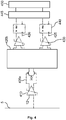
- Fig. 4 shows a schematic diagram of a second strand of a third analog-to-digital converter.
- the second strand represents a possible concrete implementation of the second strand of the Fig. 3
- the input circuit 10 is implemented as an input comparator 410, which compares the input signal 5 with the input reference value 12.
- the first first-level output signal of the input comparator 410 is forwarded to a differential stage 420a which, like the integrator 420b, is part of the integration circuit 20.
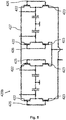
- the differential stage 420a converts the voltage signal of the input comparator 410 into a current signal different from that in Fig. 5 integrator 420b shown can be integrated.
- the integrator 420b has two branches, each branch comprising two capacitors.
- a branch is loaded in the half-period of the clock signal, in which the clock signal is high 425.
- the other branch is loaded in the half-period in which the clock signal is low 426.
- This is done by means of in Fig. 5 illustrated arrangement of normally-off transistors 422 and normally-on transistors 423 which either load or discharge the capacitors of the first or second branch depending on the clock signal (high or low).
- the charge on the capacitors is determined by means of two output comparators 430 included in the output circuit 30.
- An output comparator 430 is assigned to the first branch and another to the second branch of the integrator 420b.
- the outputs of the two output comparators 430 are in turn forwarded to an associated input of an associated time discretization circuit 440.
- the output of the first branch of the integrator 420 b associated output comparator 430 (lower part in the Fig. 4 or right part in the Fig. 5 ) is thus applied to an input of a first clocked flip-flop passed.
- the first clocked flip flop is clocked by the clock signal low 426.
- the output of output comparator 430 associated with the second branch of integrator 420b (upper part in FIG Fig. 4 or left part in the Fig. 5 ) is passed to an input of a second clocked flip-flop.
- the second clocked flip flop is clocked by the clock signal high 426.
- the two branches of the integrator 420b in combination with the two output comparators 430 of the output circuit 30 and the respectively assigned clocked flip-flops of the timing discretization circuit 440 allow the input signal 5 to be second in this case during both half cycles of the clock signal (second filter train with input reference values 12). convert discrete-time output signals 45.
- a multiplexer 445 is then used to assemble the time discrete output signals 45 of the two branches into a second discrete-time output signal and forward them to a translation unit 450 along with the first, third, and fourth time-discrete output signals.
- the translation unit 450 converts the thermometer code into a discrete-time binary output signal 305, as previously discussed.
- the multiplexer 445 may also be mounted behind the translation unit 450 in an alternative embodiment, such that the time-discrete output signals of the two branches of the respective string (or filter string 210) are first digitized by means of the translation unit 450 and only then through the multiplexer 445 to a time-discrete binary Output signal 305 are composed.
- the number of filter strings 210 or strings of the analog-to-digital converter is selected as a function of which resolution the time-discrete binary output signal 305 should make possible with respect to the input signal 5.
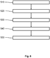
- Fig. 6 shows a schematic diagram of a method for filtering signals.
- an analogue input signal 5 is converted into at least two distinguishable first first-order output signals depending on the value of the input signal 5.
- this will be or integrated the first-stage output signals over a predetermined period.
- a first integration signal 25 is generated based on the result of the integration.
- the first integration signal 25 is compared with a first output reference value or output reference signal.
- step 550 based on the result of the comparison in step 540, a first two-stage output signal 35 is generated.
- the time-discrete output signal 45 can in turn be converted into a discrete-time binary output signal 305.
- An influence of higher-frequency fluctuations or disturbances on, for example, the digitization of analog input signals 5 compared to the given time period could thus be reduced since the digitization of the input signal no longer depends on a momentary value of the input signal 5.
Description
Die Erfindung bezieht sich auf eine Filterschaltung zur Filterung eines Eingangssignals eines Analog-Digital-Wandlers, einen Analog-Digital-Wandler und ein zugehöriges Verfahren zur Filterung eines Eingangssignals eines Analog-Digital-Wandlers.The invention relates to a filter circuit for filtering an input signal of an analog-to-digital converter, an analog-to-digital converter and an associated method for filtering an input signal of an analog-to-digital converter.
Ein Analog-Digital-Wandler (ADC) soll zu einem bestimmten, sich wiederholendem Zeitpunkt entscheiden, ob das Eingangssignal oberhalb oder unterhalb einer bestimmten Schwelle lag. Durch eine Mehrzahl von Schwellen entsteht so eine digitale Repräsentation des Signales zu jeweils einem Zeitpunkt der Clockperiode. Bei einem herkömmlichen ADC muss das Eingangssignal vor der Wandlung gefiltert werden (Antialiasing Filter). Dabei kann das Eingangssignal durch Rauschen oder Nichtlinearitäten gestört werden. Ein aktives Filter verbraucht zusätzliche Energie. Um ein Schwanken des Abtastzeitpunktes zu vermeiden, ist man zudem bemüht, bei dem Clocksignal möglichst scharfe Flanken zu erzeugen. Diese erzeugen durch parasitäre Kopplungen Störungen auf den internen Signalen des ADC, also zum Beispiel auch auf den Referenzspannungen, mit denen das Eingangssignal verglichen wird. Diese Schwankungen erzeugen Fehlentscheidungen der Komparatoren.An analog-to-digital converter (ADC) should decide at a certain, repetitive time whether the input signal was above or below a certain threshold. By a plurality of thresholds so creates a digital representation of the signal at each time of the clock period. In a conventional ADC, the input signal must be filtered before conversion (antialiasing filter). The input signal can be disturbed by noise or nonlinearities. An active filter consumes additional energy. In order to avoid a fluctuation of the sampling time, it is also endeavored to generate as sharp edges in the clock signal. These generate parasitic couplings disturbances on the internal signals of the ADC, so for example on the reference voltages with which the input signal is compared. These fluctuations create wrong decisions of the comparators.
Die
Es ist eine Aufgabe der vorliegenden Erfindung, eine verbesserte Filterschaltung insbesondere zur Filterung eines Eingangssignals eines Analog-Digital-Wandlers zur Verfügung zu stellen.It is an object of the present invention to provide an improved filter circuit, in particular for filtering an input signal of an analog-to-digital converter to provide.
Gemäß eines ersten Aspektes der Erfindung wird eine Filterschaltung zur Filterung eines Eingangssignals insbesondere eines analogen Eingangssignals zur Verfügung gestellt. Die Filterschaltung umfasst mindestens einen ersten Filterstrang. Der erste Filterstrang umfasst eine erste Eingangsschaltung, eine erste Integrationsschaltung und eine erste Ausgangsschaltung. Die erste Eingangsschaltung ist eingerichtet, ein analoges Eingangssignal in Abhängigkeit vom Wert des Eingangssignals in mindestens zwei unterscheidbare, erste erststufige Ausgangssignale umzuwandeln, und die erststufigen Ausgangssignale während eines vorgegebenen Zeitraums an die erste Integrationsschaltung weiterzuleiten. Die erste Integrationsschaltung ist zudem eingerichtet, die ersten erststufigen Ausgangssignale der ersten Eingangsschaltung über den vorgegebenen Zeitraum zu integrieren und ein erstes Integrationssignal zu erzeugen. Die erste Ausgangsschaltung ist eingerichtet, das erste Integrationssignal mit einem ersten Ausgangreferenzwert zu vergleichen und ein erstes zweitstufiges Ausgangssignal zu generieren.According to a first aspect of the invention, a filter circuit is provided for filtering an input signal, in particular an analog input signal. The filter circuit comprises at least a first filter strand. The first filter train comprises a first input circuit, a first integration circuit and a first output circuit. The first input circuit is arranged to convert an analog input signal into at least two distinguishable first first-level output signals depending on the value of the input signal, and to pass the first-stage output signals to the first integration circuit for a predetermined period of time. The first integration circuit is also configured to integrate the first first-stage output signals of the first input circuit over the predetermined period of time and to generate a first integration signal. The first output circuit is configured to compare the first integration signal with a first output reference value and generate a first second-level output signal.
Die Integration vermeidet, dass Veränderungen des Eingangssignals, insbesondere hochfrequente Störungen des Eingangssignals, die kürzer als der vorgegebene Zeitraum sind, keine bzw. nur einen geringfügigen Einfluss auf das Integrationsergebnis haben. Die ersten erststufigen Ausgangssignale sind dabei diskreter Natur. Ein Beispiel für diskrete erste erststufige Ausgangssignale wären die definierten Spannungen am Ausgang eines Komparators, der vergleicht, ob das Eingangssignal oberhalb oder unterhalb einer definierten Referenzspannung liegt. Die ersten erststufigen Ausgangssignale können kontinuierlich oder zeitdiskret ausgegeben werden.The integration avoids that changes in the input signal, in particular high-frequency interference of the input signal, which are shorter than the predetermined period, have no or only a minor influence on the integration result. The first first-stage output signals are discrete in nature. An example of discrete first-order output signals would be the defined voltages at the output of a comparator, which compares whether the input signal is above or below a defined reference voltage. The first first-stage output signals can be output continuously or time-discretely.
Der erste Filterstrang weist einen ersten Eingangsreferenzwert auf. Der erste Eingangsreferenzwert kann dabei fest vorgegeben oder frei programmierbar sein. Das Eingangssignal wird mit dem ersten Eingangsreferenzwert verglichen, um die ersten erststufigen Ausgangssignale zu bestimmen.The first filter train has a first input reference value. The first input reference value can be fixed or freely programmable. The input signal goes with the first one Input reference value compared to determine the first first-level output signals.
Das Eingangssignal wird durch die Eingangsschaltung in erste erststufige Ausgangssignale umgewandelt, die das Eingangssignal in dieser Ausführungsform in einen definierten Bezug zu dem definierten ersten Eingangsreferenzwert setzen. Zielsetzung dieser Referenzierung des Eingangssignals in dieser Ausführungsform ist es, die ersten erststufigen Ausgangssignale durch den Bezug zu dem definierten ersten Eingangsreferenzwert unterscheidbar zu machen. Die ersten erststufigen Ausgangssignale entsprechen dem Vorzeichen der Differenz des Eingangssignales minus des ersten Eingangsreferenzwertes. Der erste Eingangsreferenzwert weist einen diskreten Wert auf.The input signal is converted by the input circuit into first first-level output signals which in this embodiment place the input signal in a defined relation to the defined first input reference value. The purpose of this referencing of the input signal in this embodiment is to make the first first-order output signals distinguishable by reference to the defined first input reference value. The first first-level output signals correspond to the sign of the difference of the input signal minus the first input reference value. The first input reference value has a discrete value.
Die erste Eingangsschaltung umfasst vorzugsweise zumindest einen Eingangskomparator und die erste Ausgangsschaltung umfasst vorzugsweise mindestens einen Ausgangskomparator.The first input circuit preferably comprises at least one input comparator and the first output circuit preferably comprises at least one output comparator.
Die erste Integrationsschaltung weist vorzugsweise zumindest einen ersten Kondensator und erste Schalter auf. Der erste Kondensator und die ersten Schalter sind in dieser Ausführungsform eingerichtet, elektrische Ladungen, die den ersten erststufigen Ausgangssignalen zugeordnet sind über den vorgegebenen Zeitraum zu akkumulieren. Die ersten Schalter werden zum Beispiel so geschaltet dass während des vorgegebenen Zeitraums aufgrund der ersten erststufigen Ausgangssignale Ladungen auf den ersten Kondensator fließen. Die ersten Schalter werden am Ende des vorgegebenen Zeitraums so geschaltet, dass die während des vorgegebenen Zeitraums akkumulierte Ladung auf dem ersten Kondensator als Integrationssignal weitergeleitet bzw. der Ausgangsschaltung zur Verfügung gestellt werden kann. Sobald das Integrationssignal an die Ausgangsschaltung weitergeleitet wurde, werden die ersten Schalter so geschaltet, dass der erste Kondensator entladen wird. In einem nachfolgenden vorgegebenen Zeitraum kann der erste Kondensator wieder geladen werden, um erneut ein Integrationssignal zur Verfügung zu stellen.The first integration circuit preferably has at least a first capacitor and first switches. The first capacitor and the first switches are arranged in this embodiment to accumulate electrical charges associated with the first first-order output signals over the predetermined period of time. For example, the first switches are switched so that charges flow to the first capacitor during the predetermined period of time due to the first first-stage output signals. The first switches are switched at the end of the predetermined period so that the charge accumulated during the predetermined time period can be forwarded on the first capacitor as an integration signal or made available to the output circuit. Once the integration signal has been passed to the output circuit, the first switches are switched so that the first capacitor is discharged. In a subsequent predetermined period of time, the first capacitor be reloaded to provide an integration signal again.
Der vorgegebene Zeitraum wird vorzugsweise durch ein erstes regelmäßiges Zeitsignal vorgegeben. Das erste regelmäßige Zeitsignal kann zum Beispiel ein periodisches Clocksignal innerhalb einer Schaltungsanordnung sein. Dieses Clocksignal kann zum Beispiel eine Rechteckform aufweisen, wobei zumindest eine Halbperiode des Clocksignals zur Erzeugung des Integrationssignals verwendet wird.The predetermined period is preferably predetermined by a first regular time signal. The first regular time signal may, for example, be a periodic clock signal within a circuit arrangement. This clock signal may, for example, have a rectangular shape, wherein at least one half-period of the clock signal is used to generate the integration signal.
Der erste Filterstrang weist vorzugsweise eine erste Schaltung zur Zeitdiskreditierung auf. Die erste Schaltung zur Zeitdiskreditierung ist dabei dazu eingerichtet, das erste zweitstufige Ausgangssignal zu verarbeiten und in ein zeitdiskretes Ausgangssignal umzuwandeln. Beispiele für Schaltungen zur Zeitdiskreditierung sind getaktete Flipflops oder Latches. Die erste Schaltung zur Zeitdiskreditierung ist vorzugsweise eingerichtet, das erste zweitstufige Ausgangssignal in Abhängigkeit von dem ersten regelmäßigen, insbesondere periodischen Zeitsignal in das erste zeitdiskrete Ausgangssignal umzuwandeln.The first filter string preferably has a first time-discriminating circuit. The first circuit for time discrediting is configured to process the first two-stage output signal and convert it into a time-discrete output signal. Examples of time discriminating circuits are clocked flip-flops or latches. The first circuit for time-discriminating is preferably set up to convert the first two-stage output signal into the first time-discrete output signal as a function of the first periodic, in particular periodic, time signal.
Die Filterschaltung umfasst vorzugsweise mindestens einen zweiten Filterstrang, wobei dem ersten Filterstrang ein erster Bereich des Eingangssignals zugeordnet ist und dem zweiten Filterstrang ein zweiter Bereich des Eingangssignals zugeordnet ist, wobei sich der erste Bereich des Eingangssignals vom zweiten Bereich des Eingangssignals unterscheidet.The filter circuit preferably comprises at least one second filter train, wherein the first filter strand is assigned a first region of the input signal and the second filter strand is assigned a second region of the input signal, wherein the first region of the input signal differs from the second region of the input signal.
Der erste und der zweite Bereich können sich teilweise überlappen. Der zweite Filterstrang umfasst eine zweite Eingangsschaltung, eine zweite Integrationsschaltung und eine zweite Ausgangschaltung. Die zweite Eingangsschaltung erzeugt ein zweites erststufiges Ausgangssignal. Die Integrationsschaltung erzeugt ein zweites Integrationssignal. Die Ausgangsschaltung erzeugt ein zweites zweitstufiges Ausgangssignal. Der erste Filterstrang ist somit eingerichtet, den ersten Bereich des Eingangssignals in der zuvor beschriebenen Art und Weise zu filtern. Der zweite Filterstrang ist somit eingerichtet, den zweiten Bereich des Eingangssignals in der zuvor beschriebenen Art und Weise zu filtern.The first and second areas may partially overlap. The second filter train comprises a second input circuit, a second integration circuit and a second output circuit. The second input circuit generates a second first-level output signal. The integration circuit generates a second integration signal. The output circuit generates a second two-stage output signal. The first filter train is thus arranged to filter the first range of the input signal in the manner previously described. The second filter strand is thus configured to filter the second region of the input signal in the manner previously described.
Die Filterschaltung umfasst vorzugsweise mindestens einen dritten Filterstrang, wobei dem dritten Filterstrang ein dritter Bereich des Eingangssignals zugeordnet ist, wobei der zweite Bereich des Eingangssignals an den ersten Bereich des Eingangssignals grenzt, und der dritte Bereich des Eingangssignals an den zweiten Bereich des Eingangssignals grenzt. Der dritte Filterstrang umfasst eine dritte Eingangsschaltung, eine dritte Integrationsschaltung und eine dritte Ausgangschaltung. Die dritte Eingangsschaltung erzeugt ein drittes erststufiges Ausgangssignal. Die Integrationsschaltung erzeugt ein drittes Integrationssignal. Die dritte Ausgangsschaltung erzeugt ein drittes zweitstufiges Ausgangssignal. Der dritte Filterstrang ist somit eingerichtet, den dritten Bereich des Eingangssignals in der zuvor beschriebenen Art und Weise zu filtern. Die Filterschaltung kann weitere Filterstränge (4, 5, 6 oder mehr) aufweisen, so dass dem Eingangssignal mittels der Filterstränge eine Vielzahl von zweitstufigen Ausgangssignalen bzw. zeitdiskreten Ausgangssignalen zugewiesen werden kann.The filter circuit preferably comprises at least one third filter train, wherein the third filter strand is associated with a third region of the input signal, the second region of the input signal adjacent to the first region of the input signal, and the third region of the input signal adjacent to the second region of the input signal. The third filter train comprises a third input circuit, a third integration circuit and a third output circuit. The third input circuit generates a third first-level output signal. The integration circuit generates a third integration signal. The third output circuit generates a third two-stage output signal. The third filter string is thus arranged to filter the third region of the input signal in the manner described above. The filter circuit may comprise further filter strands (4, 5, 6 or more), so that a plurality of second-stage output signals or time-discrete output signals can be assigned to the input signal by means of the filter strands.
Der erste Bereich, der zweite Bereich, der dritte Bereich und weitere Bereiche des Eingangssignals sind vorzugsweise gleich groß. Das Eingangssignal kann somit in eine Vielzahl von gleichgroßen Bereichen aufgeteilt werden, für die die zweitstufigen Ausgangssignale bzw. zeitdiskreten Ausgangssignale mittels der einzelnen Filterstränge der Filterschaltung bestimmt werden.The first area, the second area, the third area and further areas of the input signal are preferably the same size. The input signal can thus be divided into a plurality of equally sized areas for which the second-stage output signals or time-discrete output signals are determined by means of the individual filter strings of the filter circuit.
Der erste Filterstrang weist vorzugsweise einen ersten Eingangsreferenzwert, der zweite Filterstrang einen zweiten Eingangsreferenzwert und der dritte Filterstrang einen dritten Eingangsreferenzwert auf. Der erste Bereich wird mittels des ersten Eingangsreferenzwerts zugeordnet. Der zweite Bereich wird mittels des zweiten Eingangsreferenzwerts zugeordnet. Der dritte Bereich wird mittels des dritten Eingangsreferenzwerts zugeordnet.The first filter string preferably has a first input reference value, the second filter string has a second input reference value, and the third filter string has a third input reference value. The first range is assigned by means of the first input reference value. The second area is by means of the second Assigned to input reference value. The third area is assigned by means of the third input reference value.
In einer bevorzugten Ausführungsform wird mittels des ersten zweitstufigen Ausgangssignals, eines mittels des zweiten Filterstrangs erzeugten zweiten zweitstufigen Ausgangssignals, und eines mittels des dritten Filterstrang erzeugten dritten zweitstufigen Ausgangssignals ein Thermometerkode erzeugt. Das zeitdiskrete Ausgangssignal ist vorzugsweise ein zeitdiskreter Thermometerkode.In a preferred embodiment, a thermometer code is generated by means of the first two-stage output signal, a second second-stage output signal generated by means of the second filter string, and a third two-stage output signal generated by means of the third filter string. The discrete-time output signal is preferably a time-discrete thermometer code.
Es ist eine weitere Aufgabe der vorliegenden Erfindung, einen verbesserten Analog-Digital-Wandler zur Verfügung zu stellen.It is another object of the present invention to provide an improved analog-to-digital converter.
Der Analog-Digital-Wandler umfasst vorzugsweise eine Filterschaltung, die in der zuvor geschilderten Weise einen zeitdiskreten Thermometerkode erzeugt. Der Analog-Digital-Wandler umfasst des Weiteren eine Übersetzungseinheit, wobei die Übersetzungseinheit eingerichtet ist, den zeitdiskreten Thermometerkode in ein zeitdiskretes binäres Ausgangssignal umzuwandeln.The analog-to-digital converter preferably comprises a filter circuit which generates a time-discrete thermometer code in the manner described above. The analog-digital converter further comprises a translation unit, wherein the translation unit is adapted to convert the discrete-time thermometer code into a discrete-time binary output signal.
Es ist eine weitere Aufgabe der vorliegenden Erfindung, ein verbessertes Verfahren zur Filterung von Signalen zur Verfügung zu stellen. Das Verfahren umfasst die Schritte:
- Umwandeln eines Eingangssignals in Abhängigkeit vom Wert des Eingangssignals in mindestens zwei unterscheidbare erste erststufige Ausgangssignale, wobei das Eingangssignal mit einem ersten Eingangsreferenzwert verglichen wird, um die ersten erststufigen Ausgangssignale zu bestimmen, wobei die ersten erststufigen Ausgangssignale dem Vorzeichen der Differenz des Eingangssignales minus des ersten Eingangsreferenzwert entsprechen,
- Integrieren der ersten erststufigen Ausgangssignale über einen vorgegebenen Zeitraum,
- Erzeugen eines ersten Integrationssignals basierend auf dem Ergebnis der Integration,
- Vergleichen des ersten Integrationssignals mit einem ersten Ausgangsreferenzwert, und
- Generieren eines ersten zweitstufigen Ausgangssignals basierend auf dem Ergebnis des Vergleichs.
- Converting an input signal into at least two distinguishable first-stage output signals in response to the value of the input signal, wherein the input signal is compared to a first input reference value to determine the first first-order output signals, the first first-order output signals being the sign of the difference of the input signal minus the first input reference value correspond,
- Integrating the first first-stage output signals over a predetermined period of time,
- Generating a first integration signal based on the result of the integration,
- Comparing the first integration signal with a first output reference value, and
- Generating a first two-stage output signal based on the result of the comparison.
Die einzelnen Schritte des Verfahrens müssen nicht notwendigerweise in der angegebenen Reihenfolge durchgeführt werden.The individual steps of the method need not necessarily be carried out in the order given.
Es wird klargestellt, dass die Filterschaltung gemäß Anspruch 1, der Analog-Digital-Wandler gemäß Anspruch 13 und das Verfahren gemäß Anspruch 14 ähnliche und/oder identische Ausführungsform aufweisen, wie sie insbesondere in den abhängigen Ansprüchen beschrieben werden.It will be understood that the filter circuit of claim 1, the analog-to-digital converter of
Es wird weiterhin klargestellt, dass bevorzugte Ausführungsformen der Erfindung auch jede Kombination der abhängigen Ansprüche mit dem entsprechenden unabhängigen Anspruch darstellen.It is further clarified that preferred embodiments of the invention also represent any combination of the dependent claims with the corresponding independent claim.
Weitere bevorzugte Ausführungsformen werden im Folgenden beschrieben.Further preferred embodiments are described below.
Diese und andere Aspekte der Erfindung werden im Detail in den Abbildungen wie folgt gezeigt.
-
Fig. 1 zeigt eine Prinzipskizze einer ersten Filterschaltung -
Fig. 2 zeigt eine Prinzipskizze eines ersten Analog-Digital-Wandlers -
Fig. 3 zeigt eine Prinzipskizze eines zweiten Analog-Digital-Wandlers -
Fig. 4 zeigt eine Prinzipskizze eines Stranges eines dritten Analog-Digital-Wandlers -
Fig. 5 zeigt eine Prinzipskizze eines Integrators einer Integrationsschaltung -
Fig. 6 zeigt eine Prinzipskizze eines Verfahrens zur Filterung von Signalen
-
Fig. 1 shows a schematic diagram of a first filter circuit -
Fig. 2 shows a schematic diagram of a first analog-to-digital converter -
Fig. 3 shows a schematic diagram of a second analog-to-digital converter -
Fig. 4 shows a schematic diagram of a strand of a third analog-to-digital converter -
Fig. 5 shows a schematic diagram of an integrator of an integration circuit -
Fig. 6 shows a schematic diagram of a method for filtering signals
Eine solche Filterschaltung 200 könnte insbesondere in Analog-Digital-Wandlern Anwendung finden. Im Unterschied zu herkömmlichen Analog-Digital-Wandlern würde das analoge Signal nicht zu einem einzigen Zeitpunkt zu einem digitalen Signal umgewandelt werden, wobei dieser Zeitpunkt zum Beispiel durch die Flanke eines Clocksignals vorgegeben wäre. Das analoge Signal würde vielmehr über einen vorgegebenen Zeitraum, der zum Beispiel einer Halbperiode des Clocksignals entsprechen könnte, integriert werden. Das Integrationssignal würde dann zur Erzeugung des digitalen Signals verwendet werden. Dies hätte den Vorteil, dass kurzzeitigen Schwankungen oder Störungen des Eingangssignals 5, die kürzer als eine Halbperiode des Clocksignals sind, einen deutlich verringerten Einfluss auf das Ergebnis der Digitalisierung haben würden. Die kurzzeitigen Schwankungen oder Störung des Eingangssignals 5 sind vorzugsweise kürzer als die Hälfte, ein Drittel, ein Fünftel oder zum Beispiel ein Zehntel des vorgegebenen Zeitraums (in diesem Fall eine Halbperiode des Clocksignals).Such a
Es ist eine Idee der vorliegenden Erfindung ein Eingangssignal 5 über einen vorgegebenen Zeitraum zu integrieren, und das Ergebnis der Integration in ein zeitdiskretes Ausgangssignal 45 umzuwandeln. Das zeitdiskrete Ausgangssignal 45 kann wiederum in ein zeitdiskretes binäres Ausgangssignal 305 umgewandelt werden. Ein Einfluss von im Vergleich zum vorgegebenen Zeitraum höherfrequenten Schwankungen oder Störungen auf zum Beispiel die Digitalisierung von analogen Eingangssignalen 5 könnte somit vermindert werden, da die Digitalisierung des Eingangssignals nicht mehr von einem momentanen Wert des Eingangssignals 5 abhängt.It is an idea of the present invention to integrate an
Eine entsprechend angepasste Filterschaltung kann zum Beispiel in einem Analog-Digital-Wandler (ADC) verwendet werden. Der ADC arbeitet in drei Stufen:
- 1) Wertdiskretisierung: Das Eingangssignal wird mit Hilfe von zum Beispiel n-1 Verstärkern (Gleichrichter) für n Bits kontinuierlich digitalisiert. Das Ausgangsignal der Verstärker entspricht dem Vorzeichen des Eingangssignales minus des jeweiligen Referenzwertes. Auf diese Weise entsteht nach den Verstärkern ein kontinuierlicher Thermometerkode des Eingangssignales.
- 2) periodische Integration: Jedes Bit des Thermometerkodes wird für sich über eine Halbperiode eines Clocksignals integriert. Das Ausgangssignal der Integrationsschaltung ist das Vorzeichen ob das jeweilige Bit des Thermometerkodes während der Halbperiode öfter -1 oder +1 war.
- 3) Zeitdiskretisierung: Am Ende der Halbperiode erfasst ein getakteter Verstärker ob das Ausgangsignal der Integrationsschaltung am Ende des Integrationszeitraumes -1 oder +1 ist.
- 4) Konvertierung: Das zeitdiskreditierte Ausgangssignal wird nach dem Abtasten vom Thermometerkode in binären Kode konvertiert.
- 1) Value Discretization: The input signal is continuously digitized by means of, for example, n-1 amplifiers (rectifiers) for n bits. The output signal of the amplifiers corresponds to the sign of the input signal minus the respective reference value. In this way, after the amplifiers, a continuous thermometer code of the input signal is produced.
- 2) Periodic integration: Each bit of the thermometer code is integrated on its own for a half-period of a clock signal. The output of the integrator circuit is the sign whether the particular bit of the thermometer code was -1 or +1 more during the half period.
- 3) Time Discretization: At the end of the half-period, a clocked clock is detected Amplifier whether the output signal of the integration circuit at the end of the integration period is -1 or +1.
- 4) Conversion: The time-discriminated output signal is converted to binary code by the thermometer code after sampling.
Weitere Varianten der Erfindung und ihre Ausführung ergeben sich für den Fachmann aus der vorangegangenen Offenbarung, den Figuren und den Patentansprüchen.Other variants of the invention and their execution will become apparent to those skilled in the art from the foregoing disclosure, the drawings and the claims.
In den Patentansprüchen verwendete Begriffe wie "umfassen", "aufweisen", "beinhalten", "enthalten" und dergleichen schließen weitere Elemente oder Schritte nicht aus. Die Verwendung des unbestimmten Artikels schließt eine Mehrzahl nicht aus. Eine einzelne Einrichtung kann die Funktionen mehrerer in den Patentansprüchen genannten Einheiten bzw. Einrichtungen ausführen. In den Patentansprüchen angegebene Bezugszeichen sind nicht als Beschränkungen der eingesetzten Mittel und Schritte anzusehen.Terms used in the claims, such as "comprising,""comprising,""including,""containing," and the like, do not exclude other elements or steps. The use of the indefinite article does not exclude a majority. A single device can perform the functions of several units or devices mentioned in the claims. Reference signs indicated in the claims should not be regarded as limitations on the means and steps employed.
- 55
- Eingangssignalinput
- 1010
- Eingangsschaltunginput circuit
- 11, 12, 13, 1411, 12, 13, 14
- EingangsreferenzwertInput reference value
- 2020
- Integrationsschaltungintegration circuit
- 2525
- Integrationssignalintegration signal
- 3030
- Ausgangsschaltungoutput circuit
- 3535
- zweitstufiges Ausgangssignalsecond-level output signal
- 40, 44040, 440
- Schaltung zur ZeitdiskreditierungCircuit for time discrediting
- 4545
- zeitdiskretes Ausgangssignaldiscrete-time output signal
- 50, 45050, 450
- Übersetzungseinheittranslation unit
- 200200
- Filterschaltungfilter circuit
- 210210
- Filterstrangfilter rod
- 300300
- Analog-Digital-WandlerAnalog to digital converter
- 305305
- zeitdiskretes binäres Ausgangssignaldiscrete-time binary output signal
- 410410
- Eingangskomparatorinput comparator
- 420a420a
- Differenzstufedifferential stage
- 420b420b
- Integratorintegrator
- 422422
- selbstsperrender Transistorself-locking transistor
- 423423
- selbstleitender Transistorself-conducting transistor
- 425425
- Clock highClock high
- 426426
- Clock lowClock low
- 427427
- Versorgungsspannungsupply voltage
- 430430
- Ausgangskomparatoroutput comparator
- 445445
- Multiplexermultiplexer
- 510510
- Umwandeln eines analogen EingangssignalsConvert an analog input signal
- 520520
- Integrieren von erststufigen AusgangssignalenIntegrate first-stage output signals
- 530530
- Erzeugen eines IntegrationssignalsGenerating an integration signal
- 540540
- Vergleich Integrationssignal AusgangsreferenzwertComparison of integration signal output reference value
- 550550
- Generieren eines zweitstufigen AusgangssignalsGenerating a second-level output signal
Claims (12)
- A filter circuit (200) comprising at least a first filter line (210), wherein the first filter line (210) comprises a first input circuit (10), a first integration circuit (20) and a first output circuit (30), wherein the first filter line (210) comprises a first input reference value (11, 12, 13, 14), wherein the first input circuit (10) is configured in such a way that, as a function of the value of the input signal, it converts an input signal (5) into at least two distinguishable, first first-stage output signals, wherein the input signal is compared to the first input reference value (11, 12, 13, 14) to determine the first first-stage output signals, wherein the first first-stage output signals correspond to a mathematical sign of the difference of the input signal (5) minus the first input reference value (11, 12, 13, 14), wherein the first input circuit (10) is further configured to relay the first-stage output signals to the first integration circuit (20, 420) during a predefined period of time, wherein the first integration circuit (20) is configured to integrate the first first-stage output signals of the first input circuit (10) over the predefined period of time and to generate a first integration signal (25), and wherein the first output circuit (30) is configured to compare the first integration signal (25) to a first output reference value and to generate a first second-stage output signal (35).
- The filter circuit (200) according to any one of the preceding claims, wherein the first input circuit (10) comprises at least an input comparator (410) and the first output circuit (30) comprises at least an output comparator (430).
- The filter circuit (200) according to any one of the preceding claims, wherein the first integration circuit (20) comprises at least a first capacitor and first switches, wherein the first capacitor and the first switches are configured so that, over the predefined period of time, they accumulate electric charges that are associated with the first first-stage output signals.
- The filter circuit (200) according to any one of the preceding claims, wherein the predefined period of time is predefined by a first regular time signal.
- The filter circuit (200) according to any one of the preceding claims, wherein the first filter line (210) comprises a first circuit for time discretization (40, 440), and wherein the first circuit for the time discretization (40, 440) is configured to process the first second-stage output signal and to generate a time-discrete output signal (45).
- The filter circuit (200) according to claim 5 to the extent that claim 5 refers back to claim 4, wherein the first circuit for the time discretization (40, 440) is configured to convert the first second-stage output signal (35) into the first time-discrete output signal (45) as a function of the first regular time signal.
- The filter circuit (200) according to any one of the preceding claims, wherein the filter circuit comprises at least a second filter line (210), wherein a first range of the input signal is associated with the first filter line (210), and wherein a second range of the input signal (5) is associated with the second filter line (210), wherein the first range of the input signal (5) differs from the second range of the input signal (5).
- The filter circuit (200) according to claim 7, further comprising at least a third filter line (210), wherein a third range of the input signal (5) is associated with the third filter line (210), wherein the second range of the input signal (5) adjoins the first range of the input signal (5), and the third range of the input signal (5) adjoins the second range of the input signal (5).
- The filter circuit (200) according to claim 8 to the extent that claim 8 refers back to the claims 1 to 7, wherein the second filter line (210) comprises a second input reference value (11, 12, 13, 14), and wherein the third filter line (210) comprises a third input reference value (11, 12, 13, 14), wherein the first range is associated by means of the first input reference value (11, 12, 13, 14), the second range is associated by means of the second input reference value (11, 12, 13, 14), and the third range is associated by means of the third input reference value (11, 12, 13, 14).
- The filter circuit (200) according to one of the claims 8 or 9, wherein a thermometer code is generated by means of the first second-stage output signal (35), by means of a second second-stage output signal (35) generated by the second filter line (210), and by means of a third second-stage output signal (35) generated by the third filter line (210).
- An analog-to-digital converter comprising a filter circuit (200) according to claim 10 and a transformation unit (50), wherein the transformation unit (50) is configured to convert the time-discrete thermometer code into a time-discrete binary output signal (305).
- A method for filtering signals, comprising the following steps:- converting an input signal (5), as a function of the value of the input signal (5), into at least two distinguishable first first-stage output signals, wherein the input signal is compared to a first input reference value (11, 12, 13, 14) to determine the first first-stage output signals, wherein the first first-stage output signals correspond to a mathematical sign of the difference of the input signal (5) minus the first input reference value (11, 12, 13, 14);- integrating the first first-stage output signals over a predefined period of time;- generating a first integration signal (25) on the basis of the result of the integration;- comparing the first integration signal (25) to a first output reference value; and- generating a first second-stage output signal (35) on the basis of the result of the comparison.
Applications Claiming Priority (2)
| Application Number | Priority Date | Filing Date | Title |
|---|---|---|---|
| DE102015212848.2A DE102015212848A1 (en) | 2015-07-09 | 2015-07-09 | Filter circuit for filtering an input signal of an analog-to-digital converter |
| PCT/EP2016/065856 WO2017005745A1 (en) | 2015-07-09 | 2016-07-05 | Filter circuit for filtering an input signal of an analogue-to-digital converter |
Publications (2)
| Publication Number | Publication Date |
|---|---|
| EP3320618A1 EP3320618A1 (en) | 2018-05-16 |
| EP3320618B1 true EP3320618B1 (en) | 2019-05-22 |
Family
ID=56550187
Family Applications (1)
| Application Number | Title | Priority Date | Filing Date |
|---|---|---|---|
| EP16742192.4A Active EP3320618B1 (en) | 2015-07-09 | 2016-07-05 | Filter circuit for filtering an input signal of an analogue-to-digital converter |
Country Status (6)
| Country | Link |
|---|---|
| US (1) | US10284214B2 (en) |
| EP (1) | EP3320618B1 (en) |
| JP (1) | JP2018526868A (en) |
| CN (1) | CN108028660B (en) |
| DE (1) | DE102015212848A1 (en) |
| WO (1) | WO2017005745A1 (en) |
Families Citing this family (2)
| Publication number | Priority date | Publication date | Assignee | Title |
|---|---|---|---|---|
| AU2019340530A1 (en) | 2018-09-12 | 2021-03-11 | Eucure (Beijing) Biopharma Co., Ltd | Anti-TNFRSF9 antibodies and uses thereof |
| CN109283383B (en) * | 2018-10-19 | 2020-08-28 | 深圳市计量质量检测研究院 | Method and device for measuring voltage fluctuation value of rectangular modulation voltage and storage medium |
Family Cites Families (8)
| Publication number | Priority date | Publication date | Assignee | Title |
|---|---|---|---|---|
| JP3465433B2 (en) | 1995-09-05 | 2003-11-10 | 三菱電機株式会社 | Disk contact detection circuit for MR head |
| US5990707A (en) * | 1997-09-05 | 1999-11-23 | Cirrus Logic, Inc. | Method and system for sliced integration of flash analog to digital converters in read channel circuits |
| US5990814A (en) * | 1997-09-05 | 1999-11-23 | Cirrus Logic, Inc. | Method and circuit for calibration of flash analog to digital converters |
| US6366231B1 (en) * | 2000-04-10 | 2002-04-02 | General Electric Company | Integrate and fold analog-to-digital converter with saturation prevention |
| JP3820947B2 (en) * | 2001-09-21 | 2006-09-13 | ヤマハ株式会社 | Class D amplifier |
| JP2010199798A (en) * | 2009-02-24 | 2010-09-09 | Renesas Electronics Corp | Analog/digital conversion circuit |
| CN101741387B (en) * | 2009-12-17 | 2013-03-27 | 上海贝岭股份有限公司 | Integral analogue-to-digital converter and sampling control method thereof |
| JP5471761B2 (en) * | 2010-04-15 | 2014-04-16 | 富士通株式会社 | Receiver circuit |
-
2015
- 2015-07-09 DE DE102015212848.2A patent/DE102015212848A1/en not_active Withdrawn
-
2016
- 2016-07-05 WO PCT/EP2016/065856 patent/WO2017005745A1/en active Application Filing
- 2016-07-05 EP EP16742192.4A patent/EP3320618B1/en active Active
- 2016-07-05 US US15/743,123 patent/US10284214B2/en active Active
- 2016-07-05 CN CN201680040634.7A patent/CN108028660B/en active Active
- 2016-07-05 JP JP2018500574A patent/JP2018526868A/en not_active Ceased
Non-Patent Citations (1)
| Title |
|---|
| None * |
Also Published As
| Publication number | Publication date |
|---|---|
| DE102015212848A1 (en) | 2017-01-12 |
| JP2018526868A (en) | 2018-09-13 |
| CN108028660A (en) | 2018-05-11 |
| US20180351566A1 (en) | 2018-12-06 |
| WO2017005745A1 (en) | 2017-01-12 |
| EP3320618A1 (en) | 2018-05-16 |
| CN108028660B (en) | 2021-08-17 |
| US10284214B2 (en) | 2019-05-07 |
Similar Documents
| Publication | Publication Date | Title |
|---|---|---|
| DE102016119246B4 (en) | Low-noise precision input stage for analog-to-digital converters | |
| EP2936201B1 (en) | Device for determining a property of a transmission channel between a transmitter and a receiver | |
| EP0452609B1 (en) | High resolution monolithic integrated analog-digital converter | |
| DE102011005325A1 (en) | Cyclic analog / digital converter | |
| EP3320618B1 (en) | Filter circuit for filtering an input signal of an analogue-to-digital converter | |
| DE102015102050A1 (en) | ANALOG-DIGITAL CONVERSION | |
| DE102014100656A1 (en) | Time-continuous input stage | |
| EP2087596A1 (en) | Measurement amplification device and method | |
| DE102019121425A1 (en) | Multiplexed sigma-delta analog-to-digital converter | |
| DE60125785T2 (en) | FAST PRECISION ANALOG / DIGITAL TRANSFER | |
| EP2850731B1 (en) | Procedure for supressing a disturbance in a sampling process and a device for executing the procedure | |
| DE102019133928A1 (en) | Arrangement for a vehicle | |
| DE102014204518A1 (en) | Circuitry, analog-to-digital converter, gradient amplifier and method for suppressing offset, offset drift and 1 / f noise of one of the analog-to-digital conversion | |
| DE102015110450B4 (en) | Sensor systems with multi-mode analog-digital conversion | |
| DE102018104530B4 (en) | Sigma-delta converters and corresponding methods | |
| DE102016119244B4 (en) | Time to digital converter | |
| DE112008001033T5 (en) | A / D Converter | |
| DE2155839A1 (en) | FREQUENCY-VOLTAGE CONVERTERS, IN PARTICULAR FOR BLOCKING AND SLIP PROTECTION DEVICES OF VEHICLES | |
| DE602004009779T2 (en) | Device for converting an analog signal into a digital signal, corresponding method and voltage regulator control circuit with this device | |
| DE112014002775T5 (en) | Capacitive measuring system and method | |
| DE102016014124A1 (en) | Method for measuring a capacitance value | |
| DE10258783B4 (en) | Method for analog-to-digital conversion and analog-to-digital converter | |
| DE102010029693A1 (en) | Circuit arrangement for detecting a fault of a converter | |
| DE3933801A1 (en) | ADAPTIVE DEVICE FOR IDENTIFYING A PERIODIC SIGNAL | |
| DE102019009175B4 (en) | Analog-digital converter and sensor arrangement containing it |
Legal Events
| Date | Code | Title | Description |
|---|---|---|---|
| STAA | Information on the status of an ep patent application or granted ep patent |
Free format text: STATUS: THE INTERNATIONAL PUBLICATION HAS BEEN MADE |
|
| PUAI | Public reference made under article 153(3) epc to a published international application that has entered the european phase |
Free format text: ORIGINAL CODE: 0009012 |
|
| STAA | Information on the status of an ep patent application or granted ep patent |
Free format text: STATUS: REQUEST FOR EXAMINATION WAS MADE |
|
| 17P | Request for examination filed |
Effective date: 20180209 |
|
| AK | Designated contracting states |
Kind code of ref document: A1 Designated state(s): AL AT BE BG CH CY CZ DE DK EE ES FI FR GB GR HR HU IE IS IT LI LT LU LV MC MK MT NL NO PL PT RO RS SE SI SK SM TR |
|
| AX | Request for extension of the european patent |
Extension state: BA ME |
|
| RIN1 | Information on inventor provided before grant (corrected) |
Inventor name: GREWING, CHRISTIAN |
|
| DAV | Request for validation of the european patent (deleted) | ||
| DAX | Request for extension of the european patent (deleted) | ||
| GRAP | Despatch of communication of intention to grant a patent |
Free format text: ORIGINAL CODE: EPIDOSNIGR1 |
|
| STAA | Information on the status of an ep patent application or granted ep patent |
Free format text: STATUS: GRANT OF PATENT IS INTENDED |
|
| INTG | Intention to grant announced |
Effective date: 20190116 |
|
| GRAS | Grant fee paid |
Free format text: ORIGINAL CODE: EPIDOSNIGR3 |
|
| GRAA | (expected) grant |
Free format text: ORIGINAL CODE: 0009210 |
|
| STAA | Information on the status of an ep patent application or granted ep patent |
Free format text: STATUS: THE PATENT HAS BEEN GRANTED |
|
| AK | Designated contracting states |
Kind code of ref document: B1 Designated state(s): AL AT BE BG CH CY CZ DE DK EE ES FI FR GB GR HR HU IE IS IT LI LT LU LV MC MK MT NL NO PL PT RO RS SE SI SK SM TR |
|
| REG | Reference to a national code |
Ref country code: GB Ref legal event code: FG4D Free format text: NOT ENGLISH |
|
| REG | Reference to a national code |
Ref country code: CH Ref legal event code: EP |
|
| REG | Reference to a national code |
Ref country code: IE Ref legal event code: FG4D Free format text: LANGUAGE OF EP DOCUMENT: GERMAN |
|
| REG | Reference to a national code |
Ref country code: DE Ref legal event code: R096 Ref document number: 502016004813 Country of ref document: DE |
|
| REG | Reference to a national code |
Ref country code: AT Ref legal event code: REF Ref document number: 1137318 Country of ref document: AT Kind code of ref document: T Effective date: 20190615 |
|
| REG | Reference to a national code |
Ref country code: SE Ref legal event code: TRGR |
|
| REG | Reference to a national code |
Ref country code: NL Ref legal event code: MP Effective date: 20190522 |
|
| REG | Reference to a national code |
Ref country code: LT Ref legal event code: MG4D |
|
| PG25 | Lapsed in a contracting state [announced via postgrant information from national office to epo] |
Ref country code: AL Free format text: LAPSE BECAUSE OF FAILURE TO SUBMIT A TRANSLATION OF THE DESCRIPTION OR TO PAY THE FEE WITHIN THE PRESCRIBED TIME-LIMIT Effective date: 20190522 Ref country code: PT Free format text: LAPSE BECAUSE OF FAILURE TO SUBMIT A TRANSLATION OF THE DESCRIPTION OR TO PAY THE FEE WITHIN THE PRESCRIBED TIME-LIMIT Effective date: 20190922 Ref country code: NL Free format text: LAPSE BECAUSE OF FAILURE TO SUBMIT A TRANSLATION OF THE DESCRIPTION OR TO PAY THE FEE WITHIN THE PRESCRIBED TIME-LIMIT Effective date: 20190522 Ref country code: ES Free format text: LAPSE BECAUSE OF FAILURE TO SUBMIT A TRANSLATION OF THE DESCRIPTION OR TO PAY THE FEE WITHIN THE PRESCRIBED TIME-LIMIT Effective date: 20190522 Ref country code: LT Free format text: LAPSE BECAUSE OF FAILURE TO SUBMIT A TRANSLATION OF THE DESCRIPTION OR TO PAY THE FEE WITHIN THE PRESCRIBED TIME-LIMIT Effective date: 20190522 Ref country code: HR Free format text: LAPSE BECAUSE OF FAILURE TO SUBMIT A TRANSLATION OF THE DESCRIPTION OR TO PAY THE FEE WITHIN THE PRESCRIBED TIME-LIMIT Effective date: 20190522 Ref country code: NO Free format text: LAPSE BECAUSE OF FAILURE TO SUBMIT A TRANSLATION OF THE DESCRIPTION OR TO PAY THE FEE WITHIN THE PRESCRIBED TIME-LIMIT Effective date: 20190822 |
|
| PG25 | Lapsed in a contracting state [announced via postgrant information from national office to epo] |
Ref country code: RS Free format text: LAPSE BECAUSE OF FAILURE TO SUBMIT A TRANSLATION OF THE DESCRIPTION OR TO PAY THE FEE WITHIN THE PRESCRIBED TIME-LIMIT Effective date: 20190522 Ref country code: GR Free format text: LAPSE BECAUSE OF FAILURE TO SUBMIT A TRANSLATION OF THE DESCRIPTION OR TO PAY THE FEE WITHIN THE PRESCRIBED TIME-LIMIT Effective date: 20190823 Ref country code: LV Free format text: LAPSE BECAUSE OF FAILURE TO SUBMIT A TRANSLATION OF THE DESCRIPTION OR TO PAY THE FEE WITHIN THE PRESCRIBED TIME-LIMIT Effective date: 20190522 Ref country code: BG Free format text: LAPSE BECAUSE OF FAILURE TO SUBMIT A TRANSLATION OF THE DESCRIPTION OR TO PAY THE FEE WITHIN THE PRESCRIBED TIME-LIMIT Effective date: 20190822 |
|
| PG25 | Lapsed in a contracting state [announced via postgrant information from national office to epo] |
Ref country code: SK Free format text: LAPSE BECAUSE OF FAILURE TO SUBMIT A TRANSLATION OF THE DESCRIPTION OR TO PAY THE FEE WITHIN THE PRESCRIBED TIME-LIMIT Effective date: 20190522 Ref country code: DK Free format text: LAPSE BECAUSE OF FAILURE TO SUBMIT A TRANSLATION OF THE DESCRIPTION OR TO PAY THE FEE WITHIN THE PRESCRIBED TIME-LIMIT Effective date: 20190522 Ref country code: CZ Free format text: LAPSE BECAUSE OF FAILURE TO SUBMIT A TRANSLATION OF THE DESCRIPTION OR TO PAY THE FEE WITHIN THE PRESCRIBED TIME-LIMIT Effective date: 20190522 Ref country code: RO Free format text: LAPSE BECAUSE OF FAILURE TO SUBMIT A TRANSLATION OF THE DESCRIPTION OR TO PAY THE FEE WITHIN THE PRESCRIBED TIME-LIMIT Effective date: 20190522 Ref country code: EE Free format text: LAPSE BECAUSE OF FAILURE TO SUBMIT A TRANSLATION OF THE DESCRIPTION OR TO PAY THE FEE WITHIN THE PRESCRIBED TIME-LIMIT Effective date: 20190522 |
|
| REG | Reference to a national code |
Ref country code: DE Ref legal event code: R097 Ref document number: 502016004813 Country of ref document: DE |
|
| PG25 | Lapsed in a contracting state [announced via postgrant information from national office to epo] |
Ref country code: MC Free format text: LAPSE BECAUSE OF FAILURE TO SUBMIT A TRANSLATION OF THE DESCRIPTION OR TO PAY THE FEE WITHIN THE PRESCRIBED TIME-LIMIT Effective date: 20190522 Ref country code: SM Free format text: LAPSE BECAUSE OF FAILURE TO SUBMIT A TRANSLATION OF THE DESCRIPTION OR TO PAY THE FEE WITHIN THE PRESCRIBED TIME-LIMIT Effective date: 20190522 |
|
| PLBE | No opposition filed within time limit |
Free format text: ORIGINAL CODE: 0009261 |
|
| STAA | Information on the status of an ep patent application or granted ep patent |
Free format text: STATUS: NO OPPOSITION FILED WITHIN TIME LIMIT |
|
| PG25 | Lapsed in a contracting state [announced via postgrant information from national office to epo] |
Ref country code: TR Free format text: LAPSE BECAUSE OF FAILURE TO SUBMIT A TRANSLATION OF THE DESCRIPTION OR TO PAY THE FEE WITHIN THE PRESCRIBED TIME-LIMIT Effective date: 20190522 |
|
| 26N | No opposition filed |
Effective date: 20200225 |
|
| PG25 | Lapsed in a contracting state [announced via postgrant information from national office to epo] |
Ref country code: PL Free format text: LAPSE BECAUSE OF FAILURE TO SUBMIT A TRANSLATION OF THE DESCRIPTION OR TO PAY THE FEE WITHIN THE PRESCRIBED TIME-LIMIT Effective date: 20190522 |
|
| PG25 | Lapsed in a contracting state [announced via postgrant information from national office to epo] |
Ref country code: LU Free format text: LAPSE BECAUSE OF NON-PAYMENT OF DUE FEES Effective date: 20190705 Ref country code: SI Free format text: LAPSE BECAUSE OF FAILURE TO SUBMIT A TRANSLATION OF THE DESCRIPTION OR TO PAY THE FEE WITHIN THE PRESCRIBED TIME-LIMIT Effective date: 20190522 |
|
| PG25 | Lapsed in a contracting state [announced via postgrant information from national office to epo] |
Ref country code: IE Free format text: LAPSE BECAUSE OF NON-PAYMENT OF DUE FEES Effective date: 20190705 |
|
| PG25 | Lapsed in a contracting state [announced via postgrant information from national office to epo] |
Ref country code: CY Free format text: LAPSE BECAUSE OF FAILURE TO SUBMIT A TRANSLATION OF THE DESCRIPTION OR TO PAY THE FEE WITHIN THE PRESCRIBED TIME-LIMIT Effective date: 20190522 |
|
| PG25 | Lapsed in a contracting state [announced via postgrant information from national office to epo] |
Ref country code: IS Free format text: LAPSE BECAUSE OF FAILURE TO SUBMIT A TRANSLATION OF THE DESCRIPTION OR TO PAY THE FEE WITHIN THE PRESCRIBED TIME-LIMIT Effective date: 20190922 |
|
| PG25 | Lapsed in a contracting state [announced via postgrant information from national office to epo] |
Ref country code: HU Free format text: LAPSE BECAUSE OF FAILURE TO SUBMIT A TRANSLATION OF THE DESCRIPTION OR TO PAY THE FEE WITHIN THE PRESCRIBED TIME-LIMIT; INVALID AB INITIO Effective date: 20160705 Ref country code: MT Free format text: LAPSE BECAUSE OF FAILURE TO SUBMIT A TRANSLATION OF THE DESCRIPTION OR TO PAY THE FEE WITHIN THE PRESCRIBED TIME-LIMIT Effective date: 20190522 |
|
| PG25 | Lapsed in a contracting state [announced via postgrant information from national office to epo] |
Ref country code: MK Free format text: LAPSE BECAUSE OF FAILURE TO SUBMIT A TRANSLATION OF THE DESCRIPTION OR TO PAY THE FEE WITHIN THE PRESCRIBED TIME-LIMIT Effective date: 20190522 |
|
| PGFP | Annual fee paid to national office [announced via postgrant information from national office to epo] |
Ref country code: SE Payment date: 20220721 Year of fee payment: 7 Ref country code: IT Payment date: 20220729 Year of fee payment: 7 Ref country code: GB Payment date: 20220725 Year of fee payment: 7 Ref country code: FI Payment date: 20220719 Year of fee payment: 7 Ref country code: DE Payment date: 20220621 Year of fee payment: 7 Ref country code: AT Payment date: 20220718 Year of fee payment: 7 |
|
| PGFP | Annual fee paid to national office [announced via postgrant information from national office to epo] |
Ref country code: FR Payment date: 20220725 Year of fee payment: 7 Ref country code: BE Payment date: 20220720 Year of fee payment: 7 |
|
| PGFP | Annual fee paid to national office [announced via postgrant information from national office to epo] |
Ref country code: CH Payment date: 20220727 Year of fee payment: 7 |
|
| P01 | Opt-out of the competence of the unified patent court (upc) registered |
Effective date: 20230523 |
|
| REG | Reference to a national code |
Ref country code: DE Ref legal event code: R119 Ref document number: 502016004813 Country of ref document: DE |
|
| REG | Reference to a national code |
Ref country code: CH Ref legal event code: PL |
|
| REG | Reference to a national code |
Ref country code: SE Ref legal event code: EUG |
|
| REG | Reference to a national code |
Ref country code: AT Ref legal event code: MM01 Ref document number: 1137318 Country of ref document: AT Kind code of ref document: T Effective date: 20230705 |
|
| GBPC | Gb: european patent ceased through non-payment of renewal fee |
Effective date: 20230705 |