EP3316035A2 - Imprint mold and manufacturing method of the same - Google Patents
Imprint mold and manufacturing method of the same Download PDFInfo
- Publication number
- EP3316035A2 EP3316035A2 EP17198152.5A EP17198152A EP3316035A2 EP 3316035 A2 EP3316035 A2 EP 3316035A2 EP 17198152 A EP17198152 A EP 17198152A EP 3316035 A2 EP3316035 A2 EP 3316035A2
- Authority
- EP
- European Patent Office
- Prior art keywords
- pattern
- layer
- substrate
- imprint mold
- imprint
- Prior art date
- Legal status (The legal status is an assumption and is not a legal conclusion. Google has not performed a legal analysis and makes no representation as to the accuracy of the status listed.)
- Withdrawn
Links
Images


Classifications
-
- B—PERFORMING OPERATIONS; TRANSPORTING
- B29—WORKING OF PLASTICS; WORKING OF SUBSTANCES IN A PLASTIC STATE IN GENERAL
- B29C—SHAPING OR JOINING OF PLASTICS; SHAPING OF MATERIAL IN A PLASTIC STATE, NOT OTHERWISE PROVIDED FOR; AFTER-TREATMENT OF THE SHAPED PRODUCTS, e.g. REPAIRING
- B29C33/00—Moulds or cores; Details thereof or accessories therefor
- B29C33/42—Moulds or cores; Details thereof or accessories therefor characterised by the shape of the moulding surface, e.g. ribs or grooves
- B29C33/424—Moulding surfaces provided with means for marking or patterning
-
- G—PHYSICS
- G03—PHOTOGRAPHY; CINEMATOGRAPHY; ANALOGOUS TECHNIQUES USING WAVES OTHER THAN OPTICAL WAVES; ELECTROGRAPHY; HOLOGRAPHY
- G03F—PHOTOMECHANICAL PRODUCTION OF TEXTURED OR PATTERNED SURFACES, e.g. FOR PRINTING, FOR PROCESSING OF SEMICONDUCTOR DEVICES; MATERIALS THEREFOR; ORIGINALS THEREFOR; APPARATUS SPECIALLY ADAPTED THEREFOR
- G03F7/00—Photomechanical, e.g. photolithographic, production of textured or patterned surfaces, e.g. printing surfaces; Materials therefor, e.g. comprising photoresists; Apparatus specially adapted therefor
- G03F7/0017—Photomechanical, e.g. photolithographic, production of textured or patterned surfaces, e.g. printing surfaces; Materials therefor, e.g. comprising photoresists; Apparatus specially adapted therefor for the production of embossing, cutting or similar devices; for the production of casting means
-
- B—PERFORMING OPERATIONS; TRANSPORTING
- B29—WORKING OF PLASTICS; WORKING OF SUBSTANCES IN A PLASTIC STATE IN GENERAL
- B29C—SHAPING OR JOINING OF PLASTICS; SHAPING OF MATERIAL IN A PLASTIC STATE, NOT OTHERWISE PROVIDED FOR; AFTER-TREATMENT OF THE SHAPED PRODUCTS, e.g. REPAIRING
- B29C33/00—Moulds or cores; Details thereof or accessories therefor
- B29C33/38—Moulds or cores; Details thereof or accessories therefor characterised by the material or the manufacturing process
- B29C33/3842—Manufacturing moulds, e.g. shaping the mould surface by machining
-
- G—PHYSICS
- G02—OPTICS
- G02F—OPTICAL DEVICES OR ARRANGEMENTS FOR THE CONTROL OF LIGHT BY MODIFICATION OF THE OPTICAL PROPERTIES OF THE MEDIA OF THE ELEMENTS INVOLVED THEREIN; NON-LINEAR OPTICS; FREQUENCY-CHANGING OF LIGHT; OPTICAL LOGIC ELEMENTS; OPTICAL ANALOGUE/DIGITAL CONVERTERS
- G02F1/00—Devices or arrangements for the control of the intensity, colour, phase, polarisation or direction of light arriving from an independent light source, e.g. switching, gating or modulating; Non-linear optics
- G02F1/01—Devices or arrangements for the control of the intensity, colour, phase, polarisation or direction of light arriving from an independent light source, e.g. switching, gating or modulating; Non-linear optics for the control of the intensity, phase, polarisation or colour
- G02F1/13—Devices or arrangements for the control of the intensity, colour, phase, polarisation or direction of light arriving from an independent light source, e.g. switching, gating or modulating; Non-linear optics for the control of the intensity, phase, polarisation or colour based on liquid crystals, e.g. single liquid crystal display cells
- G02F1/1303—Apparatus specially adapted to the manufacture of LCDs
-
- G—PHYSICS
- G03—PHOTOGRAPHY; CINEMATOGRAPHY; ANALOGOUS TECHNIQUES USING WAVES OTHER THAN OPTICAL WAVES; ELECTROGRAPHY; HOLOGRAPHY
- G03F—PHOTOMECHANICAL PRODUCTION OF TEXTURED OR PATTERNED SURFACES, e.g. FOR PRINTING, FOR PROCESSING OF SEMICONDUCTOR DEVICES; MATERIALS THEREFOR; ORIGINALS THEREFOR; APPARATUS SPECIALLY ADAPTED THEREFOR
- G03F1/00—Originals for photomechanical production of textured or patterned surfaces, e.g., masks, photo-masks, reticles; Mask blanks or pellicles therefor; Containers specially adapted therefor; Preparation thereof
- G03F1/38—Masks having auxiliary features, e.g. special coatings or marks for alignment or testing; Preparation thereof
- G03F1/48—Protective coatings
-
- G—PHYSICS
- G03—PHOTOGRAPHY; CINEMATOGRAPHY; ANALOGOUS TECHNIQUES USING WAVES OTHER THAN OPTICAL WAVES; ELECTROGRAPHY; HOLOGRAPHY
- G03F—PHOTOMECHANICAL PRODUCTION OF TEXTURED OR PATTERNED SURFACES, e.g. FOR PRINTING, FOR PROCESSING OF SEMICONDUCTOR DEVICES; MATERIALS THEREFOR; ORIGINALS THEREFOR; APPARATUS SPECIALLY ADAPTED THEREFOR
- G03F7/00—Photomechanical, e.g. photolithographic, production of textured or patterned surfaces, e.g. printing surfaces; Materials therefor, e.g. comprising photoresists; Apparatus specially adapted therefor
- G03F7/0002—Lithographic processes using patterning methods other than those involving the exposure to radiation, e.g. by stamping
-
- H—ELECTRICITY
- H10—SEMICONDUCTOR DEVICES; ELECTRIC SOLID-STATE DEVICES NOT OTHERWISE PROVIDED FOR
- H10P—GENERIC PROCESSES OR APPARATUS FOR THE MANUFACTURE OR TREATMENT OF DEVICES COVERED BY CLASS H10
- H10P76/00—Manufacture or treatment of masks on semiconductor bodies, e.g. by lithography or photolithography
- H10P76/20—Manufacture or treatment of masks on semiconductor bodies, e.g. by lithography or photolithography of masks comprising organic materials
- H10P76/204—Manufacture or treatment of masks on semiconductor bodies, e.g. by lithography or photolithography of masks comprising organic materials of organic photoresist masks
-
- H—ELECTRICITY
- H10—SEMICONDUCTOR DEVICES; ELECTRIC SOLID-STATE DEVICES NOT OTHERWISE PROVIDED FOR
- H10W—GENERIC PACKAGES, INTERCONNECTIONS, CONNECTORS OR OTHER CONSTRUCTIONAL DETAILS OF DEVICES COVERED BY CLASS H10
- H10W20/00—Interconnections in chips, wafers or substrates
- H10W20/01—Manufacture or treatment
- H10W20/071—Manufacture or treatment of dielectric parts thereof
- H10W20/074—Manufacture or treatment of dielectric parts thereof of dielectric parts comprising thin functional dielectric layers, e.g. dielectric etch-stop, barrier, capping or liner layers
-
- B—PERFORMING OPERATIONS; TRANSPORTING
- B29—WORKING OF PLASTICS; WORKING OF SUBSTANCES IN A PLASTIC STATE IN GENERAL
- B29C—SHAPING OR JOINING OF PLASTICS; SHAPING OF MATERIAL IN A PLASTIC STATE, NOT OTHERWISE PROVIDED FOR; AFTER-TREATMENT OF THE SHAPED PRODUCTS, e.g. REPAIRING
- B29C33/00—Moulds or cores; Details thereof or accessories therefor
- B29C33/02—Moulds or cores; Details thereof or accessories therefor with incorporated heating or cooling means
- B29C2033/023—Thermal insulation of moulds or mould parts
Definitions
- the present disclosure relates to an imprint mold having multi-layered patterns and a manufacturing method of the same.
- Liquid crystal display devices among various flat panel display devices have been widely used for display devices such as notebook computers, televisions, tablet computers, monitors, smartphones, potable display instruments and portable information instruments because of their thin thicknesses, light weights, lower power consumption.
- a liquid crystal display device includes a plurality of thin films, each of which is formed through a mask process including deposition, light-exposing, developing and etching steps.
- the mask process increases manufacturing costs because it is very complicated. Therefore, an imprint patterning process using an imprint mold has been researched to form the plurality of thin films of the liquid crystal display device.
- thin film patterns are formed by contacting an imprint mold with a resin layer coated on a substrate of the liquid crystal display device.
- the imprint mold has a plurality of patterns opposite to the thin film patterns to be formed on the substrate, and the patterns are reversed and transferred to the resin layer, thereby forming the thin film patterns.
- the patterns of the imprint mold are formed through a mask process including light-exposing, developing and etching steps.
- the patterns may be formed by patterning a resin layer coated on a substrate for an imprint mold through the mask process.
- the present disclosure is directed to an imprint mold and a manufacturing method of the same that substantially obviate one or more of the problems due to limitations and disadvantages of the related art.
- An object of the present disclosure is to provide an imprint mold and a manufacturing method of the same capable of improving uniformity in heights and inclination angles of patterns with a multi-layered structure.
- an imprint mold that includes a substrate; a pattern on the substrate and having a multi-layered structure; and an etch stop layer between an upper layer and a lower layer of the pattern.
- a manufacturing method of an imprint mold includes sequentially forming a buffer layer, a first resin pattern layer, an etch stop pattern layer, and a second resin pattern layer on a substrate; forming an upper layer of a pattern by selectively etching the second resin pattern layer; forming an etch stop layer under the upper layer by selectively etching the etch stop pattern layer; and forming a lower layer of the pattern under the etch stop layer by selectively etching the first resin pattern layer.
- the pattern has a multi-stage structure in which the upper layer has a smaller size than the lower layer, and the etch stop layer has a size corresponding to an upper surface of the lower layer.
- a buffer layer may be provided between the substrate and the lower layer.
- a first passivation layer may be provided on the upper layer of the pattern and a second passivation layer may be provided all over the substrate including the pattern.
- the first passivation layer and the second passivation layer are sequentially layered on the upper layer of the pattern and constitute a double-layered structure.
- the substrate is a plastic.
- the upper layer and/or the lower layer might be composed of a resin.
- the substrate is a glass.
- the etch stop layer is composed of a metal.
- the method may further comprise forming a first passivation pattern layer all over the substrate including the upper layer of the pattern before forming the etch stop layer.
- forming the etch stop layer may include forming a first passivation layer under the upper layer by etching the first passivation pattern layer.
- forming a second passivation layer all over the substrate may include the pattern after forming the lower layer of the pattern.
- FIG. 1 is a schematic view of an imprint mold according to an embodiment of the present disclosure.
- the imprint mold 100 includes at least one pattern having a multi-layered structure formed on a substrate 101.
- the imprint mold 100 may include a first pattern 131 and a second pattern 133.
- the first pattern 131 may include a first-first pattern 131a as a lower layer and a first-second pattern 131b as an upper layer.
- the first-first pattern 131a and the first-second pattern 131b of the first pattern 131 may have the same size.
- the first-first pattern 131 a and the first-second pattern 131b of the first pattern 131 may also have the same height and inclination angle.
- the second pattern 133 may include a second-first pattern 133a as a lower layer and a second-second pattern 133b as an upper layer.
- the second-first pattern 133a and the second-second pattern 133b of the second pattern 133 may have different sizes, and thus, the second pattern 133 may have one or more steps or multiple steps, that is, a stage or multi-stage structure.
- the second-second pattern 133b may have a smaller size than the second-first pattern 133a.
- the second-first pattern 133a and the second-second pattern 133b of the first pattern 133 may also have the same height and/or inclined angle.
- An etch stop layer 113a may be disposed between the first-first pattern 131a and the first-second pattern 131b of the first pattern 131.
- an etch stop layer 113b may be disposed between the second-first pattern 133a and the second-second pattern 133b of the second pattern 133.
- the etch stop layers 113a and 113b may prevent a pattern layer (not shown) for forming the lower layers, i.e., the first-first pattern 131a and the second-first pattern 133a from being etched in respective processes of forming the upper layers of the first pattern 131 and the second pattern 133.
- the etch stop layers 113a and 113b may have sizes corresponding to respective top surfaces of the lower layers of the first pattern 131 and the second pattern 133.
- a buffer layer 111 may be disposed all over the substrate 101, and the lower layers of the first pattern 131 and the second pattern 133, that is, the first-first pattern 131a and the second-first pattern 133a may be positioned on the buffer layer 111. So the buffer layer 111 is positioned between the substrate 111 and the first pattern 131 and the second pattern 133. The buffer layer 111 may increase adhesion between the substrate 101 and the first-first pattern 131a and adhesion between the substrate 101 and the second-first pattern 133a.
- At least one passivation layer may be disposed over the first pattern 131 and the second pattern 133.
- first passivation layers 115a and 115b and a second passivation layer 117 may be disposed over the first pattern 131 and the second pattern 133.
- the first passivation layers 115a and 115b may be positioned on the first pattern 131 and the second pattern 133, respectively.
- the second passivation layer 117 may be formed all over the substrate 101 including the first pattern 131 and the second pattern 133.
- the first passivation layers 115a and 115b and the second passivation layer 117 may protect the first pattern 131 and the second pattern 133 from be damaged.
- the first passivation layers 115a and 115b and the second passivation layer 117 may are sequentially layered to constitute a double-layered structure.
- FIGs. 2A to 2G are views of illustrating respective steps in a manufacturing process of an imprint mold according to the embodiment of the present disclosure.
- a buffer layer 111, a first resin pattern layer 121, an etch stop pattern layer 113 and a second resin pattern layer 123 may be sequentially formed all over a substrate 101 for an imprint mold.
- the substrate 101 may be an insulating substrate such as a glass substrate or may be a flexible substrate such as a plastic film.
- the buffer layer 111 may be deposited all over the substrate 101.
- the buffer layer 111 may be formed of a conductive material such as indium tin oxide (ITO) and indium zinc oxide (IZO) or an inorganic material such as silicon oxide (SiO2) and silicon nitride (SiNx).
- the buffer layer 111 may be formed of a metallic material such as molybdenum (Mo), titanium (Ti) or molybdenum/titanium (MoTi).
- the buffer layer 111 may increase the adhesion between the first resin pattern layer 121 and the substrate 101 and may have a thickness of 500 to 1000 ⁇ .
- the first resin pattern layer 121 may be coated all over the buffer layer 111.
- the first resin pattern layer 121 is used to form the lower layers of the first pattern 131 and the second pattern 133 of FIG. 1 .
- the first resin pattern layer 121 may be an organic material such as photo-curable acrylate or the like.
- the etch stop pattern layer 113 may be deposited all over the first resin pattern layer 121.
- the etch stop pattern layer 113 may be an etch stopper for protecting the first resin pattern layer 121 during a step of etching each of the upper layers of the first pattern 131 and the second pattern 133.
- the etch stop pattern layer 113 may be formed of a material such as ITO or IZO.
- the etch stop pattern layer 113 may have a thickness of 500 to 1000 ⁇ .
- the second resin pattern layer 123 may be coated all over the etch stop pattern layer 113.
- the second resin pattern layer 123 is used to form the upper layers of the first pattern 131 and the second pattern 133 of FIG. 1 .
- the second resin pattern layer 123 may be an organic material such as photo-curable acrylate or the like.
- first photo resist patterns 141 may be formed by applying photoresist (not shown) all over the second resin pattern layer 123 and selectively patterning it.
- the second resin pattern layer 123 may be selectively etched by using the first photoresist patterns 141 as an etching mask, thereby forming the upper layers of the first pattern 131 and the second pattern 133, that is, the first-second pattern 131b and the second-second pattern 133b.
- the second resin pattern layer 123 may be dry-etched.
- the etch stop pattern layer 113 is positioned between the first resin pattern layer 121 and the second resin pattern layer 123, only the second resin pattern layer 123 may be etched in the above-mentioned etching step.
- the first photoresist patterns 141 remaining on the substrate 101 may be removed through an ashing process, and a first passivation pattern layer 115 may be deposited all over the substrate 101 including the first-second pattern 131b and the second-second pattern 133b.
- the first passivation pattern layer 115 may be formed of ITO or IZO and may have a thickness of 100 to 500 ⁇ .
- second photoresist patterns 143 may be formed by applying photoresist (not shown) all over the first passivation pattern layer 115 and selectively patterning it.
- the first passivation pattern layer 115 and the etch stop pattern layer 113 may be selectively etched in order by using the second photoresist patterns 143 as an etching mask, thereby forming the first passivation layers 115a and 115b and the etch stop layers 113a and 113b.
- the first passivation pattern layer 115 and the etch stop pattern layer 113 may be wet-etched.
- the first passivation pattern layer 115 and the etch stop pattern layer 113 may be etched in all regions except a region overlapping the second photoresist patterns 143. Therefore, the first passivation layer 115b on the second-second pattern 133b and the etch stop layer 113b under the second-second pattern 133b have a larger area than the second-second pattern 133b. Namely, the etch stop layers 113a and 113b may have sizes corresponding to upper surfaces of the lower layers of the first pattern 131 and the second pattern 133, respectively.
- the first resin pattern layer 121 may be selectively etched by using the second photoresist patterns 143 as an etching mask, thereby forming the lower layers of the first pattern 131 and the second pattern 133, that is, the first-first pattern 131 a and the second-first pattern 133a.
- the first resin pattern layer 121 may be dry-etched.
- the second passivation layer 117 may be formed by depositing a second passivation pattern layer all over the substrate 101 on which the first pattern 131 and the second pattern 133 are formed.
- the second passivation layer 117 may be formed of ITO or IZO and may have a thickness of 100 to 500 ⁇ .
- the imprint mold 100 including the first pattern 131 and the second pattern 133 of the multiple-layered structure may be formed on the substrate 101 through the above-mentioned processes.
- the second pattern 133 may have the multi-stage structure in which the upper layer has a smaller area than the lower layer, i.e., the second-second pattern 133b has a smaller layer than the second-first pattern 133a.
- the etch stop layer 113a is disposed between the upper layer and the lower layer of the first pattern 131, and the etch stop layer 113b is disposed between the upper layer and the lower layer of the second pattern 133.
- the etch stop layers 113a and 113b prevent the layers of the patterns formed on the substrate 101 from being damaged during the etching steps. Accordingly, it is possible to improve uniformity in heights and inclination angles of the patterns with a multi-layered structure of the imprint mold 100.
- the height and the inclination angle between the first-first pattern 131a and the first-second pattern 131b of the first pattern 131 may be substantially equal to the height and the inclination angle between the second-first pattern 133a and the second-second pattern 133b of the second pattern 133 within an error range due to the etch stop layers 113a and 113b.
- the first passivation layers 115a and 115b are formed on the first-second pattern 131b and the second-second pattern 133b.
- a double layer of the first passivation layer 115a and the second passivation layer 117 may be formed on the first pattern 131, and a double layer of the first passivation layer 115b and the second passivation layer 117 may be formed on the second pattern 133.
- FIGs. 3A and 3B are views of illustrating respective steps in a manufacturing process of a sub mold using an imprint mold of the present disclosure.
- the imprint mold of the present disclosure which is explained with reference to FIG. 1 and FIGs. 2A to 2G , is an imprint master mold.
- the imprint master mold includes multi-stage patterns substantially the same as thin film patterns to be formed in the display device. Accordingly, a mold having multi-stage patterns opposite to the thin film patterns of the display device is needed in order to perform an imprint patterning process to the display device.
- an imprint sub mold used in the imprint patterning process of the display device will be described.
- a polymer material 150 having a rubber property may be applied to the imprint mold 100 of FIG. 1 according to the present disclosure and may be thermally cured or photo-cured.
- the polymer material 150 may be formed of polydimethylsiloxane (PDMS) or the like.
- the first pattern 131 and the second pattern 133 of the imprint mold 100 may be reversed and transferred to the polymer material 150, and thus imprint sub mold 151 may be formed as shown in FIG. 3B .
- the imprint sub mold 151 may include a first dented portion 152 and a second dented portion 153.
- the first dented portion 152 may correspond to the first pattern 131 of the imprint mold 100
- the second dented portion 153 may correspond to the second pattern 133.
- the imprint sub mold 151 may form mask patterns with multiple steps for patterning the thin film patterns of an array substrate of various display devices, for example, a liquid crystal display device, an electrophoretic display device, an organic light-emitting display device or the like.
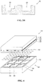
- the imprint sub mold 151 may be used for a manufacturing process of a liquid crystal panel shown in FIG. 4 .
- the liquid crystal panel may include an array substrate 250 and a color filter substrate 240 attached to each other with a liquid crystal layer 260 interposed therebetween.
- the array substrate 250 may include gate lines 256 and data lines 254 formed on an insulating substrate 252 and crossing each other.
- the array substrate 250 may further include a thin film transistor 258 at each crossing portion of the gate and data lines 256 and 254 and a pixel electrode 270 connected to the thin film transistor 258.
- the color filter substrate 240 may include color filters 246 formed on an insulating substrate 242, a black matrix 244 for partitioning the color filters 246, and a common electrode 248 forming an electric field with the pixel electrode 270 of the array substrate 250.
- the common electrode 248 may be formed on the array substrate 250.
- the thin film transistors 258, the gate lines 256, the data lines 254, and the pixel electrode 270 of the array substrate 250 may be formed through an imprint patterning process using the imprint sub mold 151. Additionally, in the liquid crystal panel, the color filters 246 and the black matrix 244 of the color filter substrate 240 may be formed through an imprint patterning process using the imprint sub mold 151.
- the imprint sub mold 151 is formed from the imprint mold 100 including the patterns of the multi-layered structure, which have improved uniformity in the height and the inclination angle of each layer, the uniformity in the heights and the inclination angles of the plurality of patterns of the liquid crystal panel, which are formed in the imprint patterning process using the imprint sub mold 151, can be improved. Therefore, the defects of the thin film patterns can be prevented from being generated in the imprint patterning process.
- the imprint mold 100 and the imprint sub mold 151 according to the present disclosure are applied to the manufacturing process of the liquid crystal panel, and the present disclosure is not limited thereto.
- the imprint mold 100 and the imprint sub mold 151 according to the present disclosure may be applied to a manufacturing process of an array substrate of an organic light emitting display device and/or may be applied to a manufacturing process of touch electrodes and touch lines of a touch display device.
- the imprint mold according to the present disclosure can prevent damages in the etching process for each layer of the patterns by forming the etch stop layer between the upper layer and the lower layer of the pattern with the multi-layered structure.
- the imprint mold can improve the height uniformity and the inclination angle uniformity of the upper and lower layers of each pattern and can prevent occurrence of the defects in the manufacturing process of the plurality of patterns of the display device using the imprint mold.
Landscapes
- Physics & Mathematics (AREA)
- General Physics & Mathematics (AREA)
- Engineering & Computer Science (AREA)
- Mechanical Engineering (AREA)
- Manufacturing & Machinery (AREA)
- Nonlinear Science (AREA)
- Chemical & Material Sciences (AREA)
- Crystallography & Structural Chemistry (AREA)
- Optics & Photonics (AREA)
- Shaping Of Tube Ends By Bending Or Straightening (AREA)
- Exposure Of Semiconductors, Excluding Electron Or Ion Beam Exposure (AREA)
Abstract
Description
- The present application claims priority to Korean Patent Application No.
10-2016-0139358 filed on October 25, 2016 - The present disclosure relates to an imprint mold having multi-layered patterns and a manufacturing method of the same.
- Liquid crystal display devices among various flat panel display devices have been widely used for display devices such as notebook computers, televisions, tablet computers, monitors, smartphones, potable display instruments and portable information instruments because of their thin thicknesses, light weights, lower power consumption.
- A liquid crystal display device includes a plurality of thin films, each of which is formed through a mask process including deposition, light-exposing, developing and etching steps. The mask process increases manufacturing costs because it is very complicated. Therefore, an imprint patterning process using an imprint mold has been researched to form the plurality of thin films of the liquid crystal display device.
- In the imprint patterning process, thin film patterns are formed by contacting an imprint mold with a resin layer coated on a substrate of the liquid crystal display device. Here, the imprint mold has a plurality of patterns opposite to the thin film patterns to be formed on the substrate, and the patterns are reversed and transferred to the resin layer, thereby forming the thin film patterns.
- The patterns of the imprint mold are formed through a mask process including light-exposing, developing and etching steps. For example, the patterns may be formed by patterning a resin layer coated on a substrate for an imprint mold through the mask process.
- However, in the imprint mold, there occur variations in heights and inclination angles of the patterns due to deviation of the mask process and a size of the pattern. As a result, defects of the thin film patterns occur in the imprint patterning process of the liquid crystal device using the imprint mold. The defects become worse when the patterns of the imprint mold each have a multi-layered structure.
- Accordingly, the present disclosure is directed to an imprint mold and a manufacturing method of the same that substantially obviate one or more of the problems due to limitations and disadvantages of the related art.
- An object of the present disclosure is to provide an imprint mold and a manufacturing method of the same capable of improving uniformity in heights and inclination angles of patterns with a multi-layered structure.
- Additional features and advantages of the disclosure will be set forth in the description which follows, and in part will be apparent from the description, or may be learned by practice of the disclosure. The objectives and other advantages of the disclosure will be realized and attained by the structure particularly pointed out in the written description and claims hereof as well as the appended drawings.
- The object is solved by the features of the independent claims. Preferred embodiments are given in the dependent claims.
- To achieve these and other advantages and in accordance with the purpose of the present disclosure, as embodied and broadly described herein, there is provided an imprint mold that includes a substrate; a pattern on the substrate and having a multi-layered structure; and an etch stop layer between an upper layer and a lower layer of the pattern.
- In another aspect, a manufacturing method of an imprint mold includes sequentially forming a buffer layer, a first resin pattern layer, an etch stop pattern layer, and a second resin pattern layer on a substrate; forming an upper layer of a pattern by selectively etching the second resin pattern layer; forming an etch stop layer under the upper layer by selectively etching the etch stop pattern layer; and forming a lower layer of the pattern under the etch stop layer by selectively etching the first resin pattern layer.
- Preferably, the pattern has a multi-stage structure in which the upper layer has a smaller size than the lower layer, and the etch stop layer has a size corresponding to an upper surface of the lower layer.
- Preferably, a buffer layer may be provided between the substrate and the lower layer.
- Preferably, a first passivation layer may be provided on the upper layer of the pattern and a second passivation layer may be provided all over the substrate including the pattern.
- Preferably, the first passivation layer and the second passivation layer are sequentially layered on the upper layer of the pattern and constitute a double-layered structure.
- Preferably, the substrate is a plastic.
- Preferably, the upper layer and/or the lower layer might be composed of a resin.
- Preferably, the substrate is a glass.
- Preferably, the etch stop layer is composed of a metal.
- Preferably, the method may further comprise forming a first passivation pattern layer all over the substrate including the upper layer of the pattern before forming the etch stop layer.
- Preferably, forming the etch stop layer may include forming a first passivation layer under the upper layer by etching the first passivation pattern layer.
- Preferably, forming a second passivation layer all over the substrate may include the pattern after forming the lower layer of the pattern.
- It is to be understood that both the foregoing general description and the following detailed description are exemplary and explanatory and are intended to provide further explanation of the disclosure as claimed.
- The accompanying drawings, which are included to provide a further understanding of the disclosure and which are incorporated in and constitute a part of this specification, illustrate embodiments of the disclosure and together with the description serve to explain the principles of the disclosure. In the drawings:
-
FIG. 1 is a schematic view of an imprint mold according to an embodiment of the present disclosure. -
FIGs. 2A to 2G are views of illustrating respective steps in a manufacturing process of an imprint mold according to the embodiment of the present disclosure. -
FIGs. 3A and3B are views of illustrating respective steps in a manufacturing process of a sub mold using an imprint mold of the present disclosure. -
FIG. 4 is a view of a liquid crystal panel having patterns formed through an imprint patterning process using an imprint mold according to the present disclosure. - Reference will now be made in detail to embodiments of the disclosure, examples of which are illustrated in the accompanying drawings.
-
FIG. 1 is a schematic view of an imprint mold according to an embodiment of the present disclosure. - In
FIG. 1 , theimprint mold 100 according to the embodiment of the present disclosure includes at least one pattern having a multi-layered structure formed on asubstrate 101. For example, theimprint mold 100 may include afirst pattern 131 and asecond pattern 133. - The
first pattern 131 may include a first-first pattern 131a as a lower layer and a first-second pattern 131b as an upper layer. The first-first pattern 131a and the first-second pattern 131b of thefirst pattern 131 may have the same size. The first-first pattern 131 a and the first-second pattern 131b of thefirst pattern 131 may also have the same height and inclination angle. - The
second pattern 133 may include a second-first pattern 133a as a lower layer and a second-second pattern 133b as an upper layer. The second-first pattern 133a and the second-second pattern 133b of thesecond pattern 133 may have different sizes, and thus, thesecond pattern 133 may have one or more steps or multiple steps, that is, a stage or multi-stage structure. Here, the second-second pattern 133b may have a smaller size than the second-first pattern 133a. The second-first pattern 133a and the second-second pattern 133b of thefirst pattern 133 may also have the same height and/or inclined angle. - An
etch stop layer 113a may be disposed between the first-first pattern 131a and the first-second pattern 131b of thefirst pattern 131. In addition, anetch stop layer 113b may be disposed between the second-first pattern 133a and the second-second pattern 133b of thesecond pattern 133. Theetch stop layers first pattern 131a and the second-first pattern 133a from being etched in respective processes of forming the upper layers of thefirst pattern 131 and thesecond pattern 133. Theetch stop layers first pattern 131 and thesecond pattern 133. - Moreover, a
buffer layer 111 may be disposed all over thesubstrate 101, and the lower layers of thefirst pattern 131 and thesecond pattern 133, that is, the first-first pattern 131a and the second-first pattern 133a may be positioned on thebuffer layer 111. So thebuffer layer 111 is positioned between thesubstrate 111 and thefirst pattern 131 and thesecond pattern 133. Thebuffer layer 111 may increase adhesion between thesubstrate 101 and the first-first pattern 131a and adhesion between thesubstrate 101 and the second-first pattern 133a. - Furthermore, at least one passivation layer may be disposed over the
first pattern 131 and thesecond pattern 133. For example,first passivation layers second passivation layer 117 may be disposed over thefirst pattern 131 and thesecond pattern 133. - The
first passivation layers first pattern 131 and thesecond pattern 133, respectively. Thesecond passivation layer 117 may be formed all over thesubstrate 101 including thefirst pattern 131 and thesecond pattern 133. Thefirst passivation layers second passivation layer 117 may protect thefirst pattern 131 and thesecond pattern 133 from be damaged. - Here, on the
first pattern 131 and thesecond pattern 133, more specifically, on the first-second pattern 131b of thefirst pattern 131 and the second-second pattern 133b of thesecond pattern 133, thefirst passivation layers second passivation layer 117 may are sequentially layered to constitute a double-layered structure. -
FIGs. 2A to 2G are views of illustrating respective steps in a manufacturing process of an imprint mold according to the embodiment of the present disclosure. - In
FIG. 2A , abuffer layer 111, a firstresin pattern layer 121, an etchstop pattern layer 113 and a secondresin pattern layer 123 may be sequentially formed all over asubstrate 101 for an imprint mold. - The
substrate 101 may be an insulating substrate such as a glass substrate or may be a flexible substrate such as a plastic film. - The
buffer layer 111 may be deposited all over thesubstrate 101. Thebuffer layer 111 may be formed of a conductive material such as indium tin oxide (ITO) and indium zinc oxide (IZO) or an inorganic material such as silicon oxide (SiO2) and silicon nitride (SiNx). Alternatively, thebuffer layer 111 may be formed of a metallic material such as molybdenum (Mo), titanium (Ti) or molybdenum/titanium (MoTi). Thebuffer layer 111 may increase the adhesion between the firstresin pattern layer 121 and thesubstrate 101 and may have a thickness of 500 to 1000 Å. - The first
resin pattern layer 121 may be coated all over thebuffer layer 111. The firstresin pattern layer 121 is used to form the lower layers of thefirst pattern 131 and thesecond pattern 133 ofFIG. 1 . The firstresin pattern layer 121 may be an organic material such as photo-curable acrylate or the like. - The etch
stop pattern layer 113 may be deposited all over the firstresin pattern layer 121. The etchstop pattern layer 113 may be an etch stopper for protecting the firstresin pattern layer 121 during a step of etching each of the upper layers of thefirst pattern 131 and thesecond pattern 133. The etchstop pattern layer 113 may be formed of a material such as ITO or IZO. The etchstop pattern layer 113 may have a thickness of 500 to 1000 Å. - The second
resin pattern layer 123 may be coated all over the etchstop pattern layer 113. The secondresin pattern layer 123 is used to form the upper layers of thefirst pattern 131 and thesecond pattern 133 ofFIG. 1 . The secondresin pattern layer 123 may be an organic material such as photo-curable acrylate or the like. - Referring to
FIGs. 2B and2C , first photo resistpatterns 141 may be formed by applying photoresist (not shown) all over the secondresin pattern layer 123 and selectively patterning it. - Then, the second
resin pattern layer 123 may be selectively etched by using thefirst photoresist patterns 141 as an etching mask, thereby forming the upper layers of thefirst pattern 131 and thesecond pattern 133, that is, the first-second pattern 131b and the second-second pattern 133b. Here, the secondresin pattern layer 123 may be dry-etched. At this time, since the etchstop pattern layer 113 is positioned between the firstresin pattern layer 121 and the secondresin pattern layer 123, only the secondresin pattern layer 123 may be etched in the above-mentioned etching step. - Subsequently, the
first photoresist patterns 141 remaining on thesubstrate 101 may be removed through an ashing process, and a firstpassivation pattern layer 115 may be deposited all over thesubstrate 101 including the first-second pattern 131b and the second-second pattern 133b. The firstpassivation pattern layer 115 may be formed of ITO or IZO and may have a thickness of 100 to 500 Å. - Next, in
FIG. 2D ,second photoresist patterns 143 may be formed by applying photoresist (not shown) all over the firstpassivation pattern layer 115 and selectively patterning it. - Then, referring to
FIGs. 2E and2F , the firstpassivation pattern layer 115 and the etchstop pattern layer 113 may be selectively etched in order by using thesecond photoresist patterns 143 as an etching mask, thereby forming thefirst passivation layers etch stop layers passivation pattern layer 115 and the etchstop pattern layer 113 may be wet-etched. - Since the
second photoresist patterns 143 are used for the above-mentioned etching step, the firstpassivation pattern layer 115 and the etchstop pattern layer 113 may be etched in all regions except a region overlapping thesecond photoresist patterns 143. Therefore, thefirst passivation layer 115b on the second-second pattern 133b and theetch stop layer 113b under the second-second pattern 133b have a larger area than the second-second pattern 133b. Namely, theetch stop layers first pattern 131 and thesecond pattern 133, respectively. - Subsequently, the first
resin pattern layer 121 may be selectively etched by using thesecond photoresist patterns 143 as an etching mask, thereby forming the lower layers of thefirst pattern 131 and thesecond pattern 133, that is, the first-first pattern 131 a and the second-first pattern 133a. The firstresin pattern layer 121 may be dry-etched. - Then, in
FIG. 2G , thesecond passivation layer 117 may be formed by depositing a second passivation pattern layer all over thesubstrate 101 on which thefirst pattern 131 and thesecond pattern 133 are formed. Thesecond passivation layer 117 may be formed of ITO or IZO and may have a thickness of 100 to 500 Å. - The
imprint mold 100 including thefirst pattern 131 and thesecond pattern 133 of the multiple-layered structure may be formed on thesubstrate 101 through the above-mentioned processes. Here, thesecond pattern 133 may have the multi-stage structure in which the upper layer has a smaller area than the lower layer, i.e., the second-second pattern 133b has a smaller layer than the second-first pattern 133a. - As stated above, in the
imprint mold 100 according to the embodiment of the present disclosure, theetch stop layer 113a is disposed between the upper layer and the lower layer of thefirst pattern 131, and theetch stop layer 113b is disposed between the upper layer and the lower layer of thesecond pattern 133. Theetch stop layers substrate 101 from being damaged during the etching steps. Accordingly, it is possible to improve uniformity in heights and inclination angles of the patterns with a multi-layered structure of theimprint mold 100. For example, in theimprint mold 100, the height and the inclination angle between the first-first pattern 131a and the first-second pattern 131b of thefirst pattern 131 may be substantially equal to the height and the inclination angle between the second-first pattern 133a and the second-second pattern 133b of thesecond pattern 133 within an error range due to theetch stop layers - Meanwhile, in the etching step of the first
passivation pattern layer 115 and the etchstop pattern layer 113, thefirst passivation layers second pattern 131b and the second-second pattern 133b. Thus, a double layer of thefirst passivation layer 115a and thesecond passivation layer 117 may be formed on thefirst pattern 131, and a double layer of thefirst passivation layer 115b and thesecond passivation layer 117 may be formed on thesecond pattern 133. -
FIGs. 3A and3B are views of illustrating respective steps in a manufacturing process of a sub mold using an imprint mold of the present disclosure. - The imprint mold of the present disclosure, which is explained with reference to
FIG. 1 andFIGs. 2A to 2G , is an imprint master mold. The imprint master mold includes multi-stage patterns substantially the same as thin film patterns to be formed in the display device. Accordingly, a mold having multi-stage patterns opposite to the thin film patterns of the display device is needed in order to perform an imprint patterning process to the display device. Hereinafter, an imprint sub mold used in the imprint patterning process of the display device will be described. - Referring to
FIG. 3A , apolymer material 150 having a rubber property may be applied to theimprint mold 100 ofFIG. 1 according to the present disclosure and may be thermally cured or photo-cured. Thepolymer material 150 may be formed of polydimethylsiloxane (PDMS) or the like. - According to this, the
first pattern 131 and thesecond pattern 133 of theimprint mold 100 may be reversed and transferred to thepolymer material 150, and thusimprint sub mold 151 may be formed as shown inFIG. 3B . - The
imprint sub mold 151 may include a first dentedportion 152 and a second dentedportion 153. The first dentedportion 152 may correspond to thefirst pattern 131 of theimprint mold 100, and the second dentedportion 153 may correspond to thesecond pattern 133. - The
imprint sub mold 151 may form mask patterns with multiple steps for patterning the thin film patterns of an array substrate of various display devices, for example, a liquid crystal display device, an electrophoretic display device, an organic light-emitting display device or the like. - For instance, the
imprint sub mold 151 may be used for a manufacturing process of a liquid crystal panel shown inFIG. 4 . Specifically, the liquid crystal panel may include anarray substrate 250 and acolor filter substrate 240 attached to each other with aliquid crystal layer 260 interposed therebetween. - The
array substrate 250 may includegate lines 256 anddata lines 254 formed on an insulatingsubstrate 252 and crossing each other. Thearray substrate 250 may further include athin film transistor 258 at each crossing portion of the gate anddata lines pixel electrode 270 connected to thethin film transistor 258. - The
color filter substrate 240 may includecolor filters 246 formed on an insulatingsubstrate 242, ablack matrix 244 for partitioning thecolor filters 246, and acommon electrode 248 forming an electric field with thepixel electrode 270 of thearray substrate 250. Thecommon electrode 248 may be formed on thearray substrate 250. - In the liquid crystal panel, the
thin film transistors 258, thegate lines 256, thedata lines 254, and thepixel electrode 270 of thearray substrate 250 may be formed through an imprint patterning process using theimprint sub mold 151. Additionally, in the liquid crystal panel, thecolor filters 246 and theblack matrix 244 of thecolor filter substrate 240 may be formed through an imprint patterning process using theimprint sub mold 151. - Here, since the
imprint sub mold 151 is formed from theimprint mold 100 including the patterns of the multi-layered structure, which have improved uniformity in the height and the inclination angle of each layer, the uniformity in the heights and the inclination angles of the plurality of patterns of the liquid crystal panel, which are formed in the imprint patterning process using theimprint sub mold 151, can be improved. Therefore, the defects of the thin film patterns can be prevented from being generated in the imprint patterning process. - In the meantime, the
imprint mold 100 and theimprint sub mold 151 according to the present disclosure are applied to the manufacturing process of the liquid crystal panel, and the present disclosure is not limited thereto. For example, theimprint mold 100 and theimprint sub mold 151 according to the present disclosure may be applied to a manufacturing process of an array substrate of an organic light emitting display device and/or may be applied to a manufacturing process of touch electrodes and touch lines of a touch display device. - The imprint mold according to the present disclosure can prevent damages in the etching process for each layer of the patterns by forming the etch stop layer between the upper layer and the lower layer of the pattern with the multi-layered structure.
- Accordingly, the imprint mold can improve the height uniformity and the inclination angle uniformity of the upper and lower layers of each pattern and can prevent occurrence of the defects in the manufacturing process of the plurality of patterns of the display device using the imprint mold.
- It will be apparent to those skilled in the art that various modifications and variations can be made in a display device of the present disclosure without departing from the scope of the embodiments. Thus, it is intended that the present disclosure covers the modifications and variations of this disclosure provided they come within the scope of the appended claims and their equivalents.
- The various embodiments described above can be combined to provide further embodiments. Aspects of the embodiments can be modified, if necessary to employ concepts of the various patents, applications and publications to provide yet further embodiments.
- These and other changes can be made to the embodiments in light of the above-detailed description. In general, in the following claims, the terms used should not be construed to limit the claims to the specific embodiments disclosed in the specification and the claims, but should be construed to include all possible embodiments along with the full scope of equivalents to which such claims are entitled. Accordingly, the claims are not limited by the disclosure.
Claims (13)
- An imprint mold comprising:a substrate (101) of the imprint mold (100);a pattern (131, 133) on the substrate (101), the pattern having a multi-layered structure; andan etch stop layer (113a, 113b) between an upper layer (131a, 133a) and a lower layer (131b, 133b) of the pattern.
- The imprint mold of claim 1, wherein the pattern (133) has a multi-stage structure in which the upper layer (133b) has a smaller size than the lower layer (133a), and the etch stop layer (113b) has a size corresponding to an upper surface of the lower layer (133b).
- The imprint mold of claim 1 or 2, further comprising a buffer layer (111) between the substrate (101) and the pattern (131, 133).
- The imprint mold of any one of the claims 2 or 3, further comprising a first passivation layer (115a, 115b) on the upper layer (131b, 133b) of the pattern (131, 133) and/or a second passivation layer (117) all over the substrate (101) including the pattern (131, 133).
- The imprint mold of claim 4, wherein the first passivation layer (115a, 115b) and the second passivation layer (177) are sequentially layered on the upper layer (131b, 133b) of the pattern (131, 133) and constitute a double-layered structure.
- The imprint mold of any one of the preceding claims, wherein the substrate (101) is a plastic or a glass.
- The imprint mold of any one of the preceding claims, wherein the upper layer (131b, 133b) is composed of a resin and/ or the lower layer (131a 133a) is composed of a resin.
- The imprint mold any one of the preceding claims, wherein the etch stop layer (113a, 113b) is composed of a metal.
- A manufacturing method of an imprint mold comprising:sequentially forming a buffer layer (111), a first resin pattern layer (121), an etch stop pattern layer (113), and a second resin pattern layer (123) on a substrate (101);forming an upper layer (131b, 133b) of a pattern by selectively etching the second resin pattern layer (123);forming an etch stop layer (113a, 113b) under the upper layer (131b, 133b) by selectively etching the etch stop pattern layer (113); andforming a lower layer (131a, 133a) of the pattern under the etch stop layer (113a, 113b) by selectively etching the first resin pattern layer (121).
- The method of claim 9, further comprising: forming a first passivation pattern layer (115) all over the substrate (101) including the upper layer (131b, 133b) of the pattern before forming the etch stop layer (113a, 113b),
wherein forming the etch stop layer (113a, 113b) includes forming a first passivation layer (115a, 115b) over the upper layer (131b, 133b) by etching the first passivation pattern layer (115a, 115b). - The method of claim 10, further comprising: forming a second passivation layer (117) all over the substrate (101) including the pattern (131, 133) after forming the lower layer (131a, 133a) of the pattern.
- Use of the imprint mold (100) as defined in any one of the claims 1-8 for forming an imprint sub mold (151), wherein the imprint sub mold (151) includes a first dented portion (152) corresponding to the first pattern (131) of the imprint mold (100) and a second dented portion (153) corresponding to the second pattern (133) of the imprint mold (100).
- Use of the imprint mold (100) and the imprint sub mold (151) as claimed in any one of the preceding claims for manufacturing of an array substrate of an organic light emitting display device or for manufacturing of touch electrodes and touch lines of a touch display device.
Applications Claiming Priority (1)
| Application Number | Priority Date | Filing Date | Title |
|---|---|---|---|
| KR1020160139358A KR102710915B1 (en) | 2016-10-25 | 2016-10-25 | Imprint mold and manufacturing method thereof |
Publications (2)
| Publication Number | Publication Date |
|---|---|
| EP3316035A2 true EP3316035A2 (en) | 2018-05-02 |
| EP3316035A3 EP3316035A3 (en) | 2018-07-25 |
Family
ID=60190612
Family Applications (1)
| Application Number | Title | Priority Date | Filing Date |
|---|---|---|---|
| EP17198152.5A Withdrawn EP3316035A3 (en) | 2016-10-25 | 2017-10-24 | Imprint mold and manufacturing method of the same |
Country Status (4)
| Country | Link |
|---|---|
| US (1) | US10583586B2 (en) |
| EP (1) | EP3316035A3 (en) |
| KR (1) | KR102710915B1 (en) |
| CN (1) | CN107976864B (en) |
Families Citing this family (3)
| Publication number | Priority date | Publication date | Assignee | Title |
|---|---|---|---|---|
| US10991582B2 (en) * | 2016-12-21 | 2021-04-27 | Canon Kabushiki Kaisha | Template for imprint lithography including a recession, an apparatus of using the template, and a method of fabricating an article |
| CN110494804B (en) * | 2019-07-11 | 2024-03-26 | 京东方科技集团股份有限公司 | Nanoimprint mold, method of manufacturing the same, and pattern transfer method using the nanoimprint mold |
| JP2021119375A (en) * | 2020-01-30 | 2021-08-12 | 株式会社ジャパンディスプレイ | Display device and manufacturing method for semiconductor device |
Citations (3)
| Publication number | Priority date | Publication date | Assignee | Title |
|---|---|---|---|---|
| JPH03100942A (en) * | 1989-09-13 | 1991-04-25 | Hitachi Chem Co Ltd | Production of stamper for optical disk |
| WO2009046954A2 (en) * | 2007-10-05 | 2009-04-16 | Opsolution Nanophotonics Gmbh | Method and arrangement for the production of nano-imprint stamps and micromechanically tunable filter/detector array |
| KR20110070271A (en) * | 2009-12-18 | 2011-06-24 | 엘지디스플레이 주식회사 | Imprint master mold and its manufacturing method |
Family Cites Families (14)
| Publication number | Priority date | Publication date | Assignee | Title |
|---|---|---|---|---|
| US7037639B2 (en) * | 2002-05-01 | 2006-05-02 | Molecular Imprints, Inc. | Methods of manufacturing a lithography template |
| US7063919B2 (en) * | 2002-07-31 | 2006-06-20 | Mancini David P | Lithographic template having a repaired gap defect method of repair and use |
| JP3821069B2 (en) * | 2002-08-01 | 2006-09-13 | 株式会社日立製作所 | Method for forming structure by transfer pattern |
| US7435074B2 (en) * | 2004-03-13 | 2008-10-14 | International Business Machines Corporation | Method for fabricating dual damascence structures using photo-imprint lithography, methods for fabricating imprint lithography molds for dual damascene structures, materials for imprintable dielectrics and equipment for photo-imprint lithography used in dual damascence patterning |
| CN101505974A (en) * | 2005-09-07 | 2009-08-12 | 凸版光掩膜公司 | Photomask for the fabrication of a dual damascene structure and method for forming the same |
| US7846345B2 (en) * | 2007-01-31 | 2010-12-07 | United Microelectronics Corp. | Method of manufacturing an imprinting template using a semiconductor manufacturing process and the imprinting template obtained |
| CN101943963A (en) * | 2009-07-08 | 2011-01-12 | 群康科技(深圳)有限公司 | Conducting plate and touch screen using same |
| US8499810B2 (en) * | 2009-08-27 | 2013-08-06 | Transfer Devices Inc. | Molecular transfer lithography apparatus and method for transferring patterned materials to a substrate |
| KR101595461B1 (en) * | 2009-09-08 | 2016-02-29 | 엘지디스플레이 주식회사 | Manufacturing method of imprint mold and manufacturing method of liquid crystal display panel using the imprint mold |
| JP5879086B2 (en) * | 2011-10-14 | 2016-03-08 | 国立大学法人東北大学 | Replica mold for nanoimprint |
| JP2015049282A (en) * | 2013-08-30 | 2015-03-16 | Hoya株式会社 | Photomask for manufacturing a display device, manufacturing method of photomask, pattern transfer method, and manufacturing method of display device |
| KR102084397B1 (en) * | 2013-11-04 | 2020-03-04 | 엘지디스플레이 주식회사 | Manufacturing method of liquid crystal display device |
| JP6106579B2 (en) * | 2013-11-25 | 2017-04-05 | Hoya株式会社 | Photomask manufacturing method, photomask and pattern transfer method |
| KR101593601B1 (en) * | 2014-04-03 | 2016-02-15 | 한국전자통신연구원 | A base mold and method of fabricating a mold |
-
2016
- 2016-10-25 KR KR1020160139358A patent/KR102710915B1/en active Active
-
2017
- 2017-10-24 EP EP17198152.5A patent/EP3316035A3/en not_active Withdrawn
- 2017-10-25 US US15/793,784 patent/US10583586B2/en active Active
- 2017-10-25 CN CN201711013448.7A patent/CN107976864B/en active Active
Patent Citations (3)
| Publication number | Priority date | Publication date | Assignee | Title |
|---|---|---|---|---|
| JPH03100942A (en) * | 1989-09-13 | 1991-04-25 | Hitachi Chem Co Ltd | Production of stamper for optical disk |
| WO2009046954A2 (en) * | 2007-10-05 | 2009-04-16 | Opsolution Nanophotonics Gmbh | Method and arrangement for the production of nano-imprint stamps and micromechanically tunable filter/detector array |
| KR20110070271A (en) * | 2009-12-18 | 2011-06-24 | 엘지디스플레이 주식회사 | Imprint master mold and its manufacturing method |
Also Published As
| Publication number | Publication date |
|---|---|
| KR102710915B1 (en) | 2024-09-26 |
| KR20180045354A (en) | 2018-05-04 |
| CN107976864B (en) | 2021-01-26 |
| CN107976864A (en) | 2018-05-01 |
| US10583586B2 (en) | 2020-03-10 |
| EP3316035A3 (en) | 2018-07-25 |
| US20180111291A1 (en) | 2018-04-26 |
Similar Documents
| Publication | Publication Date | Title |
|---|---|---|
| TWI553837B (en) | Method of making a display panel | |
| CN104298040B (en) | A kind of COA substrates and preparation method thereof and display device | |
| CN101261961B (en) | Manufacturing method of thin film transistor substrate | |
| KR101137865B1 (en) | Fabricating method for thin flim transister substrate and thin flim transister substrate using the same | |
| US7790532B2 (en) | Method of manufacturing thin film transistor substrate | |
| US9897863B2 (en) | Array substrate, display panel and display apparatus having recesses on data lines or gate lines | |
| CN107526224B (en) | Display device | |
| CN105158980B (en) | Liquid crystal display panel and liquid crystal display device comprising same | |
| CN107037627A (en) | A kind of polaroid and preparation method thereof, display device | |
| US20170293384A1 (en) | Display device and manufacturing method of the same | |
| US10583586B2 (en) | Imprint mold and manufacturing method of the same | |
| US20130210201A1 (en) | Method for manufacturing active array substrate | |
| US20140206139A1 (en) | Methods for fabricating a thin film transistor and an array substrate | |
| CN104465652B (en) | Array substrate, display device and manufacturing method of array substrate | |
| TWI518418B (en) | Liquid crystal display panel and liquid crystal display device containing the same | |
| CN101097924A (en) | Thin film transistor array substrate and manufacturing method thereof | |
| US20120241746A1 (en) | Electrophoresis display and manufacturing method | |
| CN108470718A (en) | Array substrate and its manufacturing method, display panel, display device | |
| US11049888B1 (en) | Manufacturing method for TFT array substrate | |
| CN105789121A (en) | Total reflection array substrate and preparation method thereof and display device | |
| EP3355346B1 (en) | Manufacturing method of array substrate, array substrate, and display device | |
| US8508678B2 (en) | Liquid crystal display device, touch panel, and display device including the same | |
| US20150187802A1 (en) | Display device and method of fabricating the same | |
| CN106449654B (en) | A kind of substrate and its preparation method, display device | |
| KR20160060223A (en) | Method of forming a fine pattern |
Legal Events
| Date | Code | Title | Description |
|---|---|---|---|
| PUAI | Public reference made under article 153(3) epc to a published international application that has entered the european phase |
Free format text: ORIGINAL CODE: 0009012 |
|
| STAA | Information on the status of an ep patent application or granted ep patent |
Free format text: STATUS: REQUEST FOR EXAMINATION WAS MADE |
|
| 17P | Request for examination filed |
Effective date: 20171024 |
|
| AK | Designated contracting states |
Kind code of ref document: A2 Designated state(s): AL AT BE BG CH CY CZ DE DK EE ES FI FR GB GR HR HU IE IS IT LI LT LU LV MC MK MT NL NO PL PT RO RS SE SI SK SM TR |
|
| AX | Request for extension of the european patent |
Extension state: BA ME |
|
| PUAL | Search report despatched |
Free format text: ORIGINAL CODE: 0009013 |
|
| AK | Designated contracting states |
Kind code of ref document: A3 Designated state(s): AL AT BE BG CH CY CZ DE DK EE ES FI FR GB GR HR HU IE IS IT LI LT LU LV MC MK MT NL NO PL PT RO RS SE SI SK SM TR |
|
| AX | Request for extension of the european patent |
Extension state: BA ME |
|
| RIC1 | Information provided on ipc code assigned before grant |
Ipc: G03F 7/00 20060101AFI20180618BHEP |
|
| RBV | Designated contracting states (corrected) |
Designated state(s): AL AT BE BG CH CY CZ DE DK EE ES FI FR GB GR HR HU IE IS IT LI LT LU LV MC MK MT NL NO PL PT RO RS SE SI SK SM TR |
|
| R17P | Request for examination filed (corrected) |
Effective date: 20171024 |
|
| STAA | Information on the status of an ep patent application or granted ep patent |
Free format text: STATUS: EXAMINATION IS IN PROGRESS |
|
| 17Q | First examination report despatched |
Effective date: 20210716 |
|
| STAA | Information on the status of an ep patent application or granted ep patent |
Free format text: STATUS: THE APPLICATION IS DEEMED TO BE WITHDRAWN |
|
| 18D | Application deemed to be withdrawn |
Effective date: 20230927 |