EP3315952A1 - Surface flaw detection method, surface flaw detection device, and manufacturing method for steel material - Google Patents
Surface flaw detection method, surface flaw detection device, and manufacturing method for steel material Download PDFInfo
- Publication number
- EP3315952A1 EP3315952A1 EP16814396.4A EP16814396A EP3315952A1 EP 3315952 A1 EP3315952 A1 EP 3315952A1 EP 16814396 A EP16814396 A EP 16814396A EP 3315952 A1 EP3315952 A1 EP 3315952A1
- Authority
- EP
- European Patent Office
- Prior art keywords
- surface defect
- light
- illumination lights
- light sources
- inspection target
- Prior art date
- Legal status (The legal status is an assumption and is not a legal conclusion. Google has not performed a legal analysis and makes no representation as to the accuracy of the status listed.)
- Withdrawn
Links
- 238000001514 detection method Methods 0.000 title claims abstract description 84
- 229910000831 Steel Inorganic materials 0.000 title claims abstract description 72
- 239000010959 steel Substances 0.000 title claims abstract description 72
- 238000004519 manufacturing process Methods 0.000 title claims description 17
- 239000000463 material Substances 0.000 title 1
- 230000007547 defect Effects 0.000 claims abstract description 203
- 238000005286 illumination Methods 0.000 claims abstract description 135
- 238000012545 processing Methods 0.000 claims abstract description 94
- 238000007689 inspection Methods 0.000 claims abstract description 61
- 238000000034 method Methods 0.000 claims abstract description 27
- 230000001678 irradiating effect Effects 0.000 claims abstract description 14
- 239000000047 product Substances 0.000 description 38
- 238000010586 diagram Methods 0.000 description 37
- 239000013598 vector Substances 0.000 description 33
- 230000003287 optical effect Effects 0.000 description 20
- 238000012986 modification Methods 0.000 description 16
- 230000004048 modification Effects 0.000 description 16
- 230000008859 change Effects 0.000 description 14
- 238000003384 imaging method Methods 0.000 description 12
- 238000004364 calculation method Methods 0.000 description 10
- 238000003705 background correction Methods 0.000 description 9
- 238000002474 experimental method Methods 0.000 description 7
- 230000007423 decrease Effects 0.000 description 6
- 238000011156 evaluation Methods 0.000 description 5
- XEEYBQQBJWHFJM-UHFFFAOYSA-N Iron Chemical compound [Fe] XEEYBQQBJWHFJM-UHFFFAOYSA-N 0.000 description 4
- 239000000284 extract Substances 0.000 description 4
- 230000010287 polarization Effects 0.000 description 4
- 230000001419 dependent effect Effects 0.000 description 3
- 238000002372 labelling Methods 0.000 description 3
- 230000005540 biological transmission Effects 0.000 description 2
- 230000000694 effects Effects 0.000 description 2
- 229910052742 iron Inorganic materials 0.000 description 2
- 238000012552 review Methods 0.000 description 2
- 230000003746 surface roughness Effects 0.000 description 2
- 238000012935 Averaging Methods 0.000 description 1
- 238000004458 analytical method Methods 0.000 description 1
- 230000002238 attenuated effect Effects 0.000 description 1
- 230000002146 bilateral effect Effects 0.000 description 1
- 239000010960 cold rolled steel Substances 0.000 description 1
- 230000008602 contraction Effects 0.000 description 1
- 230000003247 decreasing effect Effects 0.000 description 1
- 238000009795 derivation Methods 0.000 description 1
- 238000009792 diffusion process Methods 0.000 description 1
- 238000009826 distribution Methods 0.000 description 1
- 238000000605 extraction Methods 0.000 description 1
- 238000001914 filtration Methods 0.000 description 1
- 230000010365 information processing Effects 0.000 description 1
- 238000009533 lab test Methods 0.000 description 1
- LKACJLUUJRMGFK-UHFFFAOYSA-N methylsulfonal Chemical compound CCS(=O)(=O)C(C)(CC)S(=O)(=O)CC LKACJLUUJRMGFK-UHFFFAOYSA-N 0.000 description 1
- 238000013041 optical simulation Methods 0.000 description 1
- 230000008569 process Effects 0.000 description 1
- 230000009467 reduction Effects 0.000 description 1
- 238000002310 reflectometry Methods 0.000 description 1
- 238000011160 research Methods 0.000 description 1
- 239000011265 semifinished product Substances 0.000 description 1
- 238000004088 simulation Methods 0.000 description 1
- 238000003892 spreading Methods 0.000 description 1
- 230000007480 spreading Effects 0.000 description 1
- 238000005482 strain hardening Methods 0.000 description 1
- 230000001360 synchronised effect Effects 0.000 description 1
- 238000012360 testing method Methods 0.000 description 1
Images









Classifications
-
- G—PHYSICS
- G01—MEASURING; TESTING
- G01N—INVESTIGATING OR ANALYSING MATERIALS BY DETERMINING THEIR CHEMICAL OR PHYSICAL PROPERTIES
- G01N21/00—Investigating or analysing materials by the use of optical means, i.e. using sub-millimetre waves, infrared, visible or ultraviolet light
- G01N21/84—Systems specially adapted for particular applications
- G01N21/88—Investigating the presence of flaws or contamination
- G01N21/89—Investigating the presence of flaws or contamination in moving material, e.g. running paper or textiles
- G01N21/892—Investigating the presence of flaws or contamination in moving material, e.g. running paper or textiles characterised by the flaw, defect or object feature examined
-
- G—PHYSICS
- G01—MEASURING; TESTING
- G01N—INVESTIGATING OR ANALYSING MATERIALS BY DETERMINING THEIR CHEMICAL OR PHYSICAL PROPERTIES
- G01N21/00—Investigating or analysing materials by the use of optical means, i.e. using sub-millimetre waves, infrared, visible or ultraviolet light
- G01N21/84—Systems specially adapted for particular applications
- G01N21/88—Investigating the presence of flaws or contamination
- G01N21/8806—Specially adapted optical and illumination features
-
- G—PHYSICS
- G01—MEASURING; TESTING
- G01N—INVESTIGATING OR ANALYSING MATERIALS BY DETERMINING THEIR CHEMICAL OR PHYSICAL PROPERTIES
- G01N21/00—Investigating or analysing materials by the use of optical means, i.e. using sub-millimetre waves, infrared, visible or ultraviolet light
- G01N21/84—Systems specially adapted for particular applications
- G01N21/88—Investigating the presence of flaws or contamination
- G01N21/89—Investigating the presence of flaws or contamination in moving material, e.g. running paper or textiles
- G01N21/8901—Optical details; Scanning details
-
- G—PHYSICS
- G01—MEASURING; TESTING
- G01N—INVESTIGATING OR ANALYSING MATERIALS BY DETERMINING THEIR CHEMICAL OR PHYSICAL PROPERTIES
- G01N21/00—Investigating or analysing materials by the use of optical means, i.e. using sub-millimetre waves, infrared, visible or ultraviolet light
- G01N21/84—Systems specially adapted for particular applications
- G01N21/88—Investigating the presence of flaws or contamination
- G01N21/95—Investigating the presence of flaws or contamination characterised by the material or shape of the object to be examined
- G01N21/956—Inspecting patterns on the surface of objects
- G01N21/95607—Inspecting patterns on the surface of objects using a comparative method
-
- G—PHYSICS
- G01—MEASURING; TESTING
- G01N—INVESTIGATING OR ANALYSING MATERIALS BY DETERMINING THEIR CHEMICAL OR PHYSICAL PROPERTIES
- G01N21/00—Investigating or analysing materials by the use of optical means, i.e. using sub-millimetre waves, infrared, visible or ultraviolet light
- G01N21/84—Systems specially adapted for particular applications
- G01N21/88—Investigating the presence of flaws or contamination
- G01N21/8806—Specially adapted optical and illumination features
- G01N2021/8809—Adjustment for highlighting flaws
-
- G—PHYSICS
- G01—MEASURING; TESTING
- G01N—INVESTIGATING OR ANALYSING MATERIALS BY DETERMINING THEIR CHEMICAL OR PHYSICAL PROPERTIES
- G01N21/00—Investigating or analysing materials by the use of optical means, i.e. using sub-millimetre waves, infrared, visible or ultraviolet light
- G01N21/84—Systems specially adapted for particular applications
- G01N21/88—Investigating the presence of flaws or contamination
- G01N21/8806—Specially adapted optical and illumination features
- G01N2021/8812—Diffuse illumination, e.g. "sky"
- G01N2021/8816—Diffuse illumination, e.g. "sky" by using multiple sources, e.g. LEDs
-
- G—PHYSICS
- G01—MEASURING; TESTING
- G01N—INVESTIGATING OR ANALYSING MATERIALS BY DETERMINING THEIR CHEMICAL OR PHYSICAL PROPERTIES
- G01N21/00—Investigating or analysing materials by the use of optical means, i.e. using sub-millimetre waves, infrared, visible or ultraviolet light
- G01N21/84—Systems specially adapted for particular applications
- G01N21/88—Investigating the presence of flaws or contamination
- G01N21/8851—Scan or image signal processing specially adapted therefor, e.g. for scan signal adjustment, for detecting different kinds of defects, for compensating for structures, markings, edges
- G01N2021/8887—Scan or image signal processing specially adapted therefor, e.g. for scan signal adjustment, for detecting different kinds of defects, for compensating for structures, markings, edges based on image processing techniques
-
- G—PHYSICS
- G01—MEASURING; TESTING
- G01N—INVESTIGATING OR ANALYSING MATERIALS BY DETERMINING THEIR CHEMICAL OR PHYSICAL PROPERTIES
- G01N21/00—Investigating or analysing materials by the use of optical means, i.e. using sub-millimetre waves, infrared, visible or ultraviolet light
- G01N21/84—Systems specially adapted for particular applications
- G01N21/88—Investigating the presence of flaws or contamination
- G01N21/89—Investigating the presence of flaws or contamination in moving material, e.g. running paper or textiles
- G01N21/8914—Investigating the presence of flaws or contamination in moving material, e.g. running paper or textiles characterised by the material examined
- G01N2021/8918—Metal
-
- G—PHYSICS
- G01—MEASURING; TESTING
- G01N—INVESTIGATING OR ANALYSING MATERIALS BY DETERMINING THEIR CHEMICAL OR PHYSICAL PROPERTIES
- G01N21/00—Investigating or analysing materials by the use of optical means, i.e. using sub-millimetre waves, infrared, visible or ultraviolet light
- G01N21/84—Systems specially adapted for particular applications
- G01N21/88—Investigating the presence of flaws or contamination
- G01N21/89—Investigating the presence of flaws or contamination in moving material, e.g. running paper or textiles
- G01N21/892—Investigating the presence of flaws or contamination in moving material, e.g. running paper or textiles characterised by the flaw, defect or object feature examined
- G01N2021/8924—Dents; Relief flaws
-
- G—PHYSICS
- G01—MEASURING; TESTING
- G01N—INVESTIGATING OR ANALYSING MATERIALS BY DETERMINING THEIR CHEMICAL OR PHYSICAL PROPERTIES
- G01N21/00—Investigating or analysing materials by the use of optical means, i.e. using sub-millimetre waves, infrared, visible or ultraviolet light
- G01N21/84—Systems specially adapted for particular applications
- G01N21/88—Investigating the presence of flaws or contamination
- G01N21/95—Investigating the presence of flaws or contamination characterised by the material or shape of the object to be examined
- G01N21/952—Inspecting the exterior surface of cylindrical bodies or wires
Definitions
- the present invention relates to a surface defect detection method and a surface defect detection device that optically detect surface defects of a steel product, and to a method for manufacturing a steel product, the method detecting surface defects of the steel product using the surface defect detection method, and manufacturing the steel product on the basis of the detection results.
- steel product refers to an article of iron or steel, such a steel sheet or a shaped steel, including, for example, a seamless steel pipe, a welded steel pipe, a hot-rolled steel sheet, a cold-rolled steel sheet, and a thick plate, and to a semifinished product, such as a slab, produced in the process of manufacturing the article of iron or steel.
- a method has also been developed in which visible light beams in a plurality of wavelength regions that neither affect nor are affected by self-emitting light emitted from a hot steel product and do not affect each other are emitted from mutually symmetrical directions oblique to a normal line to the surface of the hot steel product, an image formed by combined reflected light beams and images formed by the individual reflected light beams are obtained in the normal direction to the surface of the hot steel product, and a surface defect of the hot steel product is detected from a combination of these images (refer to Patent Literature 2).
- the method described in Patent Literature 1 since harmless patterns and scale have different reflectance from that of a base steel portion, the sound harmless patterns or scale may be erroneously detected as the surface defects. For this reason, in the method described in Patent Literature 1, the billet is distinguished from the scale using the fact that the shape of the billet is linear. However, the surface defects of a steel product have not only linear shapes, but also various shapes, such as circular shapes. Therefore, the method described in Patent Literature 1 is difficult to be applied to the detection processing for the surface defects of the steel product. In the method described in Patent Literature 2, since a large number of types of surface defects, scale, harmless patterns and the like are present, simply combining the images is difficult to distinguish the surface defects from the scale or the harmless patterns. In addition, detection logic for dealing with a combination of a large number of images is realistically difficult to be established.
- a surface defect detection method of optically detecting a surface defect of a steel product includes: an irradiating step of irradiating illumination lights from different directions to an identical inspection target portion by using at least two distinguishable light sources; and a detecting step of acquiring images by reflection lights of the respective illumination lights and detecting a surface defect in the inspection target portion by performing difference processing between the acquired images, wherein an incident angle of the illumination lights of the respective light sources are within a range of 60° to 82.5° relative to the inspection target portion.
- the irradiating step includes a step of irradiating illumination lights by causing at least two flash light sources to emit light repeatedly such that light emission timing does not synchronize with each other, and/or a step of irradiating illumination lights of light sources, wavelength regions of which do not overlap with each other, and when the illumination lights of the light sources having the wavelength regions not overlapping one another are irradiated simultaneously, the detecting step includes a step of acquiring an image by a reflection light of each of the illumination lights by separating reflection lights of the respective mixed illumination lights by using filters that pass light having a wavelength identical to a wavelength of the illumination lights.
- the detecting step includes a first determining step of extracting a bright portion and a dark portion of an image that has been acquired by performing difference processing on the acquired images, and of determining whether a concavo-convex surface defect is present based on a positional relationship between the extracted bright portion and dark portion, and an irradiation directions of the illumination lights.
- a method for manufacturing a steel product according to the present invention includes: a step of detecting a surface defect of a steel product by using the surface defect detection method according to the present invention; and of manufacturing a steel product based on a result of detection.
- a surface defect detection method and a surface defect detection device can accurately distinguish scale or harmless patterns from surface defects.
- a method for manufacturing a steel product according to the present invention enables the accurate distinction of the scale or the harmless patterns from the surface defects, and enables manufacturing of the steel product on the basis of the distinction result.
- FIG. 1 is a schematic diagram showing a configuration of a surface defect detection device of a first embodiment of the present invention.
- a surface defect detection device 1 of the first embodiment of the present invention is a device that detects a surface defect of a steel pipe P in a cylindrical shape that is conveyed in a direction of an arrow in the figure, and that includes light sources 2a, 2b, a function generator 3, area sensors 4a, 4b, an image processing device 5, and a monitor 6 as main components.
- the light sources 2a, 2b irradiate a distinguishable illumination light L at an identical inspection target portion on a surface of the steel pipe P, in accordance with a trigger signal from the function generator 3. It is desirable that the light sources 2a, 2b be arranged symmetrically with respect to the inspection target portion. Therefore, the light sources 2a, 2b are arranged so as to be shifted by an identical angle relative to the normal vector of the surface of the steel pipe P so that an irradiation direction vector of the illumination light L and the normal vector of the surface of the steel pipe P are on the same plane.
- the identity of incident angle described herein aims to equalize optical conditions as much as possible when the light sources in different directions are distinguished, and to suppress a signal of a sound portion including a scale and a harmless pattern significantly by difference processing. Moreover, as a signal of a sound portion is greatly dependent on a surface condition of a target, it is difficult to guarantee the identity simply with a uniform angle. Therefore, when a condition enabling an inspection is met, even if angles differ from each other a little, as long as a signal of a sound portion is suppressed by the difference processing, it is expressed as that angles are identical.
- the condition enabling an inspection herein is a condition that regular reflection components are sufficiently removed, and that a light quantity is sufficient, and when the light quantity is sufficient, the incident angles can be increased as large as possible.
- the number of light sources is two, the number of light sources can be three or more as long as distinguishable.
- the distinguishable light sources herein signifies light sources with which quantities of reflection lights obtained from a target can be acquired per light source.
- the area sensors 4a, 4b image two-dimensional images by reflection lights of the illumination lights L that are irradiated from the light sources 2a, 2b in accordance with the trigger signal from the function generator 3.
- the area sensors 4a, 4b input data of the imaged two-dimensional images to the image processing device 5. It is desirable that the area sensors 4a, 4b be arranged on the normal vector of an inspection target portion as much as possible, in a state in which imaging angles of view thereof can be kept.
- the area sensors 4a, 4b be positioned as close to each other as possible, to make respective optical axes as parallel to each other as possible. Furthermore, as shown in FIG. 2 , either one of a half mirror 10, a beam splitter, and a prism can be used to adjust the optical axes of the area sensors 4a, 4b to be coaxial. Thus, a difference image described later can be acquired accurately.
- the image processing device 5 is a device that detects a surface defect at an inspection target portion by performing the difference processing described later on two two-dimensional images input from the area sensors 4a, 4b.
- the image processing device 5 outputs information about the two-dimensional images input from the area sensors 4a, 4b, or a result of detection of a surface defect, to the monitor 6.
- the surface defect detection device 1 having such a configuration distinguishes a scale or a harmless pattern at an inspection target portion from a surface defect by performing surface defect detection processing below.
- the surface defect described herein refers to a concavo-convex defect.
- the scale or the harmless pattern signifies a surface coat or a portion that has a surface condition with different optical characteristics from a base steel portion having thickness of several ⁇ m to several tens of ⁇ m, and is a portion to be a cause of a noise in the surface defect detection processing.
- the following describes surface defect detection processing serving as first to third modes of the present invention.
- FIG. 3 is a timing chart showing driving timing of the light sources 2a, 2b and the area sensors 4a, 4b.
- d indicates a light emitting time of the light sources 2a, 2b
- T indicates a cycle of imaging a two-dimensional image by the area sensors 4a, 4b.
- the light sources 2a, 2b are used as flash light sources, and the flash light sources are caused to emit light repeatedly such that the respective light emitting timings are not synchronized, thereby distinguishing the light sources 2a, 2b.
- the function generator 3 first transmits a trigger signal to the light source 2a and the area sensor 4a, and the light source 2a irradiates the illumination light L, and the area sensor 4a completes imaging of a two-dimensional image within time d. After completion of imaging of the two-dimensional image by the area sensor 4a, the function generator 3 transmits a trigger signal to the light source 2b and the area sensor 4b, and a two-dimensional image is imaged similarly. According to the present mode, without causing light quantity reduction in a time difference d, two-dimensional images by individual reflection lights of the illumination lights L irradiated from the respective light sources can be imaged.
- the flash light sources When a conveyance speed of the steel pipe P is high, it is preferable that the flash light sources have short light emitting time d. This is because as the light emitting time d becomes shorter, a shutter delay between two two-dimensional images acquired by the area sensors 4a, 4b becomes smaller, and a positional deviation between the two-dimensional images due to a shutter delay can be reduced. Moreover, when detection of a surface defect by using a difference image of the two-dimensional images of the respective reflection lights is aimed, the light emitting time d of the flash light sources is required to satisfy a condition indicated in Equation (1) below.
- the allowable positional deviation due to irradiation timing of the illumination lights L is, empirically, necessary to be within 0.2 pixel, and therefore, when the conveyance speed of the steel pipe P is 1, 3, 5 m/sec, the light emitting time of the light sources 2a, 2b are necessary to be 800, 270, 160 ⁇ sec or shorter, respectively.
- this positional deviation can be corrected after imaging of the two-dimensional images.
- the image processing device 5 performs image processing, such as calibration, shading correction, and noise removal, using camera parameters that have been derived in advance for the two-dimensional images input from the area sensors 4a, 4b, and then performs the difference processing between the two-dimensional images, thereby detecting a surface defect at an inspection target portion.
- image processing such as calibration, shading correction, and noise removal
- Examples of the two-dimensional images Ia, Ib that have captured a surface defect, and a scale and a harmless pattern, which are not defects, and the difference image I_diff thereof are given in FIG. 4(a), (b), (c) , respectively.
- luminance value Ia(x, y) ⁇ luminance value Ib(x, y), that is, luminance value I_diff(x, y) ⁇ 0 is obtained.
- a scale or a harmless pattern that is not a defect is removed, and only a surface defect can be detected.
- final evaluation of a surface defect whether to be harmful is performed based on various feature values, and a result of the evaluation is displayed on the monitor 6.
- the light sources 2a, 2b be of the same type, the respective light sources irradiate parallel rays as uniform as possible, and an inspection target portion be close to a plane.
- a surface defect can be detected by using general shading correction.
- an incident angle of the illumination light L be within such a range that a reflection light of a sound portion does not include a mirror reflection component, and a sufficient light quantity is obtained.
- the inventors of the present invention had an experiment to research a relationship between an incident angle of the illumination light L and a refractivity of a sound portion (base steel portion).
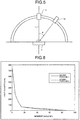
- a configuration of a device used in the experiment is shown in FIG. 5 .
- a power meter 12 was fixed at a position on a normal vector I with respect to a position of a target on a surface of a cast piece sample 14.
- Light receiving quantities of the power meter 12 when an incident angle ⁇ of a laser 13 relative to the normal vector I is changed from 0° to 90° were measured.
- the results of the experiment are shown in FIG. 6 .
- the light receiving quantities of the power meter 12 are large as a mirror reflection component is included, when the incident angle ⁇ becomes 60° or larger, the light receiving quantity of the power meter 12 significantly decreases. Therefore, as long as there is no problem in the detectivity, the smaller the incident angle of the illumination light L is, the larger the light receiving quantity is obtained.
- the resolution in a depth direction of an inspection target portion is dependent on an inclination angle of a defect and the resolution of the area sensors 4a, 4b.
- the inclination angle of a defect is an angle formed between a "normal vector of a defect portion" that is orthogonally projected on a "plane formed with a normal vector of a surface of a sound portion of the inspection target portion and a vector of a direction of a light source" and the normal vector of the surface of the sound portion.
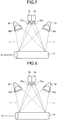
- the light source 2a, 2b are distinguished. Specifically, as shown in FIG. 7 , two kinds of wavelength selection filters 20a, 20b, wavelength regions of which do not overlap with the light sources 2a, 2b are arranged, and a wavelength region of the illumination light L is selected. Moreover, wavelength selection filters 21a, 21b having the same wavelength selection properties are arranged in the area sensors 4a, 4b.
- a reflection light of the illumination light L from the light source 2a is received only by the area sensor 4a by the wavelength selection filters 20a, 21a
- a reflection light of the illumination light L from the light source 2b is received only by the area sensor 4b by the wavelength selection filters 20b, 21b. Therefore, by matching the imaging timing of the area sensors 4a, 4b, two-dimensional images by reflection lights of the illumination lights L from the light sources 2a, 2b can be obtained without a positional deviation.
- the processing after imaging two-dimensional images is the same as that of the first mode.
- the light sources 2a, 2b can be used in a form of flash light sources, and the imaging time of two-dimensional images can be shortened without changing irradiation timing of the light sources 2a, 2b.
- a blue transmission filter is used as the wavelength selection filter 20a
- a green transmission filter is used as the wavelength selection filter 20b
- a two-dimensional image is imaged by using one unit of a color camera, and only a reflection light of the illumination light L from the light source 2a is received by a blue channel and only a reflection light of the illumination light L from the light source 2b is received in a green channel.
- the light sources 2a, 2b are distinguished.
- linear polarizing plates 30a, 30b are arranged at ⁇ ° and ( ⁇ +90)° ( ⁇ is an arbitrary angle) at the light sources 2a, 2b, and only light of polarization components orthogonal to each other is passed.
- the linear polarizing plate signifies a filter that passes only a linear polarization component in a certain direction of incident light.
- linear polarizing plates 31a, 31b having the same linear polarization properties as the linear polarizing plates 30a, 30b are arranged at ⁇ ° and ( ⁇ +90)° at the area sensors 4a, 4b.
- a reflection light of the illumination light L from the light source 2a is received only by the area sensor 4a, and a reflection light of the illumination light L from the light source 2b is received only by the area sensor 4b. Therefore, by matching the imaging timing of the area sensors 4a, 4b, two-dimensional images by reflection lights of the illumination lights L from the respective light sources can be obtained without a positional deviation.
- the light sources 2a, 2b can be used in a form of flash light sources, and the imaging time of two-dimensional images can be shortened without changing irradiation timing of the light sources 2a, 2b. Thereafter, the positioning and the processing after imaging two-dimensional images is the same as those of the first and the second modes.
- FIG. 9 depicts a result of the surface defect detection.
- FIG. 10(a) is a two-dimensional image that is acquired when the illumination light L is irradiated from the light source 2a
- FIG. 10 (b) is a two-dimensional image that is acquired when the illumination light L is irradiated from the light source 2b
- FIG. 10(a) is a two-dimensional image that is acquired when the illumination light L is irradiated from the light source 2a
- FIG. 10 (b) is a two-dimensional image that is acquired when the illumination light L is irradiated from the light source 2b
- FIG. 10(a) is a two-dimensional image that is acquired when the illumination light L is irradiated from the light source 2a
- FIG. 10 (b) is a two-dimensional image that is acquired when the illumination light L is irradiated from the light source 2b
- FIG. 10(a) is a two-dimensional image that is acquired when the illumination light L is irradiated from
- 10(c) is a difference image between the two-dimensional image shown in FIG. 10 (a) and the two-dimensional image shown in FIG. 10 (b) .
- SN ratios of the images shown in FIG. 10 (a) to (c) are, sequentially 3.5, 3.5, and 6.0, and the SN ratio of the difference image was improved compared to when the illumination light L is irradiated simply from one direction.
- FIG. 11 is a diagram showing a result of the surface defect detection processing performed on a steel pipe portion at which a scale has appeared.
- FIG. 11 (a) is a two-dimensional image that is acquired when the illumination light L is irradiated from the light source 2a
- FIG. 11 (b) is a two-dimensional image that is acquired when the illumination light L is emitted from the light source 2b
- FIG. 11 (c) is a difference image between the two-dimensional image shown in FIG. 11 (a) and the two-dimensional image shown in FIG. 11 (b) .
- Black spots spread throughout the two-dimensional images shown in FIG. 11 (a) and (b) are a scale to be a noise.
- the shape of the scale is flat, by acquiring the difference image, the image of the scale was removed.
- a signal of the scale to be a noise was suppressed to about 1/4, compared to a case when the illumination light L is irradiated simply from one direction.
- FIG. 12 is a schematic diagram showing a configuration of a modification of the surface defect detection device of the first embodiment of the present invention.
- an illumination light irradiated from a single unit of the light source 2a is divided by mirrors 40a, 40b, 40c, 40d, and is irradiated to an inspection target portion of the steel pipe P1 finally from two directions.
- the wavelength selection filters 20a, 20b, or the linear polarizing plates 30a, 30b in respective optical paths, an effect similar to the second and the third modes can be obtained.
- the present modification is to irradiate the illumination light from two directions, the same applies also when the illumination light is irradiated from three or more directions.
- FIG. 13 is a schematic diagram showing a configuration of another modification of the surface defect detection device of the first embodiment of the present invention.
- a wavelength of a light source is limited not by the wavelength selection filters 20a, 20b, but a wavelength of a light source is limited by using pulse lasers 51a, 51b, and diffusers 50a, 50b.
- laser beams from the pulse lasers 51a, 51b having different wavelength regions from each other are irradiated from right and left directions of the inspection target portion, thereby distinguishing light sources.
- the diffusers 50a, 50b are inserted in the optical paths of the laser beams.
- the illumination light is irradiated from two directions, the same applies to a case in which the illumination light is irradiated from three or more directions.
- a dichroic mirror is used in the surface defect detection device shown in FIG. 7 .
- the dichroic mirror is a mirror that reflects light of a specific wavelength component, and passes light of other wavelength components. By using the dichroic mirror, the wavelength selection filters become unnecessary.
- the illumination light is irradiated from two directions, the same applies to a case in which the illumination light is irradiated from three or more directions.
- FIG. 14 a configuration and an operation of a surface defect detection device according to a second embodiment of the present invention are explained referring to FIG. 14 , and FIG. 22 .
- the configuration of the surface defect detection device of the present embodiment is the same as the configuration of the surface defect detection device of the first embodiment described above, explanation of the configuration is omitted below, and only the operation of the surface defect detection device is explained.
- the surface defect detection device 1 of the second embodiment of the present embodiment distinguishes a scale or a harmless pattern at an inspection target portion from a concavo-convex surface defect by performing surface defection detection processing described below.
- the scale or the harmless pattern signifies a surface coat or a portion that has a surface condition with different optical characteristics from a base steel portion having thickness of several ⁇ m to several tens of ⁇ m, and is a portion to be a cause of a noise in the surface defect detection processing.
- the image processing device 5 performs image processing such as calibration, shading correction, and noise removal, using camera parameters that have been derived in advance for two two-dimensional images input from the area sensors 4a, 4b, and then performs difference processing between the two-dimensional images to generate a difference image, and detects a concavo-convex surface defect at the inspection target portion is detected from the generated difference image.
- image processing such as calibration, shading correction, and noise removal
- a luminance value of each pixel constituting the two-dimensional image Ia that is been acquired when the illumination light L is irradiated from the light source 2a is denoted as Ia(x, y) (where the number of pixels is XxY, an x-coordinate is 1 ⁇ x ⁇ X, and a y-coordinate is 1 ⁇ y ⁇ Y)
- a luminance value of each pixel constituting the two-dimensional image Ib that is acquired when the illumination light L is irradiated from the light source 2b is denoted as Ib(x, y)
- the luminance value I_diff(x, y) of each pixel of the difference image I_diff acquired by the difference processing is expressed by Equation (1) that has already been described.
- FIG. 14 (a), (b) depict shades when illumination light is irradiated to an inspection target portion from one of the light sources when surface of the inspection target portion shapes are a concave shape and a convex shape, respectively.
- FIG. 14 (a) when the surface shape is a concave shape, a portion closer to the light source is dark as a light quantity of the illumination light per unit area decreases, and a portion on the opposite side to the light source is bright as it is closer to the regular reflection direction.
- FIG. 14 (a) depict shades when illumination light is irradiated to an inspection target portion from one of the light sources when surface of the inspection target portion shapes are a concave shape and a convex shape, respectively.
- brightness patterns of reflection lights of the illumination light vary depending on a surface shape of an inspection target portion being a concave shape or a convex shape. Therefore, by recognizing brightness patterns of reflection lights, presence or absence of a concavo-convex surface defect can be detected.
- a method of detecting a concavo-convex surface defect by recognition of brightness patterns of reflection lights is described. In the following, out of concavo-convex surface defects, a surface defect of a concave shape is to be detected, but a surface defect of a convex shape can also be detected by the same logic.
- a bright portion described below signifies a blob that has an area equal to or larger than a predetermined value obtained by performing linkage processing of pixels having brightness equal to or higher than a predetermined threshold in the difference image I_diff.
- a dark portion described below signifies a blob that has an area equal to or larger than a predetermined value obtained by performing the linkage processing of pixels having brightness equal to or lower than a predetermined threshold in the difference image I_diff.
- Blob signifies a set of labeled pixels.
- a bright portion and a dark portion are extracted by performing threshold processing, and a brightness pattern is thereby recognized.
- the surface defect detection device 1 of the present embodiment as the light sources 2a, 2b are arranged symmetrically about a normal vector of an inspection target portion, brightness patterns of reflection lights caused by a convex and concave shape on a surface are generated in left and right directions. Because bright/dark are positioned opposite on right and left depending on order of the difference processing, in this example, when a right side is bright and a left side is dark, it is a concave shape, and when a right side is dark and a left side is bright, it is a convex shape.
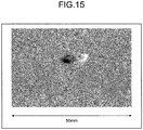
- the difference image I_diff of a surface defect in a concave shape is as shown in FIG. 15 .
- the and -The, binarized images I_blight, I_dark of the bright portion and the dark portion are expressed as in Equation (4) below.
- I _ blight x , y 1 w h e n I _ diff x , y ⁇
- the I _ blight x , y 0 w h e n I _ diff x , y ⁇
- the I _ dark x , y 1 w h e n I _ diff x , y ⁇ ⁇
- the I _ dark x , y 0 w h e n I _ diff x , y > ⁇
- the _ dark x , y 0 w h e n I _ diff x , y > ⁇
- a positional relationship of the bright portion and the dark portion are calculated, thereby detecting presence or absence of a concavo-convex surface defect.
- a calculation method of a positional relationship of a bright portion and a dark portion there are various methods as a calculation method of a positional relationship of a bright portion and a dark portion, and representative three calculation methods are described below, but another calculation method can also be applied as long as a positional relationship of a bright portion and a dark portion can be calculated.
- a first positional-relationship calculation method is a method of calculating a positional relationship of a bright portion and a dark portion by subjecting a bright portion and a dark portion to expansion and contraction processing in a specific direction.
- a flowchart of this calculation method is shown in FIG. 16 .
- a case of recognizing a brightness pattern in which a right side is bright and a left side is dark to detect a surface defect in a concave shape is explained. That a right side is bright and a left side is dark means that a dark portion is always present on a left side of a bright portion, and that a bright portion is always present on a right side of a dark portion.
- the image processing device 5 performs expansion processing in a left direction for a bright portion (steps S1a, S1b).
- images of the bright portion and the dark portion subjected to the expansion processing are I_blight_extend, I_dark_extend, and a length to be expanded is W
- the expansion processing is expressed as in Equation (5) below where an upper left point of a two-dimensional image is an origin point, a downward direction is a y-axis positive direction, and a rightward direction is an x-axis positive direction.
- the bright portion and the dark portion are expanded by the same length W, but the length W to be expanded is not required to be the same, and in an extreme case, only one of the bright portion and the dark portion can be subjected to the expansion processing. Moreover, the length W to be expanded depends also on the size of a surface defect wished to be detected.
- the image processing device 5 performs and processing on the images of the bright portion and the dark portion I_blight_extend, I_dark_extend subjected to the expansion processing, and thereby extracts an overlapped portion of the images of the bright portion and the dark portion I_blight_extend, I_dark_extend subjected to the expansion processing, as a defect candidate image I_defect (steps S2a, S2b) .
- I _ defect I _ blight _ extend & I _ dark _ extend
- the image processing device 5 performs linkage and isolated-point removal processing for each of the acquired defect candidate images I_defect as necessary, and then performs labeling processing, thereby generating a defect candidate blob I_defect_blob (step S3).
- the image processing device 5 then extracts a feature quantities of each of the defect candidate blobs I_defect_blob, and determined whether each of the defect candidate blobs I_defect_blob is a surface defect of a concave shape based on a result of extraction (steps S4a, S4b). As information about the bright portion and the dark portion is necessary to find a feature quantities of the defect candidate blob I_defect_blob, the bright portion and the dark portion are reconstructed from the detect candidate blob I_defect_blob.
- the image processing device 5 searches the dark portion binarized image I_dark toward the left side from a centroid of the defect candidate blob I_defect_blob as a starting point, and regards a blob found first as a dark portion defect candidate blob I_dark_blob.
- the image processing device 5 searches the bright portion binarized image I_blight toward the right side from the centroid of the defect candidate blob I_defect_blob as a starting point, and regards a blob first found as a bright portion defect candidate blob I_blight_blob.
- the image processing device 5 extracts a feature quantities from the bright portion defect candidate blob I_blight_blob and the dark portion defect candidate blob I_dark_blob thus reconstructed, and determines whether each of the defect candidate blobs I_defect_blob is a surface defect of a concave shape based on the extracted feature quantities.
- a specific feature quantities varies depending on a defect, it is not specifically described herein, but one example is given in an example.
- a bright portion and a dark portion are extracted to be subjected to labeling, and by recognizing a positional relationship of the bright portion and the dark portion, a surface defect of a concave shape is detected.
- the image processing device 5 recognizes a bright portion and a dark portion individually by labeling, and acquires information of a centroid of the bright portion and the dark portion.
- the image processing device 5 determines whether a centroid of the dark portion is present in a predetermined range on a right side of each of the bright portions based on the information of a centroid of the bright portion and the dark portion.
- the image processing device 5 recognizes a combination of the bright portion and the dark portion be a pair, as a brightness pattern, and determines whether it is a surface defect of a concave shape by performing feature quantity analysis of the brightness pattern.
- the brightness pattern is recognized using the information of a centroid herein, information used for recognition of a brightness pattern is not necessarily required to be information of a centroid as long as it is information with which positions of the bright portion and the dark portion can be grasped (for example, an upper end position, a lower end position, and the like)
- a brightness pattern is recognized by using a filter, and a surface defect is thereby detected.
- the surface defect detection device 1 shown in FIG. 1 as the light sources 2a, 2b are arranged symmetrically about a normal vector of an inspection target portion, a brightness pattern of a reflection light caused by a convex and concave shape on a surface is generated in left and right directions.
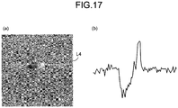
- FIG. 17 (a), (b) show one example of a difference image and a one-dimensional profile of a brightness pattern at a line segment L4 shown in FIG. 17 (a) , respectively.
- the one-dimensional profile of the brightness pattern is to be a one-dimensional profile having a characteristic that a peak is present on a right side and a valley is present on a left side. Therefore, in the present embodiment, a filter H in which a right has a peak and a left side has a valley is generated in advance, and as indicated in Equation (7) below, by applying the filter H to the difference image I_diff, high frequency noises are reduced, and a two-dimensional image I_cont in which only a brightness pattern is emphasized is generated.
- I _ cont H * I _ diff
- FIG. 18 (a), (b) show a two-dimensional image of the filter H that is generated in advance, and one example of a one-dimensional profile thereof on a left side and a right side, respectively.
- FIG. 19 (a), (b) show a difference image obtained by performing filter processing using the filter H shown in FIG. 18 (a), (b) , and one example of a one-dimensional profile thereof of a left side and a right side, respectively.
- FIG. 19 (a), (b) it is found that a two-dimensional image in which high frequency noises are reduced, and only the brightness pattern is emphasized is obtained.
- the image processing device 5 performs the linkage and isolated-point removal processing as necessary on the two-dimensional image in which the brightness pattern is thus emphasized, and then performs the threshold processing, thereby extracting the defect candidate image I_defect.
- the image processing device 5 detects a surface defect of a concave shape by subjecting the extracted defect candidate image I_defect to processing similar to that in the first positional-relationship calculation method.
- the surface defect detection processing of the second embodiment of the present invention irradiates the illumination lights L to the same inspection target portion from different directions at substantially identical incident angles using the two distinguishable light sources 2a, 2b, acquires images formed by reflection lights of the respective illumination lights L, extracts a bright portion and a dark portion of an image acquired by performing the difference processing between the acquired images, and determines whether a concavo-convex surface defect is present based on a positional relationship of the extracted bright portion and dark portion, and the irradiation directions of the illumination lights L, and therefore, can distinguish a scale or a harmless pattern from a concavo-convex surface defect accurately.
- the light sources are arranged bilaterally symmetrically on right and left sides, brightness patterns of right and left are recognized, even if the light sources are arranged not bilaterally, but vertically symmetrically, or not symmetrically, a concavo-convex surface defect can be detected by similar processing.
- the light sources are arranged vertically symmetrically, only the directions of the brightness patterns are changed from a lateral direction to a vertical direction. Therefore, by rotating the brightness patterns by 90°, a concavo-convex surface defect can be detected by similar processing.
- FIG. 20 when the light sources are arranged such that the irradiation directions of the illumination lights differ by 90°, with a surface defect of a concave shape, a portion closer to the light source is dark and a portion on the opposite side to the light source is bright, and with a surface defect of a convex shape, a portion closer to the light source is bright and a pat on the opposite side to the light source is dark.
- a surface defect has a concave shape
- a two-dimensional image acquired by the illumination light from the light source 2a is as shown in FIG. 21 (a)
- a two-dimensional image acquired by the illumination light from the light source 2b is as shown in FIG. 21 (b) .
- the difference image is to have a brightness pattern having a contrast from lower left to upper right as shown in FIG. 21 (c) . Accordingly, by rotating the brightness pattern by 45°, a concavo-convex surface defect can be detected by a method similar to a case of the brightness pattern in a bilateral direction. Moreover, by using three or more light sources, difference images of more than one pattern can be acquired, and detection accuracy of a surface defect can be further improved.
- a concavo-convex surface defect is detected when the illumination lights are irradiated from direction symmetric to a normal of an inspection target portion, the irradiation direction of the illumination lights are not necessarily required to be symmetrical.
- the surface defect detection processing of the present embodiment can be applied to general manufacturing lines of steel products regardless of hot working or cold working.
- the surface defect detection processing using the first positional-relation calculation method described above was applied to an inspection target portion in which a pit flaw was formed and a sound inspection target portion in which a pit flaw was not formed.
- a feature quantitity a brightness ratio, an area ratio, and a degree of circularity of a bright portion and a dark portion were calculated.
- the degree of circularity is a value normalized by dividing an area of a bright portion and a dark portion by a square of a length of a perimeter thereof, and is used to determine whether a shape of a bright portion and a dark portion is close to circle.
- an optimal range of an incident angle of an illumination light of each light source with respect to an inspection target portion is reviewed.
- the present invention features irradiation of illumination lights to an inspection target portion from two or more different directions, and in the following, for simplicity, an optimal range of an incident angle of an illumination light when illumination lights are irradiated from oblique directions symmetric to each other about a normal vector of an inspection target portion is reviewed. Furthermore, in the following, an intensity of an image signal of a surface defect when it is assumed that a surface condition of an inspection target portion is uniform is reviewed.
- a left side of a screen and a right side of the screen when an illumination light is irradiated from a left side in a field of view of an area sensor 4 are expressed as “closer side” and “far side”, respectively, and a left side of the screen and the right side of the screen when an illumination light is irradiated from a right side of the field of view of the area sensor 4 are expressed as "far side” and "closer side”, respectively.
- a direction of a normal vector at a surface defect portion differs from a normal vector at a sound portion. Therefore, conditions of light emission and reception angles of illumination light in the surface defect portion differs from those of the sound portion, and a brightness pattern is generated.
- a concave defect D having a V shape is present on a steel product surface S, and the illumination lights L are irradiated thereto from left and right directions, and an image of the steel product surface S is captured from a front side by the area sensor 4 is considered.
- an irradiated light quantity of the illumination light L per unit area becomes small compared to a flat portion, and the intensity of an image signal decreases as it departs from a mirror reflection condition (regular reflection condition).
- a mirror reflection condition regular reflection condition
- the irradiation light quantity of the illumination light L per unit area becomes large compared to the flat portion, and the intensity of an image signal increases as it becomes closer to the mirror reflection condition.
- the mirror reflection condition described above is a condition that the light source and the area sensor are positioned symmetrically about a normal vector of a surface of a sound portion, that is a condition that an incident angle and a reflection angle of an illumination light are equal to each other.
- a positional relationship between a bright portion and a dark portion is also reversed for the light source on the right side and the light source on the left side. Therefore, when two images captured by the area sensors 4 are subjected to the difference processing, a brightness pattern can be acquired. That is, according to how inclined relative to the flat portion, the intensity of an image signal varies. A sound portion also has surface roughness, and is not completely flat. Therefore, when the incident angle of the illumination light is increased to significantly large, a signal caused by minute concavity and convexity on a surface becomes conspicuous, to be a cause of a noise.
- FIG. 24 is a diagram showing a configuration of a two-dimensional model of the optical system.
- an incident angle of the illumination light L from the light source 2 with respect to the steel product surface S normal vector I
- a reflection angle of the illumination light L entering the area sensor 4 is ⁇
- an inclination of an inspection target portion microscopically captured relative to an inclination of a reference surface of the steel product surface S as 0 is ⁇
- an incident light quantity of the illumination light L from the light source 2 to the inspection target portion is I 0
- a light quantity I of the illumination light L that enters the area sensor 4 is expressed by Equation (8) below.
- i I 0 R ⁇ , ⁇ , ⁇ , k
- R in Equation (8) indicates a function of a reflection intensity of the illumination light L, and is calculated by Equation (9) below.
- R ⁇ , ⁇ , ⁇ , k K 1 cos ⁇ ⁇ ⁇ + K 2 1 cos ⁇ ⁇ ⁇ e ⁇ ⁇ ⁇ ⁇ + ⁇ 2 2 2 ⁇ 2
- the first term on the right side of Equation (9) indicates an intensity of diffuse reflection of the illumination light L
- the second term indicates an intensity of the mirror reflection of the illumination light L
- a reflection intensity of the illumination light L is expressed by a sum of the first term and the second term.
- the illumination light L diffuses in all directions after entering the inspection target portion.
- the mirror reflection the illumination light L reflects in a direction symmetric to the normal vector of the inspection target portion the strongest, and the intensity of the illumination light L is attenuated as departing from the direction as Gaussian function.
- the inspection target portion itself is to be a shade, and the illumination light L is not irradiated, and therefore the reflection intensity of the illumination light L is 0.
- I 1 , I 2 indicate the incident light quantities of the illumination lights L to the target surface
- ⁇ 1 , ⁇ 2 indicate the incident angles of the illumination lights from the respective light sources to the target surface
- ⁇ indicates a reflection angle of the illumination light L that enters the area sensor 4
- ⁇ indicates an inclination of the target surface microscopically captured relative to an inclination of a reference surface as
- k is a parameter that expresses a surface condition of the target surface.
- the shading correction is then performed on the brightness i 1 , i 2 to remove unevenness in a light quantity of the light source 2 or unevenness in optical conditions.
- a method generally used in which a vector obtained by averaging a sum of brightness of respective pixels in a vertical direction (referred to as "vertical average vector") is generated, subtraction and division are performed on all rows of an image by the vertical average vector, and a signal is further subjected to constant multiplication to be normalized was used. Furthermore, on a resultant image, the same processing is performed also in a horizontal direction, thereby performing the shading correction.
- Equation (12) when signals when the target surface is a sound portion are expressed as i 10 , i 20 , and a surface condition of the sound portion is expressed as k 0 , it is expressed as in Equations (12), (13) below.
- i 10 I 1 R ⁇ 1 , ⁇ ,0, k 0
- i 20 I 2 R ⁇ 2 , ⁇ ,0, k 0
- Equation (14) expresses the brightness i 1 after the shading correction
- Equation (15) expresses the brightness i 2 after the shading correction
- Equation (16) expresses the brightness of the difference image.
- an optimal range of an incident angle of the illumination light was derived from the intensity of image signals of the sound portion and the surface defect portion by using the above model.
- a parameter expressing a surface condition of the steel product surface was experimentally acquired. Specifically, an image of a steel product that has a general surface condition was actually captured by an area sensor, and a brightness profile (image profile) of an actual image signal was adjusted to a brightness profile (theoretical curve) of a theoretical image signal that had been acquired by simulating an identical optical system. A result of adjustment is shown in FIG. 25 , and a configuration of the optical system used in the experiment is shown in FIG. 26 .
- a change of the S/N ratio of the image signal with respect to a change of an incident angle of the illumination light was simulated by using the acquired parameter k expressing the surface condition.
- illumination lights were irradiated from bilaterally symmetrical positions, and parameters expressing the surface conditions at the surface defect portion and the sound portion are identical.
- a contributing term is the inclination of the steel product surface. Therefore, before simulating a change of the S/N ratio of the image signal with respect to a change of the incident angle of the illumination light, surface shapes of the sound portion and the surface defect portion were measured, and the inclination relative to the reference surface was calculated.
- the inclination herein signifies an angle that is formed by two vectors at orthogonal projection when a normal vector of each surface and a normal vector of the steel product reference surface are orthogonally projected on a plane formed by the light source, the area sensor, and the inspection target portion.
- FIG. 27 and FIG. 28 show the inclinations of the surface defect portion and the sound portion, respectively.
- the surface of the surface defect portion has an inclination of 20° or larger for the smallest.
- a standard deviation of the inclination of the surface of the sound portion relative to the reference surface is about 3° to 5°.
- a signal of the surface defect portion is detected on a surface of the sound portion having some surface roughness. Therefore, regarding an image signal corresponding to an inclination of a surface of about 3° to 5° as a noise, a change of the S/N ratio with respect to a change of an incident angle of the illumination light was evaluated using an image signal corresponding to an inclination of a surface equal to or larger than 20°.
- the S/N ratio can be expressed as in Equations (17), (18) below.
- the optical system should be designed such that the incident angle ⁇ of the illumination light is within the range of 60° to 82.5° to detect a surface defect having a shallow angle with a low S/N ratio.
- the incident angle ⁇ of the illumination light is controlled to be 55° or smaller by the light quantity evaluation. This is because the light quantity of the reflection light significantly decreases if the incident angle ⁇ of the illumination light is increased.
- the incident angle ⁇ of the illumination light is preferable to be within the range of 60° to 82.5°.
- FIG. 31 A result of evaluation of the S/N ratio by performing the image processing described above actually changing the parameters of the light source is shown in FIG. 31 .
- the S/N ratio was highest when the incident angle ⁇ of the illumination light was in the range of 60° to 82.5°, and it was confirmed to match with the simulation result.
- the difference image acquired at this time is shown in FIG. 32 .
- the signal intensity of the difference image increased.
- the signal intensity of the difference image once decreased when the incident angle ⁇ of the illumination light is 70° the signal intensity of the difference image increased when the incident angle of the illumination light was further increased.
- the phenomenon that the signal intensity of the difference image once decreases when the incident angle ⁇ of the illumination light is 70° is considered be caused because the surface condition of the inspection target portion was different, and there was unevenness in a mirror property and a diffusion property even within the sound portion, not just due to the emission and reception angle of the illumination light.
- the light quantity of the reflection light significantly decreases when the incident angle ⁇ of the illumination light L is increased to be large, this condition is supposed to be used only in a state in which the light quantity of the reflection light is obtained. Therefore, by designing the optical system such that the incident angle ⁇ of the illumination light is within the range of 60° to 82.5°, a defect with a relatively shallow angle can also be detected with a high S/N ratio. Furthermore, although the present embodiment has been explained with a steel plate, similar consideration and application are possible for general steel products.
- FIG. 33 shows a configuration of the optical system that was used in this experiment.
- the incident angle ⁇ of the illumination light L toward a center of a field of view was 70°
- the resolution of the area sensor 4 was 1,0 mm/pixel
- the inspection range was 350 mm in width ⁇ 270 mm in length.
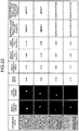
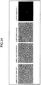
- FIG. 34 shows a result of the surface defect detection processing.
- FIG. 34(d) it was confirmed that the surface defect portion has a brightness pattern, and the surface defect was able to be detected.
- the surface defect portion shown in FIG. 34(d) is a portion in which a bright portion and a dark portion were overlapped with each other by expansion, and was obtained by acquiring an image signal corresponding to the inclination of 20° or larger.
- a surface defect detection method and a surface defect detection device that can distinguish a scale or a harmless pattern from a surface defect accurately can be provided. Moreover, according to the present invention, a method for manufacturing a steel product that enables to manufacture a steel product by accurately distinguishing a scale or a harmless pattern from a surface defect, and based on a distinction result can be provided.
Landscapes
- Physics & Mathematics (AREA)
- Health & Medical Sciences (AREA)
- Life Sciences & Earth Sciences (AREA)
- Chemical & Material Sciences (AREA)
- Analytical Chemistry (AREA)
- Biochemistry (AREA)
- General Health & Medical Sciences (AREA)
- General Physics & Mathematics (AREA)
- Immunology (AREA)
- Pathology (AREA)
- Engineering & Computer Science (AREA)
- Textile Engineering (AREA)
- Investigating Materials By The Use Of Optical Means Adapted For Particular Applications (AREA)
Abstract
Description
- The present invention relates to a surface defect detection method and a surface defect detection device that optically detect surface defects of a steel product, and to a method for manufacturing a steel product, the method detecting surface defects of the steel product using the surface defect detection method, and manufacturing the steel product on the basis of the detection results. Background
- In recent years, from the viewpoint of improving yield by preventing mass incompatibility, it is desired that, in manufacturing processes of steel products, surface defects of a steel product are detected in hot or cold conditions. The term "steel product" as used herein refers to an article of iron or steel, such a steel sheet or a shaped steel, including, for example, a seamless steel pipe, a welded steel pipe, a hot-rolled steel sheet, a cold-rolled steel sheet, and a thick plate, and to a semifinished product, such as a slab, produced in the process of manufacturing the article of iron or steel. For this reason, as a method for detecting the surface defects of the steel product, a method has been developed in which a billet in the manufacturing process of a seamless steel pipe is irradiated with light, light reflected therefrom is received, and a determination is made on the basis of the light quantity of the reflected light as to whether a surface defect is present (refer to Patent Literature 1). A method has also been developed in which visible light beams in a plurality of wavelength regions that neither affect nor are affected by self-emitting light emitted from a hot steel product and do not affect each other are emitted from mutually symmetrical directions oblique to a normal line to the surface of the hot steel product, an image formed by combined reflected light beams and images formed by the individual reflected light beams are obtained in the normal direction to the surface of the hot steel product, and a surface defect of the hot steel product is detected from a combination of these images (refer to Patent Literature 2).
-
- Patent Literature 1: Japanese Laid-open Patent Publication No.
11-37949 - Patent Literature 2: Japanese Laid-open Patent Publication No.
59-52735 - According to the method described in
Patent Literature 1, since harmless patterns and scale have different reflectance from that of a base steel portion, the sound harmless patterns or scale may be erroneously detected as the surface defects. For this reason, in the method described inPatent Literature 1, the billet is distinguished from the scale using the fact that the shape of the billet is linear. However, the surface defects of a steel product have not only linear shapes, but also various shapes, such as circular shapes. Therefore, the method described inPatent Literature 1 is difficult to be applied to the detection processing for the surface defects of the steel product. In the method described inPatent Literature 2, since a large number of types of surface defects, scale, harmless patterns and the like are present, simply combining the images is difficult to distinguish the surface defects from the scale or the harmless patterns. In addition, detection logic for dealing with a combination of a large number of images is realistically difficult to be established. - The present invention has been made in view of the above described problems, and an object thereof is to provide a surface defect detection method and a surface defect detection device that enable accurate distinction of the scale or the harmless patterns from the surface defects. Another object of the present invention is to provide a method for manufacturing a steel product, the method enabling the accurate distinction of the scale or the harmless patterns from the surface defects, and enabling manufacturing of the steel product on the basis of the distinction result.
- To solve the problem and achieve the object, a surface defect detection method of optically detecting a surface defect of a steel product according to the present invention includes: an irradiating step of irradiating illumination lights from different directions to an identical inspection target portion by using at least two distinguishable light sources; and a detecting step of acquiring images by reflection lights of the respective illumination lights and detecting a surface defect in the inspection target portion by performing difference processing between the acquired images, wherein an incident angle of the illumination lights of the respective light sources are within a range of 60° to 82.5° relative to the inspection target portion.
- Moreover, in the surface-defect detection method according to the present invention, the irradiating step includes a step of irradiating illumination lights by causing at least two flash light sources to emit light repeatedly such that light emission timing does not synchronize with each other, and/or a step of irradiating illumination lights of light sources, wavelength regions of which do not overlap with each other, and when the illumination lights of the light sources having the wavelength regions not overlapping one another are irradiated simultaneously, the detecting step includes a step of acquiring an image by a reflection light of each of the illumination lights by separating reflection lights of the respective mixed illumination lights by using filters that pass light having a wavelength identical to a wavelength of the illumination lights.
- Moreover, in the surface defect detection method according to the present invention, the detecting step includes a first determining step of extracting a bright portion and a dark portion of an image that has been acquired by performing difference processing on the acquired images, and of determining whether a concavo-convex surface defect is present based on a positional relationship between the extracted bright portion and dark portion, and an irradiation directions of the illumination lights.
- Moreover, a surface defect detection device that optically detects a surface defect of a steel product according to the present invention includes: an irradiating unit that irradiates illumination lights from different directions to an identical inspection target portion by using at least two distinguishable light sources; and a detecting unit that acquires images by reflection lights of the respective illumination lights and that detects a surface defect in the inspection target portion by performing difference processing between the acquired images, wherein an incident angle of the illumination lights of the respective light sources are within a range of 60° to 82.5° relative to the inspection target portion.
- Moreover, a method for manufacturing a steel product according to the present invention includes: a step of detecting a surface defect of a steel product by using the surface defect detection method according to the present invention; and of manufacturing a steel product based on a result of detection.
- A surface defect detection method and a surface defect detection device according to the present invention can accurately distinguish scale or harmless patterns from surface defects. A method for manufacturing a steel product according to the present invention enables the accurate distinction of the scale or the harmless patterns from the surface defects, and enables manufacturing of the steel product on the basis of the distinction result. Brief Description of Drawings
-
-
FIG. 1 is a schematic diagram showing a configuration of a surface defect detection device of a first embodiment of the present invention. -
FIG. 2 is a schematic diagram showing a configuration of a modification of an area sensor shown inFIG. 1 . -
FIG. 3 is a timing chart showing driving timing of a light source and the area sensor shown inFIG. 1 . -
FIG. 4 is a diagram showing one example of two two-dimensional images that have captured a surface defect, a scale, and a harmless pattern, and a difference image thereof. -
FIG. 5 is a schematic diagram showing a configuration of a device used for an experiment to study a relationship between an incident angle of illumination light and a reflectivity of a sound portion (base steel portion). -
FIG. 6 is a diagram showing a relationship between an incident angle of a laser and a light quantity received by a power meter. -
FIG. 7 is a schematic diagram for explaining surface defect detection processing of a second mode of the present invention. -
FIG. 8 is a schematic diagram for explaining surface defect detection processing of a third mode of the present invention. -
FIG. 9 is a schematic diagram showing a configuration of a device used in an example. -
FIG. 10 is a diagram showing a result of the surface defect detection processing of the example. -
FIG. 11 is a diagram showing a result of the surface defect detection processing performed on a steel pipe portion at which a scale has appeared. -
FIG. 12 is a schematic diagram showing a configuration of a modification of the surface defect detection device of the first embodiment of the present invention. -
FIG. 13 is a schematic diagram showing a configuration of another modification of the surface defect detection device of the first embodiment of the present invention. -
FIG. 14 is a diagram showing shadows created when light is irradiated from one direction when a surface shape of a target portion of inspection has a concave shape or a convex shape. -
FIG. 15 is a diagram showing one example of a difference image of a surface defect having a concave shape. -
FIG. 16 is a flowchart showing a flow of a method of calculating a positional-relationship of a bright portion and a dark portion using expansion processing. -
FIG. 17 is a diagram showing one example of a difference image and a primary profile of a brightness pattern. -
FIG. 18 is a diagram showing one example of a two-dimensional image of a filter and a primary profile. -
FIG. 19 is a diagram showing one example of a difference image subjected to filter processing using a filter shown inFIG. 18 and a primary profile. -
FIG. 20 is a schematic diagram showing a modification of an arrangement position of the light source. -
FIG. 21 is a schematic diagram showing a brightness pattern that is acquired with the arrangement position of the light source shown inFIG. 20 . -
FIG. 22 is a diagram showing a result of the surface defect detection processing of the example. -
FIG. 23 is a diagram for explaining a change of an image signal with a change of a positional relationship a surface of a concave-shaped defect relative to the light source. -
FIG. 24 is a diagram showing a configuration of a two-dimensional model of an optical system. -
FIG. 25 is a diagram showing a result of calibration of an image profile with respect to an ideal curve. -
FIG. 26 is a diagram showing a configuration of the optical system. -
FIG. 27 is a diagram showing an inclination of a surface of a surface defect portion. -
FIG. 28 is a diagram showing an inclination of a surface of a sound portion. -
FIG. 29 is a diagram showing a change of an SN ratio with respect to a change of an incident angle of the illumination light when the inclination of a surface of a sound portion is 3°. -
FIG. 30 is a diagram showing a change of the SN ratio with respect to a change of an incident angle of the illumination light when the inclination of a surface of a sound portion is 5°. -
FIG. 31 is a diagram showing changes of an image signal intensity and the SN ratio with respect to a change of an incident angle of the illumination light. -
FIG. 32 is a diagram showing one example of a difference image. -
FIG. 33 is a diagram showing a configuration of the optical system. -
FIG. 34 is a diagram showing a result of the surface defect detection processing performed on a steel plate. Description of Embodiments - A configuration and an operation of a surface defect detection device of the first to the third embodiments of the present invention are explained below referring to the drawings.
- First, a configuration and an operation of a surface defect detection device of a first embodiment of the present invention are explained, referring to
FIG. 1 to FIG. 13 . -
FIG. 1 is a schematic diagram showing a configuration of a surface defect detection device of a first embodiment of the present invention. As shown inFIG. 1 , a surfacedefect detection device 1 of the first embodiment of the present invention is a device that detects a surface defect of a steel pipe P in a cylindrical shape that is conveyed in a direction of an arrow in the figure, and that includeslight sources function generator 3,area sensors image processing device 5, and amonitor 6 as main components. - The
light sources function generator 3. It is desirable that thelight sources light sources - The
area sensors light sources function generator 3. Thearea sensors image processing device 5. It is desirable that thearea sensors - To solve the problem of positioning, it is desirable that the
area sensors FIG. 2 , either one of ahalf mirror 10, a beam splitter, and a prism can be used to adjust the optical axes of thearea sensors - The
image processing device 5 is a device that detects a surface defect at an inspection target portion by performing the difference processing described later on two two-dimensional images input from thearea sensors image processing device 5 outputs information about the two-dimensional images input from thearea sensors monitor 6. - The surface
defect detection device 1 having such a configuration distinguishes a scale or a harmless pattern at an inspection target portion from a surface defect by performing surface defect detection processing below. The surface defect described herein refers to a concavo-convex defect. Moreover, the scale or the harmless pattern signifies a surface coat or a portion that has a surface condition with different optical characteristics from a base steel portion having thickness of several µm to several tens of µm, and is a portion to be a cause of a noise in the surface defect detection processing. The following describes surface defect detection processing serving as first to third modes of the present invention. - First, the surface defect detection processing of the first mode of the present invention is explained referring to
FIG. 3 to FIG. 6 . -
FIG. 3 is a timing chart showing driving timing of thelight sources area sensors light sources area sensors 4a, 4b. in the surface defect detection processing of the first mode of the present invention, thelight sources light sources - That is, as shown in
FIG. 3 , in the present mode, thefunction generator 3 first transmits a trigger signal to thelight source 2a and thearea sensor 4a, and thelight source 2a irradiates the illumination light L, and thearea sensor 4a completes imaging of a two-dimensional image within time d. After completion of imaging of the two-dimensional image by thearea sensor 4a, thefunction generator 3 transmits a trigger signal to thelight source 2b and thearea sensor 4b, and a two-dimensional image is imaged similarly. According to the present mode, without causing light quantity reduction in a time difference d, two-dimensional images by individual reflection lights of the illumination lights L irradiated from the respective light sources can be imaged. - When a conveyance speed of the steel pipe P is high, it is preferable that the flash light sources have short light emitting time d. This is because as the light emitting time d becomes shorter, a shutter delay between two two-dimensional images acquired by the
area sensors 
- When the size of a surface defect of a detection target is, for example, 20 mm, empirically, a signal of at least five square pixels is necessary to detect a surface defect, and therefore, the resolution of 4mm/pixel is necessary. Furthermore, in this case, the allowable positional deviation due to irradiation timing of the illumination lights L is, empirically, necessary to be within 0.2 pixel, and therefore, when the conveyance speed of the steel pipe P is 1, 3, 5 m/sec, the light emitting time of the
light sources - In the present mode, the
image processing device 5 performs image processing, such as calibration, shading correction, and noise removal, using camera parameters that have been derived in advance for the two-dimensional images input from thearea sensors - Specifically, when a luminance value of each pixel constituting a two-dimensional image Ia that is been acquired when the illumination light L is irradiated from the
light source 2a is denoted as Ia(x, y) (where the number of pixels is XxY, an x-coordinate is 1≤x≤X, and a y-coordinate is 1≤y≤Y), a luminance value of each pixel constituting a two-dimensional image Ib that is acquired when the illumination light L is irradiated from thelight source 2b is denoted as Ib(x, y), a luminance value I_diff(x, y) of each pixel of a difference image I_diff thereof is expressed by Equation (2) below.
[Eq. 2]
- Examples of the two-dimensional images Ia, Ib that have captured a surface defect, and a scale and a harmless pattern, which are not defects, and the difference image I_diff thereof are given in
FIG. 4(a), (b), (c) , respectively. As shown inFIG. 4(a), (b), (c) , in a sound portion, regardless of a scale or a harmless pattern, an angle between a normal vector and thelight source 2a and an angle between a normal vector and thelight source 2b are equal to each other. Therefore, luminance value Ia (x, y)=luminance value Ib(x, y), that is, luminance value I_diff(x, y)=0 is obtained. However, in the surface defect portion, as the surface has a concave and convex shape, a portion in which the angle between the normal vector and thelight source 2a and the angle between the normal vector and thelight source 2b are not equal to each other is undoubtedly present. Therefore, luminance value Ia(x, y)≠luminance value Ib(x, y), that is, luminance value I_diff(x, y)≠0 is obtained. - Therefore, by generating a difference image of two two-dimensional images by a
difference unit 11, a scale or a harmless pattern that is not a defect is removed, and only a surface defect can be detected. By thus detecting a surface defect only, final evaluation of a surface defect whether to be harmful is performed based on various feature values, and a result of the evaluation is displayed on themonitor 6. - When there is a positional deviation between two two-dimensional images that influences a difference image, it is desirable that the influence of the positional deviation between the two-dimensional images be reduced by filtering with a two-dimensional low-pass filter. In this case, when the two-dimensional low-pass filter is denoted as H, a luminance value I'_diff(x, y) of the difference image is expressed by Equation (3) below.

- Moreover, it is preferable that the
light sources - Furthermore, it is desirable that an incident angle of the illumination light L be within such a range that a reflection light of a sound portion does not include a mirror reflection component, and a sufficient light quantity is obtained. The inventors of the present invention had an experiment to research a relationship between an incident angle of the illumination light L and a refractivity of a sound portion (base steel portion). A configuration of a device used in the experiment is shown in
FIG. 5 . As shown inFIG. 5 , in this experiment, apower meter 12 was fixed at a position on a normal vector I with respect to a position of a target on a surface of acast piece sample 14. Light receiving quantities of thepower meter 12 when an incident angle θ of alaser 13 relative to the normal vector I is changed from 0° to 90° were measured. The results of the experiment are shown inFIG. 6 . As shown inFIG. 6 , while in a range from 0° to 90° of the incident angle θ, the light receiving quantities of thepower meter 12 are large as a mirror reflection component is included, when the incident angle θ becomes 60° or larger, the light receiving quantity of thepower meter 12 significantly decreases. Therefore, as long as there is no problem in the detectivity, the smaller the incident angle of the illumination light L is, the larger the light receiving quantity is obtained. - The resolution in a depth direction of an inspection target portion is dependent on an inclination angle of a defect and the resolution of the
area sensors incident angle 45°, a defect signal can be detected by the difference processing. Therefore, assuming that the resolution of one pixel is 0.5 mm, the resolution in a depth direction of about 0.5×tan10°=0.09 mm is to be obtained theoretically. - Next, surface defect detection processing of a second mode of the present invention is explained referring to
FIG. 7 . - In the surface defect detection processing of the second mode of the present invention, by using light sources having wavelength regions not overlapping one another as the
light source light source FIG. 7 , two kinds ofwavelength selection filters light sources wavelength selection filters area sensors - With such a configuration, a reflection light of the illumination light L from the
light source 2a is received only by thearea sensor 4a by thewavelength selection filters light source 2b is received only by thearea sensor 4b by thewavelength selection filters area sensors light sources - When a moving speed of an inspection target portion is high, to prevent a positional deviation due to movement of the inspection target portion, the
light sources light sources wavelength selection filter 20a, a green transmission filter is used as thewavelength selection filter 20b, and a two-dimensional image is imaged by using one unit of a color camera, and only a reflection light of the illumination light L from thelight source 2a is received by a blue channel and only a reflection light of the illumination light L from thelight source 2b is received in a green channel. - Next, surface defect detection processing of a third mode of the present invention is explained referring to
FIG. 8 . - In the surface defection detection processing of the third mode of the present invention, by using light sources having linear polarization properties orthogonal to each other are used as the
light sources light sources FIG. 8 , linearpolarizing plates light sources polarizing plates polarizing plates area sensors - With such a configuration, a reflection light of the illumination light L from the
light source 2a is received only by thearea sensor 4a, and a reflection light of the illumination light L from thelight source 2b is received only by thearea sensor 4b. Therefore, by matching the imaging timing of thearea sensors - When a moving speed of an inspection target portion is high, the
light sources light sources - In the present example, as shown in
FIG. 9 , flash light sources were used as thelight sources light sources area sensors FIG. 10 depicts a result of the surface defect detection.FIG. 10(a) is a two-dimensional image that is acquired when the illumination light L is irradiated from thelight source 2a,FIG. 10 (b) is a two-dimensional image that is acquired when the illumination light L is irradiated from thelight source 2b, andFIG. 10(c) is a difference image between the two-dimensional image shown inFIG. 10 (a) and the two-dimensional image shown inFIG. 10 (b) . SN ratios of the images shown inFIG. 10 (a) to (c) are, sequentially 3.5, 3.5, and 6.0, and the SN ratio of the difference image was improved compared to when the illumination light L is irradiated simply from one direction. -
FIG. 11 is a diagram showing a result of the surface defect detection processing performed on a steel pipe portion at which a scale has appeared.FIG. 11 (a) is a two-dimensional image that is acquired when the illumination light L is irradiated from thelight source 2a,FIG. 11 (b) is a two-dimensional image that is acquired when the illumination light L is emitted from thelight source 2b, andFIG. 11 (c) is a difference image between the two-dimensional image shown inFIG. 11 (a) and the two-dimensional image shown inFIG. 11 (b) . Black spots spread throughout the two-dimensional images shown inFIG. 11 (a) and (b) are a scale to be a noise. As the shape of the scale is flat, by acquiring the difference image, the image of the scale was removed. In addition, in the difference image, a signal of the scale to be a noise was suppressed to about 1/4, compared to a case when the illumination light L is irradiated simply from one direction. -
FIG. 12 is a schematic diagram showing a configuration of a modification of the surface defect detection device of the first embodiment of the present invention. As shown inFIG. 12 , in the present modification, an illumination light irradiated from a single unit of thelight source 2a is divided bymirrors wavelength selection filters polarizing plates -
FIG. 13 is a schematic diagram showing a configuration of another modification of the surface defect detection device of the first embodiment of the present invention. As shown inFIG. 13 , in the present modification, in the surface defect detection device shown inFIG. 7 , a wavelength of a light source is limited not by thewavelength selection filters pulse lasers diffusers pulse lasers pulse lasers diffusers - In the present modification, in the surface defect detection device shown in
FIG. 7 , instead of thewavelength selection filters area sensors - Next, a configuration and an operation of a surface defect detection device according to a second embodiment of the present invention are explained referring to
FIG. 14 , andFIG. 22 . As the configuration of the surface defect detection device of the present embodiment is the same as the configuration of the surface defect detection device of the first embodiment described above, explanation of the configuration is omitted below, and only the operation of the surface defect detection device is explained. - The surface
defect detection device 1 of the second embodiment of the present embodiment distinguishes a scale or a harmless pattern at an inspection target portion from a concavo-convex surface defect by performing surface defection detection processing described below. The scale or the harmless pattern signifies a surface coat or a portion that has a surface condition with different optical characteristics from a base steel portion having thickness of several µm to several tens of µm, and is a portion to be a cause of a noise in the surface defect detection processing. - In the surface defect detection processing of the second embodiment of the present invention, the
image processing device 5 performs image processing such as calibration, shading correction, and noise removal, using camera parameters that have been derived in advance for two two-dimensional images input from thearea sensors - Specifically, when a luminance value of each pixel constituting the two-dimensional image Ia that is been acquired when the illumination light L is irradiated from the
light source 2a is denoted as Ia(x, y) (where the number of pixels is XxY, an x-coordinate is 1≤x≤X, and a y-coordinate is 1≤y≤Y), a luminance value of each pixel constituting the two-dimensional image Ib that is acquired when the illumination light L is irradiated from thelight source 2b is denoted as Ib(x, y), the luminance value I_diff(x, y) of each pixel of the difference image I_diff acquired by the difference processing is expressed by Equation (1) that has already been described. - As shown in
FIG. 4 , in a sound portion, regardless of presence or absence of a scale or a harmless pattern, an angle between a normal vector of a surface and thelight source 2a and an angle between a normal vector of a surface and thelight source 2b are equal to each other. Therefore, luminance value Ia(x, y)=luminance value Ib(x, y), that is, luminance value I_diff(x, y)=0 is obtained. However, in the concavo-convex surface defect portion, as the surface has a concave and convex shape, a portion in which the angle between the normal vector of the surface and thelight source 2a and the angle between the normal vector of the surface and thelight source 2b are not equal to each other is undoubtedly present. Therefore, luminance value Ia(x, y)≠luminance value Ib(x, y), that is, luminance value I_diff(x, y)≠0 is obtained. Thus, by generating a difference image I_diff of two two-dimensional images by adifference unit 11, an image of a sound portion with a scale or a harmless pattern, which is not a defect, can be removed. - Next, a logic of detecting a concavo-convex surface defect from the difference image I_diff is explained.
FIG. 14 (a), (b) depict shades when illumination light is irradiated to an inspection target portion from one of the light sources when surface of the inspection target portion shapes are a concave shape and a convex shape, respectively. As shown inFIG. 14 (a) , when the surface shape is a concave shape, a portion closer to the light source is dark as a light quantity of the illumination light per unit area decreases, and a portion on the opposite side to the light source is bright as it is closer to the regular reflection direction. On the other hand, as shown inFIG. 14 (b) , when the surface shape of the inspection target portion is a convex shape, a portion closer to the light source is bright as it is closer to the regular reflection direction, and a portion on the opposite side to the light source is dark as it is in a shade of the convex shape. - That is, brightness patterns of reflection lights of the illumination light vary depending on a surface shape of an inspection target portion being a concave shape or a convex shape. Therefore, by recognizing brightness patterns of reflection lights, presence or absence of a concavo-convex surface defect can be detected. In the following, a method of detecting a concavo-convex surface defect by recognition of brightness patterns of reflection lights is described. In the following, out of concavo-convex surface defects, a surface defect of a concave shape is to be detected, but a surface defect of a convex shape can also be detected by the same logic. Moreover, a bright portion described below signifies a blob that has an area equal to or larger than a predetermined value obtained by performing linkage processing of pixels having brightness equal to or higher than a predetermined threshold in the difference image I_diff. Furthermore, a dark portion described below signifies a blob that has an area equal to or larger than a predetermined value obtained by performing the linkage processing of pixels having brightness equal to or lower than a predetermined threshold in the difference image I_diff. Blob signifies a set of labeled pixels.
- In the present embodiment, a bright portion and a dark portion are extracted by performing threshold processing, and a brightness pattern is thereby recognized. Specifically, in the surface
defect detection device 1 of the present embodiment, as thelight sources FIG. 15 . When each of images of a bright portion and a dark portion are binarized by brightness thresholds The and -The, binarized images I_blight, I_dark of the bright portion and the dark portion are expressed as in Equation (4) below.
- After thus binarizing the image of the bright portion and the dark portion, and performing linkage and isolated-point removal as necessary, a positional relationship of the bright portion and the dark portion are calculated, thereby detecting presence or absence of a concavo-convex surface defect. Note that there are various methods as a calculation method of a positional relationship of a bright portion and a dark portion, and representative three calculation methods are described below, but another calculation method can also be applied as long as a positional relationship of a bright portion and a dark portion can be calculated.
- A first positional-relationship calculation method is a method of calculating a positional relationship of a bright portion and a dark portion by subjecting a bright portion and a dark portion to expansion and contraction processing in a specific direction. A flowchart of this calculation method is shown in
FIG. 16 . In the present embodiment, a case of recognizing a brightness pattern in which a right side is bright and a left side is dark to detect a surface defect in a concave shape is explained. That a right side is bright and a left side is dark means that a dark portion is always present on a left side of a bright portion, and that a bright portion is always present on a right side of a dark portion. Therefore, in this calculation method, first, theimage processing device 5 performs expansion processing in a left direction for a bright portion (steps S1a, S1b). When images of the bright portion and the dark portion subjected to the expansion processing are I_blight_extend, I_dark_extend, and a length to be expanded is W, the expansion processing is expressed as in Equation (5) below where an upper left point of a two-dimensional image is an origin point, a downward direction is a y-axis positive direction, and a rightward direction is an x-axis positive direction.
- In the present embodiment, the bright portion and the dark portion are expanded by the same length W, but the length W to be expanded is not required to be the same, and in an extreme case, only one of the bright portion and the dark portion can be subjected to the expansion processing. Moreover, the length W to be expanded depends also on the size of a surface defect wished to be detected.
- Next, as expressed by Equation (6) below, the
image processing device 5 performs and processing on the images of the bright portion and the dark portion I_blight_extend, I_dark_extend subjected to the expansion processing, and thereby extracts an overlapped portion of the images of the bright portion and the dark portion I_blight_extend, I_dark_extend subjected to the expansion processing, as a defect candidate image I_defect (steps S2a, S2b) .
- Next, the
image processing device 5 performs linkage and isolated-point removal processing for each of the acquired defect candidate images I_defect as necessary, and then performs labeling processing, thereby generating a defect candidate blob I_defect_blob (step S3). Theimage processing device 5 then extracts a feature quantities of each of the defect candidate blobs I_defect_blob, and determined whether each of the defect candidate blobs I_defect_blob is a surface defect of a concave shape based on a result of extraction (steps S4a, S4b). As information about the bright portion and the dark portion is necessary to find a feature quantities of the defect candidate blob I_defect_blob, the bright portion and the dark portion are reconstructed from the detect candidate blob I_defect_blob. - Specifically, because a bright portion is always present on a right side, and a dark portion is always present on a left side of a defect candidate portion, the
image processing device 5 searches the dark portion binarized image I_dark toward the left side from a centroid of the defect candidate blob I_defect_blob as a starting point, and regards a blob found first as a dark portion defect candidate blob I_dark_blob. Similarly, theimage processing device 5 searches the bright portion binarized image I_blight toward the right side from the centroid of the defect candidate blob I_defect_blob as a starting point, and regards a blob first found as a bright portion defect candidate blob I_blight_blob. Theimage processing device 5 extracts a feature quantities from the bright portion defect candidate blob I_blight_blob and the dark portion defect candidate blob I_dark_blob thus reconstructed, and determines whether each of the defect candidate blobs I_defect_blob is a surface defect of a concave shape based on the extracted feature quantities. As a specific feature quantities varies depending on a defect, it is not specifically described herein, but one example is given in an example. - In a second positional-relationship calculation method, after performing the threshold processing described above, and performing the linkage and isolated-point removal processing as necessary, a bright portion and a dark portion are extracted to be subjected to labeling, and by recognizing a positional relationship of the bright portion and the dark portion, a surface defect of a concave shape is detected. Specifically, first, the
image processing device 5 recognizes a bright portion and a dark portion individually by labeling, and acquires information of a centroid of the bright portion and the dark portion. Next, theimage processing device 5 determines whether a centroid of the dark portion is present in a predetermined range on a right side of each of the bright portions based on the information of a centroid of the bright portion and the dark portion. When the centroid of the dark portion is present therein, theimage processing device 5 recognizes a combination of the bright portion and the dark portion be a pair, as a brightness pattern, and determines whether it is a surface defect of a concave shape by performing feature quantity analysis of the brightness pattern. Although the brightness pattern is recognized using the information of a centroid herein, information used for recognition of a brightness pattern is not necessarily required to be information of a centroid as long as it is information with which positions of the bright portion and the dark portion can be grasped (for example, an upper end position, a lower end position, and the like) - In a third positional-relationship calculation method, without performing the threshold processing described above, a brightness pattern is recognized by using a filter, and a surface defect is thereby detected. Specifically, in the surface
defect detection device 1 shown inFIG. 1 , as thelight sources FIG. 17 (a), (b) show one example of a difference image and a one-dimensional profile of a brightness pattern at a line segment L4 shown inFIG. 17 (a) , respectively. - As shown in
FIG. 17. (a), (b) , in a surface defect of a concave shape, as a right side is bright and a left side is dark, the one-dimensional profile of the brightness pattern is to be a one-dimensional profile having a characteristic that a peak is present on a right side and a valley is present on a left side. Therefore, in the present embodiment, a filter H in which a right has a peak and a left side has a valley is generated in advance, and as indicated in Equation (7) below, by applying the filter H to the difference image I_diff, high frequency noises are reduced, and a two-dimensional image I_cont in which only a brightness pattern is emphasized is generated.
-
FIG. 18 (a), (b) show a two-dimensional image of the filter H that is generated in advance, and one example of a one-dimensional profile thereof on a left side and a right side, respectively.FIG. 19 (a), (b) show a difference image obtained by performing filter processing using the filter H shown inFIG. 18 (a), (b) , and one example of a one-dimensional profile thereof of a left side and a right side, respectively. As shown inFIG. 19 (a), (b) , it is found that a two-dimensional image in which high frequency noises are reduced, and only the brightness pattern is emphasized is obtained. - Note that it can be arranged to support many surface defect sizes by preparing several kinds of filters having different ranges in a width direction as necessary. The
image processing device 5 performs the linkage and isolated-point removal processing as necessary on the two-dimensional image in which the brightness pattern is thus emphasized, and then performs the threshold processing, thereby extracting the defect candidate image I_defect. Theimage processing device 5 then detects a surface defect of a concave shape by subjecting the extracted defect candidate image I_defect to processing similar to that in the first positional-relationship calculation method. - As is obvious from the above explanation, the surface defect detection processing of the second embodiment of the present invention irradiates the illumination lights L to the same inspection target portion from different directions at substantially identical incident angles using the two
distinguishable light sources - Although in the present embodiment, as the light sources are arranged bilaterally symmetrically on right and left sides, brightness patterns of right and left are recognized, even if the light sources are arranged not bilaterally, but vertically symmetrically, or not symmetrically, a concavo-convex surface defect can be detected by similar processing. Specifically, when the light sources are arranged vertically symmetrically, only the directions of the brightness patterns are changed from a lateral direction to a vertical direction. Therefore, by rotating the brightness patterns by 90°, a concavo-convex surface defect can be detected by similar processing.
- Furthermore, as shown in
FIG. 20 , when the light sources are arranged such that the irradiation directions of the illumination lights differ by 90°, with a surface defect of a concave shape, a portion closer to the light source is dark and a portion on the opposite side to the light source is bright, and with a surface defect of a convex shape, a portion closer to the light source is bright and a pat on the opposite side to the light source is dark. Specifically, when a surface defect has a concave shape, a two-dimensional image acquired by the illumination light from thelight source 2a is as shown inFIG. 21 (a) , and a two-dimensional image acquired by the illumination light from thelight source 2b is as shown inFIG. 21 (b) . Therefore, the difference image is to have a brightness pattern having a contrast from lower left to upper right as shown inFIG. 21 (c) . Accordingly, by rotating the brightness pattern by 45°, a concavo-convex surface defect can be detected by a method similar to a case of the brightness pattern in a bilateral direction. Moreover, by using three or more light sources, difference images of more than one pattern can be acquired, and detection accuracy of a surface defect can be further improved. - Moreover, although in the present embodiment, a concavo-convex surface defect is detected when the illumination lights are irradiated from direction symmetric to a normal of an inspection target portion, the irradiation direction of the illumination lights are not necessarily required to be symmetrical. Furthermore, the surface defect detection processing of the present embodiment can be applied to general manufacturing lines of steel products regardless of hot working or cold working.
- In the present example, the surface defect detection processing using the first positional-relation calculation method described above was applied to an inspection target portion in which a pit flaw was formed and a sound inspection target portion in which a pit flaw was not formed. In the present example, as a feature quantitity, a brightness ratio, an area ratio, and a degree of circularity of a bright portion and a dark portion were calculated. The degree of circularity is a value normalized by dividing an area of a bright portion and a dark portion by a square of a length of a perimeter thereof, and is used to determine whether a shape of a bright portion and a dark portion is close to circle. As it is unlikely that the brightness and the area in right and left signals are significantly inconsistent if a surface defect is due to the same cause, by evaluating a balance between right and left using the brightness ratio and the area ratio, detection accuracy of a surface defect is improved. Furthermore, as it is quite unlikely that a bright portion and a dark portion to evaluate a shade is in a circular shape, and a subject in a shape close to circle can be determined to have another cause, the degree of circularity was included in the feature quantities. Moreover, it was arranged to be able to detect only a surface defect having an area equal to or larger than a predetermined value by calculating areas of a bright portion and a dark portion. Detection results are shown in
FIG. 22 . As shown inFIG. 22 , according to the present example, a pit flaw and a sound portion in which a pit flaw is not formed can be distinguished from each other accurately. - Finally, an optimal range of an incident angle of an illumination light of each light source with respect to an inspection target portion is reviewed. The present invention features irradiation of illumination lights to an inspection target portion from two or more different directions, and in the following, for simplicity, an optimal range of an incident angle of an illumination light when illumination lights are irradiated from oblique directions symmetric to each other about a normal vector of an inspection target portion is reviewed. Furthermore, in the following, an intensity of an image signal of a surface defect when it is assumed that a surface condition of an inspection target portion is uniform is reviewed. Moreover, in the following, a left side of a screen and a right side of the screen when an illumination light is irradiated from a left side in a field of view of an
area sensor 4 are expressed as "closer side" and "far side", respectively, and a left side of the screen and the right side of the screen when an illumination light is irradiated from a right side of the field of view of thearea sensor 4 are expressed as "far side" and "closer side", respectively. - As a surface defect generally has a concave and convex shape, a direction of a normal vector at a surface defect portion differs from a normal vector at a sound portion. Therefore, conditions of light emission and reception angles of illumination light in the surface defect portion differs from those of the sound portion, and a brightness pattern is generated. Specifically, as shown in
FIG. 23 , a case in which a concave defect D having a V shape is present on a steel product surface S, and the illumination lights L are irradiated thereto from left and right directions, and an image of the steel product surface S is captured from a front side by thearea sensor 4 is considered. In this case, on a plane DA of the concave defect D on a closer side to the light source on a right side, an irradiated light quantity of the illumination light L per unit area becomes small compared to a flat portion, and the intensity of an image signal decreases as it departs from a mirror reflection condition (regular reflection condition). On the other hand, on a plane DB of the concave defect D on a far side from the light source on the right side, the irradiation light quantity of the illumination light L per unit area becomes large compared to the flat portion, and the intensity of an image signal increases as it becomes closer to the mirror reflection condition. The mirror reflection condition described above is a condition that the light source and the area sensor are positioned symmetrically about a normal vector of a surface of a sound portion, that is a condition that an incident angle and a reflection angle of an illumination light are equal to each other. - As the positional relationship between the light source and the surface of the concave defect D is reversed for the light source on the right side and the light source on the left side, a positional relationship between a bright portion and a dark portion is also reversed for the light source on the right side and the light source on the left side. Therefore, when two images captured by the
area sensors 4 are subjected to the difference processing, a brightness pattern can be acquired. That is, according to how inclined relative to the flat portion, the intensity of an image signal varies. A sound portion also has surface roughness, and is not completely flat. Therefore, when the incident angle of the illumination light is increased to significantly large, a signal caused by minute concavity and convexity on a surface becomes conspicuous, to be a cause of a noise. - Next, a physical phenomenon relating to a detection performance for a surface defect is explained. To study this physical phenomenon more precisely, an optical system is modeled in the following. In this example, a simplified Torrance-Sparrow model, which is one of a reflection model according to a physical phenomenon widely used in an optical simulation is used (cited literature (refer to "Illumination Distribution from Shadows", Ito, et al., Journal of Information Processing: Computer Vision and Image Media, vol. 41, No. ). Although the optical system is supposed to be handled by a three-dimensional model, for simplicity, a two-dimensional model is used in the following.
-
FIG. 24 is a diagram showing a configuration of a two-dimensional model of the optical system. As shown inFIG. 24 , when an incident angle of the illumination light L from thelight source 2 with respect to the steel product surface S (normal vector I) is α, a reflection angle of the illumination light L entering thearea sensor 4 is β, an inclination of an inspection target portion microscopically captured relative to an inclination of a reference surface of the steel product surface S as 0 is φ, an incident light quantity of the illumination light L from thelight source 2 to the inspection target portion is I0, and a parameter (vector volume) expressing a surface condition of the inspection target portion is k=(K1, K2, σ), a light quantity I of the illumination light L that enters thearea sensor 4 is expressed by Equation (8) below.
- Moreover, R in Equation (8) indicates a function of a reflection intensity of the illumination light L, and is calculated by Equation (9) below.

- The first term on the right side of Equation (9) indicates an intensity of diffuse reflection of the illumination light L, the second term indicates an intensity of the mirror reflection of the illumination light L, and a reflection intensity of the illumination light L is expressed by a sum of the first term and the second term. In the diffuse reflection, the illumination light L diffuses in all directions after entering the inspection target portion. On the other hand, in the mirror reflection, the illumination light L reflects in a direction symmetric to the normal vector of the inspection target portion the strongest, and the intensity of the illumination light L is attenuated as departing from the direction as Gaussian function. Moreover, k=(K1, K2, σ) is the term derived from a surface condition of the inspection target portion, and determines a spreading degree in the mirror reflection, and an intensity ratio of the mirror reflection and the diffuse reflection. However, when the incident angle α and the inclination φ satisfy a condition: π/2≤α+φ or α+φ≤-π/2, the inspection target portion itself is to be a shade, and the illumination light L is not irradiated, and therefore the reflection intensity of the illumination light L is 0.
- When brightness i1, i2 at certain points (hereinafter, described as target surface) on an image of the inspection target portion when the illumination light is irradiated from one light source (left side) and when the illumination light is irradiated from the other light source (right side) are calculated, expressing the intensity of an image signal received by the
area sensor 4 by using such a two-dimensional model, the brightness i1, i2 are expressed by Equations (10), (11).

- In Equations (10), (11), I1, I2 indicate the incident light quantities of the illumination lights L to the target surface, α1, α2 indicate the incident angles of the illumination lights from the respective light sources to the target surface, β indicates a reflection angle of the illumination light L that enters the
area sensor 4, φ indicates an inclination of the target surface microscopically captured relative to an inclination of a reference surface as 0, and k is a parameter that expresses a surface condition of the target surface. - When the brightness i1, i2 are calculated, the shading correction is then performed on the brightness i1, i2 to remove unevenness in a light quantity of the
light source 2 or unevenness in optical conditions. Although there are various methods for the shading correction, a method generally used in which a vector obtained by averaging a sum of brightness of respective pixels in a vertical direction (referred to as "vertical average vector") is generated, subtraction and division are performed on all rows of an image by the vertical average vector, and a signal is further subjected to constant multiplication to be normalized was used. Furthermore, on a resultant image, the same processing is performed also in a horizontal direction, thereby performing the shading correction. In detail, when signals when the target surface is a sound portion are expressed as i10, i20, and a surface condition of the sound portion is expressed as k0, it is expressed as in Equations (12), (13) below.

- Therefore, luminance values of an image after the shading correction and of the difference image are expressed as Equations (14) to (16) below. Equation (14) expresses the brightness i1 after the shading correction, Equation (15) expresses the brightness i2 after the shading correction, and Equation (16) expresses the brightness of the difference image.


- In this review, an optimal range of an incident angle of the illumination light was derived from the intensity of image signals of the sound portion and the surface defect portion by using the above model. At the derivation, first, a parameter expressing a surface condition of the steel product surface was experimentally acquired. Specifically, an image of a steel product that has a general surface condition was actually captured by an area sensor, and a brightness profile (image profile) of an actual image signal was adjusted to a brightness profile (theoretical curve) of a theoretical image signal that had been acquired by simulating an identical optical system. A result of adjustment is shown in
FIG. 25 , and a configuration of the optical system used in the experiment is shown inFIG. 26 . As a result, the parameter expressing the surface condition of the steel product surface was acquired as k=(K1, K2, σ)=(1000, 200, 0.21). Next, a change of the S/N ratio of the image signal with respect to a change of an incident angle of the illumination light was simulated by using the acquired parameter k expressing the surface condition. - For simplicity, an imaging direction of the area sensor is on a normal of the reference surface, that is, β=0, illumination lights were irradiated from bilaterally symmetrical positions, and parameters expressing the surface conditions at the surface defect portion and the sound portion are identical. In this surface defect detection processing, a contributing term is the inclination of the steel product surface. therefore, before simulating a change of the S/N ratio of the image signal with respect to a change of the incident angle of the illumination light, surface shapes of the sound portion and the surface defect portion were measured, and the inclination relative to the reference surface was calculated. The inclination herein signifies an angle that is formed by two vectors at orthogonal projection when a normal vector of each surface and a normal vector of the steel product reference surface are orthogonally projected on a plane formed by the light source, the area sensor, and the inspection target portion.
FIG. 27 andFIG. 28 show the inclinations of the surface defect portion and the sound portion, respectively. - As shown in
FIG. 27 , the surface of the surface defect portion has an inclination of 20° or larger for the smallest. To the contrary, as shown inFIG. 28 , a standard deviation of the inclination of the surface of the sound portion relative to the reference surface is about 3° to 5°. Generally, a signal of the surface defect portion is detected on a surface of the sound portion having some surface roughness. Therefore, regarding an image signal corresponding to an inclination of a surface of about 3° to 5° as a noise, a change of the S/N ratio with respect to a change of an incident angle of the illumination light was evaluated using an image signal corresponding to an inclination of a surface equal to or larger than 20°. When the inclination of the surface of the surface defect portion (defect angle) is φ1, the inclination of the surface of the sound portion is φ2, and the incident angle of the illumination light is α, the S/N ratio can be expressed as in Equations (17), (18) below.

- A result of evaluation of the S/N ratio with respect to a change of the incident angle α of the illumination light L assuming that the defect angle φ1=20°, 30°, 40°, and the inclination of the surface of the sound portion φ2=3° is shown in
FIG. 29 , and a result assuming φ2=5° is shown inFIG. 30 . As shown inFIGS. 29, 30 , when the incident angle α of the illumination light is within a range of 60° to 82.5°, the S/N ratio increased. Therefore, it is confirmed that the optical system should be designed such that the incident angle α of the illumination light is within the range of 60° to 82.5° to detect a surface defect having a shallow angle with a low S/N ratio. InFIG. 6 , the incident angle α of the illumination light is controlled to be 55° or smaller by the light quantity evaluation. This is because the light quantity of the reflection light significantly decreases if the incident angle α of the illumination light is increased. When the light quantity of the reflection light can be sufficiently obtained, the incident angle α of the illumination light is preferable to be within the range of 60° to 82.5°. - Moreover, regarding the review of the optimal incident angle of the illumination light, laboratory tests were conducted similarly using the light source, test samples, and the area sensor. A result of evaluation of the S/N ratio by performing the image processing described above actually changing the parameters of the light source is shown in
FIG. 31 . As shown inFIG. 31 , the S/N ratio was highest when the incident angle α of the illumination light was in the range of 60° to 82.5°, and it was confirmed to match with the simulation result. Moreover, the difference image acquired at this time is shown inFIG. 32 . As shown inFIG. 32 , in the surface defect portion, as the incident angle α of the illumination light increased, the signal intensity of the difference image increased. On the other hand, in the sound portion, after the signal intensity of the difference image once decreased when the incident angle α of the illumination light is 70°, the signal intensity of the difference image increased when the incident angle of the illumination light was further increased. The phenomenon that the signal intensity of the difference image once decreases when the incident angle α of the illumination light is 70° is considered be caused because the surface condition of the inspection target portion was different, and there was unevenness in a mirror property and a diffusion property even within the sound portion, not just due to the emission and reception angle of the illumination light. - Because the light quantity of the reflection light significantly decreases when the incident angle α of the illumination light L is increased to be large, this condition is supposed to be used only in a state in which the light quantity of the reflection light is obtained. Therefore, by designing the optical system such that the incident angle α of the illumination light is within the range of 60° to 82.5°, a defect with a relatively shallow angle can also be detected with a high S/N ratio. Furthermore, although the present embodiment has been explained with a steel plate, similar consideration and application are possible for general steel products.
- Finally, an experimental result of the surface defect detection processing that was performed on a steep plate by using the optical system in which the incident angle α of the illumination light satisfies the above condition is shown.
FIG. 33 shows a configuration of the optical system that was used in this experiment. The incident angle α of the illumination light L toward a center of a field of view was 70°, the resolution of thearea sensor 4 was 1,0 mm/pixel, and the inspection range was 350 mm in width×270 mm in length. The result of the surface defect detection processing is shown inFIG. 34 . As shown inFIG. 34(d) , it was confirmed that the surface defect portion has a brightness pattern, and the surface defect was able to be detected. The surface defect portion shown inFIG. 34(d) is a portion in which a bright portion and a dark portion were overlapped with each other by expansion, and was obtained by acquiring an image signal corresponding to the inclination of 20° or larger. - As above, the embodiments to which the invention that has been achieved by the inventors have been explained, but description and drawings being a part of the disclosure of the present invention according to the present embodiment are not intended to limit the present invention. For example, a surface defect of a steel product can be detected by using the surface defect detection method according to the present invention, and the steel product can be manufactured based on the detection results. Thus, other embodiments, examples, operation techniques, and the like by a person skilled in the art or the like based on the present embodiment are all included in the scope of the present invention.
- According to the present invention, a surface defect detection method and a surface defect detection device that can distinguish a scale or a harmless pattern from a surface defect accurately can be provided. Moreover, according to the present invention, a method for manufacturing a steel product that enables to manufacture a steel product by accurately distinguishing a scale or a harmless pattern from a surface defect, and based on a distinction result can be provided.
-
- 1 SURFACE DEFECT DETECTION DEVICE
- 2, 2a, 2b LIGHT SOURCE
- 3 FUNCTION GENERATOR
- 4, 4a, 4b AREA SENSOR
- 5 IMAGE PROCESSING DEVICE
- 6 MONITOR
- L ILLUMINATION LIGHT
- P STEEL PIPE
Claims (5)
- A surface defect detection method of optically detecting a surface defect of a steel product, the method comprising:an irradiating step of irradiating illumination lights from different directions to an identical inspection target portion by using at least two distinguishable light sources; anda detecting step of acquiring images by reflection lights of the respective illumination lights and detecting a surface defect in the inspection target portion by performing difference processing between the acquired images, whereinan incident angle of the illumination lights of the respective light sources are within a range of 60° to 82.5° relative to the inspection target portion.
- The surface defect detection method according to claim 1, wherein
the irradiating step includes a step of irradiating illumination lights by causing at least two flash light sources to emit light repeatedly such that light emission timing does not synchronize with each other, and/or a step of irradiating illumination lights of light sources, wavelength regions of which do not overlap with each other, and
when the illumination lights of the light sources having the wavelength regions not overlapping one another are irradiated simultaneously, the detecting step includes a step of acquiring an image by a reflection light of each of the illumination lights by separating reflection lights of the respective mixed illumination lights by using filters that pass light having a wavelength identical to a wavelength of the illumination lights. - The surface defect detection method according to claim 1 or 2, wherein
the detecting step includes a first determining step of extracting a bright portion and a dark portion of an image that has been acquired by performing difference processing on the acquired images, and of determining whether a concavo-convex surface defect is present based on a positional relationship between the extracted bright portion and dark portion, and an irradiation directions of the illumination lights. - A surface defect detection device that optically detects a surface defect of a steel product, the device comprising:an irradiating unit that irradiates illumination lights from different directions to an identical inspection target portion by using at least two distinguishable light sources; anda detecting unit that acquires images by reflection lights of the respective illumination lights and that detects a surface defect in the inspection target portion by performing difference processing between the acquired images, whereinan incident angle of the illumination lights of the respective light sources are within a range of 60° to 82.5° relative to the inspection target portion.
- A method for manufacturing a steel product comprising
a step of detecting a surface defect of a steel product by using the surface defect detection method according to any one of claims 1 to 3, and of manufacturing a steel product based on a result of detection.
Applications Claiming Priority (2)
| Application Number | Priority Date | Filing Date | Title |
|---|---|---|---|
| JP2015127657 | 2015-06-25 | ||
| PCT/JP2016/068524 WO2016208626A1 (en) | 2015-06-25 | 2016-06-22 | Surface flaw detection method, surface flaw detection device, and manufacturing method for steel material |
Publications (2)
| Publication Number | Publication Date |
|---|---|
| EP3315952A1 true EP3315952A1 (en) | 2018-05-02 |
| EP3315952A4 EP3315952A4 (en) | 2018-06-13 |
Family
ID=57584980
Family Applications (1)
| Application Number | Title | Priority Date | Filing Date |
|---|---|---|---|
| EP16814396.4A Withdrawn EP3315952A4 (en) | 2015-06-25 | 2016-06-22 | Surface flaw detection method, surface flaw detection device, and manufacturing method for steel material |
Country Status (5)
| Country | Link |
|---|---|
| EP (1) | EP3315952A4 (en) |
| JP (1) | JP6646339B2 (en) |
| KR (1) | KR20180009791A (en) |
| CN (1) | CN107735673A (en) |
| WO (1) | WO2016208626A1 (en) |
Cited By (1)
| Publication number | Priority date | Publication date | Assignee | Title |
|---|---|---|---|---|
| EP4095518A4 (en) * | 2020-01-20 | 2023-02-08 | JFE Steel Corporation | SURFACE INSPECTION DEVICE, SURFACE INSPECTION METHOD, STEEL MATERIAL MANUFACTURING METHOD, STEEL MATERIAL QUALITY MANAGEMENT METHOD AND STEEL MATERIAL MANUFACTURING PLANT |
Families Citing this family (13)
| Publication number | Priority date | Publication date | Assignee | Title |
|---|---|---|---|---|
| JP7076280B2 (en) * | 2018-04-27 | 2022-05-27 | 日立造船株式会社 | Measuring method and measuring device |
| CN110836896B (en) * | 2019-10-14 | 2020-12-18 | 深圳信息职业技术学院 | A kind of laser cleaning detection equipment and laser cleaning detection method |
| CN112683925A (en) * | 2019-10-17 | 2021-04-20 | 神讯电脑(昆山)有限公司 | Image detection scanning method and system for possible defects on surface of object |
| JP2021089241A (en) * | 2019-12-05 | 2021-06-10 | 住友化学株式会社 | Method for inspection, optical film inspection device, and method for manufacturing optical part |
| US11680909B2 (en) * | 2020-05-14 | 2023-06-20 | The Boeing Company | Automated inspection of foreign materials, cracks and other surface anomalies |
| CN112859189B (en) * | 2020-12-31 | 2024-08-02 | 广东美的白色家电技术创新中心有限公司 | Workpiece detection device, workpiece detection method, and computer-readable storage medium |
| CN113189111B (en) * | 2021-04-28 | 2022-11-01 | 西南交通大学 | Visual detection system and detection method for appearance defects of steel structure net rack |
| CN114018929A (en) * | 2021-10-19 | 2022-02-08 | 湖北宏箭轻合金材料科技有限公司 | Identification method for shadow on surface of building aluminum profile base material |
| CN115575399A (en) * | 2022-09-29 | 2023-01-06 | 梅卡曼德(上海)机器人科技有限公司 | Surface defect detection method and surface defect detection system |
| JP7222575B1 (en) | 2022-11-28 | 2023-02-15 | Analyzer株式会社 | Cylindrical inner surface inspection device |
| CN116993682B (en) * | 2023-07-10 | 2024-02-23 | 欧几里德(苏州)医疗科技有限公司 | Cornea shaping mirror flaw area extraction method based on image data analysis |
| CN119603832B (en) * | 2023-09-11 | 2025-11-07 | 中国石油化工股份有限公司 | Light source intensity adjusting method and system for surface defect detection |
| IL311824A (en) * | 2024-03-28 | 2025-10-01 | Semiconductor Devices Ltd | Non-uniformity correction for infrared imaging |
Family Cites Families (13)
| Publication number | Priority date | Publication date | Assignee | Title |
|---|---|---|---|---|
| JPS5249856A (en) * | 1975-10-17 | 1977-04-21 | Kawasaki Heavy Ind Ltd | Display device for surface of steel |
| JPS5952735A (en) * | 1982-09-20 | 1984-03-27 | Kawasaki Steel Corp | Surface flaw detecting method of hot billet |
| JPH04294204A (en) * | 1991-03-25 | 1992-10-19 | Hitachi Ltd | Apparatus for extracting defect in object surface |
| JP2503801B2 (en) * | 1991-04-26 | 1996-06-05 | 豊田合成株式会社 | Appearance inspection device for long objects |
| EP0898163B1 (en) * | 1997-08-22 | 2000-11-08 | Fraunhofer-Gesellschaft Zur Förderung Der Angewandten Forschung E.V. | Method and apparatus for automatic inspection of moving surfaces |
| JP3452486B2 (en) * | 1998-05-25 | 2003-09-29 | 株式会社神戸製鋼所 | Method and apparatus for detecting surface defects of rolled material |
| US6327374B1 (en) * | 1999-02-18 | 2001-12-04 | Thermo Radiometrie Oy | Arrangement and method for inspection of surface quality |
| JP2006329919A (en) * | 2005-05-30 | 2006-12-07 | Sumitomo Metal Mining Co Ltd | LIGHTING DEVICE, IMAGE PROCESSING DEVICE AND IMAGE PROCESSING METHOD USING THE LIGHTING DEVICE |
| FI20075975L (en) * | 2007-12-31 | 2009-07-01 | Metso Automation Oy | Measuring a trajectory |
| JP2010223621A (en) * | 2009-03-19 | 2010-10-07 | Sumitomo Metal Ind Ltd | Inner surface inspection method for tubular products |
| AT513126B1 (en) * | 2012-08-01 | 2014-02-15 | Ait Austrian Inst Technology | Co-occurrence matrix |
| ES2890649T3 (en) * | 2013-05-23 | 2022-01-21 | Rina Consulting Centro Sviluppo Mat S P A | Method for surface inspection of long products and apparatus suitable for carrying out said method |
| ES2942266T3 (en) * | 2013-12-27 | 2023-05-31 | Jfe Steel Corp | Surface Defect Detection Method and Surface Defect Detection Device |
-
2016
- 2016-06-22 CN CN201680036445.2A patent/CN107735673A/en not_active Withdrawn
- 2016-06-22 WO PCT/JP2016/068524 patent/WO2016208626A1/en not_active Ceased
- 2016-06-22 KR KR1020177036862A patent/KR20180009791A/en not_active Withdrawn
- 2016-06-22 JP JP2016559670A patent/JP6646339B2/en active Active
- 2016-06-22 EP EP16814396.4A patent/EP3315952A4/en not_active Withdrawn
Cited By (2)
| Publication number | Priority date | Publication date | Assignee | Title |
|---|---|---|---|---|
| EP4095518A4 (en) * | 2020-01-20 | 2023-02-08 | JFE Steel Corporation | SURFACE INSPECTION DEVICE, SURFACE INSPECTION METHOD, STEEL MATERIAL MANUFACTURING METHOD, STEEL MATERIAL QUALITY MANAGEMENT METHOD AND STEEL MATERIAL MANUFACTURING PLANT |
| US12405224B2 (en) | 2020-01-20 | 2025-09-02 | Jfe Steel Corporation | Surface inspection device, surface inspection method, method of manufacturing steel material, method of managing quality of steel material, and manufacturing facility for steel material |
Also Published As
| Publication number | Publication date |
|---|---|
| JPWO2016208626A1 (en) | 2017-06-29 |
| EP3315952A4 (en) | 2018-06-13 |
| KR20180009791A (en) | 2018-01-29 |
| JP6646339B2 (en) | 2020-02-14 |
| CN107735673A (en) | 2018-02-23 |
| WO2016208626A1 (en) | 2016-12-29 |
Similar Documents
| Publication | Publication Date | Title |
|---|---|---|
| CN107735674B (en) | Surface defect detection device, surface defect detection method, and steel product manufacturing method | |
| US10705027B2 (en) | Surface defect detecting method and surface defect detecting apparatus | |
| JP6394514B2 (en) | Surface defect detection method, surface defect detection apparatus, and steel material manufacturing method | |
| JP6646339B2 (en) | Surface defect detection method, surface defect detection device, and steel material manufacturing method | |
| US12236576B2 (en) | Workpiece surface defect detection device and detection method, workpiece surface inspection system, and program | |
| RU2764644C1 (en) | Method for detecting surface defects, device for detecting surface defects, method for producing steel materials, method for steel material quality control, steel materials production plant, method for generating models for determining surface defects and a model for determining surface defects | |
| JP5672480B2 (en) | Apparatus and method for determining shape of terminal end of bead | |
| CN111344553B (en) | Defect detection method and detection system for curved surface objects | |
| JP2020008501A (en) | Surface defect detection device and surface defect detection method | |
| EP3315951B1 (en) | Surface defect detection apparatus and surface defect detection method | |
| US20220292665A1 (en) | Workpiece surface defect detection device and detection method, workpiece surface inspection system, and program | |
| JP6387909B2 (en) | Surface defect detection method, surface defect detection apparatus, and steel material manufacturing method | |
| JP7578241B2 (en) | Non-Lambertian Surface Inspection System for Line Scan | |
| JP2007183225A (en) | Light irradiation apparatus, surface shape inspection system, and surface shape inspection method | |
| KR102117697B1 (en) | Apparatus and method for surface inspection | |
| JP7131509B2 (en) | Surface defect detection device, surface defect detection method, and steel manufacturing method |
Legal Events
| Date | Code | Title | Description |
|---|---|---|---|
| PUAI | Public reference made under article 153(3) epc to a published international application that has entered the european phase |
Free format text: ORIGINAL CODE: 0009012 |
|
| 17P | Request for examination filed |
Effective date: 20171221 |
|
| AK | Designated contracting states |
Kind code of ref document: A1 Designated state(s): AL AT BE BG CH CY CZ DE DK EE ES FI FR GB GR HR HU IE IS IT LI LT LU LV MC MK MT NL NO PL PT RO RS SE SI SK SM TR |
|
| AX | Request for extension of the european patent |
Extension state: BA ME |
|
| A4 | Supplementary search report drawn up and despatched |
Effective date: 20180516 |
|
| RIC1 | Information provided on ipc code assigned before grant |
Ipc: G01N 21/892 20060101AFI20180509BHEP Ipc: G01N 21/952 20060101ALI20180509BHEP Ipc: G01N 21/89 20060101ALI20180509BHEP Ipc: G01N 21/88 20060101ALI20180509BHEP |
|
| DAV | Request for validation of the european patent (deleted) | ||
| DAX | Request for extension of the european patent (deleted) | ||
| STAA | Information on the status of an ep patent application or granted ep patent |
Free format text: STATUS: THE APPLICATION HAS BEEN WITHDRAWN |
|
| 18W | Application withdrawn |
Effective date: 20190613 |