EP3315245A1 - Soldering material, soldered joint, and method for inspecting soldering material - Google Patents
Soldering material, soldered joint, and method for inspecting soldering material Download PDFInfo
- Publication number
- EP3315245A1 EP3315245A1 EP16817812.7A EP16817812A EP3315245A1 EP 3315245 A1 EP3315245 A1 EP 3315245A1 EP 16817812 A EP16817812 A EP 16817812A EP 3315245 A1 EP3315245 A1 EP 3315245A1
- Authority
- EP
- European Patent Office
- Prior art keywords
- core
- ball
- soldering material
- oxide film
- lightness
- Prior art date
- Legal status (The legal status is an assumption and is not a legal conclusion. Google has not performed a legal analysis and makes no representation as to the accuracy of the status listed.)
- Withdrawn
Links
Images


Classifications
-
- B—PERFORMING OPERATIONS; TRANSPORTING
- B23—MACHINE TOOLS; METAL-WORKING NOT OTHERWISE PROVIDED FOR
- B23K—SOLDERING OR UNSOLDERING; WELDING; CLADDING OR PLATING BY SOLDERING OR WELDING; CUTTING BY APPLYING HEAT LOCALLY, e.g. FLAME CUTTING; WORKING BY LASER BEAM
- B23K35/00—Rods, electrodes, materials, or media, for use in soldering, welding, or cutting
- B23K35/22—Rods, electrodes, materials, or media, for use in soldering, welding, or cutting characterised by the composition or nature of the material
- B23K35/24—Selection of soldering or welding materials proper
- B23K35/26—Selection of soldering or welding materials proper with the principal constituent melting at less than 400°C
- B23K35/262—Sn as the principal constituent
-
- B—PERFORMING OPERATIONS; TRANSPORTING
- B23—MACHINE TOOLS; METAL-WORKING NOT OTHERWISE PROVIDED FOR
- B23K—SOLDERING OR UNSOLDERING; WELDING; CLADDING OR PLATING BY SOLDERING OR WELDING; CUTTING BY APPLYING HEAT LOCALLY, e.g. FLAME CUTTING; WORKING BY LASER BEAM
- B23K35/00—Rods, electrodes, materials, or media, for use in soldering, welding, or cutting
- B23K35/02—Rods, electrodes, materials, or media, for use in soldering, welding, or cutting characterised by mechanical features, e.g. shape
- B23K35/0222—Rods, electrodes, materials, or media, for use in soldering, welding, or cutting characterised by mechanical features, e.g. shape for use in soldering or brazing
- B23K35/0244—Powders, particles or spheres; Preforms made therefrom
-
- B—PERFORMING OPERATIONS; TRANSPORTING
- B22—CASTING; POWDER METALLURGY
- B22F—WORKING METALLIC POWDER; MANUFACTURE OF ARTICLES FROM METALLIC POWDER; MAKING METALLIC POWDER; APPARATUS OR DEVICES SPECIALLY ADAPTED FOR METALLIC POWDER
- B22F1/00—Metallic powder; Treatment of metallic powder, e.g. to facilitate working or to improve properties
-
- B—PERFORMING OPERATIONS; TRANSPORTING
- B22—CASTING; POWDER METALLURGY
- B22F—WORKING METALLIC POWDER; MANUFACTURE OF ARTICLES FROM METALLIC POWDER; MAKING METALLIC POWDER; APPARATUS OR DEVICES SPECIALLY ADAPTED FOR METALLIC POWDER
- B22F1/00—Metallic powder; Treatment of metallic powder, e.g. to facilitate working or to improve properties
- B22F1/06—Metallic powder characterised by the shape of the particles
- B22F1/065—Spherical particles
-
- B—PERFORMING OPERATIONS; TRANSPORTING
- B22—CASTING; POWDER METALLURGY
- B22F—WORKING METALLIC POWDER; MANUFACTURE OF ARTICLES FROM METALLIC POWDER; MAKING METALLIC POWDER; APPARATUS OR DEVICES SPECIALLY ADAPTED FOR METALLIC POWDER
- B22F1/00—Metallic powder; Treatment of metallic powder, e.g. to facilitate working or to improve properties
- B22F1/10—Metallic powder containing lubricating or binding agents; Metallic powder containing organic material
- B22F1/102—Metallic powder coated with organic material
-
- B—PERFORMING OPERATIONS; TRANSPORTING
- B22—CASTING; POWDER METALLURGY
- B22F—WORKING METALLIC POWDER; MANUFACTURE OF ARTICLES FROM METALLIC POWDER; MAKING METALLIC POWDER; APPARATUS OR DEVICES SPECIALLY ADAPTED FOR METALLIC POWDER
- B22F1/00—Metallic powder; Treatment of metallic powder, e.g. to facilitate working or to improve properties
- B22F1/14—Treatment of metallic powder
- B22F1/142—Thermal or thermo-mechanical treatment
-
- B—PERFORMING OPERATIONS; TRANSPORTING
- B22—CASTING; POWDER METALLURGY
- B22F—WORKING METALLIC POWDER; MANUFACTURE OF ARTICLES FROM METALLIC POWDER; MAKING METALLIC POWDER; APPARATUS OR DEVICES SPECIALLY ADAPTED FOR METALLIC POWDER
- B22F1/00—Metallic powder; Treatment of metallic powder, e.g. to facilitate working or to improve properties
- B22F1/17—Metallic particles coated with metal
-
- B—PERFORMING OPERATIONS; TRANSPORTING
- B22—CASTING; POWDER METALLURGY
- B22F—WORKING METALLIC POWDER; MANUFACTURE OF ARTICLES FROM METALLIC POWDER; MAKING METALLIC POWDER; APPARATUS OR DEVICES SPECIALLY ADAPTED FOR METALLIC POWDER
- B22F1/00—Metallic powder; Treatment of metallic powder, e.g. to facilitate working or to improve properties
- B22F1/18—Non-metallic particles coated with metal
-
- B—PERFORMING OPERATIONS; TRANSPORTING
- B23—MACHINE TOOLS; METAL-WORKING NOT OTHERWISE PROVIDED FOR
- B23K—SOLDERING OR UNSOLDERING; WELDING; CLADDING OR PLATING BY SOLDERING OR WELDING; CUTTING BY APPLYING HEAT LOCALLY, e.g. FLAME CUTTING; WORKING BY LASER BEAM
- B23K35/00—Rods, electrodes, materials, or media, for use in soldering, welding, or cutting
- B23K35/02—Rods, electrodes, materials, or media, for use in soldering, welding, or cutting characterised by mechanical features, e.g. shape
- B23K35/0222—Rods, electrodes, materials, or media, for use in soldering, welding, or cutting characterised by mechanical features, e.g. shape for use in soldering or brazing
- B23K35/0227—Rods or wires
-
- B—PERFORMING OPERATIONS; TRANSPORTING
- B23—MACHINE TOOLS; METAL-WORKING NOT OTHERWISE PROVIDED FOR
- B23K—SOLDERING OR UNSOLDERING; WELDING; CLADDING OR PLATING BY SOLDERING OR WELDING; CUTTING BY APPLYING HEAT LOCALLY, e.g. FLAME CUTTING; WORKING BY LASER BEAM
- B23K35/00—Rods, electrodes, materials, or media, for use in soldering, welding, or cutting
- B23K35/02—Rods, electrodes, materials, or media, for use in soldering, welding, or cutting characterised by mechanical features, e.g. shape
- B23K35/0222—Rods, electrodes, materials, or media, for use in soldering, welding, or cutting characterised by mechanical features, e.g. shape for use in soldering or brazing
- B23K35/0233—Sheets or foils
- B23K35/0238—Sheets or foils layered
-
- B—PERFORMING OPERATIONS; TRANSPORTING
- B23—MACHINE TOOLS; METAL-WORKING NOT OTHERWISE PROVIDED FOR
- B23K—SOLDERING OR UNSOLDERING; WELDING; CLADDING OR PLATING BY SOLDERING OR WELDING; CUTTING BY APPLYING HEAT LOCALLY, e.g. FLAME CUTTING; WORKING BY LASER BEAM
- B23K35/00—Rods, electrodes, materials, or media, for use in soldering, welding, or cutting
- B23K35/02—Rods, electrodes, materials, or media, for use in soldering, welding, or cutting characterised by mechanical features, e.g. shape
- B23K35/0222—Rods, electrodes, materials, or media, for use in soldering, welding, or cutting characterised by mechanical features, e.g. shape for use in soldering or brazing
- B23K35/0244—Powders, particles or spheres; Preforms made therefrom
- B23K35/025—Pastes, creams or slurries
-
- B—PERFORMING OPERATIONS; TRANSPORTING
- B23—MACHINE TOOLS; METAL-WORKING NOT OTHERWISE PROVIDED FOR
- B23K—SOLDERING OR UNSOLDERING; WELDING; CLADDING OR PLATING BY SOLDERING OR WELDING; CUTTING BY APPLYING HEAT LOCALLY, e.g. FLAME CUTTING; WORKING BY LASER BEAM
- B23K35/00—Rods, electrodes, materials, or media, for use in soldering, welding, or cutting
- B23K35/22—Rods, electrodes, materials, or media, for use in soldering, welding, or cutting characterised by the composition or nature of the material
- B23K35/24—Selection of soldering or welding materials proper
- B23K35/30—Selection of soldering or welding materials proper with the principal constituent melting at less than 1550°C
- B23K35/302—Cu as the principal constituent
-
- B—PERFORMING OPERATIONS; TRANSPORTING
- B23—MACHINE TOOLS; METAL-WORKING NOT OTHERWISE PROVIDED FOR
- B23K—SOLDERING OR UNSOLDERING; WELDING; CLADDING OR PLATING BY SOLDERING OR WELDING; CUTTING BY APPLYING HEAT LOCALLY, e.g. FLAME CUTTING; WORKING BY LASER BEAM
- B23K35/00—Rods, electrodes, materials, or media, for use in soldering, welding, or cutting
- B23K35/22—Rods, electrodes, materials, or media, for use in soldering, welding, or cutting characterised by the composition or nature of the material
- B23K35/24—Selection of soldering or welding materials proper
- B23K35/30—Selection of soldering or welding materials proper with the principal constituent melting at less than 1550°C
- B23K35/3033—Ni as the principal constituent
-
- B—PERFORMING OPERATIONS; TRANSPORTING
- B23—MACHINE TOOLS; METAL-WORKING NOT OTHERWISE PROVIDED FOR
- B23K—SOLDERING OR UNSOLDERING; WELDING; CLADDING OR PLATING BY SOLDERING OR WELDING; CUTTING BY APPLYING HEAT LOCALLY, e.g. FLAME CUTTING; WORKING BY LASER BEAM
- B23K35/00—Rods, electrodes, materials, or media, for use in soldering, welding, or cutting
- B23K35/22—Rods, electrodes, materials, or media, for use in soldering, welding, or cutting characterised by the composition or nature of the material
- B23K35/24—Selection of soldering or welding materials proper
- B23K35/30—Selection of soldering or welding materials proper with the principal constituent melting at less than 1550°C
- B23K35/3046—Co as the principal constituent
-
- B—PERFORMING OPERATIONS; TRANSPORTING
- B23—MACHINE TOOLS; METAL-WORKING NOT OTHERWISE PROVIDED FOR
- B23K—SOLDERING OR UNSOLDERING; WELDING; CLADDING OR PLATING BY SOLDERING OR WELDING; CUTTING BY APPLYING HEAT LOCALLY, e.g. FLAME CUTTING; WORKING BY LASER BEAM
- B23K35/00—Rods, electrodes, materials, or media, for use in soldering, welding, or cutting
- B23K35/22—Rods, electrodes, materials, or media, for use in soldering, welding, or cutting characterised by the composition or nature of the material
- B23K35/36—Selection of non-metallic compositions, e.g. coatings or fluxes; Selection of soldering or welding materials, conjoint with selection of non-metallic compositions, both selections being of interest
- B23K35/3601—Selection of non-metallic compositions, e.g. coatings or fluxes; Selection of soldering or welding materials, conjoint with selection of non-metallic compositions, both selections being of interest with inorganic compounds as principal constituents
- B23K35/3602—Carbonates, basic oxides or hydroxides
-
- B—PERFORMING OPERATIONS; TRANSPORTING
- B23—MACHINE TOOLS; METAL-WORKING NOT OTHERWISE PROVIDED FOR
- B23K—SOLDERING OR UNSOLDERING; WELDING; CLADDING OR PLATING BY SOLDERING OR WELDING; CUTTING BY APPLYING HEAT LOCALLY, e.g. FLAME CUTTING; WORKING BY LASER BEAM
- B23K35/00—Rods, electrodes, materials, or media, for use in soldering, welding, or cutting
- B23K35/22—Rods, electrodes, materials, or media, for use in soldering, welding, or cutting characterised by the composition or nature of the material
- B23K35/36—Selection of non-metallic compositions, e.g. coatings or fluxes; Selection of soldering or welding materials, conjoint with selection of non-metallic compositions, both selections being of interest
- B23K35/365—Selection of non-metallic compositions of coating materials either alone or conjoint with selection of soldering or welding materials
-
- B—PERFORMING OPERATIONS; TRANSPORTING
- B32—LAYERED PRODUCTS
- B32B—LAYERED PRODUCTS, i.e. PRODUCTS BUILT-UP OF STRATA OF FLAT OR NON-FLAT, e.g. CELLULAR OR HONEYCOMB, FORM
- B32B15/00—Layered products comprising a layer of metal
- B32B15/01—Layered products comprising a layer of metal all layers being exclusively metallic
-
- B—PERFORMING OPERATIONS; TRANSPORTING
- B32—LAYERED PRODUCTS
- B32B—LAYERED PRODUCTS, i.e. PRODUCTS BUILT-UP OF STRATA OF FLAT OR NON-FLAT, e.g. CELLULAR OR HONEYCOMB, FORM
- B32B15/00—Layered products comprising a layer of metal
- B32B15/04—Layered products comprising a layer of metal comprising metal as the main or only constituent of a layer, which is next to another layer of the same or of a different material
-
- B—PERFORMING OPERATIONS; TRANSPORTING
- B32—LAYERED PRODUCTS
- B32B—LAYERED PRODUCTS, i.e. PRODUCTS BUILT-UP OF STRATA OF FLAT OR NON-FLAT, e.g. CELLULAR OR HONEYCOMB, FORM
- B32B15/00—Layered products comprising a layer of metal
- B32B15/04—Layered products comprising a layer of metal comprising metal as the main or only constituent of a layer, which is next to another layer of the same or of a different material
- B32B15/043—Layered products comprising a layer of metal comprising metal as the main or only constituent of a layer, which is next to another layer of the same or of a different material of metal
-
- C—CHEMISTRY; METALLURGY
- C22—METALLURGY; FERROUS OR NON-FERROUS ALLOYS; TREATMENT OF ALLOYS OR NON-FERROUS METALS
- C22C—ALLOYS
- C22C13/00—Alloys based on tin
-
- C—CHEMISTRY; METALLURGY
- C23—COATING METALLIC MATERIAL; COATING MATERIAL WITH METALLIC MATERIAL; CHEMICAL SURFACE TREATMENT; DIFFUSION TREATMENT OF METALLIC MATERIAL; COATING BY VACUUM EVAPORATION, BY SPUTTERING, BY ION IMPLANTATION OR BY CHEMICAL VAPOUR DEPOSITION, IN GENERAL; INHIBITING CORROSION OF METALLIC MATERIAL OR INCRUSTATION IN GENERAL
- C23C—COATING METALLIC MATERIAL; COATING MATERIAL WITH METALLIC MATERIAL; SURFACE TREATMENT OF METALLIC MATERIAL BY DIFFUSION INTO THE SURFACE, BY CHEMICAL CONVERSION OR SUBSTITUTION; COATING BY VACUUM EVAPORATION, BY SPUTTERING, BY ION IMPLANTATION OR BY CHEMICAL VAPOUR DEPOSITION, IN GENERAL
- C23C28/00—Coating for obtaining at least two superposed coatings either by methods not provided for in a single one of groups C23C2/00 - C23C26/00 or by combinations of methods provided for in subclasses C23C and C25C or C25D
- C23C28/02—Coating for obtaining at least two superposed coatings either by methods not provided for in a single one of groups C23C2/00 - C23C26/00 or by combinations of methods provided for in subclasses C23C and C25C or C25D only coatings only including layers of metallic material
-
- C—CHEMISTRY; METALLURGY
- C23—COATING METALLIC MATERIAL; COATING MATERIAL WITH METALLIC MATERIAL; CHEMICAL SURFACE TREATMENT; DIFFUSION TREATMENT OF METALLIC MATERIAL; COATING BY VACUUM EVAPORATION, BY SPUTTERING, BY ION IMPLANTATION OR BY CHEMICAL VAPOUR DEPOSITION, IN GENERAL; INHIBITING CORROSION OF METALLIC MATERIAL OR INCRUSTATION IN GENERAL
- C23C—COATING METALLIC MATERIAL; COATING MATERIAL WITH METALLIC MATERIAL; SURFACE TREATMENT OF METALLIC MATERIAL BY DIFFUSION INTO THE SURFACE, BY CHEMICAL CONVERSION OR SUBSTITUTION; COATING BY VACUUM EVAPORATION, BY SPUTTERING, BY ION IMPLANTATION OR BY CHEMICAL VAPOUR DEPOSITION, IN GENERAL
- C23C28/00—Coating for obtaining at least two superposed coatings either by methods not provided for in a single one of groups C23C2/00 - C23C26/00 or by combinations of methods provided for in subclasses C23C and C25C or C25D
- C23C28/02—Coating for obtaining at least two superposed coatings either by methods not provided for in a single one of groups C23C2/00 - C23C26/00 or by combinations of methods provided for in subclasses C23C and C25C or C25D only coatings only including layers of metallic material
- C23C28/021—Coating for obtaining at least two superposed coatings either by methods not provided for in a single one of groups C23C2/00 - C23C26/00 or by combinations of methods provided for in subclasses C23C and C25C or C25D only coatings only including layers of metallic material including at least one metal alloy layer
-
- C—CHEMISTRY; METALLURGY
- C23—COATING METALLIC MATERIAL; COATING MATERIAL WITH METALLIC MATERIAL; CHEMICAL SURFACE TREATMENT; DIFFUSION TREATMENT OF METALLIC MATERIAL; COATING BY VACUUM EVAPORATION, BY SPUTTERING, BY ION IMPLANTATION OR BY CHEMICAL VAPOUR DEPOSITION, IN GENERAL; INHIBITING CORROSION OF METALLIC MATERIAL OR INCRUSTATION IN GENERAL
- C23C—COATING METALLIC MATERIAL; COATING MATERIAL WITH METALLIC MATERIAL; SURFACE TREATMENT OF METALLIC MATERIAL BY DIFFUSION INTO THE SURFACE, BY CHEMICAL CONVERSION OR SUBSTITUTION; COATING BY VACUUM EVAPORATION, BY SPUTTERING, BY ION IMPLANTATION OR BY CHEMICAL VAPOUR DEPOSITION, IN GENERAL
- C23C28/00—Coating for obtaining at least two superposed coatings either by methods not provided for in a single one of groups C23C2/00 - C23C26/00 or by combinations of methods provided for in subclasses C23C and C25C or C25D
- C23C28/02—Coating for obtaining at least two superposed coatings either by methods not provided for in a single one of groups C23C2/00 - C23C26/00 or by combinations of methods provided for in subclasses C23C and C25C or C25D only coatings only including layers of metallic material
- C23C28/023—Coating for obtaining at least two superposed coatings either by methods not provided for in a single one of groups C23C2/00 - C23C26/00 or by combinations of methods provided for in subclasses C23C and C25C or C25D only coatings only including layers of metallic material only coatings of metal elements only
-
- C—CHEMISTRY; METALLURGY
- C23—COATING METALLIC MATERIAL; COATING MATERIAL WITH METALLIC MATERIAL; CHEMICAL SURFACE TREATMENT; DIFFUSION TREATMENT OF METALLIC MATERIAL; COATING BY VACUUM EVAPORATION, BY SPUTTERING, BY ION IMPLANTATION OR BY CHEMICAL VAPOUR DEPOSITION, IN GENERAL; INHIBITING CORROSION OF METALLIC MATERIAL OR INCRUSTATION IN GENERAL
- C23C—COATING METALLIC MATERIAL; COATING MATERIAL WITH METALLIC MATERIAL; SURFACE TREATMENT OF METALLIC MATERIAL BY DIFFUSION INTO THE SURFACE, BY CHEMICAL CONVERSION OR SUBSTITUTION; COATING BY VACUUM EVAPORATION, BY SPUTTERING, BY ION IMPLANTATION OR BY CHEMICAL VAPOUR DEPOSITION, IN GENERAL
- C23C30/00—Coating with metallic material characterised only by the composition of the metallic material, i.e. not characterised by the coating process
-
- C—CHEMISTRY; METALLURGY
- C23—COATING METALLIC MATERIAL; COATING MATERIAL WITH METALLIC MATERIAL; CHEMICAL SURFACE TREATMENT; DIFFUSION TREATMENT OF METALLIC MATERIAL; COATING BY VACUUM EVAPORATION, BY SPUTTERING, BY ION IMPLANTATION OR BY CHEMICAL VAPOUR DEPOSITION, IN GENERAL; INHIBITING CORROSION OF METALLIC MATERIAL OR INCRUSTATION IN GENERAL
- C23C—COATING METALLIC MATERIAL; COATING MATERIAL WITH METALLIC MATERIAL; SURFACE TREATMENT OF METALLIC MATERIAL BY DIFFUSION INTO THE SURFACE, BY CHEMICAL CONVERSION OR SUBSTITUTION; COATING BY VACUUM EVAPORATION, BY SPUTTERING, BY ION IMPLANTATION OR BY CHEMICAL VAPOUR DEPOSITION, IN GENERAL
- C23C30/00—Coating with metallic material characterised only by the composition of the metallic material, i.e. not characterised by the coating process
- C23C30/005—Coating with metallic material characterised only by the composition of the metallic material, i.e. not characterised by the coating process on hard metal substrates
-
- G—PHYSICS
- G01—MEASURING; TESTING
- G01N—INVESTIGATING OR ANALYSING MATERIALS BY DETERMINING THEIR CHEMICAL OR PHYSICAL PROPERTIES
- G01N21/00—Investigating or analysing materials by the use of optical means, i.e. using sub-millimetre waves, infrared, visible or ultraviolet light
- G01N21/17—Systems in which incident light is modified in accordance with the properties of the material investigated
- G01N21/25—Colour; Spectral properties, i.e. comparison of effect of material on the light at two or more different wavelengths or wavelength bands
-
- G—PHYSICS
- G01—MEASURING; TESTING
- G01N—INVESTIGATING OR ANALYSING MATERIALS BY DETERMINING THEIR CHEMICAL OR PHYSICAL PROPERTIES
- G01N21/00—Investigating or analysing materials by the use of optical means, i.e. using sub-millimetre waves, infrared, visible or ultraviolet light
- G01N21/84—Systems specially adapted for particular applications
- G01N21/88—Investigating the presence of flaws or contamination
- G01N21/95—Investigating the presence of flaws or contamination characterised by the material or shape of the object to be examined
- G01N21/951—Balls
-
- G—PHYSICS
- G01—MEASURING; TESTING
- G01N—INVESTIGATING OR ANALYSING MATERIALS BY DETERMINING THEIR CHEMICAL OR PHYSICAL PROPERTIES
- G01N21/00—Investigating or analysing materials by the use of optical means, i.e. using sub-millimetre waves, infrared, visible or ultraviolet light
- G01N21/84—Systems specially adapted for particular applications
- G01N21/88—Investigating the presence of flaws or contamination
- G01N21/95—Investigating the presence of flaws or contamination characterised by the material or shape of the object to be examined
- G01N21/956—Inspecting patterns on the surface of objects
- G01N21/95684—Patterns showing highly reflecting parts, e.g. metallic elements
-
- H—ELECTRICITY
- H05—ELECTRIC TECHNIQUES NOT OTHERWISE PROVIDED FOR
- H05K—PRINTED CIRCUITS; CASINGS OR CONSTRUCTIONAL DETAILS OF ELECTRIC APPARATUS; MANUFACTURE OF ASSEMBLAGES OF ELECTRICAL COMPONENTS
- H05K3/00—Apparatus or processes for manufacturing printed circuits
- H05K3/30—Assembling printed circuits with electric components, e.g. with resistors
- H05K3/32—Assembling printed circuits with electric components, e.g. with resistors electrically connecting electric components or wires to printed circuits
- H05K3/34—Assembling printed circuits with electric components, e.g. with resistors electrically connecting electric components or wires to printed circuits by soldering
-
- H—ELECTRICITY
- H10—SEMICONDUCTOR DEVICES; ELECTRIC SOLID-STATE DEVICES NOT OTHERWISE PROVIDED FOR
- H10W—GENERIC PACKAGES, INTERCONNECTIONS, CONNECTORS OR OTHER CONSTRUCTIONAL DETAILS OF DEVICES COVERED BY CLASS H10
- H10W72/00—Interconnections or connectors in packages
- H10W72/01—Manufacture or treatment
- H10W72/012—Manufacture or treatment of bump connectors, dummy bumps or thermal bumps
-
- H—ELECTRICITY
- H10—SEMICONDUCTOR DEVICES; ELECTRIC SOLID-STATE DEVICES NOT OTHERWISE PROVIDED FOR
- H10W—GENERIC PACKAGES, INTERCONNECTIONS, CONNECTORS OR OTHER CONSTRUCTIONAL DETAILS OF DEVICES COVERED BY CLASS H10
- H10W72/00—Interconnections or connectors in packages
- H10W72/20—Bump connectors, e.g. solder bumps or copper pillars; Dummy bumps; Thermal bumps
-
- H—ELECTRICITY
- H10—SEMICONDUCTOR DEVICES; ELECTRIC SOLID-STATE DEVICES NOT OTHERWISE PROVIDED FOR
- H10W—GENERIC PACKAGES, INTERCONNECTIONS, CONNECTORS OR OTHER CONSTRUCTIONAL DETAILS OF DEVICES COVERED BY CLASS H10
- H10W90/00—Package configurations
- H10W90/701—Package configurations characterised by the relative positions of pads or connectors relative to package parts
-
- B—PERFORMING OPERATIONS; TRANSPORTING
- B22—CASTING; POWDER METALLURGY
- B22F—WORKING METALLIC POWDER; MANUFACTURE OF ARTICLES FROM METALLIC POWDER; MAKING METALLIC POWDER; APPARATUS OR DEVICES SPECIALLY ADAPTED FOR METALLIC POWDER
- B22F2999/00—Aspects linked to processes or compositions used in powder metallurgy
-
- G—PHYSICS
- G01—MEASURING; TESTING
- G01N—INVESTIGATING OR ANALYSING MATERIALS BY DETERMINING THEIR CHEMICAL OR PHYSICAL PROPERTIES
- G01N21/00—Investigating or analysing materials by the use of optical means, i.e. using sub-millimetre waves, infrared, visible or ultraviolet light
- G01N21/84—Systems specially adapted for particular applications
- G01N21/88—Investigating the presence of flaws or contamination
- G01N21/95—Investigating the presence of flaws or contamination characterised by the material or shape of the object to be examined
- G01N21/956—Inspecting patterns on the surface of objects
- G01N2021/95638—Inspecting patterns on the surface of objects for PCB's
- G01N2021/95646—Soldering
-
- H—ELECTRICITY
- H10—SEMICONDUCTOR DEVICES; ELECTRIC SOLID-STATE DEVICES NOT OTHERWISE PROVIDED FOR
- H10W—GENERIC PACKAGES, INTERCONNECTIONS, CONNECTORS OR OTHER CONSTRUCTIONAL DETAILS OF DEVICES COVERED BY CLASS H10
- H10W72/00—Interconnections or connectors in packages
- H10W72/071—Connecting or disconnecting
- H10W72/072—Connecting or disconnecting of bump connectors
- H10W72/07231—Techniques
- H10W72/07236—Soldering or alloying
-
- H—ELECTRICITY
- H10—SEMICONDUCTOR DEVICES; ELECTRIC SOLID-STATE DEVICES NOT OTHERWISE PROVIDED FOR
- H10W—GENERIC PACKAGES, INTERCONNECTIONS, CONNECTORS OR OTHER CONSTRUCTIONAL DETAILS OF DEVICES COVERED BY CLASS H10
- H10W72/00—Interconnections or connectors in packages
- H10W72/20—Bump connectors, e.g. solder bumps or copper pillars; Dummy bumps; Thermal bumps
- H10W72/221—Structures or relative sizes
- H10W72/222—Multilayered bumps, e.g. a coating on top and side surfaces of a bump core
- H10W72/223—Multilayered bumps, e.g. a coating on top and side surfaces of a bump core characterised by the structure of the outermost layers, e.g. multilayered coatings
-
- H—ELECTRICITY
- H10—SEMICONDUCTOR DEVICES; ELECTRIC SOLID-STATE DEVICES NOT OTHERWISE PROVIDED FOR
- H10W—GENERIC PACKAGES, INTERCONNECTIONS, CONNECTORS OR OTHER CONSTRUCTIONAL DETAILS OF DEVICES COVERED BY CLASS H10
- H10W72/00—Interconnections or connectors in packages
- H10W72/20—Bump connectors, e.g. solder bumps or copper pillars; Dummy bumps; Thermal bumps
- H10W72/231—Shapes
- H10W72/234—Cross-sectional shape, i.e. in side view
-
- H—ELECTRICITY
- H10—SEMICONDUCTOR DEVICES; ELECTRIC SOLID-STATE DEVICES NOT OTHERWISE PROVIDED FOR
- H10W—GENERIC PACKAGES, INTERCONNECTIONS, CONNECTORS OR OTHER CONSTRUCTIONAL DETAILS OF DEVICES COVERED BY CLASS H10
- H10W72/00—Interconnections or connectors in packages
- H10W72/20—Bump connectors, e.g. solder bumps or copper pillars; Dummy bumps; Thermal bumps
- H10W72/251—Materials
- H10W72/255—Materials of outermost layers of multilayered bumps, e.g. material of a coating
-
- H—ELECTRICITY
- H10—SEMICONDUCTOR DEVICES; ELECTRIC SOLID-STATE DEVICES NOT OTHERWISE PROVIDED FOR
- H10W—GENERIC PACKAGES, INTERCONNECTIONS, CONNECTORS OR OTHER CONSTRUCTIONAL DETAILS OF DEVICES COVERED BY CLASS H10
- H10W90/00—Package configurations
- H10W90/701—Package configurations characterised by the relative positions of pads or connectors relative to package parts
- H10W90/721—Package configurations characterised by the relative positions of pads or connectors relative to package parts of bump connectors
- H10W90/724—Package configurations characterised by the relative positions of pads or connectors relative to package parts of bump connectors between a chip and a stacked insulating package substrate, interposer or RDL
-
- Y—GENERAL TAGGING OF NEW TECHNOLOGICAL DEVELOPMENTS; GENERAL TAGGING OF CROSS-SECTIONAL TECHNOLOGIES SPANNING OVER SEVERAL SECTIONS OF THE IPC; TECHNICAL SUBJECTS COVERED BY FORMER USPC CROSS-REFERENCE ART COLLECTIONS [XRACs] AND DIGESTS
- Y10—TECHNICAL SUBJECTS COVERED BY FORMER USPC
- Y10T—TECHNICAL SUBJECTS COVERED BY FORMER US CLASSIFICATION
- Y10T428/00—Stock material or miscellaneous articles
- Y10T428/12—All metal or with adjacent metals
- Y10T428/12222—Shaped configuration for melting [e.g., package, etc.]
-
- Y—GENERAL TAGGING OF NEW TECHNOLOGICAL DEVELOPMENTS; GENERAL TAGGING OF CROSS-SECTIONAL TECHNOLOGIES SPANNING OVER SEVERAL SECTIONS OF THE IPC; TECHNICAL SUBJECTS COVERED BY FORMER USPC CROSS-REFERENCE ART COLLECTIONS [XRACs] AND DIGESTS
- Y10—TECHNICAL SUBJECTS COVERED BY FORMER USPC
- Y10T—TECHNICAL SUBJECTS COVERED BY FORMER US CLASSIFICATION
- Y10T428/00—Stock material or miscellaneous articles
- Y10T428/12—All metal or with adjacent metals
- Y10T428/12229—Intermediate article [e.g., blank, etc.]
-
- Y—GENERAL TAGGING OF NEW TECHNOLOGICAL DEVELOPMENTS; GENERAL TAGGING OF CROSS-SECTIONAL TECHNOLOGIES SPANNING OVER SEVERAL SECTIONS OF THE IPC; TECHNICAL SUBJECTS COVERED BY FORMER USPC CROSS-REFERENCE ART COLLECTIONS [XRACs] AND DIGESTS
- Y10—TECHNICAL SUBJECTS COVERED BY FORMER USPC
- Y10T—TECHNICAL SUBJECTS COVERED BY FORMER US CLASSIFICATION
- Y10T428/00—Stock material or miscellaneous articles
- Y10T428/12—All metal or with adjacent metals
- Y10T428/12493—Composite; i.e., plural, adjacent, spatially distinct metal components [e.g., layers, joint, etc.]
-
- Y—GENERAL TAGGING OF NEW TECHNOLOGICAL DEVELOPMENTS; GENERAL TAGGING OF CROSS-SECTIONAL TECHNOLOGIES SPANNING OVER SEVERAL SECTIONS OF THE IPC; TECHNICAL SUBJECTS COVERED BY FORMER USPC CROSS-REFERENCE ART COLLECTIONS [XRACs] AND DIGESTS
- Y10—TECHNICAL SUBJECTS COVERED BY FORMER USPC
- Y10T—TECHNICAL SUBJECTS COVERED BY FORMER US CLASSIFICATION
- Y10T428/00—Stock material or miscellaneous articles
- Y10T428/12—All metal or with adjacent metals
- Y10T428/12493—Composite; i.e., plural, adjacent, spatially distinct metal components [e.g., layers, joint, etc.]
- Y10T428/12708—Sn-base component
-
- Y—GENERAL TAGGING OF NEW TECHNOLOGICAL DEVELOPMENTS; GENERAL TAGGING OF CROSS-SECTIONAL TECHNOLOGIES SPANNING OVER SEVERAL SECTIONS OF THE IPC; TECHNICAL SUBJECTS COVERED BY FORMER USPC CROSS-REFERENCE ART COLLECTIONS [XRACs] AND DIGESTS
- Y10—TECHNICAL SUBJECTS COVERED BY FORMER USPC
- Y10T—TECHNICAL SUBJECTS COVERED BY FORMER US CLASSIFICATION
- Y10T428/00—Stock material or miscellaneous articles
- Y10T428/12—All metal or with adjacent metals
- Y10T428/12493—Composite; i.e., plural, adjacent, spatially distinct metal components [e.g., layers, joint, etc.]
- Y10T428/12708—Sn-base component
- Y10T428/12715—Next to Group IB metal-base component
-
- Y—GENERAL TAGGING OF NEW TECHNOLOGICAL DEVELOPMENTS; GENERAL TAGGING OF CROSS-SECTIONAL TECHNOLOGIES SPANNING OVER SEVERAL SECTIONS OF THE IPC; TECHNICAL SUBJECTS COVERED BY FORMER USPC CROSS-REFERENCE ART COLLECTIONS [XRACs] AND DIGESTS
- Y10—TECHNICAL SUBJECTS COVERED BY FORMER USPC
- Y10T—TECHNICAL SUBJECTS COVERED BY FORMER US CLASSIFICATION
- Y10T428/00—Stock material or miscellaneous articles
- Y10T428/12—All metal or with adjacent metals
- Y10T428/12493—Composite; i.e., plural, adjacent, spatially distinct metal components [e.g., layers, joint, etc.]
- Y10T428/12708—Sn-base component
- Y10T428/12722—Next to Group VIII metal-base component
-
- Y—GENERAL TAGGING OF NEW TECHNOLOGICAL DEVELOPMENTS; GENERAL TAGGING OF CROSS-SECTIONAL TECHNOLOGIES SPANNING OVER SEVERAL SECTIONS OF THE IPC; TECHNICAL SUBJECTS COVERED BY FORMER USPC CROSS-REFERENCE ART COLLECTIONS [XRACs] AND DIGESTS
- Y10—TECHNICAL SUBJECTS COVERED BY FORMER USPC
- Y10T—TECHNICAL SUBJECTS COVERED BY FORMER US CLASSIFICATION
- Y10T428/00—Stock material or miscellaneous articles
- Y10T428/12—All metal or with adjacent metals
- Y10T428/12493—Composite; i.e., plural, adjacent, spatially distinct metal components [e.g., layers, joint, etc.]
- Y10T428/12771—Transition metal-base component
- Y10T428/12861—Group VIII or IB metal-base component
- Y10T428/12931—Co-, Fe-, or Ni-base components, alternative to each other
-
- Y—GENERAL TAGGING OF NEW TECHNOLOGICAL DEVELOPMENTS; GENERAL TAGGING OF CROSS-SECTIONAL TECHNOLOGIES SPANNING OVER SEVERAL SECTIONS OF THE IPC; TECHNICAL SUBJECTS COVERED BY FORMER USPC CROSS-REFERENCE ART COLLECTIONS [XRACs] AND DIGESTS
- Y10—TECHNICAL SUBJECTS COVERED BY FORMER USPC
- Y10T—TECHNICAL SUBJECTS COVERED BY FORMER US CLASSIFICATION
- Y10T428/00—Stock material or miscellaneous articles
- Y10T428/12—All metal or with adjacent metals
- Y10T428/12493—Composite; i.e., plural, adjacent, spatially distinct metal components [e.g., layers, joint, etc.]
- Y10T428/12771—Transition metal-base component
- Y10T428/12861—Group VIII or IB metal-base component
- Y10T428/12937—Co- or Ni-base component next to Fe-base component
-
- Y—GENERAL TAGGING OF NEW TECHNOLOGICAL DEVELOPMENTS; GENERAL TAGGING OF CROSS-SECTIONAL TECHNOLOGIES SPANNING OVER SEVERAL SECTIONS OF THE IPC; TECHNICAL SUBJECTS COVERED BY FORMER USPC CROSS-REFERENCE ART COLLECTIONS [XRACs] AND DIGESTS
- Y10—TECHNICAL SUBJECTS COVERED BY FORMER USPC
- Y10T—TECHNICAL SUBJECTS COVERED BY FORMER US CLASSIFICATION
- Y10T428/00—Stock material or miscellaneous articles
- Y10T428/12—All metal or with adjacent metals
- Y10T428/12493—Composite; i.e., plural, adjacent, spatially distinct metal components [e.g., layers, joint, etc.]
- Y10T428/12771—Transition metal-base component
- Y10T428/12861—Group VIII or IB metal-base component
- Y10T428/12944—Ni-base component
-
- Y—GENERAL TAGGING OF NEW TECHNOLOGICAL DEVELOPMENTS; GENERAL TAGGING OF CROSS-SECTIONAL TECHNOLOGIES SPANNING OVER SEVERAL SECTIONS OF THE IPC; TECHNICAL SUBJECTS COVERED BY FORMER USPC CROSS-REFERENCE ART COLLECTIONS [XRACs] AND DIGESTS
- Y10—TECHNICAL SUBJECTS COVERED BY FORMER USPC
- Y10T—TECHNICAL SUBJECTS COVERED BY FORMER US CLASSIFICATION
- Y10T428/00—Stock material or miscellaneous articles
- Y10T428/12—All metal or with adjacent metals
- Y10T428/12993—Surface feature [e.g., rough, mirror]
Definitions
- This invention relates to a soldering material, a solder joint, and a soldering material inspecting method.
- BGA ball grid array
- Examples of the BGA-applied electronic components may include semiconductor packages.
- the semiconductor package may have a structure in which electrode-mounted semiconductor chips are joined with solder bumps to the conductive land of a printed circuit board and then sealed in resin.
- a three-dimensional high-density mounting has been developed by stacking up the semiconductor packages in a height direction in order to meet the further high-density mounting requirement.
- solder bumps so far developed may include Cu core balls.
- Patent Document 1 describes a Cu core ball including a Cu ball as its core and a solder layer coating the Cu ball's surface.
- the solder bump formed by using the Cu core ball can support a semiconductor package by the Cu ball, which is not melted at a melting temperature of the solder, even if the solder bump receives the weight of the semiconductor package when the electronic components are mounted on the printed circuit board. Therefore, it can be prevented that the solder bump is crushed by the semiconductor package's weight.
- the Cu core ball should desirably be resistant to oxidation.
- the inventors of this application focused on two indexes; yellowness and lightness, for the management of oxide film thickness before the solder starts to melt. Then, the inventors have suggested that the thickness of the oxide film formed on the surface of the solder material can be managed accurately, by selecting any Cu core ball having yellowness and lightness that respectively fall within ranges of preset values. By using Cu core balls obtained by the management of oxide film thickness, semiconductor chips may be effectively joined to a printed circuit board.
- Patent Document 1 International Patent Publication No. 95/24113
- a plating treatment performed on the Cu ball is followed by cleaning to remove residue of a plating solution, for example, components of the plating solution left on the surface of the Cu core ball.
- the residue may include organic complexing agent, pH regulator, pH buffer, accelerator, stabilizer, surface active agent, brightening agent, semi-brightening agent, and lubricating agent.
- the plating solution residue may be left in rather abundance on the surface of the Cu core ball. Then, long-term storage, even if optimally conditioned, may accelerate more than usual the solder's oxidation on the surface of the Cu core ball depending on the amount of residue.
- this invention is directed to providing a soldering material less likely to oxidize after long-term storage, and a solder joint using the soldering material. This invention is further directed to providing a soldering material inspecting method for accurately identifying a soldering material less likely to oxidize after long-term storage.
- the inventors' finding is, when lightness (L*value) in the L*a*b* color space subsequent to a heating storage test is greater than or equal to 62.5 in a Cu core ball cleaned and then heated at a predetermined temperature and with atmospheric humidity to purposely accelerate the oxidation, the Cu core ball may have a reduced amount of the plating solution residue, i.e., the Cu core ball may be less likely to oxidize.
- the heating storage test described herein refers to a test performed to purposely accelerate the growth of an oxide film on a Cu core ball formed in accordance with the amount of plating solution residue after cleaning of the Cu core ball 1. In this test, the formed Cu core ball may be, for example, heated and stored for 72 hours in a temperature-controlled bath at 150°C with a temperature of 25°C and 40% humidity. Some of the Cu core balls manufactured may be subjected to an acceleration test.
- soldering material, solder joint, and soldering material inspecting method according to this invention may allow Cu core balls less likely to oxidize after long-term storage to be accurately identified in a short time.
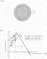
- FIG. 1 is a cross-sectional view of a Cu core ball 1 according to an embodiment of this invention.
- the Cu core ball 1 according to this invention includes a Cu ball (core) 2 having a predetermined size, and a solder layer (covering layer) 3 coating the Cu ball 2.
- the Cu ball 2 provides a space between a semiconductor package (joining object) and a printed circuit board (object to be joined).
- Cu core ball 1 lightness and yellowness prior to heating storage test
- the Cu core ball 1 has, prior to a heating storage test, lightness greater than or equal to 65 in the L*a*b* color space and yellowness less than or equal to 7.0 in the L*a*b* color space.
- a thickness of an oxide film formed on a surface of the solder layer 3A can be managed so as to be a fixed value or less.
- the thickness of the oxide film on the Cu core ball 1 is managed by both indexes of the yellowness and lightness, because the thickness of the oxide film on the Cu core ball 1 cannot be managed accurately by only one index of either yellowness or lightness.
- the thickness of the oxide film on the Cu core ball 1 cannot be managed by yellowness only.
- FIG. 2 is a graph of an oxide film thickness - yellowness (b* value) relationship in the Cu core ball 1 and a solder ball.
- a vertical axis indicates the yellowness
- a horizontal axis indicates the oxide film thickness.
- the oxide film thickness can be managed by the yellowness up to a certain thickness, in case of a solder ball.
- the oxide film thickness is 4nm when the yellowness is 7.2, and the oxide film thickness is 8.7nm when the yellowness is 2.9. Therefore, any correlation is not established between the oxide film thickness and the yellowness. It is conceivable that the impurities in solder plating coating the surface of the Cu ball account for this. Therefore, the index, yellowness, alone may be inadequate for accurate management of the oxide film thickness.
- FIG. 3 is a graph of an oxide film thickness - lightness relationship in the Cu core ball 1 and a solder ball.
- the vertical axis indicates the lightness
- the horizontal axis indicates the thickness of oxide film.
- the thickness of oxide film and the lightness of the Cu core ball 1 are correlated, where the thicker the thickness of oxide film is, the lower the lightness is.
- a correlation coefficient R of the thickness of oxide film and the lightness in this moment has been obtained.
- the correlation coefficient R is obtained from the range of -1 to 1.
- a coefficient of determination R 2 has been obtained by squaring the calculated correlation coefficient.
- the coefficient of determination R 2 is obtained from the range of 0 to 1, and it shows there is a correlation between the thickness of oxide film and lightness when it gets closer to 1.
- the coefficient of determination R 2 of the thickness of oxide film and lightness of the Cu core ball 1 is 0.8229, which is a relatively small number below 1.
- the coefficient of determination R 2 is 0.9523, which shows a value closer to 1, in managing by yellowness. Accordingly, the measured values vary widely in managing by lightness only, and thereby there is a problem that the thickness of oxide film cannot be managed precisely. For this reason, in the present invention, the precise management of the thickness of the oxide film of a Cu core ball 1 prior to the heating storage test is conducted by using the both indexes of the lightness and the yellowness.
- Cu core ball 1 lightness and yellowness subsequent to heating storage test
- the Cu core ball 1 has, subsequent to the heating storage test, lightness greater than or equal to 62.5 in the L*a*b* color space.
- the Cu core ball 1 is heated for 72 hours at 150°C and with atmospheric humidity because the oxide film, which is formed in accordance with the amount of the plating solution residue after cleaning of the Cu core ball 1, may be formed in a short time without a long-term, for example, one-month long storage test.
- the lightness of the Cu core ball 1 to be greater than or equal to 62.5, the Cu core ball 1 having the oxide film thickness greater than a predetermined value (4.9 nm) over the heating storage test may be accurately identified and controlled.
- the lightness of the Cu core ball 1 in the L*a*b* color space may be greater than or equal to 70.2. This may allow for more strict management of the oxide film thickness. By meeting the two requirements, the Cu core ball 1 left with a reduced amount of the plating solution residue after cleaning and less likely to oxidize after long-term storage may be readily identified in a simplified manner.
- the indexes used for thickness management of the oxide film on the Cu core ball 1 subsequent to the heating storage test are described.
- one of the indexes, lightness, alone is used for thickness management of the oxide film because accurate control of the oxide film thickness may be possible with this index.
- thickness management of the oxide film in the Cu core ball 1 may not be possible with the index, yellowness.
- FIG. 4 is a graph of a storage period - yellowness relationship in the Cu core ball 1.
- the vertical axis indicates the yellowness and the horizontal axis indicates the storage period.
- oxidation proceeds more rapidly than that for the conventional solder ball and thereby the yellowness is increased. Afterwards, however, the yellowness is decreased regardless of a prolonged storage period.
- the relationship between the yellowness and the storage period is not proportional.
- the coefficient of determination R 2 of the yellowness and number of storage days is 0.589, which is significantly smaller than 1. Accordingly, the measured values vary widely in managing by yellowness only, and thereby there is a problem that the thickness of oxide film cannot be managed precisely.
- FIG. 4 is a graph of an oxide film thickness - lightness relationship in the Cu core ball 1.
- the vertical axis indicates the lightness and the horizontal axis indicates the oxide film thickness.
- the thickness of oxide film and the lightness of the Cu core ball 1 are correlated, where the thicker the thickness of oxide film is, the lower the lightness is.
- the coefficient of determination R 2 of the lightness and oxide film thickness in the Cu core ball 1 is 0.9332, which shows a value closer to 1. Therefore, lightness-based management may reduce variability of the measured values, allowing for accurate management of the oxide film thickness.
- the lightness-based management alone may result in more variable measured values, failing to accurately management the oxide film thickness of the Cu core ball 1.
- the oxide film thickness of the Cu core ball 1 may be accurately managed by the lightness alone.
- the heating storage test according to this invention is directed to the manufacture of a Cu core ball that may suppress any increase of the oxide film thickness "subsequent to long-term storage".
- the heating storage test therefore, may dispense with the assumption of a number of different oxidation behaviors as in the tests prior to the heating storage test, allowing focus to be placed on oxidation behaviors associated with high-temperature storage alone.
- the heating storage test according to this invention which will be described later in further detail, is performed under uniform conditions including a heating temperature of 150°C or more, except optionally changed heating time, to observe oxidation behaviors associated with high-temperature storage alone. Focusing on the oxidation behaviors associated with high-temperature storage alone, similar growth behaviors of the oxide film thickness may be observed.
- This invention uses one index, lightness, to accurately manage the oxide film thickness of the Cu core ball 1 subsequent to the heating storage test.
- the Cu ball 2 constituting the Cu core ball 1 according to this invention is hereinafter described.
- the properties and other features of the Cu ball 2 remain unchanged before and after the heating storage test, a brief summary of which is given below.
- the Cu ball 2 may desirably be as spherical as possible and less variable in diameter.
- a composition of the Cu ball 2 may be a composition of a single Cu or an alloy composition whose main component is Cu When the Cu ball 2 is composed of an alloy, a content of Cu is equal to or greater than 50 mass %.
- a ball to be cored may be composed of a single metal of Ni, Ag, Bi, Pb, Al, Sn, Fe, Zn, In, Ge, Sb, Co, Mn, Au, Si, Pt, Cr, La, Mo, Nb, Pd, Ti, Zr or Mg besides Cu, or an alloy, a metal oxide, or a mixed metal oxide.
- the purity of the Cu ball 2 is not specifically limited, it is preferably 99.9% or more, from a viewpoint of controlling the alpha dose as necessary and preventing electro-conductivity and/or thermal conductivity of the Cu ball 2 from being deteriorated because of less purity thereof.
- the impurities in the Cu ball 2 may include Sn, Sb, Bi, Ni, Zn, Fe, Al, As, Ag, In, Cd, Pb, Au, P, S, and Co.
- the sphericity is equal to or higher than 0.95, in terms of controlling stand-off height. If the sphericity of the Cu ball 2 is lower than 0.95, the Cu ball 2 becomes into an indeterminate shape. Therefore, bumps having uneven heights are formed at the bump formation time and the possibility that poor joints occur is increased. Moreover, when the Cu core ball 1 is mounted on an electrode and a reflow treatment is performed thereon, there may be a position gap of the Cu core ball 1 and a self-alignment property becomes worse.
- the sphericity is more preferably equal to or higher than 0.990. In the present invention, the sphericity represents a gap from a true sphere.
- the sphericity can be determined by various kinds of methods, for example, a least squares center method (LSC method), a minimum zone center method (MZC method), a maximum inscribed center method (MIC method), a minimum circumscribed center method (MCC method), etc.
- LSC method least squares center method
- MZC method minimum zone center method
- MIC method maximum inscribed center method
- MCC method minimum circumscribed center method
- the sphericity is an arithmetic mean value calculated by dividing a diameter of each of the 500 pieces of the Cu balls 2 by a length of the longest axis of each Cu ball 2. It is shown that when a value thereof is closer to the upper limit 1.00, this is closer to the true sphere.
- the length of the diameter and the length of the longest axis are referred to as lengths measured by measuring equipment, ultra-quick vision, ULTRA QV 350-PRO manufactured by Mitsutoyo Corporation.
- a diameter of the Cu ball 2 is preferably 1-1000 ⁇ m. If the diameter is within this range, the spherical Cu ball 2 can be stably manufactured. Moreover, a shorted connection can be suppressed when a pitch between the terminals is narrow.
- a collection of 'Cu core balls' may be called as 'Cu core powder'.
- the 'Cu core powder' is the collection of many Cu core balls 1, each of which has the property as mentioned above. It is distinguished from a single Cu core ball 1 in usage form, such as it is mixed as the powder in solder paste, for example Similarly, in a case that it is used for forming a solder bump, it is usually treated as a collection, and therefore the 'Cu core powder' used in such a form is distinguished from the single Cu core ball 1.
- solder layer 3 constituting the Cu core ball 1 according to this invention is hereinafter described.
- the properties and other features of the solder layer 3 remain unchanged before and after the heating storage test, a brief summary of which is given below.
- the composition of a solder layer 3 may be a composition of a single Sn, an alloy composition of the lead-free solder alloy whose main component is Sn, or a composition of a Sn-Pb solder alloy.
- a content of Sn is equal to or greater than 40 mass %.
- An alloy element to be added may be, for example, Ag, Cu, In, Ni, Co, Sb, P, Fe, etc.
- an additive amount of alloy element to be added it is preferable that the yellowness and lightness of lead-free solder alloy are reduced to almost the same degree as the yellowness and lightness of the single Sn.
- An alloy composition of the solder layer 3 is preferably Sn-3Ag-0.5 Cu alloy among them, in terms of thermal fatigue life.
- a thickness of the solder layer 3 is not specifically limited: It is, for example, equal to or less than 100 ⁇ m (at each side thereof), which is sufficient. Generally, 20-50 ⁇ m at each side of the layer may be preferable.
- a Sn content of the lead-free solder alloy whose main component is Sn according to the present invention is preferably equal to or more than 80%, and more preferably equal to or more than 90%.
- a layer for coating the Cu ball 2 made of one or more elements selected from Ni and Co, examples of which may include an Ni-plated layer and a Co-plated layer, may be interposed between the solder layer 3 and the surface of the Cu ball 2. This may reduce diffusion of Cu into the solder when joined to electrode, reducing the risk of copper leaching in the Cu ball 2.
- the Ni-plated layer or the Co-plated layer may have a thickness between 0.1 ⁇ m and 20 ⁇ m on one side.
- the Cu core ball 1 may have a flux-coated surface.
- a heat-resistant plate like a ceramic plate, is prepared that has multiple semi-spherical dimples formed on the bottom.
- a diameter of the dimple and a depth thereof are suitably set according to a diameter of the Cu ball 2.
- the diameter thereof is 0.8 mm and the depth thereof is 0.88 mm.
- the Cu materials each having a chip shape hereinafter, referred to as 'chip material'), which are obtained by cutting a fine wire made of Cu, are put into the dimples one by one in the heat-resisting plate.
- the heat-resisting plate in which the chip materials have been put into the dimples is heated at 1100-1300 degrees C in the furnace into which reducing gas such as ammonia decomposition gas is filled and a heating process is performed thereon during 30 through 60 minutes.
- reducing gas such as ammonia decomposition gas
- the chip material is fused so that it becomes sphered.
- the interior of the furnace is cooled and the Cu ball 2 is formed in each of the dimples of the heat-resisting plate.
- the formed Cu ball 2 is reheated at 800 through 1000 degrees C, which is the temperature lower than a melting point of Cu.
- the fused Cu is dropped down from an orifice pierced in a bottom of a melting pot and the droplet is rapidly cooled to be sphered as the Cu ball 2 and a method in which thermal plasma heats cut metal of Cu at a temperature of 1000 degrees C or more to be sphered.
- Each of the Cu ball 2 sphered in such a way may be reheated at about 800 through 1000 degrees C for 30 through 60 minutes.
- the Cu material as a raw material of the Cu ball 2 may be heated at 800 through 1000 degrees C before the Cu ball 2 is sphered.
- the Cu material that is a raw material of the Cu ball 2 for example, pellet, wire, pillar and the like can be used.
- the Cu material may have purity of 99.9%-99.995% from a viewpoint such that the purity in the Cu ball 2 is not too low.
- the heating treatment mentioned above is not performed and a retention temperature of the fused Cu may be lowered to approximately 1000 degrees C as in a conventional way.
- the above-mentioned heating treatment may be omitted or changed according to the purity in the Cu material.
- an electrolytic plating method such as a known barrel plating, a method of generating a high speed turbulent flow in the plating solution within a plating tank by a pump connected to the plating tank and forming the solder layer 3 on the Cu ball 2 by the turbulent flow in the plating solution, a method of providing a vibration plate in a plating tank to vibrate it at predetermined frequency so that the plating solution is agitated by high speed turbulent flow and forming the solder layer 3 on the Cu ball 2 by the turbulent flow in the plating solution and the like.
- solder layer 3 film thickness of a single side of which is 18 ⁇ m
- Ni plating film thickness of a single side of which is 2 ⁇ m
- a Sn-Ag-Cu containing plating solution according to an embodiment of the invention contains a solvent mainly composed of water, sulfonic acids and metal components of Sn, Ag and Cu, as essential components.
- the metal components are present in the plating solution as Sn ions (Sn 2+ and/or Sn 4+ ), Ag ions (Ag + ), and Cu ions (Cu + /Cu + ).
- the plating solution is obtained by mixing plating mother solution mainly composed of water and sulfonic acids with metallic compounds and preferably contains organic complex agent in order to stabilize the metal ions.
- a single species of these Sn compounds can be used or two species or
- Cu compounds copper salts of the above-mentioned organic sulfonic acid, copper sulfate, copper oxide, copper nitrate, copper chloride, copper bromide, copper iodide, copper phosphate, copper pyrophosphate, copper acetate, copper formate, copper citrate, copper gluconate, copper tartrate, copper lactate, copper succinate, copper sulfamate, copper borofluoride, copper silicofluoride and the like are exemplified.
- a single species of these Cu compounds can be used or two species or more thereof can be mixed and used.
- Ag compounds silver salts of the above-mentioned organic sulfonic acid, silver sulfate, silver oxide, silver chloride, silver nitrate, silver bromide, silver iodide, silver phosphate, silver pyrophosphate, silver acetate, silver formate, silver citrate, silver gluconate, silver tartrate, silver lactate, silver succinate, silver sulfamate, silver borofluoride, silver silicofluoride and the like are exemplified.
- a single species of these Ag compounds can be used or two species or more thereof can be mixed and used.
- solder layer 3 film thickness of a single side of which is 20 ⁇ m
- Sn-Ag-Cu solder layer 3 (film thickness of a single side of which is 20 ⁇ m) of Sn-Ag-Cu on the Cu ball 2 having a diameter of 100 ⁇ m
- a quantity of electricity of about 0.0108 coulombs is required.
- Blending quantities of respective metals in the plating solution are as follows: As Sn 2+ , 0.21 through 2 mol/L, preferably 0.25 through 1 mol/L; As Ag + , 0.01 through 0.1 mol/L, preferably 0.02 through 0.05 mol/L and as Cu 2+ , 0.002 through 0.02 mol/L, preferably 0.003 through 0.01 mol/L.
- As Sn 2+ that relates to the plating, a quantity of Sn 2+ may be adjusted in this invention.
- Ag ion concentration to Cu ion concentration is within a range of 4.5 through 5.58. If it stays within this range, it is possible to form the Sn-Ag-Cu based solder layer 3A such as Sn-3Ag-0.5Cu alloy that has a low melting point. Further, a desired deposition amount of solder plating is estimated according to a following formula (1) based on the Faraday's law of electrolysis and an amount of electricity therefor is calculated. The electric current flows through the plating solution so as to be the calculated amount of electricity and the plating is executed while the plating solution flows with the Cu balls 2A.
- a volume of the plating tank may be fixed according to a total input amount of the Cu balls 2A and the plating solution.
- w g I ⁇ t ⁇ M / Z ⁇ F
- "w” is an electrolytic deposition amount (g);
- I is electric current (A);
- t is electricity energizing time (second);
- M is an atomic weight of a deposited element (in a case of Sn, 118.71);
- Z is an atomic value (in a case of Sn, bivalent);
- F is the Faraday constant (96500 coulombs).
- the quantity of electricity Q (A*Sec.) is represented by I ⁇ t.
- the plating has been executed in this invention while the plating solution flows with the Cu balls 2, a flowing method thereof is not particularly limited.
- the plating solution may flow with the Cu balls 2 by a rotation of barrel like the barrel electrolytic plating method.
- any drying is executed in the air or under N 2 atmosphere, so that it is possible to obtain the Cu core ball 1 according to the invention.
- the solder plating performed on the Cu ball 2 may possibly leave residue of the plating solution on the surface of the Cu core ball 1.
- Cleaning is a conventional means to remove the plating solution residue left on the surface of the Cu core ball 1.
- Examples of a cleaning liquid used then may include pure water, organic solvents containing alcohol such as isopropyl alcohol and ketone (acetone), acidic cleaning liquids and basic cleaning liquids containing, for example, trisodium phosphate. Any one of these cleaning liquids may be singly used, or two or more of them may be combined and used.
- cleaning methods employed may include immersion cleaning, ultrasonic cleaning, spray cleaning, shower cleaning, jet cleaning, vacuum cleaning, degassing cleaning, barrel cleaning, brush oscillation cleaning, jet bubble cleaning, and micro-bubble cleaning and the like. Any one of these cleaning methods may be singly used, or two or more of them may be combined and used in accordance with a demanded cleaning effect.
- the amount of the plating solution residue left on the surface of the Cu core ball 1 and the degree of oxidation progress during storage may differ with the cleaning method, cleaning liquid, and cleaning time that are selected and used. Therefore, sufficient cleaning may be a deciding factor in obtaining the Cu core ball 1 less likely oxidize after long-term storage.
- a core constituting the Cu core balls 1 according to this invention can be composed of a resin ball.
- resin materials for example, amino resin, acrylic resin, ethylene-vinyl acetate copolymer, styrene butadiene block copolymer, polyester resin, melamine resin, phenol resin, alkyd resin, polyimide resin, urethane resin, epoxy resin, crosslinked resin are exemplified. It is preferable that especially electro-conductive plastic such as polyacetylene, polypyrrole, polythiophene, polyaniline or the like is used.
- a Cu core ball can be composed of a resin ball and a Sn-Ag-Cu based solder plating layer (covering layer) covering the surface of the resin ball.
- a kind or a layered structure of the covering layer mentioned above is not limited to the examples mentioned above.
- the degree of oxidation progress of the Cu core ball 1 is controlled based on the lightness and yellowness.
- the thickness of the oxide film formed on the surface of the Cu core ball may be directly controlled to determine the degree of oxidation progress of the Cu core ball after cleaning.
- Another example of the Cu core ball according to this embodiment includes a Cu ball that provides a space between a semiconductor package and a printed circuit board, and a solder layer coating the Cu ball. In this Cu core ball, an oxide film thickness subsequent to the heating storage test performed for 72 hours at 150°C and with atmospheric humidity is less than or equal to 4.9 nm.
- a Cu core ball sufficiently cleaned and less likely to oxidize may be identified and obtained.
- the oxide film thickness of the Cu core ball may be, more preferably, less than or equal to 3.1 nm. Any features of this Cu core ball substantially identical to the features of the Cu core ball 1 are not described herein again.
- the soldering material has a ball-like shape.
- This invention is also applicable to a soldering material in the form of a column.
- a soldering material may include a cylindrical column, and a solder layer coating the surface of the cylindrical column.
- This soldering material has lightness greater than or equal to 62.5 in the L*a*b* color space subsequent to the heating storage test performed for 72 hours at 150°C and with atmospheric humidity. Prior to the heating storage test, the soldering material has lightness greater than or equal to 65 in the L*a*b* color space and yellowness less than or equal to 7.0 in the L*a*b* color space.
- the column may be made of a metal selected from Cu, Ni, Ag, Bi, Pb, Al, Sn, Fe, Zn, In, Ge, Sb, Co, Mn, Au, Si, Pt, Cr, La, Mo, Nb, Pd, Ti, Zr, and Mg, or an alloy, a metal oxide, or a mixed metal oxide of any one(s) of these metals, or a resin material.
- the composition of a solder layer may be a composition of a single Sn, an alloy composition of the lead-free solder alloy whose main component is Sn, or a composition of a Sn-Pb solder alloy. When the solder layer is composed of an alloy, a content of Sn is equal to or greater than 40 mass %.
- composition of the lead-free solder for example, Sn, Sn-Ag alloy, Sn-Cu alloy, Sn-Bi alloy, Sn-Ag-Cu alloy, Sn-In alloy and an alloy in which a predetermined alloy element is added to them are exemplified.
- An alloy element to be added may be, for example, Ag, Cu, In, Ni, Co, Sb, P, Fe, etc. Any other features of this soldering material but its shape (sphericity) are substantially identical to the Cu core ball 1, which are not described herein again.
- the Cu core ball 1 according to this invention may be used to form a solder joint for electronic components.
- the solder joint described herein may refer to a structure in which a solder bump is mounted on electrode of a printed circuit board.
- the solder bump described herein may refer to a structure in which the Cu core ball 1 is mounted on electrode of a semiconductor chip.
- Cu wires each having a purity of 99.995% or less were prepared. They were respectively put into the melting pot, the temperature of the melting pot was then risen to 1200 degrees C and this heating treatment was performed during 45 minutes. Subsequently, the fused Cu was dropped down from an orifice pierced through a bottom of the melting pot and the dropped droplet was cooled so as to be manufactured as the Cu ball having a mean diameter of 100 ⁇ m.
- the sphericity of the manufactured Cu ball was measured using CNC image measurement system. Specifically, the ultra quick vision, ULTRA QV350-PRO manufactured by MITSUTOYO Corporation was used. In the executed examples, a length of the longest axis and the diameter of the Cu ball were measured by the measuring equipment mentioned above, and the sphericity was obtained by calculating an arithmetic mean value which was calculated by dividing diameters of 500 Cu balls by their longest axes. It is shown that when a value thereof is closer to the upper limit of 1.00, this is closer to the true ball.
- Cu core ball oxide film thickness, lightness, and yellowness prior to heating storage test
- an Ni-plated layer of 2 ⁇ m in thickness (one side) was formed on the surface of each Cu ball of 100 ⁇ m in diameter to obtain an Ni-plated Cu ball of 104 ⁇ m in diameter.
- a solder layer of 18 ⁇ m in thickness was formed on the surface of each Ni-plated layer to obtain a Cu core ball of 140 ⁇ m in diameter.
- the solder layer was made of an Sn-3 AG-0.5 Cu alloy.
- the obtained Cu core balls were put in a beaker filled with pure water and stirred with a stirrer for 10 minutes, and then cleaned.
- the oxide film thickness, lightness, and yellowness in the respective Cu core balls were measured under different conditions defined in the respective executed examples and comparison examples below.
- the Cu core balls immediately after cleaning was used.
- a Cu core ball was stored in a normal temperature (air exposure) with the humidity of 30% through 40% for 2 days.
- a stirred and cleaned Cu core ball was stored in a normal temperature with the humidity of 30% through 40% for 5 days.
- a stirred and cleaned Cu core ball was stored in a normal temperature with the humidity of 30% through 40% for 7 days.
- a stirred and cleaned Cu core ball was stored in a normal temperature with the humidity of 30% through 40% for 10 days.
- a stirred and cleaned Cu core ball was stored in a normal temperature with the humidity of 30% through 40% for 14 days.
- a stirred and cleaned Cu core ball was stored in the temperature of 40 degrees C with the humidity of 90% for 1 day.
- a stirred and cleaned Cu core ball was stored in a normal temperature with the humidity of 30% through 40% for 20 days.
- a stirred and cleaned Cu core ball was stored at the temperature of 40 degrees C with the humidity of 90% for 2 days.
- a stirred and cleaned Cu core ball was stored at the temperature of 200 degrees C for 1 hour.
- a normal temperature means 20 degrees C through 30 degree C.
- a stirred and cleaned Cu core ball was stored at the temperature of 40 degrees C with the humidity of 90% for 5 days.
- a stirred and cleaned Cu core ball was stored at the temperature of 40 degrees C with the humidity of 90% for 7 days.
- a stirred and cleaned Cu core ball was stored at the temperature of 40 degrees C with the humidity of 90% for 10 days.
- a stirred and cleaned Cu core ball was stored at the temperature of 40 degrees C with the humidity of 90% for 14 days.
- a stirred and cleaned Cu core ball was stored at the temperature of 200 degrees C for 1 day.
- a stirred and cleaned Cu core ball was stored at the temperature of 200 degrees C for 2 days.
- each of the Cu core balls which had been stored under the conditions mentioned above in the executed examples 1 through 10 and the comparison examples 1 through 6 was collected and then lightness, yellowness, and thickness of oxide film of each of the collected Cu core balls were measured, respectively.
- the lightness and the yellowness of each of the Cu core balls were measured with the use of CM-2600d Spectrophotometer manufactured by Konica Minolta.
- the thickness of the oxide film of each of the Cu balls was measured by FE-AES of ULVAC PHI700.
- An acceleration voltage of the measuring apparatus is 10kV and an irradiation current is 10nA.
- the thickness of the oxide film was obtained by a speed of etching the surface of the sample with an Ar ion gun (etching rate), and an etching depth which is 1/2 peak value of oxygen-originated Intensity was used as an approximate value of the oxide film thickness.
- An etching rate is a SiO 2 conversion value obtained by converting a standard sample with etching speed.
- Table 1 shows a relationship among the lightness, yellowness and thickness of oxide film of the measured Cu core ball in each of the executed examples 1 through 10 and the comparison examples 1 through 6. In Table 1, a unit of the thickness of oxide film is (nm).
- the oxide film thickness was 3.8 nm or less in the Cu core balls having the lightness of 62.5 or more and the yellowness of 7.0 or less. As in the executed examples 1 to 5 of Table 1, the oxide film thickness was 1.9 nm in the Cu core balls having the yellowness of 5.1 or less and the lightness of 70 or more. This is smaller than values of the oxide film thickness in the executed examples 6 to 10.
- the oxide film thickness was 3.9 nm or more in the Cu core balls having the lightness of less than 62.5 and the yellowness of more than 7.0. This is greater than a target value of the oxide film thickness. It is known from the result that the oxide film may be smaller in thickness in the core Cu balls having the lightness of 65 or more and the yellowness of 7.0 or less.
- the redness (a* value) was also measured, however, it has been confirmed that the redness cannot be used as an index for managing the thickness of oxide film because the redness was smaller than the correlation coefficient with the thickness of oxide film and contribution ratio 1.
- the alpha dose of each of the Cu core balls in the executed examples 1 through 10 was measured. However, although the result is not shown in the above-mentioned Tables, the alpha dose of each of the Cu core balls was equal to or less than 0.0010cph/cm 2 , which did not reach the required amount of 0.0200 cph/cm 2 .
- Cu core ball oxide film thickness, lightness, and yellowness subsequent to heating storage test
- the heating storage test was performed on the pre-test Cu core balls of the executed example 1 to quickly render the Cu core balls into a condition after long-term storage. Then, the oxide film thickness, lightness, and yellowness of the Cu core balls subsequent to the heating storage test were measured. The Cu core balls used then had been stirred and cleaned for 10 minutes, as mentioned above.
- a temperature-controlled bath was set to and kept at 150°C for more than one hour.
- An executed example 1A cleaned again the Cu core balls, which had been stirred and cleaned, using a first cleaning method, and stored the cleaned Cu core balls in the temperature-controlled bath at 150°C for three days.
- An executed example 1B cleaned again the Cu core balls, which had been stirred and cleaned, using a second cleaning method, and stored the cleaned Cu core balls in the temperature-controlled bath at 150°C for three days.
- An executed example 1C cleaned again the Cu core balls, which had been stirred and cleaned, using a third cleaning method, and stored the cleaned Cu core balls in the temperature-controlled bath at 150°C for three days.
- a comparison example 1A stored the Cu core balls, which had been stirred and cleaned, in the temperature-controlled bath at 150°C for three days.
- the Cu core balls were put in a beaker filled with pure water, and the beaker containing the Cu core balls was set in an ultrasonic cleaner and subjected to ultrasonic cleaning for 10 seconds.
- the Cu core balls were put in a beaker filled with pure water, and the beaker containing the Cu core balls was set in an ultrasonic cleaner and subjected to ultrasonic cleaning for 60 seconds.
- the Cu core balls were put in a beaker filled with pure water, and the beaker containing the Cu core balls was set in an ultrasonic cleaner and subjected to ultrasonic cleaning for 180 seconds.
- the first to third cleaning methods were ranked as methods of a high cleaning effect that may adequately remove residue of the plating solution.
- the stirring and cleaning alone were ranked as a method of a poor cleaning effect that may fail to adequately remove residue of the plating solution.
- each of the Cu core balls which had been cleaned and heat-stored under the conditions mentioned above in the executed examples 1A, 1B, 1C and the comparison example 1A was collected and then lightness, yellowness, and thickness of oxide film of each of the collected Cu core balls were measured, respectively.
- the lightness and the yellowness of each of the Cu core balls were measured with the use of CM-2600d Spectrophotometer manufactured by Konica Minolta.
- the thickness of the oxide film of each of the Cu balls was measured by FE-AES of ULVAC PHI700.
- An acceleration voltage of the measuring apparatus is 10kV and an irradiation current is 10nA.
- the thickness of the oxide film was obtained by a speed of etching the surface of the sample with an Ar ion gun (etching rate), and an etching depth which is 1/2 peak value of oxygen-originated Intensity was used as an approximate value of the oxide film thickness.
- An etching rate is a SiO 2 conversion value obtained by converting a standard sample with etching speed.
- Table 2 shows a relationship among the lightness, yellowness and thickness of oxide film of the measured Cu core ball in each of the executed examples 1A, 1B, 1C and the comparison example 1A. In Table 2, a unit of the thickness of oxide film is (nm).
- the stirring and cleaning alone resulted in the Cu core balls having the lightness of less than 62.5 and the oxide film thickness of more than 4.9 nm after the heating storage test.
- This result teaches that the Cu core balls having the lightness of less than 62.5 after the heating and storage, if selected, may be left with residue of the solder plating solution in rather abundance due to insufficient cleaning and likely to oxidize after long-term storage (thick oxide film).
- the Cu core balls of the executed example 1 in Table 1 were used, which is a non-limiting example.
- the Cu core balls of the executed examples 2 to 10 in Table 1 were found to obtain similar effects to the Cu core balls of the executed example 1, though it is not shown in Table 1.
- these Cu core balls had the lightness of 62.5 or more, and the oxide film thickness of 4.9 nm or less.
- Table 3 shows a relationship among the lightness, yellowness, and oxide film thickness in the Cu core balls immediately after cleaning before they were heated and stored.
- a unit of the thickness of oxide film is (nm).
- the Cu core balls immediately after cleaning and before the heating storage test had the lightness of 71.2 or more and the oxide film thickness of 1.2 nm or less.
- the oxide film growth that depends on residue of the plating solution may not be facilitated immediately after cleaning and before the heating storage test, and values of the oxide film thickness may not be so different among the different cleaning conditions.
- Table 4 shows a relationship among the lightness, yellowness, and oxide film thickness in the Cu core balls subjected to the heating storage test at 150°C for five days (120 hours).
- a unit of the thickness of oxide film is (nm).
- Storage conditions heating temperature/number of storage days)
- Cleaning conditions Reference example 5 57.1 3.1 8.1 150°C/5 days Stirring and cleaning + ultrasonic cleaning for 10 sec.
- Reference example 6 60.7 4.7 6.1 150°C/5 days Stirring and cleaning + ultrasonic cleaning for 60 sec.
- the Cu core balls had the lightness of 57.1 or more and the oxide film thickness of 8.1 nm or less.
- the stirring and cleaning alone resulted in the Cu core balls having the lightness of less than 57.1 and the oxide film thickness of more than 8.1 nm after the heating storage test.
- Table 5 shows a relationship among the lightness, yellowness, and oxide film thickness in the Cu core balls subjected to the heating storage test at 150°C for seven days (168 hours).
- a unit of the thickness of oxide film is (nm).
- Storage conditions heating temperature/numb er of storage days)
- Cleaning conditions Reference example 9 53.9 1.3 11.5 150°C/7 days Stirring and cleaning + ultrasonic cleaning for 10 sec.
Landscapes
- Engineering & Computer Science (AREA)
- Chemical & Material Sciences (AREA)
- Mechanical Engineering (AREA)
- Physics & Mathematics (AREA)
- Organic Chemistry (AREA)
- Materials Engineering (AREA)
- Metallurgy (AREA)
- Life Sciences & Earth Sciences (AREA)
- Health & Medical Sciences (AREA)
- Analytical Chemistry (AREA)
- Biochemistry (AREA)
- General Health & Medical Sciences (AREA)
- General Physics & Mathematics (AREA)
- Immunology (AREA)
- Pathology (AREA)
- Chemical Kinetics & Catalysis (AREA)
- Nanotechnology (AREA)
- Thermal Sciences (AREA)
- Manufacturing & Machinery (AREA)
- Microelectronics & Electronic Packaging (AREA)
- Inorganic Chemistry (AREA)
- Spectroscopy & Molecular Physics (AREA)
- Powder Metallurgy (AREA)
- Electric Connection Of Electric Components To Printed Circuits (AREA)
Abstract
Description
- This invention relates to a soldering material, a solder joint, and a soldering material inspecting method.
- In tandem with the development of compact Information appliances in recent years, there is a rapid ongoing progress in miniaturization of electronic components to be mounted on such appliances. The technique called, ball grid array (hereinafter, "BGA") with an electrode-mounted back surface, may be applied to the electronic components to fulfill the needs for miniaturization, for example, smaller connection terminals and narrower-pitched mounting area.
- Examples of the BGA-applied electronic components may include semiconductor packages. For example, the semiconductor package may have a structure in which electrode-mounted semiconductor chips are joined with solder bumps to the conductive land of a printed circuit board and then sealed in resin. In recent years, a three-dimensional high-density mounting has been developed by stacking up the semiconductor packages in a height direction in order to meet the further high-density mounting requirement.
- Examples of the solder bumps so far developed may include Cu core balls.
Patent Document 1 describes a Cu core ball including a Cu ball as its core and a solder layer coating the Cu ball's surface. The solder bump formed by using the Cu core ball can support a semiconductor package by the Cu ball, which is not melted at a melting temperature of the solder, even if the solder bump receives the weight of the semiconductor package when the electronic components are mounted on the printed circuit board. Therefore, it can be prevented that the solder bump is crushed by the semiconductor package's weight. - By the way, there is an occasion when an oxide film is formed on a solder surface of the Cu core ball. By this influence of the oxide film, wettability defects occur between the solder and an electrode. As the result, a mounting failure of the Cu core ball occurs, and therefore a problem that the productivity or yield ratio of the semiconductor package is significantly decreased arises. Accordingly, the Cu core ball should desirably be resistant to oxidation.
- There is also an occasion when a problem of oxide film of the Cu core ball arises due to the temperature or humidity of the storage environment of the Cu core ball after being manufactured. Even in a case where a reflow treatment is conducted after mounting a Cu core ball having an oxide film formed on the electrodes of the semiconductor package, wettability defects of solder occurs similarly, and the solder constituting the Cu core ball does not wetly spread across the entire electrode. Accordingly, there is a problem that a mounting failure of the Cu core ball occurs because of the electrode exposure, misaligned Cu core ball toward the electrodes or the like. Therefore, the management of oxide film thickness after manufacturing Cu core balls is also an important problem.
- The inventors of this application focused on two indexes; yellowness and lightness, for the management of oxide film thickness before the solder starts to melt. Then, the inventors have suggested that the thickness of the oxide film formed on the surface of the solder material can be managed accurately, by selecting any Cu core ball having yellowness and lightness that respectively fall within ranges of preset values. By using Cu core balls obtained by the management of oxide film thickness, semiconductor chips may be effectively joined to a printed circuit board.
- Patent Document 1: International Patent Publication No.
95/24113 - Conventionally, a plating treatment performed on the Cu ball is followed by cleaning to remove residue of a plating solution, for example, components of the plating solution left on the surface of the Cu core ball. Examples of the residue may include organic complexing agent, pH regulator, pH buffer, accelerator, stabilizer, surface active agent, brightening agent, semi-brightening agent, and lubricating agent. However, even for the Cu core ball having yellowness and lightness that respectively fall within ranges of preset values after manufacturing, in case the cleaning is insufficient, the plating solution residue may be left in rather abundance on the surface of the Cu core ball. Then, long-term storage, even if optimally conditioned, may accelerate more than usual the solder's oxidation on the surface of the Cu core ball depending on the amount of residue. As a result, this may occur with any Cu core balls having yellowness and lightness that respectively fall within ranges of preset values after the manufacture. The yellowness and lightness of a manufactured Cu core ball selected and used may meet the preset numerical ranges. Yet, the oxide film is still possibly formed on the surface of this Cu core ball, which may result in bonding failure at the time of joining a semiconductor chip to a printed circuit board.
- To address these issues of the known art, this invention is directed to providing a soldering material less likely to oxidize after long-term storage, and a solder joint using the soldering material. This invention is further directed to providing a soldering material inspecting method for accurately identifying a soldering material less likely to oxidize after long-term storage.
- The inventors' finding is, when lightness (L*value) in the L*a*b* color space subsequent to a heating storage test is greater than or equal to 62.5 in a Cu core ball cleaned and then heated at a predetermined temperature and with atmospheric humidity to purposely accelerate the oxidation, the Cu core ball may have a reduced amount of the plating solution residue, i.e., the Cu core ball may be less likely to oxidize. The heating storage test described herein refers to a test performed to purposely accelerate the growth of an oxide film on a Cu core ball formed in accordance with the amount of plating solution residue after cleaning of the
Cu core ball 1. In this test, the formed Cu core ball may be, for example, heated and stored for 72 hours in a temperature-controlled bath at 150°C with a temperature of 25°C and 40% humidity. Some of the Cu core balls manufactured may be subjected to an acceleration test. - (1) This invention provides a soldering material including: a core that provides a space between a joining object and an object to be joined; and a covering layer coating the core and including Sn or a solder alloy primarily consisting of Sn. The soldering material has lightness greater than or equal to 62.5 in L*a*b* color space subsequent to a heating storage test performed for 72 hours in a temperature-controlled bath at 150°C with a temperature of 25°C and 40% humidity. The soldering material prior to the heating storage test has lightness greater than or equal to 65 in the L*a*b* color space and yellowness less than or equal to 7.0 in the L*a*b* color space.
- (2) The soldering material recited in the above-mentioned item (1) may be further characterized in that the core is coated with a layer including one or more elements selected from the group consisting of Ni and Co, and is then coated with the solder layer.
- (3) The soldering material recited in the above-mentioned item (1) or (2) may be further characterized in that the lightness of the soldering material in the L*a*b* color space subsequent to the heating storage test is greater than or equal to 70.2.
- (4) The soldering material recited in any one of the above-mentioned items (1) through (3) may be further characterized in that the core is a spherical material made of at least one element selected from the group consisting of Cu, Ni, Ag, Bi, Pb, Al, Sn, Fe, Zn, In, Ge, Sb, Co, Mn, Au, Si, Pt, Cr, La, Mo, Nb, Pd, Ti, Zr, and Mg, or a resin material.
- (5) The soldering material recited in any one of the above-mentioned items (1) through (3) may be further characterized in that the core is a cylindrical material made of at least one element selected from the group consisting of Cu, Ni, Ag, Bi, Pb, Al, Sn, Fe, Zn, In, Ge, Sb, Co, Mn, Au, Si, Pt, Cr, La, Mo, Nb, Pd, Ti, Zr, and Mg, or a resin material.
- (6) A solder joint using any one of the soldering materials recited in the above-mentioned items (1) through (5).
- (7) This invention further provides a soldering material including: a core that provides a space between a joining object and an object to be joined; and a covering layer coating the core and including Sn or a solder alloy primarily consisting of Sn. In this soldering material, an oxide film thickness is less than or equal to 4.9 nm subsequent to heating for 72 hours in a temperature-controlled bath at 150°C with a temperature of 25°C and 40% humidity.
- (8) The soldering material recited in the above-mentioned item (7) may be further characterized in that the core is coated with a layer including one or more elements selected from the group consisting of Ni and Co, and is then coated with the solder layer.
- (9) The soldering material recited in the above-mentioned item (7) or (8) may be further characterized in that the oxide film thickness is less than or equal to 3.1 nm subsequent to the heating storage test.
- (10) The soldering material recited in any one of the above-mentioned items (7) through (9) may be further characterized in that the core is a spherical material made of at least one element selected from the group consisting of Cu, Ni, Ag, Bi, Pb, Al, Sn, Fe, Zn, In, Ge, Sb, Co, Mn, Au, Si, Pt, Cr, La, Mo, Nb, Pd, Ti, Zr, and Mg, or a resin material.
- (11) The soldering material recited in any one of the above-mentioned items (7) through (9) may be further characterized in that the core is a cylindrical material made of at least one element selected from the group consisting of Cu, Ni, Ag, Bi, Pb, Al, Sn, Fe, Zn, In, Ge, Sb, Co, Mn, Au, Si, Pt, Cr, La, Mo, Nb, Pd, Ti, Zr, and Mg, or a resin material.
- (12) A solder joint using any one of the soldering materials recited in the above-mentioned items (7) through (11).
- (13) This invention further provides a soldering material inspecting method, including steps of: heating a soldering material for 72 hours in a temperature-controlled bath at 150°C with a temperature of 25°C and 40% humidity, the soldering material including a core that provides a space between a joining object and object to be joined, and a covering layer coating the core and including Sn or a solder alloy primarily consisting of Sn; and obtaining the soldering material having lightness greater than or equal to 62.5 in L*a*b* color space subsequent to the heating step.
- The soldering material, solder joint, and soldering material inspecting method according to this invention may allow Cu core balls less likely to oxidize after long-term storage to be accurately identified in a short time.
-
- [
FIG.1] FIG. 1 is a cross-sectional view of a Cu core ball according to an embodiment of the present invention for showing a configuration example thereof. - [
FIG. 2] FIG. 2 is a graph of an oxide film thickness - yellowness relationship in a Cu core ball prior to a heating storage test. - [
FIG. 3] FIG. 3 is a graph of an oxide film thickness - lightness relationship in a Cu core ball prior to the heating storage test. - [
FIG. 4] FIG. 4 is a graph of a storage period - yellowness relationship in a Cu core ball subsequent to the heating storage test. - [
FIG. 5] FIG. 5 is a graph of an oxide film thickness - lightness relationship in a Cu core ball subsequent to the heating storage test. - A preferred embodiment of this invention is hereinafter described in detail referring to the accompanying drawings. The terms, lightness and yellowness, hereinafter described refer to the L*a*b* color space.
-
FIG. 1 is a cross-sectional view of aCu core ball 1 according to an embodiment of this invention. As illustrated inFIG. 1 , theCu core ball 1 according to this invention includes a Cu ball (core) 2 having a predetermined size, and a solder layer (covering layer) 3 coating theCu ball 2. TheCu ball 2 provides a space between a semiconductor package (joining object) and a printed circuit board (object to be joined). - The
Cu core ball 1 according to this invention has, prior to a heating storage test, lightness greater than or equal to 65 in the L*a*b* color space and yellowness less than or equal to 7.0 in the L*a*b* color space. By selecting theCu core ball 1 having lightness and yellowness meeting these numerical ranges, a thickness of an oxide film formed on a surface of the solder layer 3A can be managed so as to be a fixed value or less. - In this invention, prior to the heating storage test, the thickness of the oxide film on the
Cu core ball 1 is managed by both indexes of the yellowness and lightness, because the thickness of the oxide film on theCu core ball 1 cannot be managed accurately by only one index of either yellowness or lightness. Hereinafter is described why the thickness of the oxide film on theCu core ball 1 cannot be managed by yellowness only. -
FIG. 2 is a graph of an oxide film thickness - yellowness (b* value) relationship in theCu core ball 1 and a solder ball. In the graph, a vertical axis indicates the yellowness and a horizontal axis indicates the oxide film thickness. As illustrated inFIG. 2 , as for the solder ball, the thicker the oxide film thickness on the surface is, the more the yellowness rises.. Thus, the yellowness and oxide film thickness of the solder ball are substantially in proportional relation to each other. Therefore, the oxide film thickness can be managed by the yellowness up to a certain thickness, in case of a solder ball. - Whereas, as for the
Cu core ball 1, oxidation proceeds more rapidly than that for the solder ball and thereby the yellowness is increased. Afterwards, however, the yellowness is decreased regardless of the increase of the oxide film thickness. The relationship between the oxide film thickness and the yellowness is not proportional For example, the oxide film thickness is 4nm when the yellowness is 7.2, and the oxide film thickness is 8.7nm when the yellowness is 2.9. Therefore, any correlation is not established between the oxide film thickness and the yellowness. It is conceivable that the impurities in solder plating coating the surface of the Cu ball account for this. Therefore, the index, yellowness, alone may be inadequate for accurate management of the oxide film thickness. - The following will describe a reason why the thickness of the oxide film on the
Cu core ball 1 cannot be managed by lightness only.FIG. 3 is a graph of an oxide film thickness - lightness relationship in theCu core ball 1 and a solder ball. In the graph, the vertical axis indicates the lightness and the horizontal axis indicates the thickness of oxide film. As illustrated inFIG. 3 , the thickness of oxide film and the lightness of theCu core ball 1 are correlated, where the thicker the thickness of oxide film is, the lower the lightness is. A correlation coefficient R of the thickness of oxide film and the lightness in this moment has been obtained. The correlation coefficient R is obtained from the range of -1 to 1. Subsequently, a coefficient of determination R2 has been obtained by squaring the calculated correlation coefficient. The coefficient of determination R2 is obtained from the range of 0 to 1, and it shows there is a correlation between the thickness of oxide film and lightness when it gets closer to 1. - The coefficient of determination R2 of the thickness of oxide film and lightness of the
Cu core ball 1 is 0.8229, which is a relatively small number below 1. Whereas, when a coefficient of determination of the thickness of oxide film and yellowness is obtained by the above-mentioned method, with the use of the values only before the yellowness's decreased shown in theFIG. 2 , the coefficient of determination R2 is 0.9523, which shows a value closer to 1, in managing by yellowness. Accordingly, the measured values vary widely in managing by lightness only, and thereby there is a problem that the thickness of oxide film cannot be managed precisely. For this reason, in the present invention, the precise management of the thickness of the oxide film of aCu core ball 1 prior to the heating storage test is conducted by using the both indexes of the lightness and the yellowness. - The
Cu core ball 1 according to this invention has, subsequent to the heating storage test, lightness greater than or equal to 62.5 in the L*a*b* color space. TheCu core ball 1 is heated for 72 hours at 150°C and with atmospheric humidity because the oxide film, which is formed in accordance with the amount of the plating solution residue after cleaning of theCu core ball 1, may be formed in a short time without a long-term, for example, one-month long storage test. By defining the lightness of theCu core ball 1 to be greater than or equal to 62.5, theCu core ball 1 having the oxide film thickness greater than a predetermined value (4.9 nm) over the heating storage test may be accurately identified and controlled. The lightness of theCu core ball 1 in the L*a*b* color space may be greater than or equal to 70.2. This may allow for more strict management of the oxide film thickness. By meeting the two requirements, theCu core ball 1 left with a reduced amount of the plating solution residue after cleaning and less likely to oxidize after long-term storage may be readily identified in a simplified manner. - Hereinafter are described the indexes used for thickness management of the oxide film on the
Cu core ball 1 subsequent to the heating storage test. In theCu core ball 1 subsequent to the heating storage test, one of the indexes, lightness, alone is used for thickness management of the oxide film because accurate control of the oxide film thickness may be possible with this index. Hereinafter is described why thickness management of the oxide film in theCu core ball 1 may not be possible with the index, yellowness. -
FIG. 4 is a graph of a storage period - yellowness relationship in theCu core ball 1. In the graph, the vertical axis indicates the yellowness and the horizontal axis indicates the storage period. As for theCu core ball 1, oxidation proceeds more rapidly than that for the conventional solder ball and thereby the yellowness is increased. Afterwards, however, the yellowness is decreased regardless of a prolonged storage period. The relationship between the yellowness and the storage period is not proportional. On and after one-day storage of theCu core ball 1, The coefficient of determination R2 of the yellowness and number of storage days is 0.589, which is significantly smaller than 1. Accordingly, the measured values vary widely in managing by yellowness only, and thereby there is a problem that the thickness of oxide film cannot be managed precisely. - Hereinafter is described why thickness management of the oxide film in the
Cu core ball 1 may be possible with the index, lightness, alone.FIG. 4 is a graph of an oxide film thickness - lightness relationship in theCu core ball 1. In the graph, the vertical axis indicates the lightness and the horizontal axis indicates the oxide film thickness. The thickness of oxide film and the lightness of theCu core ball 1 are correlated, where the thicker the thickness of oxide film is, the lower the lightness is. The coefficient of determination R2 of the lightness and oxide film thickness in theCu core ball 1 is 0.9332, which shows a value closer to 1. Therefore, lightness-based management may reduce variability of the measured values, allowing for accurate management of the oxide film thickness. - Prior to the heating storage test, the lightness-based management alone may result in more variable measured values, failing to accurately management the oxide film thickness of the
Cu core ball 1. After the heating storage test, on the other hand, the oxide film thickness of theCu core ball 1 may be accurately managed by the lightness alone. These different approaches before and after the test may be possible because of the reason described below. Tests performed prior to the heating storage test, which will be described later in further detail, are directed to the manufacture of a Cu core ball that may suppress any increase of the oxide film thickness by mounting the Cu core ball immediately after the manufacture in any possible oxidation behaviors assumed under different test conditions including temperature, humidity, and heating time. - The heating storage test according to this invention is directed to the manufacture of a Cu core ball that may suppress any increase of the oxide film thickness "subsequent to long-term storage". The heating storage test, therefore, may dispense with the assumption of a number of different oxidation behaviors as in the tests prior to the heating storage test, allowing focus to be placed on oxidation behaviors associated with high-temperature storage alone. The heating storage test according to this invention, which will be described later in further detail, is performed under uniform conditions including a heating temperature of 150°C or more, except optionally changed heating time, to observe oxidation behaviors associated with high-temperature storage alone. Focusing on the oxidation behaviors associated with high-temperature storage alone, similar growth behaviors of the oxide film thickness may be observed. Similar growth behaviors of the oxide film thickness may lead to similar changes of the lightness, which indicates an improved correlation between the lightness and oxide film thickness. This invention, therefore, uses one index, lightness, to accurately manage the oxide film thickness of the
Cu core ball 1 subsequent to the heating storage test. - The
Cu ball 2 constituting theCu core ball 1 according to this invention is hereinafter described. The properties and other features of theCu ball 2 remain unchanged before and after the heating storage test, a brief summary of which is given below. When theCu core ball 1 is used for a solder bump, theCu ball 2 is not meltable at soldering temperatures, serving to suppress the variability of a solder joint in height. Therefore, theCu ball 2 may desirably be as spherical as possible and less variable in diameter. - A composition of the
Cu ball 2 may be a composition of a single Cu or an alloy composition whose main component is Cu When theCu ball 2 is composed of an alloy, a content of Cu is equal to or greater than 50 mass %. In addition, a ball to be cored may be composed of a single metal of Ni, Ag, Bi, Pb, Al, Sn, Fe, Zn, In, Ge, Sb, Co, Mn, Au, Si, Pt, Cr, La, Mo, Nb, Pd, Ti, Zr or Mg besides Cu, or an alloy, a metal oxide, or a mixed metal oxide. - Although the purity of the
Cu ball 2 is not specifically limited, it is preferably 99.9% or more, from a viewpoint of controlling the alpha dose as necessary and preventing electro-conductivity and/or thermal conductivity of theCu ball 2 from being deteriorated because of less purity thereof. Examples of the impurities in theCu ball 2 may include Sn, Sb, Bi, Ni, Zn, Fe, Al, As, Ag, In, Cd, Pb, Au, P, S, and Co. - For the
Cu ball 2, the sphericity is equal to or higher than 0.95, in terms of controlling stand-off height. If the sphericity of theCu ball 2 is lower than 0.95, theCu ball 2 becomes into an indeterminate shape. Therefore, bumps having uneven heights are formed at the bump formation time and the possibility that poor joints occur is increased. Moreover, when theCu core ball 1 is mounted on an electrode and a reflow treatment is performed thereon, there may be a position gap of theCu core ball 1 and a self-alignment property becomes worse. The sphericity is more preferably equal to or higher than 0.990. In the present invention, the sphericity represents a gap from a true sphere. The sphericity can be determined by various kinds of methods, for example, a least squares center method (LSC method), a minimum zone center method (MZC method), a maximum inscribed center method (MIC method), a minimum circumscribed center method (MCC method), etc. For details, the sphericity is an arithmetic mean value calculated by dividing a diameter of each of the 500 pieces of theCu balls 2 by a length of the longest axis of eachCu ball 2. It is shown that when a value thereof is closer to the upper limit 1.00, this is closer to the true sphere. In this invention, the length of the diameter and the length of the longest axis are referred to as lengths measured by measuring equipment, ultra-quick vision, ULTRA QV 350-PRO manufactured by Mitsutoyo Corporation. - A diameter of the
Cu ball 2 is preferably 1-1000 µm. If the diameter is within this range, thespherical Cu ball 2 can be stably manufactured. Moreover, a shorted connection can be suppressed when a pitch between the terminals is narrow. - Here, for example, if the diameter of the
Cu core ball 1 according to the present invention is about 1-300µm, a collection of 'Cu core balls' may be called as 'Cu core powder'. The 'Cu core powder' is the collection of manyCu core balls 1, each of which has the property as mentioned above. It is distinguished from a singleCu core ball 1 in usage form, such as it is mixed as the powder in solder paste, for example Similarly, in a case that it is used for forming a solder bump, it is usually treated as a collection, and therefore the 'Cu core powder' used in such a form is distinguished from the singleCu core ball 1. - The
solder layer 3 constituting theCu core ball 1 according to this invention is hereinafter described. The properties and other features of thesolder layer 3 remain unchanged before and after the heating storage test, a brief summary of which is given below. When theCu core ball 1 is used for a solder bump, thesolder layer 3 is melted at reflow temperatures to serve as a joining material that electrically joins electrodes of a semiconductor package and of a printed circuit board. - The composition of a
solder layer 3 may be a composition of a single Sn, an alloy composition of the lead-free solder alloy whose main component is Sn, or a composition of a Sn-Pb solder alloy. When thesolder layer 3 is composed of an alloy, a content of Sn is equal to or greater than 40 mass %. As an example of the composition of the lead-free solder, for example, Sn, Sn-Ag alloy, Sn-Cu alloy, Sn-Bi alloy, Sn-Ag-Cu alloy, Sn-In alloy and an alloy in which a predetermined alloy element is added to them are exemplified. An alloy element to be added may be, for example, Ag, Cu, In, Ni, Co, Sb, P, Fe, etc. As for an additive amount of alloy element to be added, it is preferable that the yellowness and lightness of lead-free solder alloy are reduced to almost the same degree as the yellowness and lightness of the single Sn. An alloy composition of thesolder layer 3 is preferably Sn-3Ag-0.5 Cu alloy among them, in terms of thermal fatigue life. A thickness of thesolder layer 3 is not specifically limited: It is, for example, equal to or less than 100µm (at each side thereof), which is sufficient. Generally, 20-50µm at each side of the layer may be preferable. Moreover, a Sn content of the lead-free solder alloy whose main component is Sn according to the present invention is preferably equal to or more than 80%, and more preferably equal to or more than 90%. - Optionally, a layer for coating the
Cu ball 2 made of one or more elements selected from Ni and Co, examples of which may include an Ni-plated layer and a Co-plated layer, may be interposed between thesolder layer 3 and the surface of theCu ball 2. This may reduce diffusion of Cu into the solder when joined to electrode, reducing the risk of copper leaching in theCu ball 2. The Ni-plated layer or the Co-plated layer may have a thickness between 0.1 µm and 20 µm on one side. TheCu core ball 1 may have a flux-coated surface. - Next, the following will describe an example of a method of manufacturing the
Cu core ball 1 according to this invention. First, a heat-resistant plate, like a ceramic plate, is prepared that has multiple semi-spherical dimples formed on the bottom. A diameter of the dimple and a depth thereof are suitably set according to a diameter of theCu ball 2. For example, the diameter thereof is 0.8 mm and the depth thereof is 0.88 mm. Further, the Cu materials each having a chip shape (hereinafter, referred to as 'chip material'), which are obtained by cutting a fine wire made of Cu, are put into the dimples one by one in the heat-resisting plate. - Next, the heat-resisting plate in which the chip materials have been put into the dimples is heated at 1100-1300 degrees C in the furnace into which reducing gas such as ammonia decomposition gas is filled and a heating process is performed thereon during 30 through 60 minutes. In this moment, when temperature in the furnace is more than the melting point of Cu, the chip material is fused so that it becomes sphered. Thereafter, the interior of the furnace is cooled and the
Cu ball 2 is formed in each of the dimples of the heat-resisting plate. After being cooled, the formedCu ball 2 is reheated at 800 through 1000 degrees C, which is the temperature lower than a melting point of Cu. - Further, as other methods, there are an atomizing method in which the fused Cu is dropped down from an orifice pierced in a bottom of a melting pot and the droplet is rapidly cooled to be sphered as the
Cu ball 2 and a method in which thermal plasma heats cut metal of Cu at a temperature of 1000 degrees C or more to be sphered. Each of theCu ball 2 sphered in such a way may be reheated at about 800 through 1000 degrees C for 30 through 60 minutes. In addition, the Cu material as a raw material of theCu ball 2 may be heated at 800 through 1000 degrees C before theCu ball 2 is sphered. - As the Cu material that is a raw material of the
Cu ball 2, for example, pellet, wire, pillar and the like can be used. The Cu material may have purity of 99.9%-99.995% from a viewpoint such that the purity in theCu ball 2 is not too low. - In a case of using a Cu material having the further high purity, the heating treatment mentioned above is not performed and a retention temperature of the fused Cu may be lowered to approximately 1000 degrees C as in a conventional way. Thus, the above-mentioned heating treatment may be omitted or changed according to the purity in the Cu material.
- As the method of forming the
solder layer 3 on theCu ball 2 by flowing the plating solution with theCu balls 2 manufactured as described above, there are an electrolytic plating method such as a known barrel plating, a method of generating a high speed turbulent flow in the plating solution within a plating tank by a pump connected to the plating tank and forming thesolder layer 3 on theCu ball 2 by the turbulent flow in the plating solution, a method of providing a vibration plate in a plating tank to vibrate it at predetermined frequency so that the plating solution is agitated by high speed turbulent flow and forming thesolder layer 3 on theCu ball 2 by the turbulent flow in the plating solution and the like. - The following will describe an example of forming the solder layer 3 (film thickness of a single side of which is 18µm) of Sn-Ag-Cu after coating a Ni plating (film thickness of a single side of which is 2µm) on the
Cu ball 2 having a diameter of 100µm to form theCu core 1 ball having a diameter of about 140µm. - A Sn-Ag-Cu containing plating solution according to an embodiment of the invention contains a solvent mainly composed of water, sulfonic acids and metal components of Sn, Ag and Cu, as essential components.
- The metal components are present in the plating solution as Sn ions (Sn2+ and/or Sn4+), Ag ions (Ag+), and Cu ions (Cu+/Cu+). The plating solution is obtained by mixing plating mother solution mainly composed of water and sulfonic acids with metallic compounds and preferably contains organic complex agent in order to stabilize the metal ions.
- As the metallic compounds in the plating solution, the following ones are exemplified, for instance. As specific examples of the Sn compounds, tin salts of organic sulfonic acid such as methanesulfonic acid, ethanesulfonic acid, 2-propanol sulfonic acid, p-phenolsulfonic acid and the like and stannous compounds such as tin sulfate, tin oxide, tin nitrate, tin chloride, tin bromide, tin iodide, tin phosphate, tin pyrophosphate, tin acetate, tin formate, tin citrate, tin gluconate, tin tartrate, tin lactate, tin succinate, tin sulfamate, tin borofluoride, tin silicofluoride and the like are exemplified. A single species of these Sn compounds can be used or two species or more thereof can be mixed and used.
- As the Cu compounds, copper salts of the above-mentioned organic sulfonic acid, copper sulfate, copper oxide, copper nitrate, copper chloride, copper bromide, copper iodide, copper phosphate, copper pyrophosphate, copper acetate, copper formate, copper citrate, copper gluconate, copper tartrate, copper lactate, copper succinate, copper sulfamate, copper borofluoride, copper silicofluoride and the like are exemplified. A single species of these Cu compounds can be used or two species or more thereof can be mixed and used.
- As the Ag compounds, silver salts of the above-mentioned organic sulfonic acid, silver sulfate, silver oxide, silver chloride, silver nitrate, silver bromide, silver iodide, silver phosphate, silver pyrophosphate, silver acetate, silver formate, silver citrate, silver gluconate, silver tartrate, silver lactate, silver succinate, silver sulfamate, silver borofluoride, silver silicofluoride and the like are exemplified. A single species of these Ag compounds can be used or two species or more thereof can be mixed and used.
- Further, when forming the solder layer 3 (film thickness of a single side of which is 20µm) of Sn-Ag-Cu on the
Cu ball 2 having a diameter of 100µm, a quantity of electricity of about 0.0108 coulombs is required. - Blending quantities of respective metals in the plating solution are as follows: As Sn2+, 0.21 through 2 mol/L, preferably 0.25 through 1 mol/L; As Ag+, 0.01 through 0.1 mol/L, preferably 0.02 through 0.05 mol/L and as Cu2+, 0.002 through 0.02 mol/L, preferably 0.003 through 0.01 mol/L. Here, since it is Sn2+ that relates to the plating, a quantity of Sn2+ may be adjusted in this invention.
- Moreover, it is preferable that Ag ion concentration to Cu ion concentration (Ag/Cu molar ratio) is within a range of 4.5 through 5.58. If it stays within this range, it is possible to form the Sn-Ag-Cu based solder layer 3A such as Sn-3Ag-0.5Cu alloy that has a low melting point. Further, a desired deposition amount of solder plating is estimated according to a following formula (1) based on the Faraday's law of electrolysis and an amount of electricity therefor is calculated. The electric current flows through the plating solution so as to be the calculated amount of electricity and the plating is executed while the plating solution flows with the Cu balls 2A. A volume of the plating tank may be fixed according to a total input amount of the Cu balls 2A and the plating solution.

- Although the plating has been executed in this invention while the plating solution flows with the
Cu balls 2, a flowing method thereof is not particularly limited. For example, the plating solution may flow with theCu balls 2 by a rotation of barrel like the barrel electrolytic plating method. - After the plating process is executed, any drying is executed in the air or under N2 atmosphere, so that it is possible to obtain the
Cu core ball 1 according to the invention. - As described earlier, the solder plating performed on the
Cu ball 2 may possibly leave residue of the plating solution on the surface of theCu core ball 1. Cleaning is a conventional means to remove the plating solution residue left on the surface of theCu core ball 1. Examples of a cleaning liquid used then may include pure water, organic solvents containing alcohol such as isopropyl alcohol and ketone (acetone), acidic cleaning liquids and basic cleaning liquids containing, for example, trisodium phosphate. Any one of these cleaning liquids may be singly used, or two or more of them may be combined and used. - Examples of cleaning methods employed then may include immersion cleaning, ultrasonic cleaning, spray cleaning, shower cleaning, jet cleaning, vacuum cleaning, degassing cleaning, barrel cleaning, brush oscillation cleaning, jet bubble cleaning, and micro-bubble cleaning and the like. Any one of these cleaning methods may be singly used, or two or more of them may be combined and used in accordance with a demanded cleaning effect. The amount of the plating solution residue left on the surface of the
Cu core ball 1 and the degree of oxidation progress during storage may differ with the cleaning method, cleaning liquid, and cleaning time that are selected and used. Therefore, sufficient cleaning may be a deciding factor in obtaining theCu core ball 1 less likely oxidize after long-term storage. - In addition, a core constituting the
Cu core balls 1 according to this invention can be composed of a resin ball. As resin materials, for example, amino resin, acrylic resin, ethylene-vinyl acetate copolymer, styrene butadiene block copolymer, polyester resin, melamine resin, phenol resin, alkyd resin, polyimide resin, urethane resin, epoxy resin, crosslinked resin are exemplified. It is preferable that especially electro-conductive plastic such as polyacetylene, polypyrrole, polythiophene, polyaniline or the like is used. In a case of a core as the resin materials, a Cu core ball can be composed of a resin ball and a Sn-Ag-Cu based solder plating layer (covering layer) covering the surface of the resin ball. In addition, a kind or a layered structure of the covering layer mentioned above is not limited to the examples mentioned above. - In the embodiment described so far, the degree of oxidation progress of the
Cu core ball 1 is controlled based on the lightness and yellowness. This is, however, a non-limiting example. For example, the thickness of the oxide film formed on the surface of the Cu core ball may be directly controlled to determine the degree of oxidation progress of the Cu core ball after cleaning. Another example of the Cu core ball according to this embodiment includes a Cu ball that provides a space between a semiconductor package and a printed circuit board, and a solder layer coating the Cu ball. In this Cu core ball, an oxide film thickness subsequent to the heating storage test performed for 72 hours at 150°C and with atmospheric humidity is less than or equal to 4.9 nm. By controlling the oxide film thickness subsequent to the heating storage test to stay at 4.9 nm or less, a Cu core ball sufficiently cleaned and less likely to oxidize (thin oxide film) may be identified and obtained. The oxide film thickness of the Cu core ball may be, more preferably, less than or equal to 3.1 nm. Any features of this Cu core ball substantially identical to the features of theCu core ball 1 are not described herein again. - In the embodiment described above, the soldering material has a ball-like shape. This invention is also applicable to a soldering material in the form of a column. Such a soldering material may include a cylindrical column, and a solder layer coating the surface of the cylindrical column. This soldering material has lightness greater than or equal to 62.5 in the L*a*b* color space subsequent to the heating storage test performed for 72 hours at 150°C and with atmospheric humidity. Prior to the heating storage test, the soldering material has lightness greater than or equal to 65 in the L*a*b* color space and yellowness less than or equal to 7.0 in the L*a*b* color space.
- The column may be made of a metal selected from Cu, Ni, Ag, Bi, Pb, Al, Sn, Fe, Zn, In, Ge, Sb, Co, Mn, Au, Si, Pt, Cr, La, Mo, Nb, Pd, Ti, Zr, and Mg, or an alloy, a metal oxide, or a mixed metal oxide of any one(s) of these metals, or a resin material. The composition of a solder layer may be a composition of a single Sn, an alloy composition of the lead-free solder alloy whose main component is Sn, or a composition of a Sn-Pb solder alloy. When the solder layer is composed of an alloy, a content of Sn is equal to or greater than 40 mass %. As an example of the composition of the lead-free solder, for example, Sn, Sn-Ag alloy, Sn-Cu alloy, Sn-Bi alloy, Sn-Ag-Cu alloy, Sn-In alloy and an alloy in which a predetermined alloy element is added to them are exemplified. An alloy element to be added may be, for example, Ag, Cu, In, Ni, Co, Sb, P, Fe, etc. Any other features of this soldering material but its shape (sphericity) are substantially identical to the
Cu core ball 1, which are not described herein again. - The
Cu core ball 1 according to this invention may be used to form a solder joint for electronic components. The solder joint described herein may refer to a structure in which a solder bump is mounted on electrode of a printed circuit board. The solder bump described herein may refer to a structure in which theCu core ball 1 is mounted on electrode of a semiconductor chip. - The following will describe executed examples of the invention, but the invention is not limited thereto.
- Cu wires each having a purity of 99.995% or less were prepared. They were respectively put into the melting pot, the temperature of the melting pot was then risen to 1200 degrees C and this heating treatment was performed during 45 minutes. Subsequently, the fused Cu was dropped down from an orifice pierced through a bottom of the melting pot and the dropped droplet was cooled so as to be manufactured as the Cu ball having a mean diameter of 100µm.
- The sphericity of the manufactured Cu ball was measured using CNC image measurement system. Specifically, the ultra quick vision, ULTRA QV350-PRO manufactured by MITSUTOYO Corporation was used. In the executed examples, a length of the longest axis and the diameter of the Cu ball were measured by the measuring equipment mentioned above, and the sphericity was obtained by calculating an arithmetic mean value which was calculated by dividing diameters of 500 Cu balls by their longest axes. It is shown that when a value thereof is closer to the upper limit of 1.00, this is closer to the true ball.
- Next, an Ni-plated layer of 2 µm in thickness (one side) was formed on the surface of each Cu ball of 100 µm in diameter to obtain an Ni-plated Cu ball of 104 µm in diameter. Then, a solder layer of 18 µm in thickness was formed on the surface of each Ni-plated layer to obtain a Cu core ball of 140 µm in diameter. The solder layer was made of an Sn-3 AG-0.5 Cu alloy. The obtained Cu core balls were put in a beaker filled with pure water and stirred with a stirrer for 10 minutes, and then cleaned. The oxide film thickness, lightness, and yellowness in the respective Cu core balls were measured under different conditions defined in the respective executed examples and comparison examples below.
- In the executed example 1, the Cu core balls immediately after cleaning was used. In the executed example 2, a Cu core ball was stored in a normal temperature (air exposure) with the humidity of 30% through 40% for 2 days. In the executed example 3, a stirred and cleaned Cu core ball was stored in a normal temperature with the humidity of 30% through 40% for 5 days. In the executed example 4, a stirred and cleaned Cu core ball was stored in a normal temperature with the humidity of 30% through 40% for 7 days. In the executed example 5, a stirred and cleaned Cu core ball was stored in a normal temperature with the humidity of 30% through 40% for 10 days. In the executed example 6, a stirred and cleaned Cu core ball was stored in a normal temperature with the humidity of 30% through 40% for 14 days. In the executed example 7, a stirred and cleaned Cu core ball was stored in the temperature of 40 degrees C with the humidity of 90% for 1 day. In the executed example 8, a stirred and cleaned Cu core ball was stored in a normal temperature with the humidity of 30% through 40% for 20 days. In the executed example 9, a stirred and cleaned Cu core ball was stored at the temperature of 40 degrees C with the humidity of 90% for 2 days. In the executed example 10, a stirred and cleaned Cu core ball was stored at the temperature of 200 degrees C for 1 hour. In addition, a normal temperature means 20 degrees C through 30 degree C.
- In the comparison example 1, a stirred and cleaned Cu core ball was stored at the temperature of 40 degrees C with the humidity of 90% for 5 days. In the comparison example 2, a stirred and cleaned Cu core ball was stored at the temperature of 40 degrees C with the humidity of 90% for 7 days. In the comparison example 3, a stirred and cleaned Cu core ball was stored at the temperature of 40 degrees C with the humidity of 90% for 10 days. In the comparison example 4, a stirred and cleaned Cu core ball was stored at the temperature of 40 degrees C with the humidity of 90% for 14 days. In the comparison example 5, a stirred and cleaned Cu core ball was stored at the temperature of 200 degrees C for 1 day. In the comparison example 6, a stirred and cleaned Cu core ball was stored at the temperature of 200 degrees C for 2 days.
- Subsequently, each of the Cu core balls which had been stored under the conditions mentioned above in the executed examples 1 through 10 and the comparison examples 1 through 6 was collected and then lightness, yellowness, and thickness of oxide film of each of the collected Cu core balls were measured, respectively. The lightness and the yellowness of each of the Cu core balls were measured with the use of CM-2600d Spectrophotometer manufactured by Konica Minolta. The thickness of the oxide film of each of the Cu balls was measured by FE-AES of ULVAC PHI700. An acceleration voltage of the measuring apparatus is 10kV and an irradiation current is 10nA. The thickness of the oxide film (depth) was obtained by a speed of etching the surface of the sample with an Ar ion gun (etching rate), and an etching depth which is 1/2 peak value of oxygen-originated Intensity was used as an approximate value of the oxide film thickness. An etching rate is a SiO2 conversion value obtained by converting a standard sample with etching speed. Table 1 shows a relationship among the lightness, yellowness and thickness of oxide film of the measured Cu core ball in each of the executed examples 1 through 10 and the comparison examples 1 through 6. In Table 1, a unit of the thickness of oxide film is (nm).
[Table 1] Lightness Yellowness Oxide film thickness (nm) Storage conditions (temperature/humidity/number of storage days) Executed 71.4 4.6 1.2 Initial condition example 1 Executed example 2 72.3 4.8 1.5 Normal temperature/30-40%/2 days Executed example 3 71.1 5.0 1.7 Normal temperature/30-40%/5 days Executed example 4 71.5 5.0 1.8 Normal temperature/30-40%/7 days Executed example 5 71.0 5.1 1.9 Normal temperature/30-40%/10 days Executed example 6 73.0 5.5 2.1 Normal temperature/30-40%/14 days Executed example 7 71.7 5.2 2.2 40°C/90%/1 day Executed example 8 71.3 5.5 2.3 Normal temperature/30-40%/20 days Executed example 9 71.1 6.8 3.4 40°C/90%/2 days Executed example 10 63.1 6.5 3.4 200°C/1 hour Comparison example 1 69.2 8.2 3.9 40°C/90%/5 days Comparison example 2 69.1 7.2 4.1 40°C/90%/7 days Comparison 70.0 8.2 5.0 40°C/90%/10 days example 3 Comparison example 4 69.7 8.9 5.9 40°C/90%/14 days Comparison example 5 55.9 -0.7 18.2 200°C/1 day Comparison example 6 39.1 -3.9 20.9 200°C/2 days - As in the executed examples 1 to 10 of Table 1, the oxide film thickness was 3.8 nm or less in the Cu core balls having the lightness of 62.5 or more and the yellowness of 7.0 or less. As in the executed examples 1 to 5 of Table 1, the oxide film thickness was 1.9 nm in the Cu core balls having the yellowness of 5.1 or less and the lightness of 70 or more. This is smaller than values of the oxide film thickness in the executed examples 6 to 10.
- As in the comparison examples 1 to 6, the oxide film thickness was 3.9 nm or more in the Cu core balls having the lightness of less than 62.5 and the yellowness of more than 7.0. This is greater than a target value of the oxide film thickness. It is known from the result that the oxide film may be smaller in thickness in the core Cu balls having the lightness of 65 or more and the yellowness of 7.0 or less.
- In addition, the redness (a* value) was also measured, however, it has been confirmed that the redness cannot be used as an index for managing the thickness of oxide film because the redness was smaller than the correlation coefficient with the thickness of oxide film and
contribution ratio 1. - In addition, the alpha dose of each of the Cu core balls in the executed examples 1 through 10 was measured. However, although the result is not shown in the above-mentioned Tables, the alpha dose of each of the Cu core balls was equal to or less than 0.0010cph/cm2, which did not reach the required amount of 0.0200 cph/cm2.
- The heating storage test was performed on the pre-test Cu core balls of the executed example 1 to quickly render the Cu core balls into a condition after long-term storage. Then, the oxide film thickness, lightness, and yellowness of the Cu core balls subsequent to the heating storage test were measured. The Cu core balls used then had been stirred and cleaned for 10 minutes, as mentioned above.
- In an environment at 25°C (room temperature) and with 40% humidity, a temperature-controlled bath was set to and kept at 150°C for more than one hour. An executed example 1A cleaned again the Cu core balls, which had been stirred and cleaned, using a first cleaning method, and stored the cleaned Cu core balls in the temperature-controlled bath at 150°C for three days. An executed example 1B cleaned again the Cu core balls, which had been stirred and cleaned, using a second cleaning method, and stored the cleaned Cu core balls in the temperature-controlled bath at 150°C for three days. An executed example 1C cleaned again the Cu core balls, which had been stirred and cleaned, using a third cleaning method, and stored the cleaned Cu core balls in the temperature-controlled bath at 150°C for three days. A comparison example 1A stored the Cu core balls, which had been stirred and cleaned, in the temperature-controlled bath at 150°C for three days.
- In the first cleaning method, the Cu core balls were put in a beaker filled with pure water, and the beaker containing the Cu core balls was set in an ultrasonic cleaner and subjected to ultrasonic cleaning for 10 seconds. In the second cleaning method, the Cu core balls were put in a beaker filled with pure water, and the beaker containing the Cu core balls was set in an ultrasonic cleaner and subjected to ultrasonic cleaning for 60 seconds. In the third cleaning method, the Cu core balls were put in a beaker filled with pure water, and the beaker containing the Cu core balls was set in an ultrasonic cleaner and subjected to ultrasonic cleaning for 180 seconds. In these executed examples, the first to third cleaning methods were ranked as methods of a high cleaning effect that may adequately remove residue of the plating solution. On the other hand, the stirring and cleaning alone were ranked as a method of a poor cleaning effect that may fail to adequately remove residue of the plating solution.
- Subsequently, each of the Cu core balls which had been cleaned and heat-stored under the conditions mentioned above in the executed examples 1A, 1B, 1C and the comparison example 1A was collected and then lightness, yellowness, and thickness of oxide film of each of the collected Cu core balls were measured, respectively. The lightness and the yellowness of each of the Cu core balls were measured with the use of CM-2600d Spectrophotometer manufactured by Konica Minolta. The thickness of the oxide film of each of the Cu balls was measured by FE-AES of ULVAC PHI700. An acceleration voltage of the measuring apparatus is 10kV and an irradiation current is 10nA. The thickness of the oxide film (depth) was obtained by a speed of etching the surface of the sample with an Ar ion gun (etching rate), and an etching depth which is 1/2 peak value of oxygen-originated Intensity was used as an approximate value of the oxide film thickness. An etching rate is a SiO2 conversion value obtained by converting a standard sample with etching speed. Table 2 shows a relationship among the lightness, yellowness and thickness of oxide film of the measured Cu core ball in each of the executed examples 1A, 1B, 1C and the comparison example 1A. In Table 2, a unit of the thickness of oxide film is (nm).
[Table 2] Lightness Yellowness Oxide film thickness (nm) Storage conditions (heating temperature/number of storage days) Cleaning conditions Executed 62.5 5.6 4.9 150°C/3 days Stirring example 1A and cleaning + ultrasonic cleaning for 10 sec. Executed example 1B 68.2 7.7 4.0 150°C/3 days Stirring and cleaning + ultrasonic cleaning for 60 sec. Executed example 1C 70.2 6.9 3.1 150°C/3 days Stirring and cleaning + ultrasonic cleaning for 180 sec. Comparison example 1 59.8 4.8 6.1 150°C/3 days Stirring and cleaning - As in the executed examples 1A, 1B, and 1C of Table 2, ultrasonic cleaning was performed in addition to the stirring and cleaning. Then, after the heating storage test, the Cu core balls had the lightness of 62.5 or more and the oxide film thickness of 4.9 nm or less. This result teaches that, because of the correlation between the oxide film thickness and cleaning conditions of the Cu core ball, the Cu core balls less likely to oxidize after long-term storage (thin oxide film) may be identified and controlled by selecting (obtaining) the Cu core balls meeting the requirement of lightness, 62.5 or more, which is indicative of sufficient cleaning.
- As in the comparison example 1A of Table 2, the stirring and cleaning alone resulted in the Cu core balls having the lightness of less than 62.5 and the oxide film thickness of more than 4.9 nm after the heating storage test. This result teaches that the Cu core balls having the lightness of less than 62.5 after the heating and storage, if selected, may be left with residue of the solder plating solution in rather abundance due to insufficient cleaning and likely to oxidize after long-term storage (thick oxide film).
- In the heating storage test, the Cu core balls of the executed example 1 in Table 1 were used, which is a non-limiting example. The Cu core balls of the executed examples 2 to 10 in Table 1 were found to obtain similar effects to the Cu core balls of the executed example 1, though it is not shown in Table 1. Specifically, after the heating storage test, these Cu core balls had the lightness of 62.5 or more, and the oxide film thickness of 4.9 nm or less.
- Table 3 shows a relationship among the lightness, yellowness, and oxide film thickness in the Cu core balls immediately after cleaning before they were heated and stored. In Table 3, a unit of the thickness of oxide film is (nm).
[Table 3] Lightness Yellowness Oxide film thickness (nm) Storage conditions (heating temperature/number of storage days) Cleaning conditions Reference example 1 71.2 4.7 1.2 Immediately after cleaning (initial) Stirring and cleaning + ultrasonic cleaning for 10 sec. Reference example 2 71.3 4.5 1.2 Immediately after cleaning (initial) Stirring and cleaning + ultrasonic cleaning for 60 sec. Reference example 3 71.5 4.7 1.1 Immediately after cleaning (initial) Stirring and cleaning + ultrasonic cleaning for 180 sec. Reference example 4 71.4 4.6 1.2 Immediately after cleaning (initial) Stirring and cleaning - As in reference examples 1 to 4 of Table 3, the Cu core balls immediately after cleaning and before the heating storage test had the lightness of 71.2 or more and the oxide film thickness of 1.2 nm or less. Thus, the oxide film growth that depends on residue of the plating solution may not be facilitated immediately after cleaning and before the heating storage test, and values of the oxide film thickness may not be so different among the different cleaning conditions.
- Table 4 shows a relationship among the lightness, yellowness, and oxide film thickness in the Cu core balls subjected to the heating storage test at 150°C for five days (120 hours). In Table 4, a unit of the thickness of oxide film is (nm).
[Table 4] Lightness Yellowness Oxide film thickness (nm) Storage conditions (heating temperature/number of storage days) Cleaning conditions Reference example 5 57.1 3.1 8.1 150°C/5 days Stirring and cleaning + ultrasonic cleaning for 10 sec. Reference example 6 60.7 4.7 6.1 150°C/5 days Stirring and cleaning + ultrasonic cleaning for 60 sec. Reference example 7 66.9 5.5 4.6 150°C/5 days Stirring and cleaning + ultrasonic cleaning for 180 sec. Reference example 8 49.6 2.9 8.7 150°C/5 days Stirring and cleaning - As in the reference examples 5 to 7 of Table 4, ultrasonic cleaning was performed in addition to the stirring and cleaning. Then, after the heating storage test, the Cu core balls had the lightness of 57.1 or more and the oxide film thickness of 8.1 nm or less. As in the reference example 8 of Table 4, the stirring and cleaning alone resulted in the Cu core balls having the lightness of less than 57.1 and the oxide film thickness of more than 8.1 nm after the heating storage test.
- Table 5 shows a relationship among the lightness, yellowness, and oxide film thickness in the Cu core balls subjected to the heating storage test at 150°C for seven days (168 hours). In Table 5, a unit of the thickness of oxide film is (nm).
[Table 5] Lightness Yellowness Oxide film thickness (nm) Storage conditions (heating temperature/numb er of storage days) Cleaning conditions Reference example 9 53.9 1.3 11.5 150°C/7 days Stirring and cleaning + ultrasonic cleaning for 10 sec. Reference example 10 56.8 3.6 10.3 150°C/7 days Stirring and cleaning + ultrasonic cleaning for 60 sec. Reference example 66.1 5.2 5.0 150°C/7 days Stirring and 11 cleaning + ultrasonic cleaning for 180 sec. Reference example 12 48.1 -1.5 14.3 150°C/7 days Stirring and cleaning - As in the reference examples 9 to 11 Table 5, ultrasonic cleaning was performed in addition to the stirring and cleaning. Then, after the heating storage test, the Cu core balls had the lightness of 53.9 or more and the oxide film thickness of 11.5 nm or less. While, as in the reference example 12 of Table 5, the stirring and cleaning alone resulted in the Cu core balls having the lightness of less than 53.9 and the oxide film thickness of more than 11.5 nm after the heating storage test.
- In the executed examples and reference examples mentioned above, specific Cu core balls were chosen and used from a large number of Cu core balls obtained from the same batch process. The results with the Cu core balls of the executed examples and reference examples may be applicable to the other Cu core balls obtained from the same batch process for which the heating and storage were skipped.
- The embodiment described herein is a non-limiting example of this invention. The technical features and means described thus far may be modified within the scope of this invention and exercised for practical use. A combination(s) of the technical features described in the embodiment may constitute variously different aspects of this invention.
-
- 1:
- Cu core ball (soldering material)
- 2:
- Cu ball (core)
- 3:
- Solder layer (covering layer)
Claims (13)
- A soldering material comprising:a core that provides a space between a joining object and an object to be joined; anda covering layer coating the core and comprising Sn or a solder alloy primarily consisting of Sn,the soldering material having lightness greater than or equal to 62.5 in L*a*b* color space subsequent to a heating storage test performed for 72 hours in a temperature-controlled bath at 150°C with a temperature of 25°C and 40% humidity,the soldering material, prior to the heating storage test, having lightness greater than or equal to 65 in the L*a*b* color space and yellowness less than or equal to 7.0 in the L*a*b* color space.
- The soldering material according to claim 1, wherein the core is coated with a layer comprising one or more elements selected from the group consisting of Ni and Co, and is then coated with the solder layer.
- The soldering material according to claim 1 or 2, wherein the lightness of the soldering material in the L*a*b* color space subsequent to the heating storage test is greater than or equal to 70.2.
- The soldering material according to any one of claims 1 through 3, wherein the core is a spherical material comprising at least one element selected from the group consisting of Cu, Ni, Ag, Bi, Pb, Al, Sn, Fe, Zn, In, Ge, Sb, Co, Mn, Au, Si, Pt, Cr, La, Mo, Nb, Pd, Ti, Zr, and Mg, or a resin material.
- The soldering material according to any one of claims 1 through 3, wherein the core is a cylindrical material comprising at least one element selected from the group consisting of Cu, Ni, Ag, Bi, Pb, Al, Sn, Fe, Zn, In, Ge, Sb, Co, Mn, Au, Si, Pt, Cr, La, Mo, Nb, Pd, Ti, Zr, and Mg, or a resin material.
- A solder joint using the soldering material according to any one of claims 1 through 5.
- A soldering material comprising:
a core that provides a space between a joining object and an object to be joined; and
a covering layer coating the core and comprising Sn or a solder alloy primarily consisting of Sn,
an oxide film thickness in the soldering material being less than or equal to 4.9 nm subsequent to a heating storage test performed for 72 hours in a temperature-controlled bath at 150°C with a temperature of 25°C and 40% humidity. - The soldering material according to claim 7, wherein the core is coated with a layer comprising one or more elements selected from the group consisting of Ni and Co, and is then coated with the solder layer.
- The soldering material according to claim 7 or 8, wherein the oxide film thickness is less than or equal to 3.1 nm subsequent to the heating storage test.
- The soldering material according to any one of claims 7 through 9, wherein the core is a spherical material comprising at least one element selected from the group consisting of Cu, Ni, Ag, Bi, Pb, Al, Sn, Fe, Zn, In, Ge, Sb, Co, Mn, Au, Si, Pt, Cr, La, Mo, Nb, Pd, Ti, Zr, and Mg, or a resin material.
- The soldering material according to any one of claims 7 through 9, wherein the core is a cylindrical material comprising at least one element selected from the group consisting of Cu, Ni, Ag, Bi, Pb, Al, Sn, Fe, Zn, In, Ge, Sb, Co, Mn, Au, Si, Pt, Cr, La, Mo, Nb, Pd, Ti, Zr, and Mg, or a resin material.
- A solder joint using the soldering material according to any one of claims 7 through 11.
- A soldering material inspecting method, comprising steps of:heating a soldering material for 72 hours in a temperature-controlled bath at 150°C with a temperature of 25°C and 40% humidity, the soldering material comprising a core that provides a space between a joining object and an object to be joined, and a covering layer coating the core and comprising Sn or a solder alloy primarily consisting of Sn; andobtaining the soldering material having lightness greater than or equal to 62.5 in L*a*b* color space subsequent to the heating step.
Applications Claiming Priority (2)
| Application Number | Priority Date | Filing Date | Title |
|---|---|---|---|
| JP2015129649A JP5850199B1 (en) | 2015-06-29 | 2015-06-29 | Solder material, solder joint and solder material inspection method |
| PCT/JP2016/068673 WO2017002704A1 (en) | 2015-06-29 | 2016-06-23 | Soldering material, soldered joint, and method for inspecting soldering material |
Publications (2)
| Publication Number | Publication Date |
|---|---|
| EP3315245A1 true EP3315245A1 (en) | 2018-05-02 |
| EP3315245A4 EP3315245A4 (en) | 2018-11-21 |
Family
ID=55237944
Family Applications (1)
| Application Number | Title | Priority Date | Filing Date |
|---|---|---|---|
| EP16817812.7A Withdrawn EP3315245A4 (en) | 2015-06-29 | 2016-06-23 | Soldering material, soldered joint, and method for inspecting soldering material |
Country Status (7)
| Country | Link |
|---|---|
| US (1) | US10888957B2 (en) |
| EP (1) | EP3315245A4 (en) |
| JP (1) | JP5850199B1 (en) |
| KR (1) | KR101867796B1 (en) |
| CN (1) | CN107735212B (en) |
| TW (1) | TWI680194B (en) |
| WO (1) | WO2017002704A1 (en) |
Cited By (1)
| Publication number | Priority date | Publication date | Assignee | Title |
|---|---|---|---|---|
| EP3795276A1 (en) * | 2019-09-18 | 2021-03-24 | Nabtesco Corporation | Powder particle for shaped metal object |
Families Citing this family (14)
| Publication number | Priority date | Publication date | Assignee | Title |
|---|---|---|---|---|
| KR101904884B1 (en) * | 2016-10-27 | 2018-10-10 | 덕산하이메탈(주) | Solder ball and Package of semiconductor using the same |
| KR101904891B1 (en) * | 2016-11-14 | 2018-10-10 | 덕산하이메탈(주) | Solder ball and embedded chip package of semiconductor using the same |
| US10730150B2 (en) * | 2017-08-07 | 2020-08-04 | Honeywell International Inc. | Flowable brazing compositions and methods of brazing metal articles together using the same |
| CN107793758B (en) * | 2017-11-15 | 2020-08-07 | 江苏亚宝绝缘材料股份有限公司 | Polymer of carbon nano tube composite polyimide resin and preparation and application thereof |
| JP6439893B1 (en) * | 2018-05-25 | 2018-12-19 | 千住金属工業株式会社 | Solder ball, solder joint and joining method |
| JP6579253B1 (en) * | 2018-11-09 | 2019-09-25 | 千住金属工業株式会社 | Solder ball, solder joint and joining method |
| EP3914054B1 (en) * | 2019-01-18 | 2023-01-25 | Mitsubishi Electric Corporation | Life prediction means for solder joint, and life prediction method for solder joint |
| CN110202295B (en) * | 2019-05-24 | 2021-10-26 | 浙江强力控股有限公司 | Low-temperature aluminum soft soldering paste and preparation method thereof |
| CN111458328B (en) * | 2020-04-26 | 2021-03-19 | 电子科技大学 | Method for detecting distribution of residual copper layer of printed circuit board |
| JP7041710B2 (en) * | 2020-04-30 | 2022-03-24 | 千住金属工業株式会社 | Lead-free and antimony-free solder alloys, solder balls, ball grid arrays and solder fittings |
| CN111560530A (en) * | 2020-06-12 | 2020-08-21 | 无锡隆达金属材料有限公司 | Melting process of cupronickel alloy melt |
| CN111996413B (en) * | 2020-08-21 | 2021-07-09 | 中国电子科技集团公司第三十八研究所 | Preparation method of lead-tin-based solder alloy and prepared solder alloy |
| JP6892621B1 (en) * | 2020-09-10 | 2021-06-23 | 千住金属工業株式会社 | Method for forming nuclear materials, electronic components and bump electrodes |
| CN116037921B (en) * | 2023-01-13 | 2025-08-01 | 厦门市及时雨焊料有限公司 | Composite metal material and high-thermal conductivity low-temperature solder paste containing same |
Family Cites Families (17)
| Publication number | Priority date | Publication date | Assignee | Title |
|---|---|---|---|---|
| WO1995024113A1 (en) * | 1994-03-01 | 1995-09-08 | Sumitomo Special Metals Company Limited | Copper ball and method for producing the same |
| JP2007160401A (en) | 2005-11-15 | 2007-06-28 | Hitachi Metals Ltd | Solder alloy, solder ball and solder joint using the same |
| WO2009090776A1 (en) * | 2008-01-17 | 2009-07-23 | Horizon Technology Laboratory Co., Ltd. | Semiconductor device and process for producing the same |
| JP5071802B2 (en) * | 2008-04-08 | 2012-11-14 | 日立金属株式会社 | Solder balls, solder layers and solder bumps |
| JP5221231B2 (en) * | 2008-07-18 | 2013-06-26 | 日立電線株式会社 | Method for producing solar cell lead wire |
| JP5824214B2 (en) | 2008-11-27 | 2015-11-25 | 日立金属株式会社 | Storage method for solar cell lead wires |
| JP5418894B2 (en) * | 2009-07-24 | 2014-02-19 | 日立金属株式会社 | Manufacturing method of composite ball for electronic parts |
| CN102166691A (en) | 2010-02-25 | 2011-08-31 | 东莞市万丰纳米材料有限公司 | A kind of micro welding material |
| JP5606994B2 (en) | 2010-09-30 | 2014-10-15 | 株式会社神戸製鋼所 | Machine parts welded with overlay welding material and overlay welding metal |
| EP2683033A4 (en) | 2011-03-02 | 2015-03-11 | Central Glass Co Ltd | Terminal structure for glass plate with conductive section and glass plate article utilizing same |
| CN103831543B (en) | 2012-11-23 | 2016-08-24 | 吴永恒 | Leadless welding material and preparation method thereof |
| CN104994974A (en) | 2013-01-11 | 2015-10-21 | 千住金属工业株式会社 | copper ball |
| JP5590259B1 (en) | 2014-01-28 | 2014-09-17 | 千住金属工業株式会社 | Cu core ball, solder paste and solder joint |
| JP5652560B1 (en) | 2014-02-04 | 2015-01-14 | 千住金属工業株式会社 | Cu core ball, solder paste, foam solder and solder joint |
| DK3103565T3 (en) * | 2014-02-04 | 2019-01-21 | Senju Metal Industry Co | CU BALL, CU CORE BALL, BOTTLE CONNECTION, BASED PASTA, AND BASKET FOAM |
| KR101912550B1 (en) * | 2014-11-05 | 2018-10-26 | 센주긴조쿠고교 가부시키가이샤 | Solder material, solder paste, foam solder, solder joint, and method for controlling solder material |
| JP6892568B2 (en) * | 2015-12-21 | 2021-06-23 | ニホンハンダ株式会社 | A method for selecting a solder alloy containing Sn as a main component, which has excellent surface properties. |
-
2015
- 2015-06-29 JP JP2015129649A patent/JP5850199B1/en active Active
-
2016
- 2016-06-23 CN CN201680039077.7A patent/CN107735212B/en active Active
- 2016-06-23 WO PCT/JP2016/068673 patent/WO2017002704A1/en not_active Ceased
- 2016-06-23 EP EP16817812.7A patent/EP3315245A4/en not_active Withdrawn
- 2016-06-23 US US15/740,484 patent/US10888957B2/en active Active
- 2016-06-23 KR KR1020187002608A patent/KR101867796B1/en active Active
- 2016-06-28 TW TW105120278A patent/TWI680194B/en active
Cited By (2)
| Publication number | Priority date | Publication date | Assignee | Title |
|---|---|---|---|---|
| EP3795276A1 (en) * | 2019-09-18 | 2021-03-24 | Nabtesco Corporation | Powder particle for shaped metal object |
| US12109595B2 (en) | 2019-09-18 | 2024-10-08 | Nabtesco Corporation | Powder particle for shaped metal object |
Also Published As
| Publication number | Publication date |
|---|---|
| WO2017002704A1 (en) | 2017-01-05 |
| KR20180014217A (en) | 2018-02-07 |
| CN107735212A (en) | 2018-02-23 |
| JP5850199B1 (en) | 2016-02-03 |
| TWI680194B (en) | 2019-12-21 |
| TW201715047A (en) | 2017-05-01 |
| US20180281118A1 (en) | 2018-10-04 |
| CN107735212B (en) | 2019-03-08 |
| KR101867796B1 (en) | 2018-06-15 |
| JP2017013080A (en) | 2017-01-19 |
| EP3315245A4 (en) | 2018-11-21 |
| US10888957B2 (en) | 2021-01-12 |
Similar Documents
| Publication | Publication Date | Title |
|---|---|---|
| US10888957B2 (en) | Soldering material | |
| EP3216553B1 (en) | Solder material, solder paste, foam solder, solder joint, and method for controlling solder material | |
| KR101676593B1 (en) | Cu core ball | |
| JP5590259B1 (en) | Cu core ball, solder paste and solder joint | |
| US10384314B2 (en) | Metal particle and method for producing the same, covered metal particle, and metal powder | |
| KR20150091987A (en) | Cu CORE BALL, SOLDER PASTE, FOAM SOLDER AND SOLDER JOINT | |
| KR20160049019A (en) | Ni BALL, Ni NUCLEAR BALL, SOLDER JOINT, FOAM SOLDER AND SOLDER PASTE | |
| KR101983510B1 (en) | Core material and solder joint and bump electrode forming method | |
| JP6493604B1 (en) | Cu core ball, solder joint, solder paste and foam solder | |
| JP6572997B1 (en) | Cu core ball, solder joint, solder paste and foam solder |
Legal Events
| Date | Code | Title | Description |
|---|---|---|---|
| STAA | Information on the status of an ep patent application or granted ep patent |
Free format text: STATUS: THE INTERNATIONAL PUBLICATION HAS BEEN MADE |
|
| PUAI | Public reference made under article 153(3) epc to a published international application that has entered the european phase |
Free format text: ORIGINAL CODE: 0009012 |
|
| STAA | Information on the status of an ep patent application or granted ep patent |
Free format text: STATUS: REQUEST FOR EXAMINATION WAS MADE |
|
| 17P | Request for examination filed |
Effective date: 20180129 |
|
| AK | Designated contracting states |
Kind code of ref document: A1 Designated state(s): AL AT BE BG CH CY CZ DE DK EE ES FI FR GB GR HR HU IE IS IT LI LT LU LV MC MK MT NL NO PL PT RO RS SE SI SK SM TR |
|
| AX | Request for extension of the european patent |
Extension state: BA ME |
|
| DAV | Request for validation of the european patent (deleted) | ||
| DAX | Request for extension of the european patent (deleted) | ||
| A4 | Supplementary search report drawn up and despatched |
Effective date: 20181023 |
|
| RIC1 | Information provided on ipc code assigned before grant |
Ipc: H01L 21/60 20060101ALI20181016BHEP Ipc: B23K 35/02 20060101ALI20181016BHEP Ipc: H05K 3/34 20060101ALI20181016BHEP Ipc: B23K 35/36 20060101ALI20181016BHEP Ipc: G01N 21/956 20060101ALI20181016BHEP Ipc: G01N 21/95 20060101ALI20181016BHEP Ipc: B23K 35/26 20060101AFI20181016BHEP Ipc: B23K 35/365 20060101ALI20181016BHEP Ipc: B22F 1/00 20060101ALI20181016BHEP Ipc: H01L 23/00 20060101ALI20181016BHEP Ipc: C22C 13/00 20060101ALI20181016BHEP Ipc: B22F 1/02 20060101ALI20181016BHEP Ipc: H01L 23/498 20060101ALI20181016BHEP Ipc: B23K 35/30 20060101ALI20181016BHEP |
|
| STAA | Information on the status of an ep patent application or granted ep patent |
Free format text: STATUS: EXAMINATION IS IN PROGRESS |
|
| 17Q | First examination report despatched |
Effective date: 20190531 |
|
| GRAP | Despatch of communication of intention to grant a patent |
Free format text: ORIGINAL CODE: EPIDOSNIGR1 |
|
| STAA | Information on the status of an ep patent application or granted ep patent |
Free format text: STATUS: GRANT OF PATENT IS INTENDED |
|
| RIC1 | Information provided on ipc code assigned before grant |
Ipc: B23K 35/365 20060101ALI20200210BHEP Ipc: H01L 23/498 20060101ALI20200210BHEP Ipc: B23K 35/36 20060101ALI20200210BHEP Ipc: G01N 21/95 20060101ALI20200210BHEP Ipc: G01N 21/956 20060101ALI20200210BHEP Ipc: B22F 1/00 20060101ALI20200210BHEP Ipc: B23K 35/26 20060101ALI20200210BHEP Ipc: B22F 1/02 20060101ALI20200210BHEP Ipc: G01N 21/25 20060101ALI20200210BHEP Ipc: B23K 35/02 20060101AFI20200210BHEP Ipc: C22C 13/00 20060101ALN20200210BHEP Ipc: H01L 23/00 20060101ALI20200210BHEP Ipc: B23K 35/30 20060101ALI20200210BHEP |
|
| INTG | Intention to grant announced |
Effective date: 20200303 |
|
| STAA | Information on the status of an ep patent application or granted ep patent |
Free format text: STATUS: THE APPLICATION IS DEEMED TO BE WITHDRAWN |
|
| 18D | Application deemed to be withdrawn |
Effective date: 20200714 |