EP3312897A1 - Organic electroluminescent device and manufacturing method thereof - Google Patents
Organic electroluminescent device and manufacturing method thereof Download PDFInfo
- Publication number
- EP3312897A1 EP3312897A1 EP16810992.4A EP16810992A EP3312897A1 EP 3312897 A1 EP3312897 A1 EP 3312897A1 EP 16810992 A EP16810992 A EP 16810992A EP 3312897 A1 EP3312897 A1 EP 3312897A1
- Authority
- EP
- European Patent Office
- Prior art keywords
- energy level
- state energy
- transport type
- excited
- light emitting
- Prior art date
- Legal status (The legal status is an assumption and is not a legal conclusion. Google has not performed a legal analysis and makes no representation as to the accuracy of the status listed.)
- Granted
Links
- 0 Cc(cc1)ccc1/C1=N\C(\c2ccccc2)=C\C*/C(/c2ccccc2)=N1 Chemical compound Cc(cc1)ccc1/C1=N\C(\c2ccccc2)=C\C*/C(/c2ccccc2)=N1 0.000 description 11
- VJEGICSXRJXWLP-UHFFFAOYSA-N C(Cc1ccccc1)C1c2ccccc2N(c(cc2)ccc2-c2nnc(-c3ccccc3)[n]2-c2ccccc2)c2c1cccc2 Chemical compound C(Cc1ccccc1)C1c2ccccc2N(c(cc2)ccc2-c2nnc(-c3ccccc3)[n]2-c2ccccc2)c2c1cccc2 VJEGICSXRJXWLP-UHFFFAOYSA-N 0.000 description 1
- CDEASXIPDPAOGW-UHFFFAOYSA-N CC1(C)c2ccccc2N(c(cc2)ccc2C(c(cc2)ccc2N2c3ccccc3C(C)(C)c3c2cccc3)=O)c2c1cccc2 Chemical compound CC1(C)c2ccccc2N(c(cc2)ccc2C(c(cc2)ccc2N2c3ccccc3C(C)(C)c3c2cccc3)=O)c2c1cccc2 CDEASXIPDPAOGW-UHFFFAOYSA-N 0.000 description 1
- GXAXXCSWPANWPQ-UHFFFAOYSA-N O=C(c(cc1)ccc1N1c2ccccc2Oc2c1cccc2)c(cc1)ccc1N1c(cccc2)c2Oc2c1cccc2 Chemical compound O=C(c(cc1)ccc1N1c2ccccc2Oc2c1cccc2)c(cc1)ccc1N1c(cccc2)c2Oc2c1cccc2 GXAXXCSWPANWPQ-UHFFFAOYSA-N 0.000 description 1
- BKHQPMQSPMMQRG-UHFFFAOYSA-N O=S(c(cc1)ccc1N(c1ccccc1)c1ccccc1)(c(cc1)ccc1N(c1ccccc1)c1ccccc1)=O Chemical compound O=S(c(cc1)ccc1N(c1ccccc1)c1ccccc1)(c(cc1)ccc1N(c1ccccc1)c1ccccc1)=O BKHQPMQSPMMQRG-UHFFFAOYSA-N 0.000 description 1
- UVRNFNCBMQHWLB-UHFFFAOYSA-N O=S(c(cc1)ccc1N1c2ccccc2Oc2c1cccc2)(c(cc1)ccc1N1c(cccc2)c2Oc2c1cccc2)=O Chemical compound O=S(c(cc1)ccc1N1c2ccccc2Oc2c1cccc2)(c(cc1)ccc1N1c(cccc2)c2Oc2c1cccc2)=O UVRNFNCBMQHWLB-UHFFFAOYSA-N 0.000 description 1
Images
Classifications
-
- H—ELECTRICITY
- H10—SEMICONDUCTOR DEVICES; ELECTRIC SOLID-STATE DEVICES NOT OTHERWISE PROVIDED FOR
- H10K—ORGANIC ELECTRIC SOLID-STATE DEVICES
- H10K85/00—Organic materials used in the body or electrodes of devices covered by this subclass
- H10K85/60—Organic compounds having low molecular weight
- H10K85/631—Amine compounds having at least two aryl rest on at least one amine-nitrogen atom, e.g. triphenylamine
- H10K85/633—Amine compounds having at least two aryl rest on at least one amine-nitrogen atom, e.g. triphenylamine comprising polycyclic condensed aromatic hydrocarbons as substituents on the nitrogen atom
-
- H—ELECTRICITY
- H10—SEMICONDUCTOR DEVICES; ELECTRIC SOLID-STATE DEVICES NOT OTHERWISE PROVIDED FOR
- H10K—ORGANIC ELECTRIC SOLID-STATE DEVICES
- H10K50/00—Organic light-emitting devices
- H10K50/10—OLEDs or polymer light-emitting diodes [PLED]
- H10K50/11—OLEDs or polymer light-emitting diodes [PLED] characterised by the electroluminescent [EL] layers
- H10K50/12—OLEDs or polymer light-emitting diodes [PLED] characterised by the electroluminescent [EL] layers comprising dopants
- H10K50/121—OLEDs or polymer light-emitting diodes [PLED] characterised by the electroluminescent [EL] layers comprising dopants for assisting energy transfer, e.g. sensitization
-
- C—CHEMISTRY; METALLURGY
- C07—ORGANIC CHEMISTRY
- C07C—ACYCLIC OR CARBOCYCLIC COMPOUNDS
- C07C211/00—Compounds containing amino groups bound to a carbon skeleton
- C07C211/43—Compounds containing amino groups bound to a carbon skeleton having amino groups bound to carbon atoms of six-membered aromatic rings of the carbon skeleton
- C07C211/57—Compounds containing amino groups bound to a carbon skeleton having amino groups bound to carbon atoms of six-membered aromatic rings of the carbon skeleton having amino groups bound to carbon atoms of six-membered aromatic rings being part of condensed ring systems of the carbon skeleton
- C07C211/61—Compounds containing amino groups bound to a carbon skeleton having amino groups bound to carbon atoms of six-membered aromatic rings of the carbon skeleton having amino groups bound to carbon atoms of six-membered aromatic rings being part of condensed ring systems of the carbon skeleton with at least one of the condensed ring systems formed by three or more rings
-
- C—CHEMISTRY; METALLURGY
- C07—ORGANIC CHEMISTRY
- C07C—ACYCLIC OR CARBOCYCLIC COMPOUNDS
- C07C255/00—Carboxylic acid nitriles
- C07C255/49—Carboxylic acid nitriles having cyano groups bound to carbon atoms of six-membered aromatic rings of a carbon skeleton
- C07C255/58—Carboxylic acid nitriles having cyano groups bound to carbon atoms of six-membered aromatic rings of a carbon skeleton containing cyano groups and singly-bound nitrogen atoms, not being further bound to other hetero atoms, bound to the carbon skeleton
-
- C—CHEMISTRY; METALLURGY
- C07—ORGANIC CHEMISTRY
- C07C—ACYCLIC OR CARBOCYCLIC COMPOUNDS
- C07C317/00—Sulfones; Sulfoxides
- C07C317/26—Sulfones; Sulfoxides having sulfone or sulfoxide groups and nitrogen atoms, not being part of nitro or nitroso groups, bound to the same carbon skeleton
- C07C317/32—Sulfones; Sulfoxides having sulfone or sulfoxide groups and nitrogen atoms, not being part of nitro or nitroso groups, bound to the same carbon skeleton with sulfone or sulfoxide groups bound to carbon atoms of six-membered aromatic rings of the carbon skeleton
- C07C317/34—Sulfones; Sulfoxides having sulfone or sulfoxide groups and nitrogen atoms, not being part of nitro or nitroso groups, bound to the same carbon skeleton with sulfone or sulfoxide groups bound to carbon atoms of six-membered aromatic rings of the carbon skeleton having sulfone or sulfoxide groups and amino groups bound to carbon atoms of six-membered aromatic rings being part of the same non-condensed ring or of a condensed ring system containing that ring
- C07C317/36—Sulfones; Sulfoxides having sulfone or sulfoxide groups and nitrogen atoms, not being part of nitro or nitroso groups, bound to the same carbon skeleton with sulfone or sulfoxide groups bound to carbon atoms of six-membered aromatic rings of the carbon skeleton having sulfone or sulfoxide groups and amino groups bound to carbon atoms of six-membered aromatic rings being part of the same non-condensed ring or of a condensed ring system containing that ring with the nitrogen atoms of the amino groups bound to hydrogen atoms or to carbon atoms
-
- C—CHEMISTRY; METALLURGY
- C07—ORGANIC CHEMISTRY
- C07D—HETEROCYCLIC COMPOUNDS
- C07D209/00—Heterocyclic compounds containing five-membered rings, condensed with other rings, with one nitrogen atom as the only ring hetero atom
- C07D209/56—Ring systems containing three or more rings
- C07D209/80—[b, c]- or [b, d]-condensed
-
- C—CHEMISTRY; METALLURGY
- C07—ORGANIC CHEMISTRY
- C07D—HETEROCYCLIC COMPOUNDS
- C07D209/00—Heterocyclic compounds containing five-membered rings, condensed with other rings, with one nitrogen atom as the only ring hetero atom
- C07D209/56—Ring systems containing three or more rings
- C07D209/80—[b, c]- or [b, d]-condensed
- C07D209/82—Carbazoles; Hydrogenated carbazoles
- C07D209/86—Carbazoles; Hydrogenated carbazoles with only hydrogen atoms, hydrocarbon or substituted hydrocarbon radicals, directly attached to carbon atoms of the ring system
-
- C—CHEMISTRY; METALLURGY
- C07—ORGANIC CHEMISTRY
- C07D—HETEROCYCLIC COMPOUNDS
- C07D219/00—Heterocyclic compounds containing acridine or hydrogenated acridine ring systems
- C07D219/02—Heterocyclic compounds containing acridine or hydrogenated acridine ring systems with only hydrogen, hydrocarbon or substituted hydrocarbon radicals, directly attached to carbon atoms of the ring system
-
- C—CHEMISTRY; METALLURGY
- C07—ORGANIC CHEMISTRY
- C07D—HETEROCYCLIC COMPOUNDS
- C07D221/00—Heterocyclic compounds containing six-membered rings having one nitrogen atom as the only ring hetero atom, not provided for by groups C07D211/00 - C07D219/00
- C07D221/02—Heterocyclic compounds containing six-membered rings having one nitrogen atom as the only ring hetero atom, not provided for by groups C07D211/00 - C07D219/00 condensed with carbocyclic rings or ring systems
- C07D221/20—Spiro-condensed ring systems
-
- C—CHEMISTRY; METALLURGY
- C07—ORGANIC CHEMISTRY
- C07D—HETEROCYCLIC COMPOUNDS
- C07D241/00—Heterocyclic compounds containing 1,4-diazine or hydrogenated 1,4-diazine rings
- C07D241/36—Heterocyclic compounds containing 1,4-diazine or hydrogenated 1,4-diazine rings condensed with carbocyclic rings or ring systems
- C07D241/38—Heterocyclic compounds containing 1,4-diazine or hydrogenated 1,4-diazine rings condensed with carbocyclic rings or ring systems with only hydrogen or carbon atoms directly attached to the ring nitrogen atoms
- C07D241/46—Phenazines
- C07D241/48—Phenazines with hydrocarbon radicals, substituted by nitrogen atoms, directly attached to the ring nitrogen atoms
-
- C—CHEMISTRY; METALLURGY
- C07—ORGANIC CHEMISTRY
- C07D—HETEROCYCLIC COMPOUNDS
- C07D265/00—Heterocyclic compounds containing six-membered rings having one nitrogen atom and one oxygen atom as the only ring hetero atoms
- C07D265/28—1,4-Oxazines; Hydrogenated 1,4-oxazines
- C07D265/34—1,4-Oxazines; Hydrogenated 1,4-oxazines condensed with carbocyclic rings
- C07D265/38—[b, e]-condensed with two six-membered rings
-
- C—CHEMISTRY; METALLURGY
- C07—ORGANIC CHEMISTRY
- C07D—HETEROCYCLIC COMPOUNDS
- C07D285/00—Heterocyclic compounds containing rings having nitrogen and sulfur atoms as the only ring hetero atoms, not provided for by groups C07D275/00 - C07D283/00
- C07D285/01—Five-membered rings
- C07D285/02—Thiadiazoles; Hydrogenated thiadiazoles
- C07D285/14—Thiadiazoles; Hydrogenated thiadiazoles condensed with carbocyclic rings or ring systems
-
- C—CHEMISTRY; METALLURGY
- C07—ORGANIC CHEMISTRY
- C07D—HETEROCYCLIC COMPOUNDS
- C07D403/00—Heterocyclic compounds containing two or more hetero rings, having nitrogen atoms as the only ring hetero atoms, not provided for by group C07D401/00
- C07D403/02—Heterocyclic compounds containing two or more hetero rings, having nitrogen atoms as the only ring hetero atoms, not provided for by group C07D401/00 containing two hetero rings
- C07D403/10—Heterocyclic compounds containing two or more hetero rings, having nitrogen atoms as the only ring hetero atoms, not provided for by group C07D401/00 containing two hetero rings linked by a carbon chain containing aromatic rings
-
- C—CHEMISTRY; METALLURGY
- C07—ORGANIC CHEMISTRY
- C07D—HETEROCYCLIC COMPOUNDS
- C07D403/00—Heterocyclic compounds containing two or more hetero rings, having nitrogen atoms as the only ring hetero atoms, not provided for by group C07D401/00
- C07D403/14—Heterocyclic compounds containing two or more hetero rings, having nitrogen atoms as the only ring hetero atoms, not provided for by group C07D401/00 containing three or more hetero rings
-
- C—CHEMISTRY; METALLURGY
- C07—ORGANIC CHEMISTRY
- C07D—HETEROCYCLIC COMPOUNDS
- C07D413/00—Heterocyclic compounds containing two or more hetero rings, at least one ring having nitrogen and oxygen atoms as the only ring hetero atoms
- C07D413/02—Heterocyclic compounds containing two or more hetero rings, at least one ring having nitrogen and oxygen atoms as the only ring hetero atoms containing two hetero rings
- C07D413/10—Heterocyclic compounds containing two or more hetero rings, at least one ring having nitrogen and oxygen atoms as the only ring hetero atoms containing two hetero rings linked by a carbon chain containing aromatic rings
-
- C—CHEMISTRY; METALLURGY
- C07—ORGANIC CHEMISTRY
- C07D—HETEROCYCLIC COMPOUNDS
- C07D413/00—Heterocyclic compounds containing two or more hetero rings, at least one ring having nitrogen and oxygen atoms as the only ring hetero atoms
- C07D413/14—Heterocyclic compounds containing two or more hetero rings, at least one ring having nitrogen and oxygen atoms as the only ring hetero atoms containing three or more hetero rings
-
- C—CHEMISTRY; METALLURGY
- C07—ORGANIC CHEMISTRY
- C07D—HETEROCYCLIC COMPOUNDS
- C07D417/00—Heterocyclic compounds containing two or more hetero rings, at least one ring having nitrogen and sulfur atoms as the only ring hetero atoms, not provided for by group C07D415/00
- C07D417/02—Heterocyclic compounds containing two or more hetero rings, at least one ring having nitrogen and sulfur atoms as the only ring hetero atoms, not provided for by group C07D415/00 containing two hetero rings
- C07D417/04—Heterocyclic compounds containing two or more hetero rings, at least one ring having nitrogen and sulfur atoms as the only ring hetero atoms, not provided for by group C07D415/00 containing two hetero rings directly linked by a ring-member-to-ring-member bond
-
- C—CHEMISTRY; METALLURGY
- C07—ORGANIC CHEMISTRY
- C07D—HETEROCYCLIC COMPOUNDS
- C07D417/00—Heterocyclic compounds containing two or more hetero rings, at least one ring having nitrogen and sulfur atoms as the only ring hetero atoms, not provided for by group C07D415/00
- C07D417/02—Heterocyclic compounds containing two or more hetero rings, at least one ring having nitrogen and sulfur atoms as the only ring hetero atoms, not provided for by group C07D415/00 containing two hetero rings
- C07D417/10—Heterocyclic compounds containing two or more hetero rings, at least one ring having nitrogen and sulfur atoms as the only ring hetero atoms, not provided for by group C07D415/00 containing two hetero rings linked by a carbon chain containing aromatic rings
-
- C—CHEMISTRY; METALLURGY
- C07—ORGANIC CHEMISTRY
- C07D—HETEROCYCLIC COMPOUNDS
- C07D417/00—Heterocyclic compounds containing two or more hetero rings, at least one ring having nitrogen and sulfur atoms as the only ring hetero atoms, not provided for by group C07D415/00
- C07D417/14—Heterocyclic compounds containing two or more hetero rings, at least one ring having nitrogen and sulfur atoms as the only ring hetero atoms, not provided for by group C07D415/00 containing three or more hetero rings
-
- C—CHEMISTRY; METALLURGY
- C07—ORGANIC CHEMISTRY
- C07D—HETEROCYCLIC COMPOUNDS
- C07D471/00—Heterocyclic compounds containing nitrogen atoms as the only ring hetero atoms in the condensed system, at least one ring being a six-membered ring with one nitrogen atom, not provided for by groups C07D451/00 - C07D463/00
- C07D471/12—Heterocyclic compounds containing nitrogen atoms as the only ring hetero atoms in the condensed system, at least one ring being a six-membered ring with one nitrogen atom, not provided for by groups C07D451/00 - C07D463/00 in which the condensed system contains three hetero rings
- C07D471/20—Spiro-condensed systems
-
- C—CHEMISTRY; METALLURGY
- C07—ORGANIC CHEMISTRY
- C07D—HETEROCYCLIC COMPOUNDS
- C07D487/00—Heterocyclic compounds containing nitrogen atoms as the only ring hetero atoms in the condensed system, not provided for by groups C07D451/00 - C07D477/00
- C07D487/12—Heterocyclic compounds containing nitrogen atoms as the only ring hetero atoms in the condensed system, not provided for by groups C07D451/00 - C07D477/00 in which the condensed system contains three hetero rings
- C07D487/14—Ortho-condensed systems
-
- C—CHEMISTRY; METALLURGY
- C07—ORGANIC CHEMISTRY
- C07D—HETEROCYCLIC COMPOUNDS
- C07D487/00—Heterocyclic compounds containing nitrogen atoms as the only ring hetero atoms in the condensed system, not provided for by groups C07D451/00 - C07D477/00
- C07D487/12—Heterocyclic compounds containing nitrogen atoms as the only ring hetero atoms in the condensed system, not provided for by groups C07D451/00 - C07D477/00 in which the condensed system contains three hetero rings
- C07D487/16—Peri-condensed systems
-
- C—CHEMISTRY; METALLURGY
- C07—ORGANIC CHEMISTRY
- C07F—ACYCLIC, CARBOCYCLIC OR HETEROCYCLIC COMPOUNDS CONTAINING ELEMENTS OTHER THAN CARBON, HYDROGEN, HALOGEN, OXYGEN, NITROGEN, SULFUR, SELENIUM OR TELLURIUM
- C07F1/00—Compounds containing elements of Groups 1 or 11 of the Periodic Table
- C07F1/02—Lithium compounds
-
- C—CHEMISTRY; METALLURGY
- C07—ORGANIC CHEMISTRY
- C07F—ACYCLIC, CARBOCYCLIC OR HETEROCYCLIC COMPOUNDS CONTAINING ELEMENTS OTHER THAN CARBON, HYDROGEN, HALOGEN, OXYGEN, NITROGEN, SULFUR, SELENIUM OR TELLURIUM
- C07F3/00—Compounds containing elements of Groups 2 or 12 of the Periodic Table
- C07F3/02—Magnesium compounds
-
- C—CHEMISTRY; METALLURGY
- C07—ORGANIC CHEMISTRY
- C07F—ACYCLIC, CARBOCYCLIC OR HETEROCYCLIC COMPOUNDS CONTAINING ELEMENTS OTHER THAN CARBON, HYDROGEN, HALOGEN, OXYGEN, NITROGEN, SULFUR, SELENIUM OR TELLURIUM
- C07F3/00—Compounds containing elements of Groups 2 or 12 of the Periodic Table
- C07F3/06—Zinc compounds
-
- H—ELECTRICITY
- H10—SEMICONDUCTOR DEVICES; ELECTRIC SOLID-STATE DEVICES NOT OTHERWISE PROVIDED FOR
- H10K—ORGANIC ELECTRIC SOLID-STATE DEVICES
- H10K50/00—Organic light-emitting devices
- H10K50/10—OLEDs or polymer light-emitting diodes [PLED]
- H10K50/11—OLEDs or polymer light-emitting diodes [PLED] characterised by the electroluminescent [EL] layers
-
- H—ELECTRICITY
- H10—SEMICONDUCTOR DEVICES; ELECTRIC SOLID-STATE DEVICES NOT OTHERWISE PROVIDED FOR
- H10K—ORGANIC ELECTRIC SOLID-STATE DEVICES
- H10K50/00—Organic light-emitting devices
- H10K50/10—OLEDs or polymer light-emitting diodes [PLED]
- H10K50/14—Carrier transporting layers
-
- H—ELECTRICITY
- H10—SEMICONDUCTOR DEVICES; ELECTRIC SOLID-STATE DEVICES NOT OTHERWISE PROVIDED FOR
- H10K—ORGANIC ELECTRIC SOLID-STATE DEVICES
- H10K71/00—Manufacture or treatment specially adapted for the organic devices covered by this subclass
-
- H—ELECTRICITY
- H10—SEMICONDUCTOR DEVICES; ELECTRIC SOLID-STATE DEVICES NOT OTHERWISE PROVIDED FOR
- H10K—ORGANIC ELECTRIC SOLID-STATE DEVICES
- H10K71/00—Manufacture or treatment specially adapted for the organic devices covered by this subclass
- H10K71/10—Deposition of organic active material
- H10K71/16—Deposition of organic active material using physical vapour deposition [PVD], e.g. vacuum deposition or sputtering
- H10K71/164—Deposition of organic active material using physical vapour deposition [PVD], e.g. vacuum deposition or sputtering using vacuum deposition
-
- H—ELECTRICITY
- H10—SEMICONDUCTOR DEVICES; ELECTRIC SOLID-STATE DEVICES NOT OTHERWISE PROVIDED FOR
- H10K—ORGANIC ELECTRIC SOLID-STATE DEVICES
- H10K85/00—Organic materials used in the body or electrodes of devices covered by this subclass
- H10K85/30—Coordination compounds
-
- H—ELECTRICITY
- H10—SEMICONDUCTOR DEVICES; ELECTRIC SOLID-STATE DEVICES NOT OTHERWISE PROVIDED FOR
- H10K—ORGANIC ELECTRIC SOLID-STATE DEVICES
- H10K85/00—Organic materials used in the body or electrodes of devices covered by this subclass
- H10K85/30—Coordination compounds
- H10K85/321—Metal complexes comprising a group IIIA element, e.g. Tris (8-hydroxyquinoline) gallium [Gaq3]
- H10K85/324—Metal complexes comprising a group IIIA element, e.g. Tris (8-hydroxyquinoline) gallium [Gaq3] comprising aluminium, e.g. Alq3
-
- H—ELECTRICITY
- H10—SEMICONDUCTOR DEVICES; ELECTRIC SOLID-STATE DEVICES NOT OTHERWISE PROVIDED FOR
- H10K—ORGANIC ELECTRIC SOLID-STATE DEVICES
- H10K85/00—Organic materials used in the body or electrodes of devices covered by this subclass
- H10K85/30—Coordination compounds
- H10K85/381—Metal complexes comprising a group IIB metal element, e.g. comprising cadmium, mercury or zinc
-
- H—ELECTRICITY
- H10—SEMICONDUCTOR DEVICES; ELECTRIC SOLID-STATE DEVICES NOT OTHERWISE PROVIDED FOR
- H10K—ORGANIC ELECTRIC SOLID-STATE DEVICES
- H10K85/00—Organic materials used in the body or electrodes of devices covered by this subclass
- H10K85/60—Organic compounds having low molecular weight
-
- H—ELECTRICITY
- H10—SEMICONDUCTOR DEVICES; ELECTRIC SOLID-STATE DEVICES NOT OTHERWISE PROVIDED FOR
- H10K—ORGANIC ELECTRIC SOLID-STATE DEVICES
- H10K85/00—Organic materials used in the body or electrodes of devices covered by this subclass
- H10K85/60—Organic compounds having low molecular weight
- H10K85/615—Polycyclic condensed aromatic hydrocarbons, e.g. anthracene
-
- H—ELECTRICITY
- H10—SEMICONDUCTOR DEVICES; ELECTRIC SOLID-STATE DEVICES NOT OTHERWISE PROVIDED FOR
- H10K—ORGANIC ELECTRIC SOLID-STATE DEVICES
- H10K85/00—Organic materials used in the body or electrodes of devices covered by this subclass
- H10K85/60—Organic compounds having low molecular weight
- H10K85/631—Amine compounds having at least two aryl rest on at least one amine-nitrogen atom, e.g. triphenylamine
-
- H—ELECTRICITY
- H10—SEMICONDUCTOR DEVICES; ELECTRIC SOLID-STATE DEVICES NOT OTHERWISE PROVIDED FOR
- H10K—ORGANIC ELECTRIC SOLID-STATE DEVICES
- H10K85/00—Organic materials used in the body or electrodes of devices covered by this subclass
- H10K85/60—Organic compounds having low molecular weight
- H10K85/631—Amine compounds having at least two aryl rest on at least one amine-nitrogen atom, e.g. triphenylamine
- H10K85/636—Amine compounds having at least two aryl rest on at least one amine-nitrogen atom, e.g. triphenylamine comprising heteroaromatic hydrocarbons as substituents on the nitrogen atom
-
- H—ELECTRICITY
- H10—SEMICONDUCTOR DEVICES; ELECTRIC SOLID-STATE DEVICES NOT OTHERWISE PROVIDED FOR
- H10K—ORGANIC ELECTRIC SOLID-STATE DEVICES
- H10K85/00—Organic materials used in the body or electrodes of devices covered by this subclass
- H10K85/60—Organic compounds having low molecular weight
- H10K85/649—Aromatic compounds comprising a hetero atom
- H10K85/654—Aromatic compounds comprising a hetero atom comprising only nitrogen as heteroatom
-
- H—ELECTRICITY
- H10—SEMICONDUCTOR DEVICES; ELECTRIC SOLID-STATE DEVICES NOT OTHERWISE PROVIDED FOR
- H10K—ORGANIC ELECTRIC SOLID-STATE DEVICES
- H10K85/00—Organic materials used in the body or electrodes of devices covered by this subclass
- H10K85/60—Organic compounds having low molecular weight
- H10K85/649—Aromatic compounds comprising a hetero atom
- H10K85/655—Aromatic compounds comprising a hetero atom comprising only sulfur as heteroatom
-
- H—ELECTRICITY
- H10—SEMICONDUCTOR DEVICES; ELECTRIC SOLID-STATE DEVICES NOT OTHERWISE PROVIDED FOR
- H10K—ORGANIC ELECTRIC SOLID-STATE DEVICES
- H10K85/00—Organic materials used in the body or electrodes of devices covered by this subclass
- H10K85/60—Organic compounds having low molecular weight
- H10K85/649—Aromatic compounds comprising a hetero atom
- H10K85/656—Aromatic compounds comprising a hetero atom comprising two or more different heteroatoms per ring
-
- H—ELECTRICITY
- H10—SEMICONDUCTOR DEVICES; ELECTRIC SOLID-STATE DEVICES NOT OTHERWISE PROVIDED FOR
- H10K—ORGANIC ELECTRIC SOLID-STATE DEVICES
- H10K85/00—Organic materials used in the body or electrodes of devices covered by this subclass
- H10K85/60—Organic compounds having low molecular weight
- H10K85/649—Aromatic compounds comprising a hetero atom
- H10K85/656—Aromatic compounds comprising a hetero atom comprising two or more different heteroatoms per ring
- H10K85/6565—Oxadiazole compounds
-
- H—ELECTRICITY
- H10—SEMICONDUCTOR DEVICES; ELECTRIC SOLID-STATE DEVICES NOT OTHERWISE PROVIDED FOR
- H10K—ORGANIC ELECTRIC SOLID-STATE DEVICES
- H10K85/00—Organic materials used in the body or electrodes of devices covered by this subclass
- H10K85/60—Organic compounds having low molecular weight
- H10K85/649—Aromatic compounds comprising a hetero atom
- H10K85/657—Polycyclic condensed heteroaromatic hydrocarbons
-
- H—ELECTRICITY
- H10—SEMICONDUCTOR DEVICES; ELECTRIC SOLID-STATE DEVICES NOT OTHERWISE PROVIDED FOR
- H10K—ORGANIC ELECTRIC SOLID-STATE DEVICES
- H10K85/00—Organic materials used in the body or electrodes of devices covered by this subclass
- H10K85/60—Organic compounds having low molecular weight
- H10K85/649—Aromatic compounds comprising a hetero atom
- H10K85/657—Polycyclic condensed heteroaromatic hydrocarbons
- H10K85/6572—Polycyclic condensed heteroaromatic hydrocarbons comprising only nitrogen in the heteroaromatic polycondensed ring system, e.g. phenanthroline or carbazole
-
- C—CHEMISTRY; METALLURGY
- C07—ORGANIC CHEMISTRY
- C07C—ACYCLIC OR CARBOCYCLIC COMPOUNDS
- C07C2603/00—Systems containing at least three condensed rings
- C07C2603/02—Ortho- or ortho- and peri-condensed systems
- C07C2603/04—Ortho- or ortho- and peri-condensed systems containing three rings
- C07C2603/22—Ortho- or ortho- and peri-condensed systems containing three rings containing only six-membered rings
- C07C2603/24—Anthracenes; Hydrogenated anthracenes
-
- C—CHEMISTRY; METALLURGY
- C07—ORGANIC CHEMISTRY
- C07C—ACYCLIC OR CARBOCYCLIC COMPOUNDS
- C07C2603/00—Systems containing at least three condensed rings
- C07C2603/93—Spiro compounds
- C07C2603/95—Spiro compounds containing "not free" spiro atoms
- C07C2603/96—Spiro compounds containing "not free" spiro atoms containing at least one ring with less than six members
- C07C2603/97—Spiro compounds containing "not free" spiro atoms containing at least one ring with less than six members containing five-membered rings
-
- H—ELECTRICITY
- H10—SEMICONDUCTOR DEVICES; ELECTRIC SOLID-STATE DEVICES NOT OTHERWISE PROVIDED FOR
- H10K—ORGANIC ELECTRIC SOLID-STATE DEVICES
- H10K2101/00—Properties of the organic materials covered by group H10K85/00
- H10K2101/10—Triplet emission
-
- H—ELECTRICITY
- H10—SEMICONDUCTOR DEVICES; ELECTRIC SOLID-STATE DEVICES NOT OTHERWISE PROVIDED FOR
- H10K—ORGANIC ELECTRIC SOLID-STATE DEVICES
- H10K2101/00—Properties of the organic materials covered by group H10K85/00
- H10K2101/20—Delayed fluorescence emission
-
- H—ELECTRICITY
- H10—SEMICONDUCTOR DEVICES; ELECTRIC SOLID-STATE DEVICES NOT OTHERWISE PROVIDED FOR
- H10K—ORGANIC ELECTRIC SOLID-STATE DEVICES
- H10K2101/00—Properties of the organic materials covered by group H10K85/00
- H10K2101/27—Combination of fluorescent and phosphorescent emission
-
- H—ELECTRICITY
- H10—SEMICONDUCTOR DEVICES; ELECTRIC SOLID-STATE DEVICES NOT OTHERWISE PROVIDED FOR
- H10K—ORGANIC ELECTRIC SOLID-STATE DEVICES
- H10K2101/00—Properties of the organic materials covered by group H10K85/00
- H10K2101/90—Multiple hosts in the emissive layer
-
- H—ELECTRICITY
- H10—SEMICONDUCTOR DEVICES; ELECTRIC SOLID-STATE DEVICES NOT OTHERWISE PROVIDED FOR
- H10K—ORGANIC ELECTRIC SOLID-STATE DEVICES
- H10K2102/00—Constructional details relating to the organic devices covered by this subclass
- H10K2102/301—Details of OLEDs
- H10K2102/351—Thickness
-
- H—ELECTRICITY
- H10—SEMICONDUCTOR DEVICES; ELECTRIC SOLID-STATE DEVICES NOT OTHERWISE PROVIDED FOR
- H10K—ORGANIC ELECTRIC SOLID-STATE DEVICES
- H10K50/00—Organic light-emitting devices
- H10K50/10—OLEDs or polymer light-emitting diodes [PLED]
- H10K50/11—OLEDs or polymer light-emitting diodes [PLED] characterised by the electroluminescent [EL] layers
- H10K50/12—OLEDs or polymer light-emitting diodes [PLED] characterised by the electroluminescent [EL] layers comprising dopants
-
- H—ELECTRICITY
- H10—SEMICONDUCTOR DEVICES; ELECTRIC SOLID-STATE DEVICES NOT OTHERWISE PROVIDED FOR
- H10K—ORGANIC ELECTRIC SOLID-STATE DEVICES
- H10K50/00—Organic light-emitting devices
- H10K50/10—OLEDs or polymer light-emitting diodes [PLED]
- H10K50/14—Carrier transporting layers
- H10K50/15—Hole transporting layers
-
- H—ELECTRICITY
- H10—SEMICONDUCTOR DEVICES; ELECTRIC SOLID-STATE DEVICES NOT OTHERWISE PROVIDED FOR
- H10K—ORGANIC ELECTRIC SOLID-STATE DEVICES
- H10K50/00—Organic light-emitting devices
- H10K50/10—OLEDs or polymer light-emitting diodes [PLED]
- H10K50/14—Carrier transporting layers
- H10K50/16—Electron transporting layers
-
- H—ELECTRICITY
- H10—SEMICONDUCTOR DEVICES; ELECTRIC SOLID-STATE DEVICES NOT OTHERWISE PROVIDED FOR
- H10K—ORGANIC ELECTRIC SOLID-STATE DEVICES
- H10K71/00—Manufacture or treatment specially adapted for the organic devices covered by this subclass
- H10K71/10—Deposition of organic active material
- H10K71/16—Deposition of organic active material using physical vapour deposition [PVD], e.g. vacuum deposition or sputtering
-
- H—ELECTRICITY
- H10—SEMICONDUCTOR DEVICES; ELECTRIC SOLID-STATE DEVICES NOT OTHERWISE PROVIDED FOR
- H10K—ORGANIC ELECTRIC SOLID-STATE DEVICES
- H10K85/00—Organic materials used in the body or electrodes of devices covered by this subclass
- H10K85/60—Organic compounds having low molecular weight
- H10K85/615—Polycyclic condensed aromatic hydrocarbons, e.g. anthracene
- H10K85/624—Polycyclic condensed aromatic hydrocarbons, e.g. anthracene containing six or more rings
Definitions
- the present invention relates to the technical field of organic electroluminescent devices, and in particular relates to an organic electroluminescent device with a single-layered organic layer.
- An organic electroluminescent device usually includes a plurality of pixels, and each pixel is composed of several sub-pixels.
- OLED organic electroluminescent device
- Each kind of sub-pixel comprises a hole transport layer, a light emitting layer, an electron transport layer, and a hole/exciton blocking layer arranged between the light emitting layer and the electron transport layer, wherein the light emitting layer comprises a blue light emitting layer, a green light emitting layer or a red light emitting layer.
- a green optical compensation layer and a red light emitting layer might be required to be arranged between the hole transport layer and an electrode layer, which further adds to the processing steps.
- the present invention is intended to solve the technical problem that the organic electroluminescent devices in prior arts with the existing configuration of single-layered structure have a short service life because of exciton quenching, by providing an organic electroluminescent device that can sufficiently utilize the triplet state energy in the host material and the dye to increase the luminous efficiency and prolong the service life of the device.
- the present invention also provides a preparation method of the above-mentioned organic electroluminescent device.
- the present invention adopts the following technical scheme:
- the host material is an exciplex
- the exciplex is a thermal activating delayed fluorescence material.
- the host material is an exciplex made from an electron transport type material and a hole transport type material at a mass ratio of 1:9 to 9:1.
- the electron transport type material and/or the hole transport type material has T 1 -S 1 ⁇ 0.3eV; or, the electron transport type material and/or the hole transport type material has T 1 -S 1 ⁇ 1eV, with the difference between the n- ⁇ excited second triplet state energy level and the CT excited first singlet state energy level of the host material being in the range of -0.1eV to 0.1eV.
- the host material is composed of a thermal activating delayed fluorescence material and a hole transport type material at a mass ratio of 1:9 to 9:1.
- the thermal activating delayed fluorescence material and/or the hole transport type material has T 1 -S 1 ⁇ 0.3eV; or, the thermal activating delayed fluorescence material and/or the hole transport type material has T 1 -S 1 ⁇ 1eV, with the difference between the n- ⁇ excited second triplet state energy level and the CT excited first singlet state energy level of the host material being in the range of -0.1eV to 0.1eV.
- the host material is composed of a thermal activating delayed fluorescence material and an electron transport type material at a mass ratio of 1:9 to 9:1.
- the thermal activating delayed fluorescence material and/or the electron transport type material has T 1 -S 1 ⁇ 0.3eV; or, the thermal activating delayed fluorescence material and/or the electron transport type material has T 1 -S 1 ⁇ 1eV, with the difference between the n- ⁇ excited second triplet state energy level and the CT excited first singlet state energy level of the host material being in the range of -0.1eV to 0.1eV.
- the dye is made of a fluorescence material and/or a phosphorescence material, the fluorescence material has a doping concentration of 0.5-10wt%, the phosphorescence material has a doping concentration of 0.5-20wt%.
- the light emitting layer has a thickness of 50nm-150nm.
- the electron transport type material is tri-(8-oxyquinoline)-aluminum, 2,9-dimethyl-4,7-diphenyl-1,10-o-phenanthroline, 4,7-diphenyl-1,10-o-phenanthroline, di-(2-methyl-8-quinolyl)-4-phenyl-phenoxide-aluminum(III), 1,3,5-tri-(1-phenyl-1H-benzimidazole-2-yl)-benzene, or 1,3,5-tri-[(3-pyridyl)-3-phenyl]-benzene.
- the hole transport type material is N,N'-di-(1-naphthyl)-N,N'-diphenyl-1,1'-biphenyl-4,4'-diamine, N,N'-diphenyl-N,N'-di-(m-methyl-phenyl)-1,1'-biphenyl-4,4'-diamine, 4,4'-cyclohexyl-di-[N,N-di-(4-methyl-phenyl)]-phenylamine, 4,4'-N,N'-di-carbazole-biphenyl, 4,4',4"-tri-(carbazole-9-yl)-triphenylamine, or 1,3-di-(carbazole-9-yl)-benzene.
- the thermal activating delayed fluorescence (TADF) material has a structure selected from the following structural formulas (1-1) to (1-100):
- a preparation method of the aforementioned organic electroluminescent device comprises the following steps:
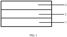
- FIG. 1 is a structural schematic diagram of an organic electroluminescent device of the present invention. Wherein: 1-first electrode layer, 2-light emitting layer, 3-second electrode layer.
- an organic electroluminescent device in the present invention comprises a substrate and light emitting units formed in sequence on the substrate, wherein, each of the light emitting units comprises a first electrode layer 1, a light emitting layer 2 and a second electrode layer 3; the light emitting layer comprises a host material and a dye; the host material is made of materials having both electron transport capability and hole transport capability; at least one material in the host material has a CT excited triplet state energy level T 1 greater than its n- ⁇ excited triplet state energy level S 1 , and T 1 -S 1 ⁇ 0.3eV; or, at least one material in the host material has a CT excited triplet state energy level T 1 greater than its n- ⁇ excited triplet state energy level S 1 , and T 1 -S 1 ⁇ 1eV, with the difference between its n- ⁇ excited second triplet state energy level and its CT excited first singlet state energy level being in the range of -0.1eV to 0.1eV.
- a thermal activating delayed fluorescence material is a material in which there exists charge transfer transition. Both donor group units and receptor group units exist simultaneously in a thermal activating delayed fluorescence material, which gives the thermal activating delayed fluorescence material both electron transport capability and hole transport capability, wherein, the donor group unit is one donor group or a group formed by two or more donor groups being connected together, the receptor group unit is one receptor group or a group formed by two or more receptor groups being connected together.
- the thermal activating delayed fluorescence material has a structure selected from the structural formulas (1-1) to (1-100).
- the host material in the present invention may be an exciplex made from a single thermal activating delayed fluorescence material, or an exciplex made from an electron transport type material and a hole transport type material, or a composition made from a thermal activating delayed fluorescence material (TADF) and a hole transport type material, or a composition made from a thermal activating delayed fluorescence material (TADF) and an electron transport type material.
- TADF thermal activating delayed fluorescence material
- TADF thermal activating delayed fluorescence material
- the electron transport type material is tri-(8-oxyquinoline)-aluminum, 2,9-dimethyl-4,7-diphenyl-1,10-o-phenanthroline, 4,7-diphenyl-1,10-o-phenanthroline, di-(2-methyl-8-quinolyl)-4-phenyl-phenoxide-aluminum(III), 1,3,5-tri-(1-phenyl-1H-benzimidazole-2-yl)-benzene, or 1,3,5-tri-[(3-pyridyl)-3-phenyl]-benzene.
- the hole transport type material is N,N'-di-(1-naphthyl)-N,N'-diphenyl-1,1'-biphenyl-4,4'-diamine, N,N'-diphenyl-N,N'-di-(m-methyl-phenyl)-1,1'-biphenyl-4,4'-diamine, 4,4'-cyclohexyl-di-[N,N-di-(4-methyl-phenyl)]-phenylamine, 4,4'-N,N'-di-carbazole-biphenyl, 4,4',4"-tri-(carbazole-9-yl)-triphenylamine, or 1,3-di-(carbazole-9-yl)-benzene.
- the red dye used in the present invention is selected from the following structural formulas:
- the green dye used in the present invention is selected from the following structural formulas:
- the blue dye used in the present invention is selected from the following structural formulas:
- a device 1 of this embodiment has the following structure:
- the device 1 consists of a substrate, an anode layer, a light emitting layer and a cathode layer, without any hole injection layer, hole transport layer, electron injection layer or electron transport layer.
- the host material of the light emitting layer is made from the thermal activating delayed fluorescence material of the formula (1-24) and the hole transport type material of CBP, at a mass ratio of 1:1.
- the preparation method of the device 1 is as follows: evaporation coating an anode layer (ITO), a light emitting layer and a cathode layer (cathode) in sequence on a substrate by using an open mask, wherein the light emitting layer is prepared by co-evaporation coating of a host material (1-24) : CBP and a dye Ir(piq) 2 (acac), the doping concentration of the dye Ir(piq) 2 (acac) is 5wt%.
- a device 2 of this embodiment has the following structure:
- the host material of the light emitting layer is made from an electron transport type material and the thermal activating delayed fluorescence material of the formula (1-88), at a mass ratio of 1:1.
- the thermal activating delayed fluorescence material serves as a hole transport type material.
- the preparation method of the device 2 comprises the steps of evaporation coating an anode layer (ITO), a light emitting layer and a cathode layer (cathode) in sequence on a substrate by using an open mask, wherein the light emitting layer is prepared by co-evaporation coating of a host material (1-88) : BAlq and a dye Ir(piq) 2 (acac), the doping concentration of the dye Ir(piq) 2 (acac) is 5wt%.
- a host material (1-88) : BAlq and a dye Ir(piq) 2 (acac)
- the doping concentration of the dye Ir(piq) 2 (acac) is 5wt%.
- a device 3 of this embodiment has the following structure:
- the host material of the light emitting layer is an exciplex made from an electron transport type thermal activating delayed fluorescence material and a hole transport type thermal activating delayed fluorescence material), at a mass ratio of 1:1.
- the preparation method of the device 3 is as follows: evaporation coating an anode layer (ITO), a light emitting layer and a cathode layer (cathode) in sequence on a substrate by using an open mask, wherein the light emitting layer is prepared by co-evaporation coating of a host material (1-88) : (1-24) and a dye Ir(piq) 2 (acac), the doping concentration of the dye Ir(piq) 2 (acac) is 5wt%.
- a comparison device 1 of this example has the following structure:
- a comparison device 2 of this example has the following structure:
- a comparison device 3 of this example has the following structure:
- Devices 4-12 of these embodiments have the following structure:
- the preparation method of the devices 4-12 comprises the step of evaporation coating an anode layer (ITO), a light emitting layer and a cathode layer (cathode) in sequence on a substrate by using an open mask, wherein the light emitting layer is prepared by co-evaporation coating of a host material (TADF : hole transport type material) and a fluorescence material.
- ITO anode layer
- cathode cathode
- TADF hole transport type material
- Devices 13-30 of these embodiments have the following structure:
- the preparation method of the devices 13-30 comprises the step of evaporation coating an anode layer (ITO), a light emitting layer and a cathode layer (cathode) in sequence on a substrate by using an open mask, wherein the light emitting layer is prepared by co-evaporation coating of a host material (TADF : electron transport type material) and a fluorescence material.
- ITO anode layer
- cathode cathode
- TADF electron transport type material
- Devices 31-45 of these embodiments have the following structure:
- the preparation method of the devices 31-45 comprises the step of evaporation coating an anode layer (ITO), a light emitting layer and a cathode layer (cathode) in sequence on a substrate by using an open mask, wherein the light emitting layer is prepared by co-evaporation coating of a host material (TADF : hole transport type material) and a phosphorescence material.
- ITO anode layer
- cathode cathode
- TADF hole transport type material
- Devices 46-60 of these embodiments have the following structure:
- the preparation method of the devices 46-60 comprises the step of evaporation coating an anode layer (ITO), a light emitting layer and a cathode layer (cathode) in sequence on a substrate by using an open mask, wherein the light emitting layer is prepared by co-evaporation coating of a host material (TADF : electron transport type material) and a phosphorescence material.
- ITO anode layer
- cathode cathode
- TADF electron transport type material
- Devices 61-74 of these embodiments have the following structure:
- the preparation method of the devices 61-74 comprises the step of evaporation coating an anode layer (ITO), a light emitting layer and a cathode layer (cathode) in sequence on a substrate by using an open mask, wherein the light emitting layer is prepared by co-evaporation coating of a host material TADF and a dye.
- ITO anode layer
- cathode cathode
- Test results of performance of some devices of the above-mentioned Devices 4-74 are listed as follows: Device Brightness (cd/m 2 ) Luminous efficiency (cd/A) External quantum efficiency (%) Service life T 90 (hrs) Device 4 5000 20 17 520 Device 8 5000 17 16 498 Device 10 1000 10 4 163 Device 12 1000 9 3 150 Device 15 1000 6 5 155 Device 18 1000 8 5 164 Device 20 1000 8 5 160 Device 24 5000 20 19 392 Device 26 5000 16 17 511 Device 30 5000 17 17 509 Device 35 5000 60 16 398 Device 40 1000 4 6 89 Device 48 1000 4 5 79 Device 55 1000 6 5 80 Device 62 5000 19 17 355 Device 68 5000 57 15 472 Device 70 1000 5 6 74 Device 72 5000 52 14 394 Device 74 1000 7 13 88
- the synthesis method of the compound of formula (1-85) is as follows: in a nitrogen atmosphere, 1mol potassium tert-butoxide is dissolved in 20mL DML with stirring for 1 hour, then a DML solution containing 1mol carbazole is added dropwise therein, after that the resultant solution is stirred for 1 hour; then, a DMF solution containing 0.2mol 2,3,4,5,6-pentafluorobenzonitrile is added dropwise therein, after that the resultant solution is stirred for 5 hours; then, the reacted liquid is poured into water, and solid is obtained after filtration and separated by using a chromatographic column. Thereby the compound of formula (1-85) is produced, with a yield rate of 90%.
- the reactant carbazole is replaced by tert-butyl carbazole, and a synthesis process similar to that of Embodiment 75 is carried out to produce the compound of formula (1-86), with a yield rate of 91%.
- the reactant carbazole is replaced by phenyl carbazole, and a synthesis process similar to that of Embodiment 75 is carried out to produce the compound of formula (1-87), with a yield rate of 91%.
- the synthesis method of the compound of formula (1-88) is as follows: in a nitrogen atmosphere, 1mol potassium tert-butoxide is dissolved in 20mL DML with stirring for 1 hour, then a DML solution containing 1mol carbazole is added dropwise therein, after that the resultant solution is stirred for 1 hour; then, a DMF solution containing 0.25mol 2,3,5,6-tetrafluorobenzonitrile is added dropwise therein, after that the resultant solution is stirred for 5 hours; then, the reacted liquid is poured into water, and solid is obtained after filtration and separated by using a chromatographic column. Thereby the compound of formula (1-88) is produced, with a yield rate of 90%.
- the reactant carbazole is replaced by tert-butyl carbazole, and a synthesis process similar to that of Embodiment 78 is carried out to produce the compound of formula (1-89), with a yield rate of 91%.
- the reactant carbazole is replaced by methyl carbazole, and a synthesis process similar to that of Embodiment 78 is carried out to produce the compound of formula (1-90), with a yield rate of 91%.
- the reactant carbazole is replaced by phenyl carbazole, and a synthesis process similar to that of Embodiment 78 is carried out to produce the compound of formula (1-91), with a yield rate of 91%.
- the reactant carbazole is replaced by methoxyl carbazole, and a synthesis process similar to that of Embodiment 78 is carried out to produce the compound of formula (1-92), with a yield rate of 91%.
- the synthesis method of the compound of formula (1-93) is as follows: in a nitrogen atmosphere, 1mol potassium tert-butoxide is dissolved in 20mL DML with stirring for 1 hour, then a DML solution containing 1mol methoxyl carbazole is added dropwise therein, after that the resultant solution is stirred for 1 hour; then, a DMF solution containing 0.33mol 2,4,6-trifluorobenzonitrile is added dropwise therein, after that the resultant solution is stirred for 5 hours; then, the reacted liquid is poured into water, and solid is obtained after filtration and separated by using a chromatographic column. Thereby the compound of formula (1-93) is produced, with a yield rate of 90%.
- the reactant carbazole is replaced by tert-butyl carbazole, and a synthesis process similar to that of Embodiment 83 is carried out to produce the compound of formula (1-94), with a yield rate of 91%.
- the reactant carbazole is replaced by phenoxazine, and a synthesis process similar to that of Embodiment 83 is carried out to produce the compound of formula (1-95), with a yield rate of 91%.
- the reactant carbazole is replaced by phenothiazine, and a synthesis process similar to that of Embodiment 83 is carried out to produce the compound of formula (1-96), with a yield rate of 91%.
- the reactant carbazole is replaced by acridine, and a synthesis process similar to that of Embodiment 83 is carried out to produce the compound of formula (1-97), with a yield rate of 91%.
- the reactant carbazole is replaced by phenazine, and a synthesis process similar to that of Embodiment 83 is carried out to produce the compound of formula (1-98), with a yield rate of 91%.
Landscapes
- Chemical & Material Sciences (AREA)
- Organic Chemistry (AREA)
- Engineering & Computer Science (AREA)
- Physics & Mathematics (AREA)
- Materials Engineering (AREA)
- Spectroscopy & Molecular Physics (AREA)
- Optics & Photonics (AREA)
- Inorganic Chemistry (AREA)
- Manufacturing & Machinery (AREA)
- Electroluminescent Light Sources (AREA)
Abstract
Description
- The present invention relates to the technical field of organic electroluminescent devices, and in particular relates to an organic electroluminescent device with a single-layered organic layer.
- An organic electroluminescent device (OLED) usually includes a plurality of pixels, and each pixel is composed of several sub-pixels. Currently, one widely used solution in small and medium sized devices is forming a pixel with three sub-pixels of red, green and blue. Each kind of sub-pixel comprises a hole transport layer, a light emitting layer, an electron transport layer, and a hole/exciton blocking layer arranged between the light emitting layer and the electron transport layer, wherein the light emitting layer comprises a blue light emitting layer, a green light emitting layer or a red light emitting layer. Besides, a green optical compensation layer and a red light emitting layer might be required to be arranged between the hole transport layer and an electrode layer, which further adds to the processing steps.
- In order to solve the above-mentioned problem, it is explored to use a device configuration with a single-layered light emitting layer. However, in conventional OLED devices with single-layered light emitting layer, because most organic materials have imbalanced carrier injection and different carriers have hugely different transporting speed, the light emitting area easily shifts to the side of the injection electrode with a lower migration rate. In the condition of a metal electrode, this may easily cause light-emitting to be quenched by the electrode, which negatively affects the efficiency and service life of the device.
- Thus, the present invention is intended to solve the technical problem that the organic electroluminescent devices in prior arts with the existing configuration of single-layered structure have a short service life because of exciton quenching, by providing an organic electroluminescent device that can sufficiently utilize the triplet state energy in the host material and the dye to increase the luminous efficiency and prolong the service life of the device.
- The present invention also provides a preparation method of the above-mentioned organic electroluminescent device.
- In order to solve the above-mentioned technical problem, the present invention adopts the following technical scheme:
- An organic electroluminescent device comprises a substrate and light emitting units formed in sequence on the substrate, and each of the light emitting units comprises a first electrode layer, a light emitting layer and a second electrode layer, the light emitting layer comprises a host material and a dye, the host material is made of materials having both electron transport capability and hole transport capability; at least one material in the host material has a CT excited triplet state energy level T1 greater than its n-π excited triplet state energy level S1, and T1-S1 ≤ 0.3eV; or, at least one material in the host material has a CT excited triplet state energy level T1 greater than its n-π excited triplet state energy level S1, and T1-S1 ≥ 1eV, with the difference between its n-π excited second triplet state energy level and its CT excited first singlet state energy level being in the range of -0.1eV to 0.1eV.
- Preferably, the host material is an exciplex, and the exciplex is a thermal activating delayed fluorescence material.
- Alternatively, the host material is an exciplex made from an electron transport type material and a hole transport type material at a mass ratio of 1:9 to 9:1. Wherein, the electron transport type material and/or the hole transport type material has T1-S1 ≤ 0.3eV; or, the electron transport type material and/or the hole transport type material has T1-S1 ≥ 1eV, with the difference between the n-π excited second triplet state energy level and the CT excited first singlet state energy level of the host material being in the range of -0.1eV to 0.1eV.
- Alternatively, the host material is composed of a thermal activating delayed fluorescence material and a hole transport type material at a mass ratio of 1:9 to 9:1. Wherein, the thermal activating delayed fluorescence material and/or the hole transport type material has T1-S1 ≤ 0.3eV; or, the thermal activating delayed fluorescence material and/or the hole transport type material has T1-S1 ≥ 1eV, with the difference between the n-π excited second triplet state energy level and the CT excited first singlet state energy level of the host material being in the range of -0.1eV to 0.1eV.
- Alternatively, the host material is composed of a thermal activating delayed fluorescence material and an electron transport type material at a mass ratio of 1:9 to 9:1. Wherein, the thermal activating delayed fluorescence material and/or the electron transport type material has T1-S1 ≤ 0.3eV; or, the thermal activating delayed fluorescence material and/or the electron transport type material has T1-S1 ≥ 1eV, with the difference between the n-π excited second triplet state energy level and the CT excited first singlet state energy level of the host material being in the range of -0.1eV to 0.1eV.
- The dye is made of a fluorescence material and/or a phosphorescence material, the fluorescence material has a doping concentration of 0.5-10wt%, the phosphorescence material has a doping concentration of 0.5-20wt%.
- The light emitting layer has a thickness of 50nm-150nm.
- The electron transport type material is tri-(8-oxyquinoline)-aluminum, 2,9-dimethyl-4,7-diphenyl-1,10-o-phenanthroline, 4,7-diphenyl-1,10-o-phenanthroline, di-(2-methyl-8-quinolyl)-4-phenyl-phenoxide-aluminum(III), 1,3,5-tri-(1-phenyl-1H-benzimidazole-2-yl)-benzene, or 1,3,5-tri-[(3-pyridyl)-3-phenyl]-benzene.
- The hole transport type material is N,N'-di-(1-naphthyl)-N,N'-diphenyl-1,1'-biphenyl-4,4'-diamine, N,N'-diphenyl-N,N'-di-(m-methyl-phenyl)-1,1'-biphenyl-4,4'-diamine, 4,4'-cyclohexyl-di-[N,N-di-(4-methyl-phenyl)]-phenylamine, 4,4'-N,N'-di-carbazole-biphenyl, 4,4',4"-tri-(carbazole-9-yl)-triphenylamine, or 1,3-di-(carbazole-9-yl)-benzene.
- The thermal activating delayed fluorescence (TADF) material has a structure selected from the following structural formulas (1-1) to (1-100):


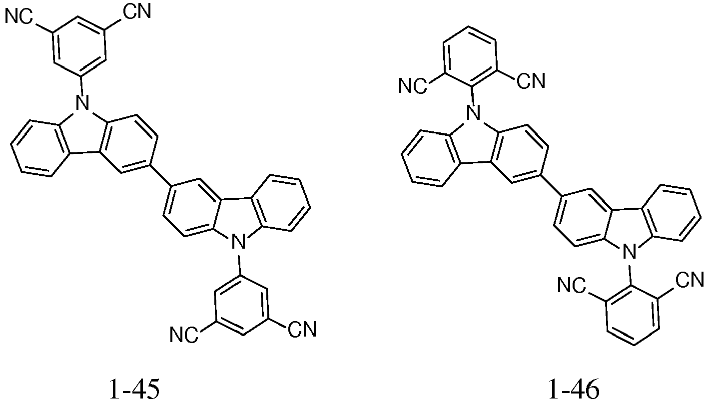


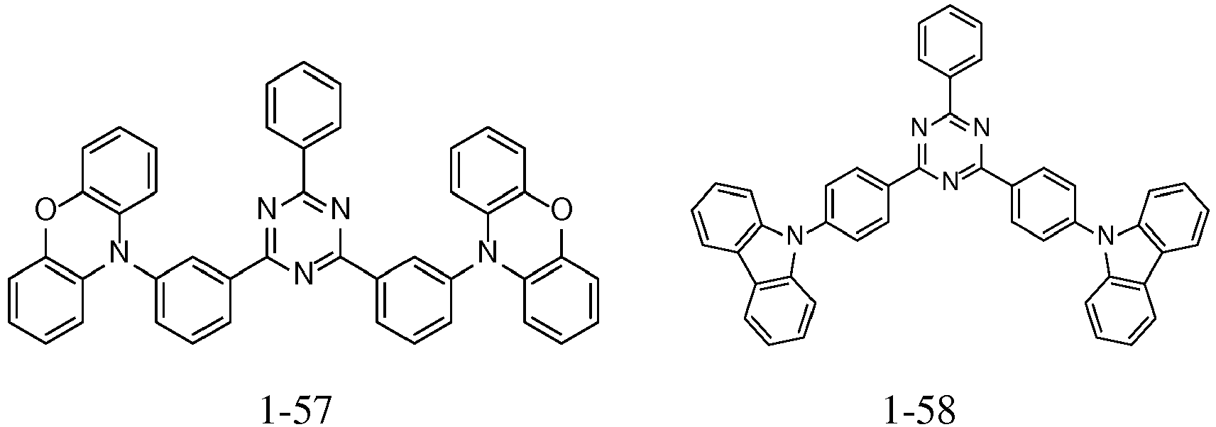


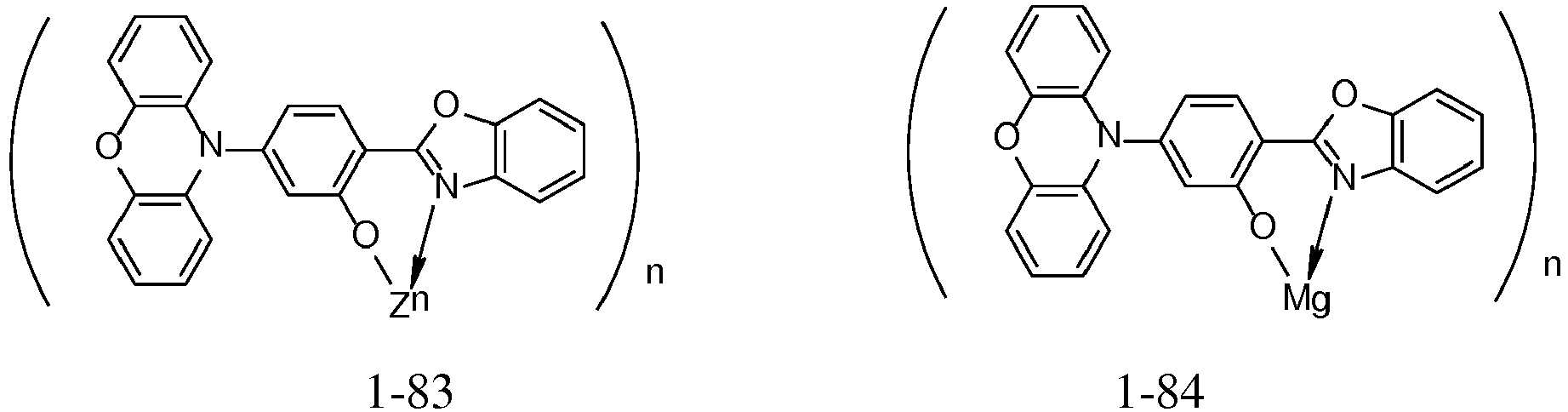


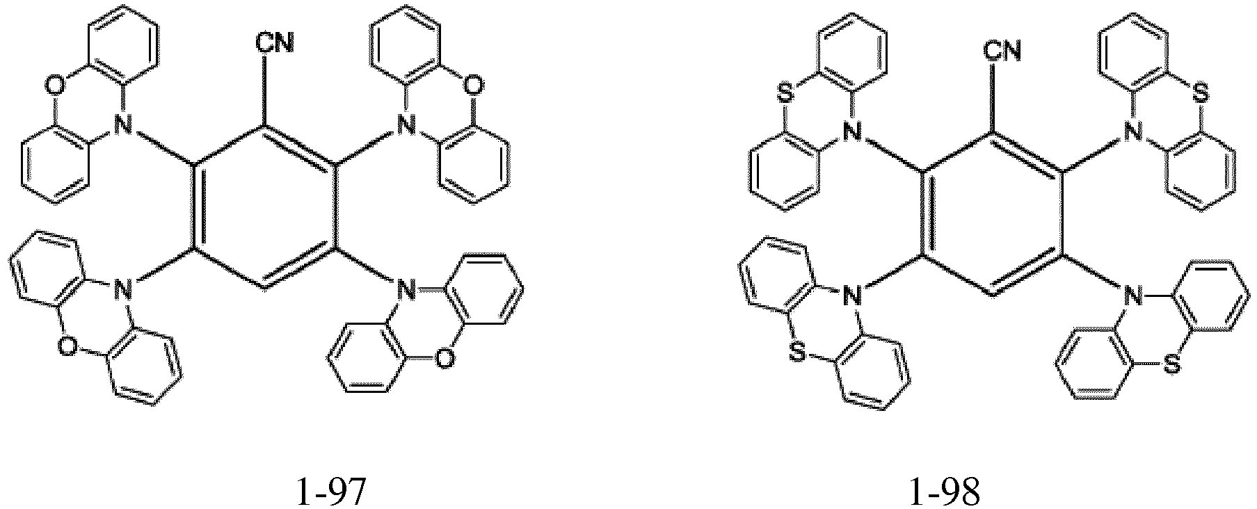

- A preparation method of the aforementioned organic electroluminescent device comprises the following steps:
- evaporation coating a first electrode layer, a light emitting layer and a second electrode layer in sequence on a substrate by using an open mask;
- wherein, the light emitting layer is prepared by co-evaporation coating of a host material and a dye.
- As compared to prior arts, the above-mentioned technical scheme of the present invention has the following advantages:
- (1) The present invention aims to providing a single-layered device configuration, wherein the organic electroluminescent device only needs to consist of a first electrode layer, a light emitting layer and a second electrode layer, and the light emitting layer is prepared by co-evaporation coating of only a host material and a dye, without the necessity to prepare other organic layers such as a hole transport layer, a hole blocking layer, an electron transport layer or an electron blocking layer, so that the structure of the device is greatly simplified, the preparation process is shortened, and the production cost is reduced.
- (2) In the present invention, the host material has T1-S1 ≤ 0.3eV, such material has small difference between its singlet state energy level and its triplet state energy level, in particular, the host material may be a thermal activating delayed fluorescence material (TADF), or an exciplex made from an electron transport type material and a hole transport type material, or a composition made from a thermal activating delayed fluorescence material (TADF) and a hole transport type material, or a composition made from a thermal activating delayed fluorescence material (TADF) and an electron transport type material, these three types of compositions have donor groups and receptor groups, and therefore have capabilities to transport both holes and electrons. Meanwhile, the device configuration adopted by the present invention can sufficiently utilize the triplet state energy in the host material and the dye, because the difference between the singlet state energy level and the triplet state energy level is small, which is beneficial for injection of electrons and holes, so that the problem of low efficiency and short service life caused by exciton quenching can be solved. Therefore, the luminous efficiency can be increased and the service life of the device can be prolonged.
- In order to make the content of the present invention more easy to be understood clearly, hereinafter, the present invention is further described in detail according to specific embodiments of the present invention with reference to the accompanying drawings, wherein,
-
FIG. 1 is a structural schematic diagram of an organic electroluminescent device of the present invention.
Wherein: 1-first electrode layer, 2-light emitting layer, 3-second electrode layer. - The present invention is further described hereinafter by illustrating specific embodiments.
- The present invention can be implemented in many different forms, and should not be interpreted to be limited to the embodiments described herein. On the contrary, by providing these embodiments, the present disclosure is made complete and thorough, and the inventive concept of the present invention is sufficiently conveyed to those skilled in the art, wherein the present invention is defined by the Claims. In the accompanying drawings, for the sake of clarity, dimensions and relative sizes of layers and areas might be exaggerated. It should be understood that, when one element such as a layer, an area or a substrate plate is described as "formed on" or "configured on" another element, this one element may be configured directly upon that another element, or there may exist intermediate element(s). On the contrary, when one element is described as "directly formed upon" or "directly configured upon" another element, there exist no intermediate element.
- As shown in
FIG. 1 , an organic electroluminescent device in the present invention comprises a substrate and light emitting units formed in sequence on the substrate, wherein, each of the light emitting units comprises afirst electrode layer 1, alight emitting layer 2 and asecond electrode layer 3; the light emitting layer comprises a host material and a dye; the host material is made of materials having both electron transport capability and hole transport capability; at least one material in the host material has a CT excited triplet state energy level T1 greater than its n-π excited triplet state energy level S1, and T1-S1 ≤ 0.3eV; or, at least one material in the host material has a CT excited triplet state energy level T1 greater than its n-π excited triplet state energy level S1, and T1-S1 ≥ 1eV, with the difference between its n-π excited second triplet state energy level and its CT excited first singlet state energy level being in the range of -0.1eV to 0.1eV. - A thermal activating delayed fluorescence material is a material in which there exists charge transfer transition. Both donor group units and receptor group units exist simultaneously in a thermal activating delayed fluorescence material, which gives the thermal activating delayed fluorescence material both electron transport capability and hole transport capability, wherein, the donor group unit is one donor group or a group formed by two or more donor groups being connected together, the receptor group unit is one receptor group or a group formed by two or more receptor groups being connected together. In particular, the thermal activating delayed fluorescence material has a structure selected from the structural formulas (1-1) to (1-100).
- The host material in the present invention may be an exciplex made from a single thermal activating delayed fluorescence material, or an exciplex made from an electron transport type material and a hole transport type material, or a composition made from a thermal activating delayed fluorescence material (TADF) and a hole transport type material, or a composition made from a thermal activating delayed fluorescence material (TADF) and an electron transport type material.
- The electron transport type material is tri-(8-oxyquinoline)-aluminum, 2,9-dimethyl-4,7-diphenyl-1,10-o-phenanthroline, 4,7-diphenyl-1,10-o-phenanthroline, di-(2-methyl-8-quinolyl)-4-phenyl-phenoxide-aluminum(III), 1,3,5-tri-(1-phenyl-1H-benzimidazole-2-yl)-benzene, or 1,3,5-tri-[(3-pyridyl)-3-phenyl]-benzene.
Abbreviation Full name Structural formula Alq3 tri-(8-oxyquinoline)- aluminum 
BCP 2,9-dimethyl-4,7-diphenyl-1,10-o-phenanthroline 
Bphen 4,7-diphenyl-1,10-o-phenanthroline 
BAlq di-(2-methyl-8-quinolyl)-4-phenyl-phenoxide-aluminum(III) 
TPBi 1,3,5-tri-(1-phenyl-1H-benzimidazole-2-yl) - benzene 
TmPyPB 1,3,5-tri-[(3-pyridyl)-3-phenyl]-benzene 
- The hole transport type material is N,N'-di-(1-naphthyl)-N,N'-diphenyl-1,1'-biphenyl-4,4'-diamine, N,N'-diphenyl-N,N'-di-(m-methyl-phenyl)-1,1'-biphenyl-4,4'-diamine, 4,4'-cyclohexyl-di-[N,N-di-(4-methyl-phenyl)]-phenylamine, 4,4'-N,N'-di-carbazole-biphenyl, 4,4',4"-tri-(carbazole-9-yl)-triphenylamine, or 1,3-di-(carbazole-9-yl)-benzene.
Abbreviation Full name Structural formula NPB N,N'-di-(1-naphthyl)-N,N'-diphenyl-1,1'-biphenyl-4,4'-diamine 
TPD N,N'-diphenyl-N,N'-di-(m-methyl-phenyl)-1,1'-biphenyl-4,4'-diamine 
TAPC 4,4'-cyclohexyl-di-[N,N-di-(4-methyl-phenyl)]-phenylamine 
CBP 4,4'-N,N'-di-carbazole-biphenyl 
TCTA 4,4',4"-tri-(carbazole-9-yl)- triphenylamine 
mCP 1,3-di-(carbazole-9-yl)-benzene 
- The red dye used in the present invention is selected from the following structural formulas:


- The green dye used in the present invention is selected from the following structural formulas:


- The blue dye used in the present invention is selected from the following structural formulas:


- A
device 1 of this embodiment has the following structure: - glass / ITO / (1-24) : CBP: Ir(piq)2(acac)(5%) / cathode
- The
device 1 consists of a substrate, an anode layer, a light emitting layer and a cathode layer, without any hole injection layer, hole transport layer, electron injection layer or electron transport layer. The host material of the light emitting layer is made from the thermal activating delayed fluorescence material of the formula (1-24) and the hole transport type material of CBP, at a mass ratio of 1:1. - The preparation method of the
device 1 is as follows: evaporation coating an anode layer (ITO), a light emitting layer and a cathode layer (cathode) in sequence on a substrate by using an open mask, wherein the light emitting layer is prepared by co-evaporation coating of a host material (1-24) : CBP and a dye Ir(piq)2(acac), the doping concentration of the dye Ir(piq)2(acac) is 5wt%. - A
device 2 of this embodiment has the following structure: - glass / ITO / (1-88) : BAlq : Ir(piq)2(acac)(5%) / cathode
- In the
device 2, the host material of the light emitting layer is made from an electron transport type material and the thermal activating delayed fluorescence material of the formula (1-88), at a mass ratio of 1:1. Herein, the thermal activating delayed fluorescence material serves as a hole transport type material. - The preparation method of the
device 2 comprises the steps of evaporation coating an anode layer (ITO), a light emitting layer and a cathode layer (cathode) in sequence on a substrate by using an open mask, wherein the light emitting layer is prepared by co-evaporation coating of a host material (1-88) : BAlq and a dye Ir(piq)2(acac), the doping concentration of the dye Ir(piq)2(acac) is 5wt%. - A
device 3 of this embodiment has the following structure: - glass / ITO / (1-88) : (1-24) : Ir(piq)2(acac)(5%) / cathode
- In the
device 3, the host material of the light emitting layer is an exciplex made from an electron transport type thermal activating delayed fluorescence material and a hole transport type thermal activating delayed fluorescence material), at a mass ratio of 1:1. - The preparation method of the
device 3 is as follows: evaporation coating an anode layer (ITO), a light emitting layer and a cathode layer (cathode) in sequence on a substrate by using an open mask, wherein the light emitting layer is prepared by co-evaporation coating of a host material (1-88) : (1-24) and a dye Ir(piq)2(acac), the doping concentration of the dye Ir(piq)2(acac) is 5wt%. - A
comparison device 1 of this example has the following structure: - glass / ITO / HIL / HTL / CBP: Ir(piq)2(acac)(5%) / HBL / ETL / cathode
- A
comparison device 2 of this example has the following structure: - glass / ITO / HIL / HTL / BAlq : Ir(piq)2(acac)(20%) / HBL / ETL / cathode
- A
comparison device 3 of this example has the following structure: - glass / ITO / HIL / HTL / CBP : BAlq : Ir(piq)2(acac)(5%) / HBL / ETL / cathode
- Devices 4-12 of these embodiments have the following structure:
- glass / ITO / TADF : hole transport type material: fluorescence material / cathode
- Wherein, the respective materials and mass ratios of the TADF, the hole transport type material and the fluorescence material are listed in Table 2.
- Wherein the doping concentration of the fluorescence material refers to the ratio that the fluorescence material accounts for in the total mass of the light emitting layer, that is, the fluorescence material doping concentration = the fluorescence material mass / (the fluorescence material mass + the TADF mass + the hole transport type material mass) *100%.
- The preparation method of the devices 4-12 comprises the step of evaporation coating an anode layer (ITO), a light emitting layer and a cathode layer (cathode) in sequence on a substrate by using an open mask, wherein the light emitting layer is prepared by co-evaporation coating of a host material (TADF : hole transport type material) and a fluorescence material.
Table 2 TADF Hole transport type material Mass ratio fluorescence material doping concentration of the fluorescence material Device 4 Formula (1-1) NPB 1:9 DCJT 15wt% Device 5 Formula (1-2) TCTA 2:8 BCzVBi 15wt% Device 6 Formula (1-3) CBP 3:7 DPAVBi 5wt% Device 7 Formula (1-4) mCP 4:5 BCzVBi 5wt% Device 8 Formula (1-5) TPD 5:4 DCJT 5wt% Device 9 Formula (1-6) TAPC 6:3 DCJT 5wt% Device 10 Formula (1-11) CBP 7:2 BCzVBi 5wt% Device 11 Formula (1-15) mCP 8:1 DPAVBi 5wt% Device 12 Formula (1-20) mCP 9:1 BCzVBi 5wt% - Devices 13-30 of these embodiments have the following structure:
- glass / ITO / TADF : electron transport type material: fluorescence material / cathode
- Wherein, the respective materials and mass ratios of the TADF, the electron transport type material and the fluorescence material are listed in Table 3.
- Wherein the doping concentration of the fluorescence material refers to the ratio that the fluorescence material accounts for in the total mass of the light emitting layer, that is, the fluorescence material doping concentration = the fluorescence material mass / (the fluorescence material mass + the TADF mass + the electron transport type material mass) *100%.
- The preparation method of the devices 13-30 comprises the step of evaporation coating an anode layer (ITO), a light emitting layer and a cathode layer (cathode) in sequence on a substrate by using an open mask, wherein the light emitting layer is prepared by co-evaporation coating of a host material (TADF : electron transport type material) and a fluorescence material.
Table 3 TADF Electron transport type material Mass ratio fluorescence material doping concentration of the fluorescence material Device 13 Formula (1-21) TmPyPB 1:9 DCJT 5wt% Device 14 Formula (1-22) TPBi 2:8 BCzVBi 5wt% Device 15 Formula (1-23) BCP 3:7 DPAVBi 5wt% Device 16 Formula (1-24) Bphen 4:5 BCzVBi 5wt% Device 17 Formula (1-25) BCP 5:4 DCJT 5wt% Device 18 Formula (1-26) Alq3 6:3 BCzVBi 5wt% Device 19 Formula (1-31) Bphen 7:2 DPAVBi 5wt% Device 20 Formula (1-35) BCP 8:1 BCzVBi 5wt% Device 21 Formula (1-40) BAlq 9:1 DCJT 5wt% Device 22 Formula (1-45) Alq3 1:9 DCM 5wt% Device 23 Formula (1-48) BAlq 2:8 DMQA 15wt% Device 24 Formula (1-50) TPBi 3:7 TMDBQA 15wt% Device 25 Formula (1-51) Bphen 4:5 DPAVB 5wt% Device 26 Formula (1-55) Bphen 5:4 Rubrene 5wt% Device 27 Formula (1-60) TPBi 6:3 DCJTB 5wt% Device 28 Formula (1-65) BAlq 7:2 DBQA 15wt% Device 29 Formula (1-78) TmPyPB 8:1 DCM2 5wt% Device 30 Formula (1-86) Bphen 9:1 Rubrene 5wt% - Devices 31-45 of these embodiments have the following structure:
- glass / ITO / TADF : hole transport type material: phosphorescence material / cathode
- Wherein, the respective materials and mass ratios of the TADF, the hole transport type material and the phosphorescence material are listed in Table 4.
- Wherein the doping concentration of the phosphorescence material refers to the ratio that the phosphorescence material accounts for in the total mass of the light emitting layer, that is, the phosphorescence material doping concentration = the phosphorescence material mass / (the phosphorescence material mass + the TADF mass + the hole transport type material mass) *100%.
- The preparation method of the devices 31-45 comprises the step of evaporation coating an anode layer (ITO), a light emitting layer and a cathode layer (cathode) in sequence on a substrate by using an open mask, wherein the light emitting layer is prepared by co-evaporation coating of a host material (TADF : hole transport type material) and a phosphorescence material.
Table 4 TADF Hole transport type material Mass ratio phosphorescence material doping concentration of the phosphorescence material Device 31 Formula (1-32) NPB 1:9 Ir(ppy)3 30wt% Device 32 Formula (1-33) TCTA 2:8 Ir(ppy)2(acac) 15wt% Device 33 Formula (1-34) CBP 3:7 FIrPic 5wt% Device 34 Formula (1-56) mCP 4:5 Ir(2-phq)2(acac) 15wt% Device 35 Formula (1-36) TPD 5:4 Ir(ppy)2(acac) 30wt% Device 36 Formula (1-37) TAPC 6:3 Ir(btpy)3 20wt% Device 37 Formula (1-38) CBP 7:2 Be(pp)2 5wt% Device 38 Formula (1-39) mCP 8:1 Ir(piq)2(acac) 15wt% Device 39 Formula (1-41) mCP 9:1 Ir(ppy)3 30wt% Device 40 Formula (1-42) NPB 1:9 FIrPic 5wt% Device 41 Formula (1-43) CBP 2:8 Ir(piq)2(acac) 15wt% Device 42 Formula (1-44) TAPC 3:7 Ir(ppy)2(acac) 15wt% Device 43 Formula (1-46) NPB 4:5 FIr6 10wt% Device 44 Formula (1-47) TCTA 5:4 Ir(piq)2(acac) 30wt% Device 45 Formula (1-49) CBP 6:3 Be(pp)2 5wt% - Devices 46-60 of these embodiments have the following structure:
- glass / ITO / TADF : electron transport type material: phosphorescence material / cathode
- Wherein, the respective materials and mass ratios of the TADF, the electron transport type material and the phosphorescence material are listed in Table 5.
- Wherein the doping concentration of the phosphorescence material refers to the ratio that the phosphorescence material accounts for in the total mass of the light emitting layer, that is, the phosphorescence material doping concentration = the phosphorescence material mass / (the phosphorescence material mass + the TADF mass + the electron transport type material mass) *100%.
- The preparation method of the devices 46-60 comprises the step of evaporation coating an anode layer (ITO), a light emitting layer and a cathode layer (cathode) in sequence on a substrate by using an open mask, wherein the light emitting layer is prepared by co-evaporation coating of a host material (TADF : electron transport type material) and a phosphorescence material.
Table 5 TADF Electron transport type material Mass ratio phosphorescence material doping concentration of the phosphorescence material Device 46 Formula (1-52) BAlq 1:9 Ir(ppy)3 30wt% Device 47 Formula (1-53) TPBi 2:8 Ir(ppy)2(acac) 15wt% Device 48 Formula (1-54) Bphen 3:7 FIrPic 5wt% Device 49 Formula (1-57) Bphen 4:5 Ir(2-phq)2(acac) 15wt% Device 50 Formula (1-58) Alq3 5:4 Ir(ppy)2(acac) 30wt% Device 51 Formula (1-59) Alq3 6:3 Ir(btpy)3 20wt% Device 52 Formula (1-72) Bphen 7:2 Be(pp)2 5wt% Device 53 Formula (1-76) BCP 8:1 Ir(piq)2(acac) 15wt% Device 54 Formula (1-80) TmPyPB 9:1 Ir(ppy)3 30wt% Device 55 Formula (1-82) TPBi 1:9 FIrPic 5wt% Device 56 Formula (1-83) BAlq 2:8 Ir(piq)2(acac) 15wt% Device 57 Formula (1-85) TPBi 3:7 Ir(ppy)2(acac) 15wt% Device 58 Formula (1-63) BCP 4:5 FIr6 10wt% Device 59 Formula (1-68) Bphen 5:4 Ir(piq)2(acac) 30wt% Device 60 Formula (1-66) BCP 6:3 Be(pp)2 5wt% - Devices 61-74 of these embodiments have the following structure:
- glass / ITO / TADF : dye / cathode
- Wherein, the materials and mass ratios of the dye as in the (TADF : dye) are listed in Table 6.
- Wherein the dye is a fluorescence material and/or a phosphorescence material, the doping concentration of the dye refers to the ratio that the dye accounts for in the total mass of the light emitting layer, that is, the dye doping concentration = the dye mass / (the dye mass + the TADF mass) *100%.
- The preparation method of the devices 61-74 comprises the step of evaporation coating an anode layer (ITO), a light emitting layer and a cathode layer (cathode) in sequence on a substrate by using an open mask, wherein the light emitting layer is prepared by co-evaporation coating of a host material TADF and a dye.
Table 6 TADF Dye Dye name dye doping concentration Device 61 Formula (1-87) fluorescence TMDBQA 10wt% Device 62 Formula (1-88) fluorescence DMQA 5wt% Device 63 Formula (1-89) fluorescence DPAVBi 5wt% Device 64 Formula (1-90) fluorescence BCzVBi 5wt% Device 65 Formula (1-91) fluorescence DCJT 5wt% Device 66 Formula (1-92) fluorescence DCJTB 5wt% Device 67 Formula (1-93) fluorescence Rubrene 5wt% Device 68 Formula (1-94) phosphorescence Ir(ppy)3 30wt% Device 69 Formula (1-95) phosphorescence Ir(ppy)2(acac) 15wt% Device 70 Formula (1-96) phosphorescence FIrPic 5wt% Device 71 Formula (1-97) phosphorescence Ir(2-phq)2(acac) 15wt% Device 72 Formula (1-98) phosphorescence Ir(ppy)2 (acac) 30wt% Device 73 Formula (1-99) phosphorescence Ir(btpy)3 20wt% Device 74 Formula (1-100) phosphorescence Be(pp)2 5wt% - Test results of performance of some devices of the above-mentioned Devices 4-74 are listed as follows:
Device Brightness (cd/m2) Luminous efficiency (cd/A) External quantum efficiency (%) Service life T90 (hrs) Device 4 5000 20 17 520 Device 8 5000 17 16 498 Device 10 1000 10 4 163 Device 12 1000 9 3 150 Device 15 1000 6 5 155 Device 18 1000 8 5 164 Device 20 1000 8 5 160 Device 24 5000 20 19 392 Device 26 5000 16 17 511 Device 30 5000 17 17 509 Device 35 5000 60 16 398 Device 40 1000 4 6 89 Device 48 1000 4 5 79 Device 55 1000 6 5 80 Device 62 5000 19 17 355 Device 68 5000 57 15 472 Device 70 1000 5 6 74 Device 72 5000 52 14 394 Device 74 1000 7 13 88 - Embodiments of synthesis of the compound of formula (1-85) to (1-98):
- The synthesis method of the compound of formula (1-85) is as follows: in a nitrogen atmosphere, 1mol potassium tert-butoxide is dissolved in 20mL DML with stirring for 1 hour, then a DML solution containing 1mol carbazole is added dropwise therein, after that the resultant solution is stirred for 1 hour; then, a DMF solution containing 0.2
mol - Mass spectrum: 929.
- Element analysis: C: 86.60, H: 4.35, N: 9.05.
- In the synthesis method of the compound of formula (1-86), the reactant carbazole is replaced by tert-butyl carbazole, and a synthesis process similar to that of Embodiment 75 is carried out to produce the compound of formula (1-86), with a yield rate of 91%.
- Mass spectrum: 1490.
- Element analysis: C: 86.20, H: 8.16, N: 5.64.
- In the synthesis method of the compound of formula (1-87), the reactant carbazole is replaced by phenyl carbazole, and a synthesis process similar to that of Embodiment 75 is carried out to produce the compound of formula (1-87), with a yield rate of 91%.
- Mass spectrum: 1689.
- Element analysis: C: 90.20, H: 4.83, N: 4.97.
- The synthesis method of the compound of formula (1-88) is as follows: in a nitrogen atmosphere, 1mol potassium tert-butoxide is dissolved in 20mL DML with stirring for 1 hour, then a DML solution containing 1mol carbazole is added dropwise therein, after that the resultant solution is stirred for 1 hour; then, a DMF solution containing 0.25
mol - Mass spectrum: 763.
- Element analysis: C: 86.47, H: 4.36, N: 9.17.
- In the synthesis method of the compound of formula (1-89), the reactant carbazole is replaced by tert-butyl carbazole, and a synthesis process similar to that of Embodiment 78 is carried out to produce the compound of formula (1-89), with a yield rate of 91%.
- Mass spectrum: 1212.
- Element analysis: C: 86.15, H: 8.07, N: 5.77.
- In the synthesis method of the compound of formula (1-90), the reactant carbazole is replaced by methyl carbazole, and a synthesis process similar to that of Embodiment 78 is carried out to produce the compound of formula (1-90), with a yield rate of 91%.
- Mass spectrum: 876.
- Element analysis: C: 86.36, H: 5.65, N: 7.99.
- In the synthesis method of the compound of formula (1-91), the reactant carbazole is replaced by phenyl carbazole, and a synthesis process similar to that of Embodiment 78 is carried out to produce the compound of formula (1-91), with a yield rate of 91%.
- Mass spectrum: 1372.
- Element analysis: C: 90.10, H: 4.79, N: 5.10.
- In the synthesis method of the compound of formula (1-92), the reactant carbazole is replaced by methoxyl carbazole, and a synthesis process similar to that of Embodiment 78 is carried out to produce the compound of formula (1-92), with a yield rate of 91%.
- Mass spectrum: 1004.
- Element analysis: C: 75.35, H: 4.93, N: 6.97.
- The synthesis method of the compound of formula (1-93) is as follows: in a nitrogen atmosphere, 1mol potassium tert-butoxide is dissolved in 20mL DML with stirring for 1 hour, then a DML solution containing 1mol methoxyl carbazole is added dropwise therein, after that the resultant solution is stirred for 1 hour; then, a DMF solution containing 0.33
mol 2,4,6-trifluorobenzonitrile is added dropwise therein, after that the resultant solution is stirred for 5 hours; then, the reacted liquid is poured into water, and solid is obtained after filtration and separated by using a chromatographic column. Thereby the compound of formula (1-93) is produced, with a yield rate of 90%. - Mass spectrum: 778.
- Element analysis: C: 75.55, H: 4.93, N: 7.19.
- In the synthesis method of the compound of formula (1-94), the reactant carbazole is replaced by tert-butyl carbazole, and a synthesis process similar to that of Embodiment 83 is carried out to produce the compound of formula (1-94), with a yield rate of 91%.
- Mass spectrum: 935.
- Element analysis: C: 86.00, H: 7.81, N: 5.99.
- In the synthesis method of the compound of formula (1-95), the reactant carbazole is replaced by phenoxazine, and a synthesis process similar to that of Embodiment 83 is carried out to produce the compound of formula (1-95), with a yield rate of 91%.
- Mass spectrum: 829.
- Element analysis: C: 79.79, H: 4.00, N: 8.48.
- In the synthesis method of the compound of formula (1-96), the reactant carbazole is replaced by phenothiazine, and a synthesis process similar to that of Embodiment 83 is carried out to produce the compound of formula (1-96), with a yield rate of 91%.
- Mass spectrum: 892.
- Element analysis: C: 74.05, H: 3.70, N: 7.88.
- In the synthesis method of the compound of formula (1-97), the reactant carbazole is replaced by acridine, and a synthesis process similar to that of Embodiment 83 is carried out to produce the compound of formula (1-97), with a yield rate of 91%.
- Mass spectrum: 932.
- Element analysis: C: 86.32, H: 6.15, N: 7.52.
- In the synthesis method of the compound of formula (1-98), the reactant carbazole is replaced by phenazine, and a synthesis process similar to that of Embodiment 83 is carried out to produce the compound of formula (1-98), with a yield rate of 91%.
- Mass spectrum: 880.
- Element analysis: C: 80.50, H: 5.17, N: 14.32.
- Apparently, the aforementioned embodiments are merely examples illustrated for clearly describing the present invention, rather than limiting the implementation ways thereof. For those skilled in the art, various changes and modifications in other different forms can be made on the basis of the aforementioned description. It is unnecessary and impossible to exhaustively list all the implementation ways herein. However, any obvious changes or modifications derived from the aforementioned description are intended to be embraced within the protection scope of the present invention.
| Device | Brightness (cd/m2) | Luminous efficiency (cd/A) | External quantum efficiency (%) | Service life T90 (hrs) |
| | 5000 | 22 | 24 | 500 |
| | 5000 | 25 | 23 | 625 |
| | 5000 | 29 | 26 | 648 |
| | 5000 | 13 | 15 | 430 |
| | 5000 | 16 | 16 | 472 |
| | 5000 | 19 | 16 | 498 |
Claims (12)
- An organic electroluminescent device, comprising a substrate and light emitting units formed in sequence on the substrate, characterized in that, each of the light emitting units comprises a first electrode layer (1), a light emitting layer (2) and a second electrode layer (3), the light emitting layer comprises a host material and a dye,the host material is made of materials having both electron transport capability and hole transport capability;at least one material in the host material has a CT excited triplet state energy level T1 greater than its n-π excited triplet state energy level S1, and T1-S1 ≤ 0.3eV; orat least one material in the host material has a CT excited triplet state energy level T1 greater than its n-π excited triplet state energy level S1, and T1-S1 ≥ 1eV, with the difference between its n-π excited second triplet state energy level and its CT excited first singlet state energy level being in the range of -0.1eV to 0.1eV.
- The organic electroluminescent device in accordance with Claim 1, characterized in that, the host material is an exciplex, and the exciplex is a thermal activating delayed fluorescence material.
- The organic electroluminescent device in accordance with Claim 1, characterized in that, the host material is an exciplex made from an electron transport type material and a hole transport type material at a mass ratio of 1:9 to 9:1.
- The organic electroluminescent device in accordance with Claim 3, characterized in that,the electron transport type material and/or the hole transport type material has T1-S1 ≤ 0.3eV; orthe electron transport type material and/or the hole transport type material has T1-S1 ≥ 1eV, with the difference between the n-π excited second triplet state energy level and the CT excited first singlet state energy level of the host material being in the range of -0.1eV to 0.1eV.
- The organic electroluminescent device in accordance with Claim 1, characterized in that, the host material is composed of a thermal activating delayed fluorescence material and a hole transport type material at a mass ratio of 1:9 to 9:1.
- The organic electroluminescent device in accordance with Claim 5, characterized in that,the thermal activating delayed fluorescence material and/or the hole transport type material has T1-S1 ≤ 0.3eV; orthe thermal activating delayed fluorescence material and/or the hole transport type material has T1-S1 ≥ leV, with the difference between the n-π excited second triplet state energy level and the CT excited first singlet state energy level of the host material being in the range of -0.1eV to 0.1eV.
- The organic electroluminescent device in accordance with Claim 1, characterized in that, the host material is composed of a thermal activating delayed fluorescence material and an electron transport type material at a mass ratio of 1:9 to 9:1.
- The organic electroluminescent device in accordance with Claim 7, characterized in that,the thermal activating delayed fluorescence material and/or the electron transport type material has T1-S1 ≤ 0.3eV; orthe thermal activating delayed fluorescence material and/or the electron transport type material has T1-S1 ≥ leV, with the difference between the n-π excited second triplet state energy level and the CT excited first singlet state energy level of the host material being in the range of -0.1eV to 0.1eV.
- The organic electroluminescent device in accordance with Claim 1, characterized in that, the dye is made of a fluorescence material and/or a phosphorescence material, the fluorescence material has a doping concentration of 0.5-10wt%, the phosphorescence material has a doping concentration of 0.5-20wt%.
- The organic electroluminescent device in accordance with Claim 1, characterized in that, the light emitting layer (2) has a thickness of 50nm-150nm.
- The organic electroluminescent device in accordance with any one of Claims 1-10, characterized in that,the electron transport type material is tri-(8-oxyquinoline)-aluminum, 2,9-dimethyl-4,7-diphenyl-1,10-o-phenanthroline, 4,7-diphenyl-1,10-o-phenanthroline, di-(2-methyl-8-quinolyl)-4-phenyl-phenoxide-aluminum(III), 1,3,5-tri-(1-phenyl-1H-benzimidazole-2-yl)-benzene, or 1,3,5-tri-[(3-pyridyl)-3-phenyl]-benzene;the hole transport type material is N,N'-di-(1-naphthyl)-N,N'-diphenyl-1,1'-biphenyl-4,4'-diamine, N,N'-diphenyl-N,N'-di-(m-methyl-phenyl)-1,1'-biphenyl-4,4'-diamine, 4,4'-cyclohexyl-di-[N,N-di-(4-methyl-phenyl)]-phenylamine, 4,4'-N,N'-di-carbazole-biphenyl, 4,4',4"-tri-(carbazole-9-yl)-triphenylamine, or 1,3-di-(carbazole-9-yl)-benzene.the thermal activating delayed fluorescence (TADF) material has a structure selected from the following structural formulas (1-1) to (1-100):


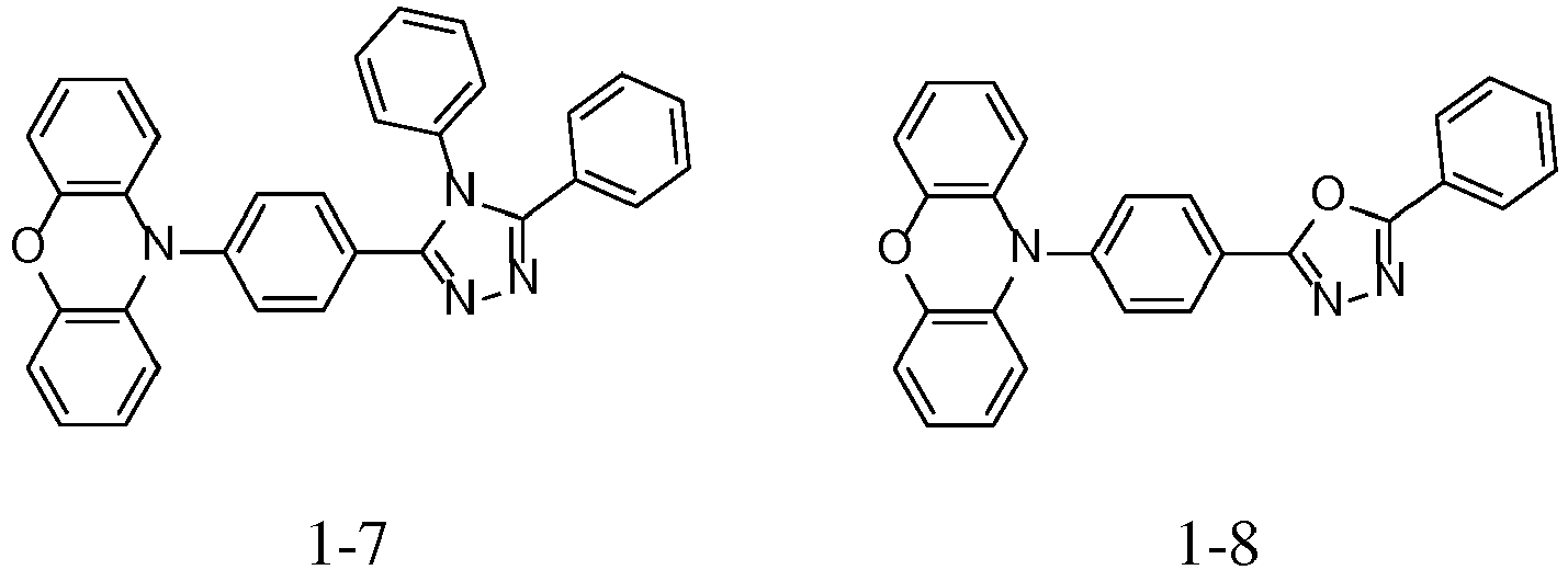


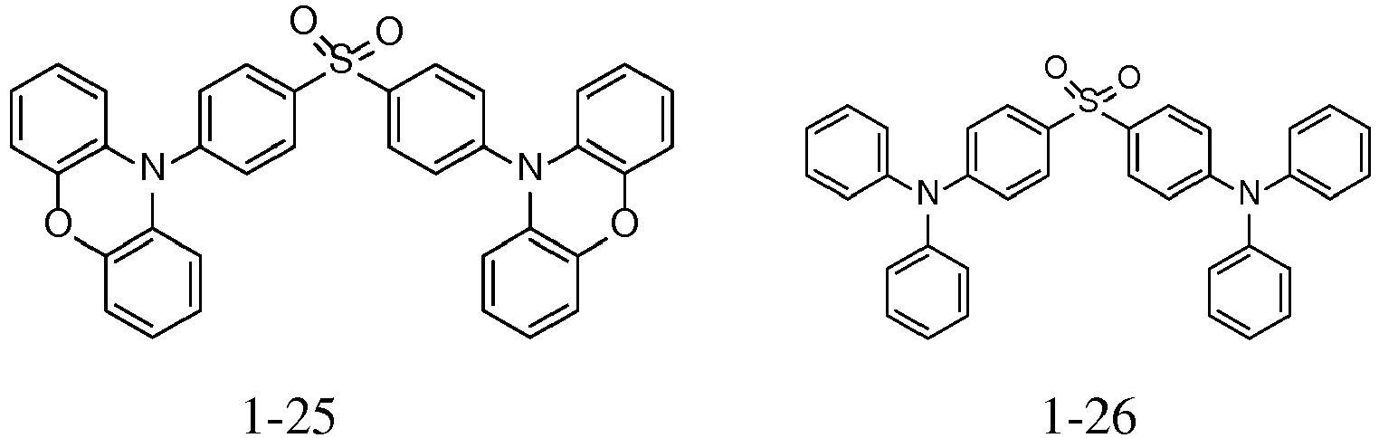


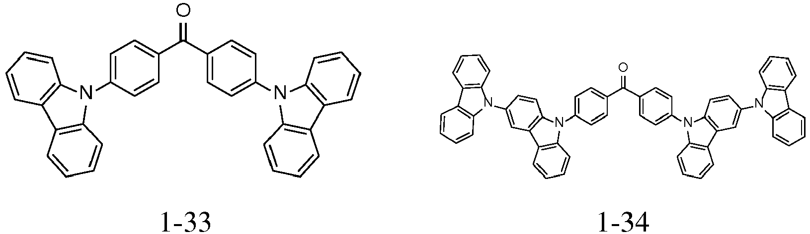


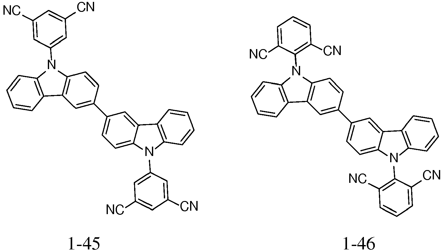

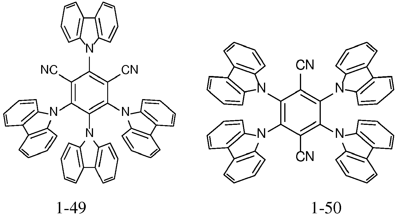


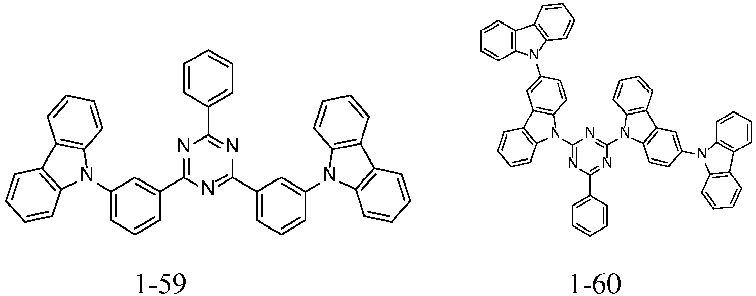

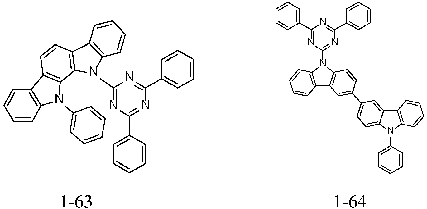


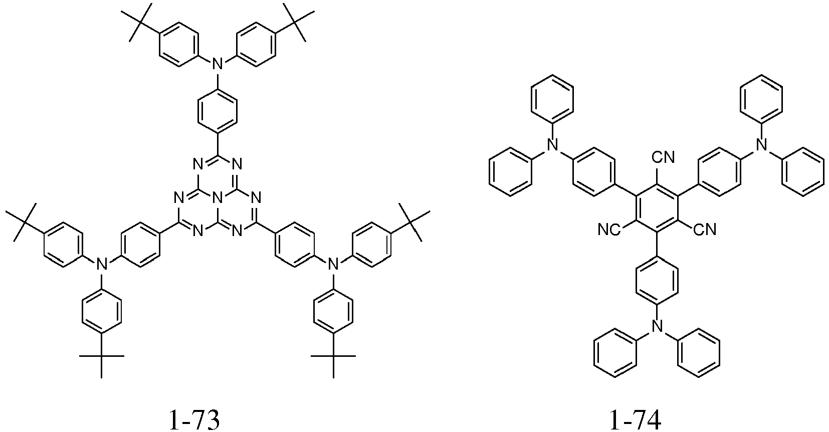


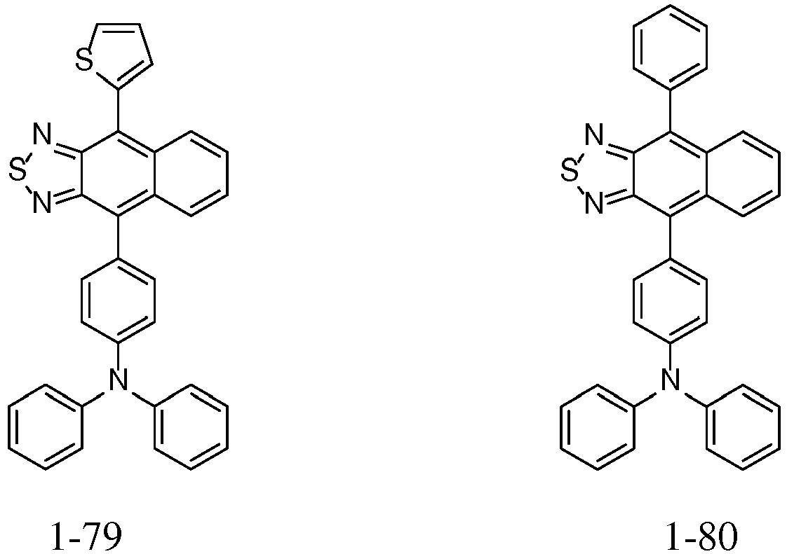

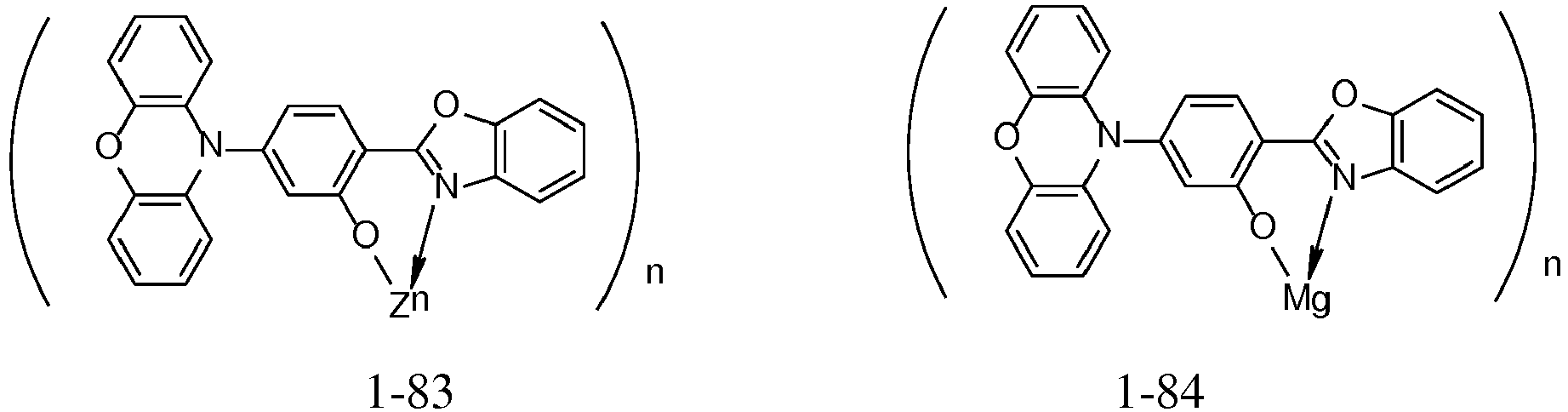


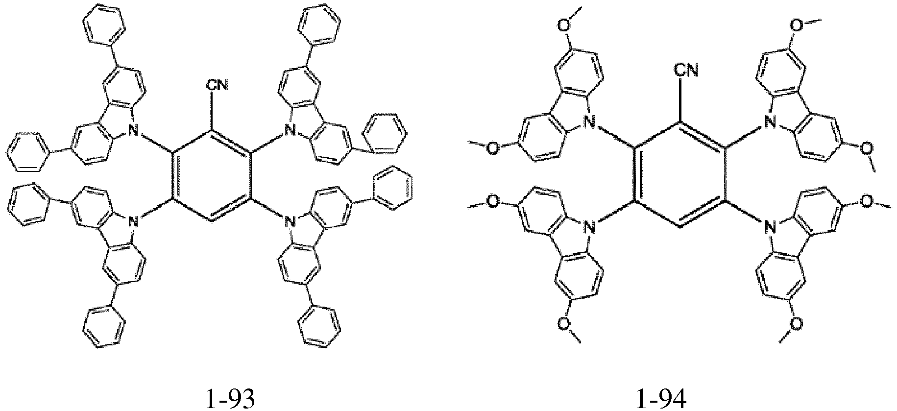


- A preparation method of the organic electroluminescent device of any one of Claims 1-11, comprising the following steps:evaporation coating a first electrode layer (1), a light emitting layer (2) and a second electrode layer (3) in sequence on a substrate by using an open mask;wherein the light emitting layer (2) is prepared by co-evaporation coating of a host material and a dye.
Applications Claiming Priority (2)
| Application Number | Priority Date | Filing Date | Title |
|---|---|---|---|
| CN201510334281.9A CN106328816B (en) | 2015-06-16 | 2015-06-16 | A kind of organic electroluminescence device and preparation method thereof |
| PCT/CN2016/085802 WO2016202251A1 (en) | 2015-06-16 | 2016-06-15 | Organic electroluminescent device and manufacturing method thereof |
Publications (3)
| Publication Number | Publication Date |
|---|---|
| EP3312897A1 true EP3312897A1 (en) | 2018-04-25 |
| EP3312897A4 EP3312897A4 (en) | 2019-04-03 |
| EP3312897B1 EP3312897B1 (en) | 2023-12-27 |
Family
ID=57546627
Family Applications (1)
| Application Number | Title | Priority Date | Filing Date |
|---|---|---|---|
| EP16810992.4A Active EP3312897B1 (en) | 2015-06-16 | 2016-06-15 | Organic electroluminescent device and manufacturing method thereof |
Country Status (7)
| Country | Link |
|---|---|
| US (1) | US11437582B2 (en) |
| EP (1) | EP3312897B1 (en) |
| JP (1) | JP6595627B2 (en) |
| KR (1) | KR102015772B1 (en) |
| CN (1) | CN106328816B (en) |
| TW (1) | TWI634813B (en) |
| WO (1) | WO2016202251A1 (en) |
Cited By (3)
| Publication number | Priority date | Publication date | Assignee | Title |
|---|---|---|---|---|
| EP3739644A2 (en) * | 2019-03-26 | 2020-11-18 | Samsung Display Co., Ltd. | Organic light-emitting device and electronic apparatus |
| US11145827B2 (en) | 2015-08-07 | 2021-10-12 | Semiconductor Energy Laboratory Co., Ltd. | Light-emitting element, display device, electronic device, and lighting device |
| EP3848352A4 (en) * | 2018-09-05 | 2022-06-01 | Kyushu University, National University Corporation | BENZONITRILE DERIVATIVE, ELECTROLUMINESCENT MATERIAL AND ELECTROLUMINESCENT ELEMENT USING THE SAME |
Families Citing this family (44)
| Publication number | Priority date | Publication date | Assignee | Title |
|---|---|---|---|---|
| KR20250105465A (en) * | 2015-07-08 | 2025-07-08 | 가부시키가이샤 한도오따이 에네루기 켄큐쇼 | Light-emitting element, display device, electronic device, and lighting device |
| CN106920883B (en) * | 2015-12-25 | 2019-01-08 | 昆山工研院新型平板显示技术中心有限公司 | A kind of organic electroluminescence device |
| WO2017115834A1 (en) * | 2015-12-28 | 2017-07-06 | 株式会社Kyulux | Compound, light-emitting material, and organic light-emitting device |
| JP6829547B2 (en) * | 2015-12-28 | 2021-02-10 | 株式会社Kyulux | Compounds, light emitting materials and organic light emitting devices |
| CN106220649B (en) * | 2016-04-25 | 2018-07-24 | 中节能万润股份有限公司 | Diaryl ketone-based compound and application thereof in organic electroluminescent device |
| JP2018107449A (en) * | 2016-12-27 | 2018-07-05 | 株式会社半導体エネルギー研究所 | LIGHT EMITTING ELEMENT, LIGHT EMITTING DEVICE, ELECTRONIC DEVICE, AND LIGHTING DEVICE |
| CN108269948B (en) * | 2016-12-30 | 2019-08-16 | 昆山国显光电有限公司 | A kind of host material of organic electroluminescent device and its organic light-emitting layer |
| JP6770900B2 (en) * | 2017-01-12 | 2020-10-21 | 日本放送協会 | Organic electroluminescence element |
| KR102817119B1 (en) * | 2017-01-19 | 2025-06-09 | 삼성디스플레이 주식회사 | Organic electroluminescence device |
| CN108336237B (en) | 2017-01-20 | 2020-01-31 | 昆山工研院新型平板显示技术中心有限公司 | An organic electroluminescent device |
| CN106939000A (en) * | 2017-02-13 | 2017-07-11 | 太原理工大学 | Hot activation delayed fluorescence material based on 1,2,4 triazole acceptors |
| CN108530357A (en) * | 2017-03-03 | 2018-09-14 | 中国科学院宁波材料技术与工程研究所 | Acridine D-A type thermal activation delayed fluorescence material, preparation method and application |
| CN109422735A (en) * | 2017-08-21 | 2019-03-05 | 邱天隆 | Carbazole derivative material and organic light-emitting diode element using same |
| CN107556310B (en) * | 2017-09-20 | 2019-10-22 | 石家庄诚志永华显示材料有限公司 | Imidazole derivative, material containing the same, and organic electroluminescent device |
| WO2019076198A1 (en) * | 2017-10-16 | 2019-04-25 | 北京鼎材科技有限公司 | Compound and organic electroluminescent device |
| KR102083093B1 (en) * | 2017-10-20 | 2020-02-28 | 주식회사 엘지화학 | Organic light emitting device |
| CN112420965B (en) * | 2017-11-18 | 2023-10-24 | 昆山国显光电有限公司 | Organic electroluminescent devices |
| KR102778193B1 (en) * | 2017-11-22 | 2025-03-11 | 삼성전자주식회사 | Composition, thin film and organic light emitting device including the same |
| EP3490023B1 (en) * | 2017-11-22 | 2020-04-22 | Samsung Electronics Co., Ltd. | Composition, thin film including the composition, and organic light-emitting device including the thin film |
| CN108232022A (en) * | 2017-12-29 | 2018-06-29 | 南京邮电大学 | A kind of organic electroluminescence device and preparation method thereof |
| US20210167295A1 (en) * | 2018-04-11 | 2021-06-03 | Nanoco Technologies Ltd. | Electroluminescent display devices and methods of making the same |
| US11367837B2 (en) * | 2018-07-20 | 2022-06-21 | Samsung Electronics Co., Ltd. | Organic light-emitting device |
| CN111372918B (en) | 2018-07-27 | 2023-09-05 | 出光兴产株式会社 | Compound, material for organic electroluminescent element, organic electroluminescent element, and electronic device |
| CN108977197A (en) * | 2018-08-21 | 2018-12-11 | 电子科技大学 | Electroluminescent organic material and preparation method and organic electroluminescence device |
| CN109378392B (en) * | 2018-09-03 | 2020-12-08 | 云谷(固安)科技有限公司 | An organic electroluminescent device and display device |
| WO2020059520A1 (en) * | 2018-09-21 | 2020-03-26 | コニカミノルタ株式会社 | Benzonitrile derivative and manufacturing method therefor, ink composition, organic electroluminescent element material, light-emitting material, charge transport material, light-emitting thin film, and organic electroluminescent element |
| CN118834204A (en) | 2018-12-18 | 2024-10-25 | 阿斯利康(瑞典)有限公司 | Pharmaceutical Processes and Intermediates |
| CN111349040B (en) * | 2018-12-21 | 2023-02-03 | 陕西师范大学 | Organic room temperature phosphorescent and white light emitting material and preparation method thereof |
| CN109713166A (en) * | 2018-12-21 | 2019-05-03 | 苏州大学 | A kind of high-efficiency fluorescence Organic Light Emitting Diode and preparation method thereof |
| KR102752374B1 (en) | 2018-12-27 | 2025-01-08 | 엘지디스플레이 주식회사 | Organic light emitting diode and orgnic light emitting display device including the same |
| CN109678851B (en) * | 2019-01-31 | 2020-08-11 | 武汉华星光电半导体显示技术有限公司 | Thermally activated delayed fluorescence material, organic electroluminescent device and display panel |
| WO2020189330A1 (en) * | 2019-03-19 | 2020-09-24 | コニカミノルタ株式会社 | Functional film, method for forming same, and organic electroluminescent element |
| CN110183361B (en) * | 2019-06-12 | 2021-01-29 | 常州大学 | Construction and application of cross-shaped thermal activity delay fluorescent material |
| CN110437135A (en) * | 2019-08-12 | 2019-11-12 | 三明学院 | D-A-D ' type fluorescent chemicals and synthesis, application |
| CN110627821A (en) * | 2019-09-29 | 2019-12-31 | 上海天马有机发光显示技术有限公司 | Compound, organic electroluminescent device, display panel and display device |
| JP7395136B2 (en) * | 2019-10-10 | 2023-12-11 | 国立大学法人九州大学 | Composition and organic light emitting device |
| US12598914B2 (en) * | 2019-10-18 | 2026-04-07 | Lg Display Co., Ltd. | Organic light emitting diode and organic light emitting device including the same |
| TW202116785A (en) * | 2019-10-28 | 2021-05-01 | 日商東麗股份有限公司 | Light-emitting element material containing pyrromethene boron complex, light-emitting element, display device, and illumination device |
| KR102793989B1 (en) | 2019-11-08 | 2025-04-15 | 삼성디스플레이 주식회사 | Organic electroluminescence device and aromatic compound for organic electroluminescence device |
| CN111916570B (en) * | 2020-06-23 | 2021-08-06 | 华南理工大学 | A TADF-sensitized fluorescent organic light-emitting diode and preparation method thereof |
| KR102875303B1 (en) * | 2020-09-28 | 2025-10-22 | 엘지디스플레이 주식회사 | Organic light emitting diode and organic light emitting device including the same |
| US20220293865A1 (en) * | 2021-03-11 | 2022-09-15 | Universal Display Corporation | Organic electroluminescent materials and devices |
| CN113801102A (en) * | 2021-10-11 | 2021-12-17 | 上海交通大学 | Compounds based on phenazine groups and their preparation methods and applications |
| WO2025159172A1 (en) * | 2024-01-26 | 2025-07-31 | 国立大学法人大阪大学 | Organic electroluminescent element |
Family Cites Families (27)
| Publication number | Priority date | Publication date | Assignee | Title |
|---|---|---|---|---|
| EP2169028B1 (en) * | 2002-03-22 | 2018-11-21 | Idemitsu Kosan Co., Ltd. | Material for organic electroluminescent devices and organic electroluminescent devices made by using the same |
| KR101030158B1 (en) * | 2002-12-23 | 2011-04-18 | 메르크 파텐트 게엠베하 | Organic electroluminescent parts |
| JP4362461B2 (en) * | 2004-11-05 | 2009-11-11 | 三星モバイルディスプレイ株式會社 | Organic electroluminescence device |
| EP2080762B1 (en) * | 2006-11-09 | 2016-09-14 | Nippon Steel & Sumikin Chemical Co., Ltd. | Compound for organic electroluminescent device and organic electroluminescent device |
| CN102017218B (en) * | 2008-05-08 | 2013-05-01 | 新日铁化学株式会社 | Organic electroluminescent element |
| US8632893B2 (en) * | 2008-07-22 | 2014-01-21 | Industrial Technology Research Institute | Organic compound and organic electroluminescence device employing the same |
| EP2403028B1 (en) * | 2009-02-27 | 2014-11-12 | Nippon Steel & Sumikin Chemical Co., Ltd. | Organic electroluminescent element |
| KR101759966B1 (en) * | 2009-03-31 | 2017-07-20 | 신닛테츠 수미킨 가가쿠 가부시키가이샤 | Organic electroluminescent device |
| CN101993440B (en) * | 2009-08-25 | 2012-07-25 | 中国科学院化学研究所 | Benzothiadiazole-based multi-arm conjugated molecules as well as preparation method and application thereof |
| WO2011132683A1 (en) * | 2010-04-20 | 2011-10-27 | 出光興産株式会社 | Bis-carbazole derivative, material for organic electroluminescent element and organic electroluminescent element using same |
| US9954180B2 (en) * | 2010-08-20 | 2018-04-24 | Universal Display Corporation | Bicarbazole compounds for OLEDs |
| TWI549942B (en) | 2010-08-26 | 2016-09-21 | 首威公司 | N-phenyl triscarbazole |
| WO2012133188A1 (en) | 2011-03-25 | 2012-10-04 | 出光興産株式会社 | Organic electroluminescent element |
| JP2015135836A (en) * | 2012-03-29 | 2015-07-27 | 出光興産株式会社 | Organic electroluminescent element and material for organic electroluminescent element |
| JP5594750B2 (en) * | 2012-05-17 | 2014-09-24 | 国立大学法人九州大学 | COMPOUND, LIGHT EMITTING MATERIAL AND ORGANIC LIGHT EMITTING DEVICE |
| CN104411480B (en) | 2012-06-29 | 2016-10-05 | 空中客车营运有限公司 | There is T-shaped longeron and the manufacture method thereof of the web end of rounding |
| JP6339071B2 (en) * | 2012-07-23 | 2018-06-06 | メルク パテント ゲーエムベーハー | Materials for organic electroluminescent devices |
| KR101617877B1 (en) * | 2013-01-16 | 2016-05-03 | 서울대학교산학협력단 | Organic light emitting diode |
| WO2014157610A1 (en) * | 2013-03-29 | 2014-10-02 | コニカミノルタ株式会社 | Organic electroluminescent element, lighting device, display device, light-emitting thin film and composition for organic electroluminescent element, and light-emitting method |
| JP6344382B2 (en) | 2013-04-05 | 2018-06-20 | コニカミノルタ株式会社 | Luminescent layer forming coating liquid, organic electroluminescence element, method for producing the same, and illumination / display device |
| US9365921B2 (en) | 2013-06-28 | 2016-06-14 | Semiconductor Energy Laboratory Co., Ltd. | Method for fabricating light-emitting element using chamber with mass spectrometer |
| WO2015020217A1 (en) | 2013-08-09 | 2015-02-12 | 出光興産株式会社 | Organic electroluminescence composition, material for organic electroluminescence element, solution of material for organic electroluminescence element, and organic electroluminescence element |
| JP5669163B1 (en) * | 2013-08-14 | 2015-02-12 | 国立大学法人九州大学 | Organic electroluminescence device |
| JP5994753B2 (en) | 2013-08-19 | 2016-09-21 | コニカミノルタ株式会社 | ORGANIC ELECTROLUMINESCENT ELEMENT, FLUORESCENT EMITTING COMPOUND USED FOR THE SAME, LIGHTING DEVICE AND DISPLAY DEVICE PROVIDED WITH THE ORGANIC ELECTROLUMINESCENT ELEMENT |
| US9312498B2 (en) | 2013-09-12 | 2016-04-12 | Semiconductor Energy Laboratory Co., Ltd. | Organic compound, light-emitting element, display module, lighting module, light-emitting device, display device, electronic appliance, and lighting device |
| KR102717395B1 (en) * | 2013-12-02 | 2024-10-16 | 가부시키가이샤 한도오따이 에네루기 켄큐쇼 | Light-emitting element, display module, lighting module, light-emitting device, display device, electronic appliance, and lighting device |
| CN104716268B (en) * | 2013-12-17 | 2017-09-29 | 北京维信诺科技有限公司 | A kind of organic electroluminescence device and preparation method thereof |
-
2015
- 2015-06-16 CN CN201510334281.9A patent/CN106328816B/en active Active
-
2016
- 2016-06-15 EP EP16810992.4A patent/EP3312897B1/en active Active
- 2016-06-15 TW TW105118809A patent/TWI634813B/en active
- 2016-06-15 JP JP2017564638A patent/JP6595627B2/en active Active
- 2016-06-15 US US15/737,179 patent/US11437582B2/en active Active
- 2016-06-15 KR KR1020187000314A patent/KR102015772B1/en active Active
- 2016-06-15 WO PCT/CN2016/085802 patent/WO2016202251A1/en not_active Ceased
Cited By (5)
| Publication number | Priority date | Publication date | Assignee | Title |
|---|---|---|---|---|
| US11145827B2 (en) | 2015-08-07 | 2021-10-12 | Semiconductor Energy Laboratory Co., Ltd. | Light-emitting element, display device, electronic device, and lighting device |
| US11770969B2 (en) | 2015-08-07 | 2023-09-26 | Semiconductor Energy Laboratory Co., Ltd. | Light-emitting element, display device, electronic device, and lighting device |
| US12365835B2 (en) | 2015-08-07 | 2025-07-22 | Semiconductor Energy Laboratory Co., Ltd. | Light-emitting element, display device, electronic device, and lighting device |
| EP3848352A4 (en) * | 2018-09-05 | 2022-06-01 | Kyushu University, National University Corporation | BENZONITRILE DERIVATIVE, ELECTROLUMINESCENT MATERIAL AND ELECTROLUMINESCENT ELEMENT USING THE SAME |
| EP3739644A2 (en) * | 2019-03-26 | 2020-11-18 | Samsung Display Co., Ltd. | Organic light-emitting device and electronic apparatus |
Also Published As
| Publication number | Publication date |
|---|---|
| CN106328816B (en) | 2018-11-13 |
| TWI634813B (en) | 2018-09-01 |
| CN106328816A (en) | 2017-01-11 |
| TW201701727A (en) | 2017-01-01 |
| KR20180015242A (en) | 2018-02-12 |
| US11437582B2 (en) | 2022-09-06 |
| US20180175294A1 (en) | 2018-06-21 |
| JP6595627B2 (en) | 2019-10-23 |
| KR102015772B1 (en) | 2019-08-29 |
| EP3312897A4 (en) | 2019-04-03 |
| JP2018519663A (en) | 2018-07-19 |
| EP3312897B1 (en) | 2023-12-27 |
| WO2016202251A1 (en) | 2016-12-22 |
Similar Documents
| Publication | Publication Date | Title |
|---|---|---|
| EP3312897B1 (en) | Organic electroluminescent device and manufacturing method thereof | |
| KR102053569B1 (en) | Multicyclic compound and organic light emitting device comprising the same | |
| EP2097938B1 (en) | Long lifetime phosphorescent organic light emitting device (oled) structures | |
| CN106920884B (en) | A kind of organic electroluminescence device | |
| EP2749625B1 (en) | Organic light emitting diode | |
| CN110838549B (en) | Organic electroluminescent device based on exciplex and exciplex system | |
| TWI530484B (en) | Solution processing doped triarylamine hole injection material | |
| CN112939890A (en) | Heterocyclic organic photoelectric material, preparation method thereof and organic electroluminescent device | |
| WO2017216557A1 (en) | Methods for the production of organic electronic devices | |
| US20180294417A1 (en) | Fluorene-carbazole derivatives and phosphorescent organic electroluminescent devices | |
| US11081646B2 (en) | Coating composition, method for producing organic electroluminescent device using same, and organic electroluminescent device produced thereby | |
| Tang et al. | Transfer printing of polymer light-emitting devices with a small molecular seeding layer featuring thermally activated delayed fluorescence for triplet harvesting | |
| CN115884652B (en) | An organic light-emitting device and panel based on spirofluoreneoxane. | |
| US12495716B2 (en) | Blue luminescent compound, blue luminescent composition, and organic electroluminescent device, display device and lighting device comprising same | |
| CN112961144B (en) | Compound, mixture and organic electroluminescent device | |
| CN112961145A (en) | Compound and organic electroluminescent device | |
| CN109661734B (en) | Organic electroluminescent device and method of manufacturing the same | |
| CN110627684A (en) | Hole injection material, hole injection layer containing hole injection material and OLED display panel | |
| US11158833B2 (en) | Organic electroluminescent device and manufacturing method therefor | |
| CN117693211B (en) | Organic light-emitting diodes and their fabrication methods | |
| CN107056710B (en) | A kind of organic electroluminescent material and organic electroluminescent device | |
| CN114031608B (en) | Phenanthroimidazoles compound and preparation method and application thereof | |
| CN119317309A (en) | Organic light emitting device, display panel and display device | |
| KR20230062319A (en) | Compound for organic light emitting device, Method of Synthesis thereof and organic light emitting device having the same | |
| KR20180007879A (en) | Organic light emitting diode and manufacturing method of the same |
Legal Events
| Date | Code | Title | Description |
|---|---|---|---|
| STAA | Information on the status of an ep patent application or granted ep patent |
Free format text: STATUS: THE INTERNATIONAL PUBLICATION HAS BEEN MADE |
|
| PUAI | Public reference made under article 153(3) epc to a published international application that has entered the european phase |
Free format text: ORIGINAL CODE: 0009012 |
|
| STAA | Information on the status of an ep patent application or granted ep patent |
Free format text: STATUS: REQUEST FOR EXAMINATION WAS MADE |
|
| 17P | Request for examination filed |
Effective date: 20180103 |
|
| AK | Designated contracting states |
Kind code of ref document: A1 Designated state(s): AL AT BE BG CH CY CZ DE DK EE ES FI FR GB GR HR HU IE IS IT LI LT LU LV MC MK MT NL NO PL PT RO RS SE SI SK SM TR |
|
| AX | Request for extension of the european patent |
Extension state: BA ME |
|
| DAV | Request for validation of the european patent (deleted) | ||
| DAX | Request for extension of the european patent (deleted) | ||
| A4 | Supplementary search report drawn up and despatched |
Effective date: 20190301 |
|
| RIC1 | Information provided on ipc code assigned before grant |
Ipc: H01L 51/50 20060101AFI20190225BHEP Ipc: C07D 219/02 20060101ALI20190225BHEP Ipc: C07D 403/10 20060101ALI20190225BHEP Ipc: C07D 221/20 20060101ALI20190225BHEP Ipc: C07D 487/14 20060101ALI20190225BHEP Ipc: C07D 413/14 20060101ALI20190225BHEP |
|
| STAA | Information on the status of an ep patent application or granted ep patent |
Free format text: STATUS: EXAMINATION IS IN PROGRESS |
|
| 17Q | First examination report despatched |
Effective date: 20201222 |
|
| R17C | First examination report despatched (corrected) |
Effective date: 20201222 |
|
| REG | Reference to a national code |
Ref legal event code: R079 Ipc: H10K0050110000 Ref country code: DE Ref document number: 602016085021 Country of ref document: DE Free format text: PREVIOUS MAIN CLASS: H01L0051500000 |
|
| GRAP | Despatch of communication of intention to grant a patent |
Free format text: ORIGINAL CODE: EPIDOSNIGR1 |
|
| RIC1 | Information provided on ipc code assigned before grant |
Ipc: C07D 209/80 20060101ALI20230928BHEP Ipc: H10K 101/20 20230101ALI20230928BHEP Ipc: C07D 285/14 20060101ALI20230928BHEP Ipc: C07D 209/86 20060101ALI20230928BHEP Ipc: H10K 101/00 20230101ALI20230928BHEP Ipc: H10K 101/10 20230101ALI20230928BHEP Ipc: C07D 265/38 20060101ALI20230928BHEP Ipc: C07D 487/16 20060101ALI20230928BHEP Ipc: C07D 471/20 20060101ALI20230928BHEP Ipc: C07D 417/14 20060101ALI20230928BHEP Ipc: C07D 241/48 20060101ALI20230928BHEP Ipc: C07D 417/10 20060101ALI20230928BHEP Ipc: C07D 417/04 20060101ALI20230928BHEP Ipc: C07D 413/10 20060101ALI20230928BHEP Ipc: C07D 403/14 20060101ALI20230928BHEP Ipc: C07D 403/10 20060101ALI20230928BHEP Ipc: C07D 221/20 20060101ALI20230928BHEP Ipc: C07D 219/02 20060101ALI20230928BHEP Ipc: C07D 487/14 20060101ALI20230928BHEP Ipc: C07D 413/14 20060101ALI20230928BHEP Ipc: H10K 50/11 20230101AFI20230928BHEP |
|
| STAA | Information on the status of an ep patent application or granted ep patent |
Free format text: STATUS: GRANT OF PATENT IS INTENDED |
|
| GRAS | Grant fee paid |
Free format text: ORIGINAL CODE: EPIDOSNIGR3 |
|
| GRAA | (expected) grant |
Free format text: ORIGINAL CODE: 0009210 |
|
| STAA | Information on the status of an ep patent application or granted ep patent |
Free format text: STATUS: THE PATENT HAS BEEN GRANTED |
|
| INTG | Intention to grant announced |
Effective date: 20231102 |
|
| RIN1 | Information on inventor provided before grant (corrected) |
Inventor name: ZHAO, FEI Inventor name: XIE, JING Inventor name: LIU, SONG Inventor name: ZHANG, DONGDONG Inventor name: DUAN, LIAN |
|
| AK | Designated contracting states |
Kind code of ref document: B1 Designated state(s): AL AT BE BG CH CY CZ DE DK EE ES FI FR GB GR HR HU IE IS IT LI LT LU LV MC MK MT NL NO PL PT RO RS SE SI SK SM TR |
|
| REG | Reference to a national code |
Ref country code: GB Ref legal event code: FG4D |
|
| REG | Reference to a national code |
Ref country code: CH Ref legal event code: EP |
|
| REG | Reference to a national code |
Ref country code: DE Ref legal event code: R096 Ref document number: 602016085021 Country of ref document: DE |
|
| REG | Reference to a national code |
Ref country code: IE Ref legal event code: FG4D |
|
| PG25 | Lapsed in a contracting state [announced via postgrant information from national office to epo] |
Ref country code: GR Free format text: LAPSE BECAUSE OF FAILURE TO SUBMIT A TRANSLATION OF THE DESCRIPTION OR TO PAY THE FEE WITHIN THE PRESCRIBED TIME-LIMIT Effective date: 20240328 |
|
| REG | Reference to a national code |
Ref country code: LT Ref legal event code: MG9D |
|
| PG25 | Lapsed in a contracting state [announced via postgrant information from national office to epo] |
Ref country code: LT Free format text: LAPSE BECAUSE OF FAILURE TO SUBMIT A TRANSLATION OF THE DESCRIPTION OR TO PAY THE FEE WITHIN THE PRESCRIBED TIME-LIMIT Effective date: 20231227 |
|
| PG25 | Lapsed in a contracting state [announced via postgrant information from national office to epo] |
Ref country code: ES Free format text: LAPSE BECAUSE OF FAILURE TO SUBMIT A TRANSLATION OF THE DESCRIPTION OR TO PAY THE FEE WITHIN THE PRESCRIBED TIME-LIMIT Effective date: 20231227 |
|
| PG25 | Lapsed in a contracting state [announced via postgrant information from national office to epo] |
Ref country code: LT Free format text: LAPSE BECAUSE OF FAILURE TO SUBMIT A TRANSLATION OF THE DESCRIPTION OR TO PAY THE FEE WITHIN THE PRESCRIBED TIME-LIMIT Effective date: 20231227 Ref country code: GR Free format text: LAPSE BECAUSE OF FAILURE TO SUBMIT A TRANSLATION OF THE DESCRIPTION OR TO PAY THE FEE WITHIN THE PRESCRIBED TIME-LIMIT Effective date: 20240328 Ref country code: FI Free format text: LAPSE BECAUSE OF FAILURE TO SUBMIT A TRANSLATION OF THE DESCRIPTION OR TO PAY THE FEE WITHIN THE PRESCRIBED TIME-LIMIT Effective date: 20231227 Ref country code: ES Free format text: LAPSE BECAUSE OF FAILURE TO SUBMIT A TRANSLATION OF THE DESCRIPTION OR TO PAY THE FEE WITHIN THE PRESCRIBED TIME-LIMIT Effective date: 20231227 Ref country code: BG Free format text: LAPSE BECAUSE OF FAILURE TO SUBMIT A TRANSLATION OF THE DESCRIPTION OR TO PAY THE FEE WITHIN THE PRESCRIBED TIME-LIMIT Effective date: 20240327 |
|
| REG | Reference to a national code |
Ref country code: NL Ref legal event code: MP Effective date: 20231227 |
|
| REG | Reference to a national code |
Ref country code: AT Ref legal event code: MK05 Ref document number: 1645781 Country of ref document: AT Kind code of ref document: T Effective date: 20231227 |
|
| PG25 | Lapsed in a contracting state [announced via postgrant information from national office to epo] |
Ref country code: NL Free format text: LAPSE BECAUSE OF FAILURE TO SUBMIT A TRANSLATION OF THE DESCRIPTION OR TO PAY THE FEE WITHIN THE PRESCRIBED TIME-LIMIT Effective date: 20231227 |
|
| PG25 | Lapsed in a contracting state [announced via postgrant information from national office to epo] |
Ref country code: SE Free format text: LAPSE BECAUSE OF FAILURE TO SUBMIT A TRANSLATION OF THE DESCRIPTION OR TO PAY THE FEE WITHIN THE PRESCRIBED TIME-LIMIT Effective date: 20231227 Ref country code: RS Free format text: LAPSE BECAUSE OF FAILURE TO SUBMIT A TRANSLATION OF THE DESCRIPTION OR TO PAY THE FEE WITHIN THE PRESCRIBED TIME-LIMIT Effective date: 20231227 Ref country code: NO Free format text: LAPSE BECAUSE OF FAILURE TO SUBMIT A TRANSLATION OF THE DESCRIPTION OR TO PAY THE FEE WITHIN THE PRESCRIBED TIME-LIMIT Effective date: 20240327 Ref country code: NL Free format text: LAPSE BECAUSE OF FAILURE TO SUBMIT A TRANSLATION OF THE DESCRIPTION OR TO PAY THE FEE WITHIN THE PRESCRIBED TIME-LIMIT Effective date: 20231227 Ref country code: LV Free format text: LAPSE BECAUSE OF FAILURE TO SUBMIT A TRANSLATION OF THE DESCRIPTION OR TO PAY THE FEE WITHIN THE PRESCRIBED TIME-LIMIT Effective date: 20231227 Ref country code: HR Free format text: LAPSE BECAUSE OF FAILURE TO SUBMIT A TRANSLATION OF THE DESCRIPTION OR TO PAY THE FEE WITHIN THE PRESCRIBED TIME-LIMIT Effective date: 20231227 |
|
| PG25 | Lapsed in a contracting state [announced via postgrant information from national office to epo] |
Ref country code: IS Free format text: LAPSE BECAUSE OF FAILURE TO SUBMIT A TRANSLATION OF THE DESCRIPTION OR TO PAY THE FEE WITHIN THE PRESCRIBED TIME-LIMIT Effective date: 20240427 |
|
| PG25 | Lapsed in a contracting state [announced via postgrant information from national office to epo] |
Ref country code: CZ Free format text: LAPSE BECAUSE OF FAILURE TO SUBMIT A TRANSLATION OF THE DESCRIPTION OR TO PAY THE FEE WITHIN THE PRESCRIBED TIME-LIMIT Effective date: 20231227 Ref country code: AT Free format text: LAPSE BECAUSE OF FAILURE TO SUBMIT A TRANSLATION OF THE DESCRIPTION OR TO PAY THE FEE WITHIN THE PRESCRIBED TIME-LIMIT Effective date: 20231227 |
|
| PG25 | Lapsed in a contracting state [announced via postgrant information from national office to epo] |
Ref country code: SK Free format text: LAPSE BECAUSE OF FAILURE TO SUBMIT A TRANSLATION OF THE DESCRIPTION OR TO PAY THE FEE WITHIN THE PRESCRIBED TIME-LIMIT Effective date: 20231227 |
|
| PG25 | Lapsed in a contracting state [announced via postgrant information from national office to epo] |
Ref country code: SM Free format text: LAPSE BECAUSE OF FAILURE TO SUBMIT A TRANSLATION OF THE DESCRIPTION OR TO PAY THE FEE WITHIN THE PRESCRIBED TIME-LIMIT Effective date: 20231227 Ref country code: SK Free format text: LAPSE BECAUSE OF FAILURE TO SUBMIT A TRANSLATION OF THE DESCRIPTION OR TO PAY THE FEE WITHIN THE PRESCRIBED TIME-LIMIT Effective date: 20231227 Ref country code: RO Free format text: LAPSE BECAUSE OF FAILURE TO SUBMIT A TRANSLATION OF THE DESCRIPTION OR TO PAY THE FEE WITHIN THE PRESCRIBED TIME-LIMIT Effective date: 20231227 Ref country code: IT Free format text: LAPSE BECAUSE OF FAILURE TO SUBMIT A TRANSLATION OF THE DESCRIPTION OR TO PAY THE FEE WITHIN THE PRESCRIBED TIME-LIMIT Effective date: 20231227 Ref country code: IS Free format text: LAPSE BECAUSE OF FAILURE TO SUBMIT A TRANSLATION OF THE DESCRIPTION OR TO PAY THE FEE WITHIN THE PRESCRIBED TIME-LIMIT Effective date: 20240427 Ref country code: EE Free format text: LAPSE BECAUSE OF FAILURE TO SUBMIT A TRANSLATION OF THE DESCRIPTION OR TO PAY THE FEE WITHIN THE PRESCRIBED TIME-LIMIT Effective date: 20231227 Ref country code: CZ Free format text: LAPSE BECAUSE OF FAILURE TO SUBMIT A TRANSLATION OF THE DESCRIPTION OR TO PAY THE FEE WITHIN THE PRESCRIBED TIME-LIMIT Effective date: 20231227 Ref country code: AT Free format text: LAPSE BECAUSE OF FAILURE TO SUBMIT A TRANSLATION OF THE DESCRIPTION OR TO PAY THE FEE WITHIN THE PRESCRIBED TIME-LIMIT Effective date: 20231227 |
|
| PG25 | Lapsed in a contracting state [announced via postgrant information from national office to epo] |
Ref country code: PT Free format text: LAPSE BECAUSE OF FAILURE TO SUBMIT A TRANSLATION OF THE DESCRIPTION OR TO PAY THE FEE WITHIN THE PRESCRIBED TIME-LIMIT Effective date: 20240429 Ref country code: PL Free format text: LAPSE BECAUSE OF FAILURE TO SUBMIT A TRANSLATION OF THE DESCRIPTION OR TO PAY THE FEE WITHIN THE PRESCRIBED TIME-LIMIT Effective date: 20231227 |
|
| PG25 | Lapsed in a contracting state [announced via postgrant information from national office to epo] |
Ref country code: PT Free format text: LAPSE BECAUSE OF FAILURE TO SUBMIT A TRANSLATION OF THE DESCRIPTION OR TO PAY THE FEE WITHIN THE PRESCRIBED TIME-LIMIT Effective date: 20240429 Ref country code: PL Free format text: LAPSE BECAUSE OF FAILURE TO SUBMIT A TRANSLATION OF THE DESCRIPTION OR TO PAY THE FEE WITHIN THE PRESCRIBED TIME-LIMIT Effective date: 20231227 |
|
| REG | Reference to a national code |
Ref country code: DE Ref legal event code: R097 Ref document number: 602016085021 Country of ref document: DE |
|
| PG25 | Lapsed in a contracting state [announced via postgrant information from national office to epo] |
Ref country code: DK Free format text: LAPSE BECAUSE OF FAILURE TO SUBMIT A TRANSLATION OF THE DESCRIPTION OR TO PAY THE FEE WITHIN THE PRESCRIBED TIME-LIMIT Effective date: 20231227 |
|
| PG25 | Lapsed in a contracting state [announced via postgrant information from national office to epo] |
Ref country code: DK Free format text: LAPSE BECAUSE OF FAILURE TO SUBMIT A TRANSLATION OF THE DESCRIPTION OR TO PAY THE FEE WITHIN THE PRESCRIBED TIME-LIMIT Effective date: 20231227 |
|
| PLBE | No opposition filed within time limit |
Free format text: ORIGINAL CODE: 0009261 |
|
| STAA | Information on the status of an ep patent application or granted ep patent |
Free format text: STATUS: NO OPPOSITION FILED WITHIN TIME LIMIT |
|
| 26N | No opposition filed |
Effective date: 20240930 |
|
| PG25 | Lapsed in a contracting state [announced via postgrant information from national office to epo] |
Ref country code: MC Free format text: LAPSE BECAUSE OF FAILURE TO SUBMIT A TRANSLATION OF THE DESCRIPTION OR TO PAY THE FEE WITHIN THE PRESCRIBED TIME-LIMIT Effective date: 20231227 |
|
| REG | Reference to a national code |
Ref country code: CH Ref legal event code: PL |
|
| PG25 | Lapsed in a contracting state [announced via postgrant information from national office to epo] |
Ref country code: LU Free format text: LAPSE BECAUSE OF NON-PAYMENT OF DUE FEES Effective date: 20240615 |
|
| PG25 | Lapsed in a contracting state [announced via postgrant information from national office to epo] |
Ref country code: IE Free format text: LAPSE BECAUSE OF NON-PAYMENT OF DUE FEES Effective date: 20240615 |
|
| PG25 | Lapsed in a contracting state [announced via postgrant information from national office to epo] |
Ref country code: SI Free format text: LAPSE BECAUSE OF FAILURE TO SUBMIT A TRANSLATION OF THE DESCRIPTION OR TO PAY THE FEE WITHIN THE PRESCRIBED TIME-LIMIT Effective date: 20231227 Ref country code: CH Free format text: LAPSE BECAUSE OF NON-PAYMENT OF DUE FEES Effective date: 20240630 Ref country code: BE Free format text: LAPSE BECAUSE OF NON-PAYMENT OF DUE FEES Effective date: 20240630 |
|
| REG | Reference to a national code |
Ref country code: BE Ref legal event code: MM Effective date: 20240630 |
|
| PGFP | Annual fee paid to national office [announced via postgrant information from national office to epo] |
Ref country code: DE Payment date: 20250617 Year of fee payment: 10 |
|
| PGFP | Annual fee paid to national office [announced via postgrant information from national office to epo] |
Ref country code: GB Payment date: 20250625 Year of fee payment: 10 |
|
| PGFP | Annual fee paid to national office [announced via postgrant information from national office to epo] |
Ref country code: FR Payment date: 20250630 Year of fee payment: 10 |
|
| PG25 | Lapsed in a contracting state [announced via postgrant information from national office to epo] |
Ref country code: CY Free format text: LAPSE BECAUSE OF FAILURE TO SUBMIT A TRANSLATION OF THE DESCRIPTION OR TO PAY THE FEE WITHIN THE PRESCRIBED TIME-LIMIT; INVALID AB INITIO Effective date: 20160615 |
|
| PG25 | Lapsed in a contracting state [announced via postgrant information from national office to epo] |
Ref country code: HU Free format text: LAPSE BECAUSE OF FAILURE TO SUBMIT A TRANSLATION OF THE DESCRIPTION OR TO PAY THE FEE WITHIN THE PRESCRIBED TIME-LIMIT; INVALID AB INITIO Effective date: 20160615 |