EP3308484B1 - Macro-commutateur ayant une matrice de commutation à mémoire tampon - Google Patents
Macro-commutateur ayant une matrice de commutation à mémoire tampon Download PDFInfo
- Publication number
- EP3308484B1 EP3308484B1 EP16734775.6A EP16734775A EP3308484B1 EP 3308484 B1 EP3308484 B1 EP 3308484B1 EP 16734775 A EP16734775 A EP 16734775A EP 3308484 B1 EP3308484 B1 EP 3308484B1
- Authority
- EP
- European Patent Office
- Prior art keywords
- switch
- optical
- macro
- given
- sites
- Prior art date
- Legal status (The legal status is an assumption and is not a legal conclusion. Google has not performed a legal analysis and makes no representation as to the accuracy of the status listed.)
- Active
Links
- 239000011159 matrix material Substances 0.000 title description 5
- 230000003287 optical effect Effects 0.000 claims description 166
- 239000000872 buffer Substances 0.000 claims description 28
- 230000000903 blocking effect Effects 0.000 claims description 18
- 238000000034 method Methods 0.000 claims description 18
- 239000004065 semiconductor Substances 0.000 claims description 13
- 239000000758 substrate Substances 0.000 claims description 13
- 238000004891 communication Methods 0.000 claims description 11
- 230000008878 coupling Effects 0.000 claims description 8
- 238000010168 coupling process Methods 0.000 claims description 8
- 238000005859 coupling reaction Methods 0.000 claims description 8
- 238000005516 engineering process Methods 0.000 claims description 4
- 239000012212 insulator Substances 0.000 claims description 3
- 239000013307 optical fiber Substances 0.000 description 17
- 238000010586 diagram Methods 0.000 description 11
- XUIMIQQOPSSXEZ-UHFFFAOYSA-N Silicon Chemical compound [Si] XUIMIQQOPSSXEZ-UHFFFAOYSA-N 0.000 description 8
- 230000002457 bidirectional effect Effects 0.000 description 8
- 229910052710 silicon Inorganic materials 0.000 description 8
- 239000010703 silicon Substances 0.000 description 8
- 239000000463 material Substances 0.000 description 6
- VYPSYNLAJGMNEJ-UHFFFAOYSA-N Silicium dioxide Chemical compound O=[Si]=O VYPSYNLAJGMNEJ-UHFFFAOYSA-N 0.000 description 4
- 238000012545 processing Methods 0.000 description 4
- 239000000203 mixture Substances 0.000 description 3
- 238000003860 storage Methods 0.000 description 3
- 238000013459 approach Methods 0.000 description 2
- 230000003139 buffering effect Effects 0.000 description 2
- 150000001875 compounds Chemical class 0.000 description 2
- 238000004590 computer program Methods 0.000 description 2
- 238000013461 design Methods 0.000 description 2
- 230000006870 function Effects 0.000 description 2
- 230000008569 process Effects 0.000 description 2
- 235000012239 silicon dioxide Nutrition 0.000 description 2
- 239000000377 silicon dioxide Substances 0.000 description 2
- 239000000654 additive Substances 0.000 description 1
- 230000000996 additive effect Effects 0.000 description 1
- 229910021417 amorphous silicon Inorganic materials 0.000 description 1
- 238000003491 array Methods 0.000 description 1
- 230000005540 biological transmission Effects 0.000 description 1
- 230000001413 cellular effect Effects 0.000 description 1
- 230000008859 change Effects 0.000 description 1
- 238000005229 chemical vapour deposition Methods 0.000 description 1
- 238000001816 cooling Methods 0.000 description 1
- 230000003247 decreasing effect Effects 0.000 description 1
- 238000000151 deposition Methods 0.000 description 1
- 230000008021 deposition Effects 0.000 description 1
- 238000009826 distribution Methods 0.000 description 1
- 238000001312 dry etching Methods 0.000 description 1
- 230000008020 evaporation Effects 0.000 description 1
- 238000001704 evaporation Methods 0.000 description 1
- 239000000835 fiber Substances 0.000 description 1
- 239000011521 glass Substances 0.000 description 1
- 229910010272 inorganic material Inorganic materials 0.000 description 1
- 239000011147 inorganic material Substances 0.000 description 1
- 238000001459 lithography Methods 0.000 description 1
- 238000013507 mapping Methods 0.000 description 1
- 230000007246 mechanism Effects 0.000 description 1
- 239000002184 metal Substances 0.000 description 1
- 238000012986 modification Methods 0.000 description 1
- 230000004048 modification Effects 0.000 description 1
- 238000001451 molecular beam epitaxy Methods 0.000 description 1
- 239000011368 organic material Substances 0.000 description 1
- 238000000206 photolithography Methods 0.000 description 1
- 238000005498 polishing Methods 0.000 description 1
- 229910021420 polycrystalline silicon Inorganic materials 0.000 description 1
- 229920000642 polymer Polymers 0.000 description 1
- 229920005591 polysilicon Polymers 0.000 description 1
- 239000011347 resin Substances 0.000 description 1
- 229920005989 resin Polymers 0.000 description 1
- 229910052594 sapphire Inorganic materials 0.000 description 1
- 239000010980 sapphire Substances 0.000 description 1
- 238000004544 sputter deposition Methods 0.000 description 1
- 238000005303 weighing Methods 0.000 description 1
- 238000001039 wet etching Methods 0.000 description 1
Images


Classifications
-
- H—ELECTRICITY
- H04—ELECTRIC COMMUNICATION TECHNIQUE
- H04Q—SELECTING
- H04Q11/00—Selecting arrangements for multiplex systems
- H04Q11/0001—Selecting arrangements for multiplex systems using optical switching
- H04Q11/0062—Network aspects
-
- H—ELECTRICITY
- H04—ELECTRIC COMMUNICATION TECHNIQUE
- H04Q—SELECTING
- H04Q11/00—Selecting arrangements for multiplex systems
- H04Q11/0001—Selecting arrangements for multiplex systems using optical switching
- H04Q11/0005—Switch and router aspects
-
- G—PHYSICS
- G02—OPTICS
- G02B—OPTICAL ELEMENTS, SYSTEMS OR APPARATUS
- G02B6/00—Light guides; Structural details of arrangements comprising light guides and other optical elements, e.g. couplings
- G02B6/24—Coupling light guides
- G02B6/26—Optical coupling means
- G02B6/35—Optical coupling means having switching means
- G02B6/354—Switching arrangements, i.e. number of input/output ports and interconnection types
- G02B6/3542—Non-blocking switch, e.g. with multiple potential paths between multiple inputs and outputs, the establishment of one switching path not preventing the establishment of further switching paths
-
- G—PHYSICS
- G02—OPTICS
- G02B—OPTICAL ELEMENTS, SYSTEMS OR APPARATUS
- G02B6/00—Light guides; Structural details of arrangements comprising light guides and other optical elements, e.g. couplings
- G02B6/24—Coupling light guides
- G02B6/26—Optical coupling means
- G02B6/35—Optical coupling means having switching means
- G02B6/3596—With planar waveguide arrangement, i.e. in a substrate, regardless if actuating mechanism is outside the substrate
-
- H—ELECTRICITY
- H04—ELECTRIC COMMUNICATION TECHNIQUE
- H04B—TRANSMISSION
- H04B10/00—Transmission systems employing electromagnetic waves other than radio-waves, e.g. infrared, visible or ultraviolet light, or employing corpuscular radiation, e.g. quantum communication
- H04B10/25—Arrangements specific to fibre transmission
- H04B10/2589—Bidirectional transmission
- H04B10/25891—Transmission components
-
- H—ELECTRICITY
- H04—ELECTRIC COMMUNICATION TECHNIQUE
- H04B—TRANSMISSION
- H04B10/00—Transmission systems employing electromagnetic waves other than radio-waves, e.g. infrared, visible or ultraviolet light, or employing corpuscular radiation, e.g. quantum communication
- H04B10/40—Transceivers
-
- H—ELECTRICITY
- H04—ELECTRIC COMMUNICATION TECHNIQUE
- H04J—MULTIPLEX COMMUNICATION
- H04J14/00—Optical multiplex systems
- H04J14/02—Wavelength-division multiplex systems
-
- H—ELECTRICITY
- H04—ELECTRIC COMMUNICATION TECHNIQUE
- H04J—MULTIPLEX COMMUNICATION
- H04J14/00—Optical multiplex systems
- H04J14/02—Wavelength-division multiplex systems
- H04J14/0201—Add-and-drop multiplexing
- H04J14/0202—Arrangements therefor
- H04J14/021—Reconfigurable arrangements, e.g. reconfigurable optical add/drop multiplexers [ROADM] or tunable optical add/drop multiplexers [TOADM]
- H04J14/0212—Reconfigurable arrangements, e.g. reconfigurable optical add/drop multiplexers [ROADM] or tunable optical add/drop multiplexers [TOADM] using optical switches or wavelength selective switches [WSS]
-
- H—ELECTRICITY
- H04—ELECTRIC COMMUNICATION TECHNIQUE
- H04Q—SELECTING
- H04Q11/00—Selecting arrangements for multiplex systems
- H04Q11/0001—Selecting arrangements for multiplex systems using optical switching
- H04Q11/0005—Switch and router aspects
- H04Q2011/0037—Operation
- H04Q2011/005—Arbitration and scheduling
-
- H—ELECTRICITY
- H04—ELECTRIC COMMUNICATION TECHNIQUE
- H04Q—SELECTING
- H04Q11/00—Selecting arrangements for multiplex systems
- H04Q11/0001—Selecting arrangements for multiplex systems using optical switching
- H04Q11/0062—Network aspects
- H04Q2011/009—Topology aspects
Definitions
- the present disclosure relates to techniques for communicating optical signals. More specifically, the present disclosure relates to an optical cross-point macro-switch with a buffered switching matrix.
- Multistage Clos packet-switching networks are widely used in computing and telecommunications switching and routing systems to provide shared interconnectivity among many distinct endpoints or ports in these systems.
- these packet-switching networks are typically implemented as space-division switches that can scale to thousands of ports.
- This contention can be removed by using buffered switching nodes within each stage, so that all the intermediate nodes can store packets, thereby alleviating head-of-line blocking and/or output port blocking.
- Such memory buffers may also be used before and/or after the network in order to reduce head-of-line blocking, as well as to reduce switch contention because of output port blocking.
- efficiency of the network is generally limited, and careful (and relatively complex) scheduling techniques may be needed to ensure that the network is not overloaded or pushed past its critical loading into an inefficient operating regime.
- each stage may have not only routing and forwarding functionality, but may also have memory buffers and rich connectivity to preceding and following switching/routing stages.
- the need for memory at each stage may directly compete with the number of switches per stage and the number of stages that can be implemented. Therefore, the use of memory buffers at all stages in the switch may constrain the scalability of the switch.
- optical interconnects in VLSI switches can provide high-speed communication, and may permit large Clos packet-switching networks to be aggregated, e.g., by connecting smaller electrical switches with optical fiber links. While this architecture may facilitate the implementation of larger Clos packet-switching networks, it typically does not change the nature of the switching contention discussed previously. Indeed, the resulting Clos packet-switching networks usually have all the same congestion and inefficiencies, just at a larger scale.
- photonic-switching (or optical-switching) products can eliminate the electrical switching stage in favor of a 'transparent' optical switch, in which data packets are sent via beams of light from any input port to an arbitrary output port. While the speed and latency of transmission of these photonic-switching products are low, the input port and the output port contention issues (and, thus, the inefficiencies) remain.
- US7356213 discloses a switch which includes input ports configured to receive signals (which include data) and output ports configured to output the signals.
- US 2009/003827 discloses An optical switching device the size and costs of which are reduced by decreasing the number of switching elements and which can flexibly accommodate the expansion of the number of ports.
- US 2011/255822 discloses an optical switch that includes two optical waveguides.
- One embodiment of the present disclosure provides a macro-switch that includes a first integrated circuit.
- This first integrated circuit has a surface and includes: first switch sites, where each of the first switch sites includes first control logic and a first memory buffer; and second switch sites, where each of the second switch sites includes second control logic and a second memory buffer.
- the macro-switch includes a second integrated circuit having a second surface facing the surface.
- the second integrated circuit includes: optical ports that can be coupled to optical sources; optical waveguides optically coupled to the optical ports and the first switch sites; and second optical waveguides optically coupled to the first switch sites and the second switch sites. Note that the macro-switch has a fully connected topology between the first switch sites and the second switch sites.
- the macro-switch may include a cross-point switch.
- the macro-switch may be non-blocking.
- the first control logic at a given first switch site may determine a given first switching schedule for the given first switch site
- the second control logic at the given second switch site may determine a given second switching schedule for the given second switch site.
- the given first switching schedule may be determined independently from other switching schedules for the first switch sites and the second switch sites
- the given second switching schedule may be determined independently from the other switching schedules for the first switch sites and the second switch sites.
- the optical waveguides between a given optical port and a given first switch site may include one optical waveguide that, during operation, conveys information from the given optical port to the given first switch site and another optical waveguide that, during operation, conveys information from the given first switch site to the given optical port.
- the second optical waveguides between a given first switch site and the given second switch site may include one optical waveguide that, during operation, conveys information from the given first switch site to the given second switch site and another optical waveguide that, during operation, conveys information from the given second switch site to the given first switch site.
- optical coupling may involve: a diffraction grating, a mirror, and/or optical proximity communication.
- the given first switch site may include transceivers that, during operation, convert input optical signals into input electrical signals and output electrical signals into output optical signals.
- the given second switch site may include second transceivers that, during operation, convert second input optical signals into second input electrical signals and second output electrical signals into second output optical signals.
- the second integrated circuit includes: a substrate; a buried-oxide ( BOX ) layer disposed on the substrate; and a semiconductor layer disposed on the BOX layer, where the optical waveguides and the second optical waveguides are, at least in part, implemented in the semiconductor layer.
- the substrate, the BOX layer and the semiconductor layer may constitute a silicon-on-insulator technology.
- Another embodiment provides a system that includes: a processor; a memory that stores a program module; and the macro-switch. During operation, the program module is executed by the processor.
- Another embodiment provides a method for switching optical signals using a macro-switch.
- the macro-switch conveys optical signals in optical waveguides in a second integrated circuit in the macro-switch.
- the macro-switch optically couples the optical signals from the optical waveguide to and from switch sites in a first integrated circuit in the macro-switch, where a given switch site includes control logic and a memory buffer, and where the control logic determines a switching schedule independently of other switch sites in the macro-switch.
- the macro-switch converts an optical signal to an electrical signal, performs switching, and converts the electrical signal into the optical signal, where the electrical signal is selectively stored in the memory buffer to avoid contention in the macro-switch.
- Embodiments of a macro-switch, a system that includes the macro-switch, and a technique for switching optical signals using the macro-switch are described.
- the macro-switch may include facing integrated circuits, one of which implements optical waveguides that convey optical signals, and the other which implements control logic, electrical switches and memory buffers at each of multiple switch sites.
- the macro-switch may have a fully connected topology between the switch sites.
- the memory buffers at each switch site provide packet buffering and congestion relief without causing undue scheduling/routing complexity.
- the macro-switch can be scaled to an arbitrarily large switching matrix (i.e., an arbitrary number of switch sites and/or switching stages).
- the macro-switch may have a 4096x4096 switching matrix (which is 6,700x larger than existing photonic switches).
- the macro-switch may have a small footprint and improved switch performance.
- the macro-switch may provide a low-power, high-bandwidth non-blocking electro-optical switch-on-a-chip.
- a folded-Clos (fat-tree) packet-switching network is used as an illustration in the macro-switch.
- the switching technique may be used with a wide variety of switch designs and architectures.
- FIG. 1 presents a block diagram illustrating a top view of a macro-switch 100, with integrated circuits 110 and 112.
- Integrated circuit 110 may include: multiple switch sites 114 (which are sometimes referred to as 'leaf switch sites') that each include or are associated with instances of control logic ( C.L. ) 116 and memory buffers ( M.B. ) 118; and multiple switch sites 120 (which are sometimes referred to as 'spine switch sites') that each include or are associated with instances of control logic ( C.L. ) 122 and memory buffers ( M.B. ) 124.
- integrated circuit 112 may include optical waveguides 126 and 128.
- optical waveguides may optically couple optical ports ( O.P .) 130 (which can be optically coupled to optical fibers or additional optical waveguides, and more generally to sources and sinks of optical signals) and switch sites 114. Furthermore, optical waveguides 128 may optically couple switch sites 114 and 120.
- FIG. 2 which presents a block diagram illustrating a side view of macro-switch 100
- integrated circuits 110 and 112 have surfaces 210 and 212 that face each other.
- a given switch site in switch sites 114 in FIG. 1 (such as switch site 114-1) may be optically coupled to a given one of optical ports 130 in FIG. 1 (such as optical port 130-1) by at least one of optical waveguides 126 in FIG. 1 (such as optical waveguide 126-1 in FIG. 2 ).
- optical waveguides 126 and 128 may convey optical signals unidirectionally. (However, in other embodiments optical waveguides 126 and 128 in FIG. 1 convey optical signals bidirectionally.)
- Input optical signals may be optically coupled from integrated circuit 112 to integrated circuit 110 by optical couplers.
- an input optical signal conveyed using optical waveguide 126-1 may be optically coupled to switch site 114-1 by optical coupler ( O.C .) 210-1.
- This optical coupler may include a diffraction grating and/or a mirror.
- the optical coupling involves optical proximity communication, in which a vertical spacing between integrated circuits 110 and 112 is less than or on the same order as one or more carrier wavelengths of optical signals that are optically coupled between integrated circuits 110 and 112.
- the input optical signals may be converted into electrical signals by transceivers.
- the input optical signal from optical coupler 210-1 may be converted into an electrical signal by transceiver ( TR .) 212-1.
- transceiver TR .
- one or more packets associated with this electrical signal may be processed by an instance of control logic 116 ( FIG. 1 ) and may be selectively stored in an instance of memory buffers 118 ( FIG. 1 ) to avoid contention in macro-switch 100.
- the instance of control logic 116 may: set an appropriate routing or switching state of a switch at switch site 114-1 (such as switch 132-1 in switches (SW.) 132 in FIG. 1 ); optionally access the packet in the instance of memory buffers 118 ( FIG. 1 ); and output an associated electrical signal.
- This electrical signal may be converted into an optical signal by transceiver 212-2.
- this optical signal may be optically coupled from integrated circuit 110 into at least one of optical waveguides 128 in FIG. 1 (such as optical waveguide 128-1 in FIG. 2 ) by optical coupler 210-2. Then, optical waveguide 128-1 may convey the optical signal to a given switch site in switch sites 120 in FIG. 1 (such as switch site 120-1).
- the optical signal may be optically coupled from integrated circuit 112 to switch site 120-1 by optical coupler 210-3. Furthermore, at switch sites 120-1, the optical signal may be converted into an electrical signal by transceiver 212-3. As described further below with reference to FIG. 3 , one or more packets associated with this electrical signal may be processed by an instance of control logic 122 ( FIG. 1 ) and may be selectively stored in an instance of memory buffers 124 ( FIG. 1 ) to avoid contention in macro-switch 100.
- the instance of control logic 122 may: set an appropriate routing or switching state of a switch at switch site 120-1 (such as switch 134-1 in switches ( SW .) 134 in FIG. 1 ); optionally access the packet in the instance of memory buffers 124 ( FIG. 1 ); and output an associated electrical signal.
- This electrical signal may be converted into an optical signal by transceiver 212-4.
- this optical signal may be optically coupled from integrated circuit 110 into at least one of optical waveguides 128 in FIG. 1 (which may be different from or other than optical waveguide 128-1) by optical coupler 210-4.
- the aforementioned operations may then be repeated as the optical signal is conveyed to another one of switch sites 114 ( FIG. 1 ), where it is eventually routed as an output optical signal to one of optical ports 130 ( FIG. 1 ).
- the return path from switch site 120-1 to the one of the optical ports 130 in FIG. 1 may involve different optical waveguides in optical waveguides 126 and 128, and a different one of switch sites 114 in FIG. 1 .
- an instance of control logic 116 at a given switch site in switch sites 114 may determine a given switching schedule for this (local) switch site, and an instance of control logic 122 at a given switch site in switch sites 120 may determine a given switching schedule for this (local) switch site.
- the switching schedules may be determined independently of each other ( i.e., independently of any other switching schedule in macro-switch 100).
- macro-switch 100 provides a fully connected topology between switch sites 114 and 120.
- macro-switch 100 may include a cross-point switch, which can support one-to-many or even all-to-all (full-mesh) connectivity among switch sites 114 and 120.
- optical waveguides 126 and 128 may be laid out in concentric circles in macro-switch 100 to avoid optical waveguide crossing.
- macro-switch 100 may be non-blocking and, thus, may offer high throughput.
- the macro-switch is used in a distributed compute environment (such as an enterprise data center or a modern supercomputer).
- a distributed compute environment such as an enterprise data center or a modern supercomputer.
- communication between compute nodes can be a bottleneck, both in bandwidth and latency.
- a non-blocking network configuration is often employed, such as a folded-Clos (fat-tree) network with full-bisection bandwidth.
- the network switching can be a sizable or even a dominant component of the overall system power consumption.
- an existing Infiniband electronic switch can provide full non-blocking bisection bandwidth with a switching capacity of 130 Tbps (which, as described further below, may approximately equal that of some embodiments of macro-switch 100).
- researchers are investigating photonic switching based on a variety of switching techniques (such as MEMS, acousto-optical, magneto-optical, etc.) to steer optical inputs to optical outputs.
- MEMS acousto-optical, magneto-optical, etc.
- a MEMS -based silicon photonic switch typically has a sub-microsecond switch time that is 2-3 orders of magnitude slower than the effective switch speed of the electro-optical switch sites used in macro-switch 100.
- Macro-switch 100 may use: silicon-photonics links (such as optical waveguides) that provide direct point-to-point connectivity between any two switch sites; switching nodes at each switch site to build an arbitrarily large switching matrix (i.e., an arbitrary number of switches per stage and an arbitrary number of stages); and memory buffers at each switch site to provide packet buffering and congestion relief without causing undue scheduling/routing complexity.
- the result may be a low-power, high-bandwidth, non-blocking electro-optical switch-on-a-chip.
- a macro-switch with 131 Tbps switching capacity, capable of switching 4096 inputs to 4096 outputs can be placed on a single 20x20 cm silicon substrate with an 11x power savings over conventional systems. Note that the ability to place memory in switching modules may significantly improve the performance of macro-switch 100.
- macro-switch 100 may include: switching and memory at each switch site; a photonic point-to-point interconnect; and a logical distribution of input and output ports across the switch sites.
- control logic such as processors or logic circuits
- at each switch site may: examine each incoming packet; look at the packet destination; determine where to send the packet based on routing information; determine when to send the packet; selectively store the packet in local memory in the interim; and, when ready to send, select the appropriate outgoing photonic link based on the routing table information.
- the point-to-point interconnect is implemented using silicon photonics, and employs wavelength-division multiplexing and embedded optical waveguides.
- the memory buffers at the switch sites may use one or more of a variety of types of memory, such as: DRAM, SRAM, EEPROM, flash, another type of non-volatile memory and/or another type of volatile memory.
- macro-switch 100 may use a mix of electronics and silicon photonics to achieve high bandwidth while keeping the power cost low.
- macro-switch 100 may use an on-chip network of switch sites that are optically connected by optical waveguides.
- macro-switch 100 in conjunction with the outbound optical fiber connections, may have a power consumption of 835 W (which is 11x smaller) for equivalent switching capacity.
- macro-switch 100 may be implemented using a single substrate, while the existing Infiniband electronic switch may require a 28U chassis weighing almost a half a metric ton (496 kg).
- An exemplary embodiment of the macro-switch may be implemented using a square silicon substrate that is 20 cm on a side. Consequently, the perimeter of this macro-switch may total 800 mm. With an estimated effective optical fiber pitch of 300 ⁇ m, this may allow for approximately 2500 total optical fibers to be connected along the periphery (leaving approximately a 6 mm buffer at the corners of the chip). 826 of these optical fibers may be used to provide external laser power to the internal optical waveguides of the macro-switch. Of the remaining optical fibers, 1536 may be used to provide 512 input/output optical fiber pairs, with a third optical fiber per pair providing the external laser power for the output fiber.
- each of the input/output optical fibers may convey or carry eight carrier wavelengths at 16 Gbps per carrier wavelength, for a total of 4096 input/output carrier-wavelength pairs. This may provide a total of 65.5 Tbps input bandwidth plus 65.5 Tbps output bandwidth per macro-switch.
- macro-switch 100 may have a folded-Clos (fat-tree) internal connectivity.
- FIG. 1 is intended to depict a block diagram of the functionality of macro-switch 100, not the actual physical layout.
- the internal structure of macro-switch 100 may include 67 switch sites (including 43 leaf switch sites and 24 spine switch sites) that are connected with silicon-photonics optical waveguides.
- Optical proximity communication may optically couple the switch sites to the optical layers in integrated circuit 112 that routes the optical links, both for the internal optical waveguides and for the external optical fiber.
- power for the on-chip silicon-photonics interconnection network may be provided by off-macro-switch lasers that are connected through optical fibers to the sides of the macro-switch.
- the internal macro-switch topology may use a folded-Clos (fat-tree) among switch sites to provide non-blocking full-bisection bandwidth.
- each connection between any two of the switch sites is bidirectional, with a specified number of optical waveguides and carrier wavelengths in each direction.
- the macro-switch may include: 16 optical ports to 16 optical fibers that each convey 128 carrier wavelengths; 43 optical waveguides in each direction between the optical ports and the leaf switch sites, each of which conveys four carrier wavelengths (for a total of 192 carrier wavelengths); and 192 optical waveguides in each direction between the leaf switch sites and the spine switch sites, each of which conveys one carrier wavelength (once again, for a total of 192 carrier wavelengths).
- each leaf switch site and each spine switch site can connect up to 192 bidirectional carrier-wavelength pairs.
- FIG. 3 presents a block diagram illustrating a layout of a switch site 300 in macro-switch 100 ( FIGs. 1 and 2 ).
- This switch site may include 192 optical serializers/deserializers ( SERDES ) , with one per bidirectional carrier-wavelength pair.
- switch site 300 may include transmitter ( Tx ) routing or control logic that may examine the destination of each outgoing message or packet, and may select the outgoing carrier wavelength based on a routing table. Once the carrier wavelength is selected, the message may be sent to its queue, and the serializer may start modulating the carrier wavelength based on the message bits or the data.
- Tx transmitter
- Tx transmitter
- the serializer may start modulating the carrier wavelength based on the message bits or the data.
- switch site 300 may include receiver ( Rx ) routing or control logic that may: examine the destination of each incoming message or packet, copy the message into an input/output ( I / O ) scratchpad, and copy the information in the message into the queue for the transmitter routing logic.
- receiver ( Rx ) routing or control logic may: examine the destination of each incoming message or packet, copy the message into an input/output ( I / O ) scratchpad, and copy the information in the message into the queue for the transmitter routing logic.
- the routing ( RTG ) table at switch site 300 may provide a mapping between the destination-site identifier and one or more carrier wavelengths that are associated with the destination, and which are used to convey messages or packets to the destination.
- the input/output scratchpad may be an SRAM -based scratchpad that provides direct-addressable storage for messages.
- the input/output scratchpad may be 3 MB.
- the input/output scratchpad may be organized into 12 banks, where each bank can serve data independently to the receiver and transmitter multiplexers. (Note that the banks may be accessed simultaneously in a fully pipelined manner.)
- switch site 300 may include input and output crossbars between the serializers/deserializers and the input/output scratchpad.
- each switch site in the macro-switch is estimated to occupy approximately 20 mm 2 and consumes under 8 W.
- each leaf switch site may have 96 bidirectional carrier-wavelength pairs that connect to the external optical fiber, and 96 bidirectional carrier-wavelength pairs that connect to the spine switch sites. Because the periphery of the macro-switch can have a total of 4096 bidirectional carrier-wavelength pairs, a total of 43 leaf switch sites may be needed to connect to the external optical fiber connections. (Note that the 43 leaf switch sites, each with 96 external bidirectional carrier-wavelength pairs, may connect to up to 4128 bidirectional carrier-wavelength pairs.)
- each leaf switch site may be distributed across all of the spine switch sites.
- each spine site may have one optical waveguide that contains or conveys four carrier wavelengths (per direction) connected to each leaf site. Because a spine switch site may have a maximum connectivity of 192 wavelengths in one direction, the macro-switch may need a total of 24 spine switches to connect all leaf switches in a non-blocking full-bisection bandwidth configuration.
- each switch site may need a 3 MB input/output scratchpad with 12 banks (256 KB/bank).
- the total number of optical waveguides needed to internally connect the switch sites may be approximately half the number for a macro- switch.
- the total power consumption per macro-switch including the power required for the internal optical waveguides, but excluding the power required for outgoing optical fibers, may be approximately 759 W. If 10% additional power is included for cooling, the power consumption per macro-switch is approximately 835 W.
- the location of the laser sources to power the photonic links is the location of the laser sources to power the photonic links. These laser sources can be placed either outside the macro-switch or as on-chip lasers within the macro-switch. When on-chip lasers are used, additional power saving can be obtained. In particular, because only a subset of the on-macro-switch point-to-point links are typically used at any given moment due to the fully connected point-to-point architecture, it is possible to provision a set of M tunable lasers per N -channel wavelength-division-multiplexing link (where M is less than N ) to deliver power to any arbitrary subset of M links by tuning to the correct set of carrier wavelengths.
- the links may be almost fully provisioned so that M is almost equal to N (i.e., the number of tunable laser outputs may be sufficient to power almost all links at any given point in time) or, in general, optimally provisioned so that the number of tunable laser outputs M is chosen so that laser (and, hence, power) utilization is optimized.
- a tuning delay e.g., less than 100 ns
- this approach may allow power efficiency to be traded off for available bandwidth.
- the macro-switch may include optical waveguides implemented in an integrated circuit, such as a photonic integrated circuit.
- FIG. 4 presents a block diagram illustrating an integrated circuit 400.
- This integrated circuit includes: a substrate 410, a buried-oxide ( BOX ) layer 412 disposed on substrate 410, and a semiconductor layer 414 disposed on buried-oxide layer 412.
- Optical components such as the optical waveguides may, at least in part, be included in buried-oxide layer 412 and semiconductor layer 414.
- substrate 410 and semiconductor layer 414 include silicon and buried-oxide layer 412 includes silicon dioxide.
- substrate 410, buried-oxide layer 412 and semiconductor layer 414 may constitute a silicon-on-insulator technology.
- semiconductor layer 414 may have a thickness 416 that is less than 1 ⁇ m (such as 0.2-0.3 ⁇ m).
- buried-oxide layer 412 may have a thickness 418 between 0.3 and 3 ⁇ m (such as 0.8 ⁇ m).
- a width of the optical waveguides may be 400-3000 nm.
- the optical waveguides convey an optical signal ( i.e., light) having wavelengths between 1.1-1.7 ⁇ m, such as an optical signal having a fundamental wavelength of 1.3 or 1.55 ⁇ m.
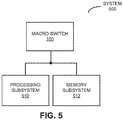
- Macro-switch 100 may be included in a system and/or an electronic device. This is shown in FIG. 5 , which presents a block diagram illustrating a system 500 that includes macro-switch 100.
- system 500 includes processing subsystem 510 (with one or more processors) and memory subsystem 512 (with memory).
- system 500 may include one or more program modules or sets of instructions stored in a memory subsystem 512 (such as DRAM or another type of volatile or non-volatile computer-readable memory), which, during operation, may be executed by processing subsystem 510.
- a memory subsystem 512 such as DRAM or another type of volatile or non-volatile computer-readable memory
- the one or more computer programs may constitute a computer-program mechanism.
- instructions in the various modules in memory subsystem 512 may be implemented in: a high-level procedural language, an object-oriented programming language, and/or in an assembly or machine language.
- the programming language may be compiled or interpreted, e.g., configurable or configured, to be executed by the processing subsystem.
- Components in system 500 may be coupled by signal lines, links or buses. These connections may include electrical, optical, or electro-optical communication of signals and/or data. Furthermore, in the preceding embodiments, some components are shown directly connected to one another, while others are shown connected via intermediate components. In each instance, the method of interconnection, or 'coupling,' establishes some desired communication between two or more circuit nodes, or terminals. Such coupling may often be accomplished using a number of circuit configurations, as will be understood by those of skill in the art; for example, AC coupling and/or DC coupling may be used.
- functionality in these circuits, components and devices may be implemented in one or more: application-specific integrated circuits ( ASICs ) , field-programmable gate arrays ( FPGAs ) , and/or one or more digital signal processors ( DSPs ) .
- ASICs application-specific integrated circuits
- FPGAs field-programmable gate arrays
- DSPs digital signal processors
- functionality in the preceding embodiments may be implemented more in hardware and less in software, or less in hardware and more in software, as is known in the art.
- system 500 may be at one location or may be distributed over multiple, geographically dispersed locations.
- System 500 may include: a VLSI circuit, a switch, a hub, a bridge, a router, a communication system (such as a wavelength-division-multiplexing communication system), a storage area network, a data center, a network (such as a local area network), and/or a computer system (such as a multiple-core processor computer system).
- a VLSI circuit such as a switch, a hub, a bridge, a router, a communication system (such as a wavelength-division-multiplexing communication system), a storage area network, a data center, a network (such as a local area network), and/or a computer system (such as a multiple-core processor computer system).
- the computer system may include, but is not limited to: a server (such as a multi-socket, multi-rack server), a laptop computer, a communication device or system, a personal computer, a work station, a mainframe computer, a blade, an enterprise computer, a data center, a tablet computer, a supercomputer, a network-attached-storage (NAS ) system, a storage-area-network (SAN ) system, a media player (such as an MP3 player), an appliance, a subnotebook/netbook, a tablet computer, a smartphone, a cellular telephone, a network appliance, a set-top box, a personal digital assistant ( PDA ) , a toy, a controller, a digital signal processor, a game console, a device controller, a computational engine within an appliance, a consumer-electronic device, a portable computing device or a portable electronic device, a personal organizer, and/or another electronic device.
- a server such as a multi-
- the embodiments of macro-switch 100 and/or system 500 may include fewer components or additional components. Although these embodiments are illustrated as having a number of discrete items, these optical components, integrated circuits and the system are intended to be functional descriptions of the various features that may be present rather than structural schematics of the embodiments described herein. Consequently, in these embodiments two or more components may be combined into a single component, and/or a position of one or more components may be changed. In addition, functionality in the preceding embodiments of macro-switch 100 and/or system 500 may be implemented more in hardware and less in software, or less in hardware and more in software, as is known in the art.
- the preceding embodiments have been illustrated with particular elements and compounds, a wide variety of materials and compositions (including stoichiometric and non-stoichiometric compositions) may be used, as is known to one of skill in the art.
- a silicon optical waveguide was illustrated in the preceding embodiments, the switching technique may be used with other materials, as is known to one of skill in the art.
- the semiconductor layer may include polysilicon or amorphous silicon.
- the materials and compounds in the macro-switch may be fabricated using a wide variety of processing techniques, including: evaporation, sputtering, molecular-beam epitaxy, chemical vapor deposition, wet or dry etching (such as photolithography or direct-write lithography), polishing, etc.
- components in macro-switch 100 may be defined using an additive process (i.e., material deposition) and/or a subtractive process (i.e., material removal), and these components may be fabricated using a wide variety of materials, including: a semiconductor, metal, glass, sapphire, silicon dioxide, organic materials, inorganic materials, a resin and/or polymers.
- a wide variety of optical components may be used in or in conjunction with macro-switch 100.
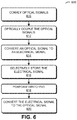
- FIG. 6 presents a flow chart illustrating a method 600 for switching optical signals using a macro-switch, such as macro-switch 100 ( FIGs. 1 and 2 ).
- the macro-switch conveys the optical signals (operation 610) in optical waveguides in a second integrated circuit in the macro-switch.
- the macro-switch optically couples the optical signals (operation 612) from the optical waveguide to and from switch sites in a first integrated circuit in the macro-switch, where a given switch site includes control logic and a memory buffer, and where the control logic determines a switching schedule independently of other switch sites in the macro- switch.
- the macro-switch converts an optical signal to an electrical signal (operation 614), performs switching (operation 618), and converts the electrical signal into the optical signal (operation 620), where the electrical signal is selectively stored (operation 616) in the memory buffer to avoid contention in the macro-switch.
- method 600 there may be additional or fewer operations. Moreover, the order of the operations may be changed, and/or two or more operations may be combined into a single operation.
Landscapes
- Engineering & Computer Science (AREA)
- Computer Networks & Wireless Communication (AREA)
- Physics & Mathematics (AREA)
- Signal Processing (AREA)
- General Physics & Mathematics (AREA)
- Optics & Photonics (AREA)
- Electromagnetism (AREA)
- Optical Communication System (AREA)
- Optical Modulation, Optical Deflection, Nonlinear Optics, Optical Demodulation, Optical Logic Elements (AREA)
- Optical Integrated Circuits (AREA)
- Use Of Switch Circuits For Exchanges And Methods Of Control Of Multiplex Exchanges (AREA)
Claims (13)
- Macrocommutateur optique (100), comprenant :un premier circuit intégré (110) ayant une surface (210), le premier circuit intégré comprenant :des premiers sites de commutation (114-1, 114-2, 114-N), chacun des premiers sites de commutation comportant une première logique de commande (116-1, 116-2, 116-N) et un premier tampon de mémoire (118-1, 118-2, 118-N) ; etdes deuxièmes sites de commutation (120-1, 1204-2, 1204-M), chacun des deuxièmes sites de commutation comportant une deuxième logique de commande (122-1, 122-2, 122-M) et un deuxième tampon de mémoire (124-1, 124-2, 124-M) ; etun deuxième circuit intégré (112) ayant une deuxième surface (212) en face de la surface, le deuxième circuit intégré comprenant :des ports optiques (130-1, 130-2, 130-3, 130-L) configurés pour se coupler à des sources optiques ;des premiers guides d'ondes optiques (126) optiquement couplés aux ports optiques et aux premiers sites de commutation ; etdes deuxièmes guides d'ondes optiques (128) optiquement couplés aux premiers sites de commutation et aux deuxièmes sites de commutation, le macrocommutateur ayant une topologie entièrement connectée entre les premiers sites de commutation et les deuxièmes sites de commutation.
- Macrocommutateur de la revendication 1, le macrocommutateur comportant un commutateur à point de croisement.
- Macrocommutateur de la revendication 1 ou 2, le macrocommutateur n'étant pas bloquant.
- Macrocommutateur d'une quelconque revendication précédente dans lequel, en fonctionnement, la première logique de commande à un premier site de commutation donné détermine un premier calendrier de commutation donné pour le premier site de commutation donné ; et
dans lequel, en fonctionnement, la deuxième logique de commande à un deuxième site de commutation donné détermine un deuxième calendrier de commutation donné pour le deuxième site de commutation donné. - Macrocommutateur de la revendication 4, dans lequel le premier calendrier de commutation donné est déterminé indépendamment d'autres calendriers de commutation pour les premiers sites de commutation et les deuxièmes sites de commutation ; et
dans lequel le deuxième calendrier de commutation donné est déterminé indépendamment des autres calendriers de commutation pour les premiers sites de commutation et les deuxièmes sites de commutation. - Macrocommutateur d'une quelconque revendication précédente, dans lequel les premiers guides d'ondes optiques entre un port optique donné et un premier site de commutation donné comportent un guide d'ondes optiques qui, en fonctionnement, achemine des informations du port optique donné au premier site de commutation donné, et un autre guide d'ondes optiques qui, en fonctionnement, achemine des informations du premier site de commutation donné au port optique donné.
- Macrocommutateur d'une quelconque revendication précédente, dans lequel les deuxièmes guides d'ondes optiques entre un premier site de commutation donné et un deuxième site de commutation donné comportent un guide d'ondes optiques qui, en fonctionnement, achemine des informations du premier site de commutation donné au deuxième site de commutation donné, et un autre guide d'ondes optiques qui, en fonctionnement, achemine des informations du deuxième site de commutation donné au premier site de commutation donné.
- Macrocommutateur d'une quelconque revendication précédente, dans lequel le couplage optique implique un élément parmi : un réseau de diffraction, un miroir, une communication par proximité optique.
- Macrocommutateur d'une quelconque revendication précédente, dans lequel un premier site de commutation donné comporte des émetteurs-récepteurs qui, en fonctionnement, convertissent des signaux optiques d'entrée en signaux électriques d'entrée et des signaux électriques de sortie en signaux optiques de sortie ; et
dans lequel un deuxième site de commutation donné comporte des émetteurs-récepteurs qui, en fonctionnement, convertissent des deuxièmes signaux optiques d'entrée en deuxièmes signaux électriques d'entrée et des deuxièmes signaux électriques de sortie en deuxièmes signaux optiques de sortie. - Macrocommutateur d'une quelconque revendication précédente, dans lequel le deuxième circuit intégré comprend :un substrat ;une couche d'oxyde enterrée (BOX) disposée sur le substrat ; etune couche semi-conductrice disposée sur la couche BOX, les premiers guides d'ondes optiques et les deuxièmes guides d'ondes optiques étant, au moins en partie, mis en œuvre dans la couche semi-conductrice.
- Macrocommutateur de la revendication 10, dans lequel le substrat, la couche BOX et la couche semi-conductrice constituent une technologie de silicium sur isolant.
- Système (500), comprenant :un processeur (510) ;une mémoire (512), couplée au processeur, qui stocke un module de programme qui, en fonctionnement, est exécuté par le processeur ; etle macrocommutateur optique (100) d'une quelconque revendication précédente.
- Procédé (600) de commutation de signaux optiques utilisant le macrocommutateur optique des revendications 1 à 11, le procédé comprenant :l'acheminement (610) de signaux optiques dans des guides d'ondes optiques dans un deuxième circuit intégré dans le macrocommutateur ;le couplage optique (612) des signaux optiques provenant des guides d'ondes optiques vers et depuis des sites de commutation dans un premier circuit intégré dans le macrocommutateur, un site de commutation donné comportant une logique de commande et un tampon de mémoire, et la logique de commande déterminant un calendrier de commutation indépendamment d'autres sites de commutation dans le macrocommutateur ; etau site de commutation donné, la conversion (614) d'un signal optique en un signal électrique, la réalisation d'une commutation (618), et la conversion (620) du signal électrique en le signal optique, le signal électrique étant sélectivement stocké (616) dans le tampon de mémoire pour éviter un conflit dans le macrocommutateur.
Applications Claiming Priority (3)
| Application Number | Priority Date | Filing Date | Title |
|---|---|---|---|
| US201562173190P | 2015-06-09 | 2015-06-09 | |
| US15/154,619 US9693124B2 (en) | 2015-06-09 | 2016-05-13 | Macro-switch with a buffered switching matrix |
| PCT/US2016/036249 WO2016200831A1 (fr) | 2015-06-09 | 2016-06-07 | Macro-commutateur ayant une matrice de commutation à mémoire tampon |
Publications (2)
| Publication Number | Publication Date |
|---|---|
| EP3308484A1 EP3308484A1 (fr) | 2018-04-18 |
| EP3308484B1 true EP3308484B1 (fr) | 2020-10-28 |
Family
ID=56345197
Family Applications (1)
| Application Number | Title | Priority Date | Filing Date |
|---|---|---|---|
| EP16734775.6A Active EP3308484B1 (fr) | 2015-06-09 | 2016-06-07 | Macro-commutateur ayant une matrice de commutation à mémoire tampon |
Country Status (5)
| Country | Link |
|---|---|
| US (1) | US9693124B2 (fr) |
| EP (1) | EP3308484B1 (fr) |
| JP (1) | JP6683734B2 (fr) |
| CN (1) | CN107667537B (fr) |
| WO (1) | WO2016200831A1 (fr) |
Families Citing this family (15)
| Publication number | Priority date | Publication date | Assignee | Title |
|---|---|---|---|---|
| US20160380886A1 (en) * | 2015-06-25 | 2016-12-29 | Ciena Corporation | Distributed data center architecture |
| US11153164B2 (en) * | 2017-01-04 | 2021-10-19 | International Business Machines Corporation | Live, in-line hardware component upgrades in disaggregated systems |
| US10534598B2 (en) | 2017-01-04 | 2020-01-14 | International Business Machines Corporation | Rolling upgrades in disaggregated systems |
| GB2566248B (en) * | 2017-02-22 | 2020-01-01 | Rockley Photonics Ltd | Optoelectronic Switch |
| CN108199977A (zh) * | 2017-12-29 | 2018-06-22 | 国网湖南省电力有限公司 | 一种双活数据中心的多跳路由和调度方法 |
| US10938751B2 (en) | 2018-04-18 | 2021-03-02 | Hewlett Packard Enterprise Development Lp | Hierarchical switching devices |
| US10284291B1 (en) * | 2018-04-25 | 2019-05-07 | Western Digital Technologies, Inc. | Node configuration in optical network |
| US10757038B2 (en) | 2018-07-06 | 2020-08-25 | Hewlett Packard Enterprise Development Lp | Reservation-based switching devices |
| US10484763B1 (en) * | 2018-07-20 | 2019-11-19 | Hewlett Packard Enterprise Development Lp | Optical inter-switch link cluster |
| US11855913B2 (en) | 2018-10-31 | 2023-12-26 | Hewlett Packard Enterprise Development Lp | Hierarchical switching device with deadlockable storage and storage partitions |
| US11503387B2 (en) | 2020-05-21 | 2022-11-15 | Hewlett Packard Enterprise Development Lp | Zero added latency packet reroute via silicon photonics |
| US11490177B1 (en) * | 2020-06-05 | 2022-11-01 | Luminous Computing, Inc. | Optical link system and method for computation |
| US11340410B2 (en) | 2020-10-19 | 2022-05-24 | Hewlett Packard Enterprise Development Lp | Dimensionally all-to-all connected network system using photonic crossbars and quad-node-loop routing |
| US11323787B1 (en) | 2020-10-30 | 2022-05-03 | Hewlett Packard Enterprise Development Lp | Multi-chip photonic node for scalable all-to-all connected fabrics |
| US11609375B2 (en) | 2021-02-22 | 2023-03-21 | Luminous Computing, Inc. | Photonic integrated circuit system and method of fabrication |
Family Cites Families (14)
| Publication number | Priority date | Publication date | Assignee | Title |
|---|---|---|---|---|
| JP3634992B2 (ja) * | 1999-11-04 | 2005-03-30 | 日本電信電話株式会社 | 可変長パケットスイッチ |
| JP2005150776A (ja) * | 2003-11-11 | 2005-06-09 | Hitachi Ltd | パケット交換装置 |
| WO2006129789A1 (fr) * | 2005-06-02 | 2006-12-07 | Nec Corporation | Dispositif et procede de commutation, et programme de controle de commutation |
| US7356213B1 (en) * | 2006-03-28 | 2008-04-08 | Sun Microsystems, Inc. | Transparent switch using optical and electrical proximity communication |
| JP5012232B2 (ja) | 2007-06-08 | 2012-08-29 | 富士通株式会社 | 光スイッチ装置 |
| US8098968B2 (en) * | 2007-09-04 | 2012-01-17 | International Business Machines Corporation | Silicide thermal heaters for silicon-on-insulator nanophotonic devices |
| US8938139B2 (en) * | 2008-03-11 | 2015-01-20 | Hewlett-Packard Development Company, L.P. | Optoelectronic switches using on-chip optical waveguides |
| US8265433B2 (en) * | 2010-04-14 | 2012-09-11 | Oracle America, Inc. | Low-power, broadband optical switch |
| US8399292B2 (en) * | 2010-06-30 | 2013-03-19 | International Business Machines Corporation | Fabricating a semiconductor chip with backside optical vias |
| US9008510B1 (en) * | 2011-05-12 | 2015-04-14 | Google Inc. | Implementation of a large-scale multi-stage non-blocking optical circuit switch |
| US9300398B2 (en) * | 2012-01-09 | 2016-03-29 | Attochron, Llc | USPL-FSO lasercom point-to-point and point-to-multipoint optical wireless communication |
| US8983293B2 (en) * | 2012-04-25 | 2015-03-17 | Ciena Corporation | Electro-optical switching fabric systems and methods |
| US9065722B2 (en) * | 2012-12-23 | 2015-06-23 | Advanced Micro Devices, Inc. | Die-stacked device with partitioned multi-hop network |
| US8988770B2 (en) | 2013-03-14 | 2015-03-24 | Oracle International Corporation | Hybrid optical source with semiconductor reflector |
-
2016
- 2016-05-13 US US15/154,619 patent/US9693124B2/en active Active
- 2016-06-07 WO PCT/US2016/036249 patent/WO2016200831A1/fr unknown
- 2016-06-07 JP JP2017558422A patent/JP6683734B2/ja active Active
- 2016-06-07 CN CN201680030884.2A patent/CN107667537B/zh active Active
- 2016-06-07 EP EP16734775.6A patent/EP3308484B1/fr active Active
Non-Patent Citations (1)
| Title |
|---|
| None * |
Also Published As
| Publication number | Publication date |
|---|---|
| US20160366498A1 (en) | 2016-12-15 |
| JP2018527767A (ja) | 2018-09-20 |
| CN107667537A (zh) | 2018-02-06 |
| CN107667537B (zh) | 2020-05-19 |
| EP3308484A1 (fr) | 2018-04-18 |
| US9693124B2 (en) | 2017-06-27 |
| WO2016200831A1 (fr) | 2016-12-15 |
| JP6683734B2 (ja) | 2020-04-22 |
Similar Documents
| Publication | Publication Date | Title |
|---|---|---|
| EP3308484B1 (fr) | Macro-commutateur ayant une matrice de commutation à mémoire tampon | |
| US20230231799A1 (en) | Data center network with packet spraying | |
| US11469922B2 (en) | Data center network with multiplexed communication of data packets across servers | |
| Xi et al. | A petabit bufferless optical switch for data center networks | |
| Schares et al. | Optics in future data center networks | |
| Liu et al. | Low latency optical switch for high performance computing with minimized processor energy load | |
| CN105917663B (zh) | 光交换机架构 | |
| Maniotis et al. | Intra-node high-performance computing network architecture with nanosecond-scale photonic switches | |
| Siokis et al. | Electro-optic switches based on space switching of multiplexed WDM signals: blocking vs non-blocking design trade-offs | |
| US20230308787A1 (en) | Hybrid optoelectrical switches | |
| US11800266B2 (en) | Hybrid optoelectrical switches | |
| Sinha et al. | Comparative analysis of optical data center switches | |
| Moralis-Pegios et al. | A low-latency high-port count optical switch with optical delay line buffering for disaggregated data centers | |
| Szymanski | Impact of future trends on exascale grid and cloud computing | |
| Wang et al. | HERO: Pbit high-radix optical switch based on integrated silicon photonics for data center | |
| Patronas et al. | Switching functions of a data center Top-of-Rack (ToR) | |
| CN115378886B (zh) | 混合光电交换机 | |
| Yin et al. | Experimental demonstration of LIONS: A low latency optical switch for high performance computing | |
| Yu et al. | MPNACK: an optical switching scheme enabling the buffer-less reliable transmission | |
| Liu et al. | A low latency optical top of rack switch for data centre networks with minimized processor energy load | |
| CN115378886A (zh) | 混合光电交换机 | |
| US11310115B2 (en) | TClos—scalable network topology and system architecture | |
| Maniotis et al. | Intra-node high-performance computing network architecture with fast optical switch fabrics | |
| EP4020848A1 (fr) | Conversion de plusieurs signaux lumineux dans et à partir d'une seule longueur onde avec plusieurs polarisations pour augmenter la largeur de bande optique | |
| Kitayama et al. | Energy-efficient, high-performance optoelectronic packet switching for intra-data center network |
Legal Events
| Date | Code | Title | Description |
|---|---|---|---|
| STAA | Information on the status of an ep patent application or granted ep patent |
Free format text: STATUS: THE INTERNATIONAL PUBLICATION HAS BEEN MADE |
|
| PUAI | Public reference made under article 153(3) epc to a published international application that has entered the european phase |
Free format text: ORIGINAL CODE: 0009012 |
|
| STAA | Information on the status of an ep patent application or granted ep patent |
Free format text: STATUS: REQUEST FOR EXAMINATION WAS MADE |
|
| 17P | Request for examination filed |
Effective date: 20171209 |
|
| AK | Designated contracting states |
Kind code of ref document: A1 Designated state(s): AL AT BE BG CH CY CZ DE DK EE ES FI FR GB GR HR HU IE IS IT LI LT LU LV MC MK MT NL NO PL PT RO RS SE SI SK SM TR |
|
| AX | Request for extension of the european patent |
Extension state: BA ME |
|
| DAV | Request for validation of the european patent (deleted) | ||
| DAX | Request for extension of the european patent (deleted) | ||
| STAA | Information on the status of an ep patent application or granted ep patent |
Free format text: STATUS: EXAMINATION IS IN PROGRESS |
|
| 17Q | First examination report despatched |
Effective date: 20190325 |
|
| GRAP | Despatch of communication of intention to grant a patent |
Free format text: ORIGINAL CODE: EPIDOSNIGR1 |
|
| STAA | Information on the status of an ep patent application or granted ep patent |
Free format text: STATUS: GRANT OF PATENT IS INTENDED |
|
| INTG | Intention to grant announced |
Effective date: 20200605 |
|
| GRAS | Grant fee paid |
Free format text: ORIGINAL CODE: EPIDOSNIGR3 |
|
| GRAA | (expected) grant |
Free format text: ORIGINAL CODE: 0009210 |
|
| STAA | Information on the status of an ep patent application or granted ep patent |
Free format text: STATUS: THE PATENT HAS BEEN GRANTED |
|
| AK | Designated contracting states |
Kind code of ref document: B1 Designated state(s): AL AT BE BG CH CY CZ DE DK EE ES FI FR GB GR HR HU IE IS IT LI LT LU LV MC MK MT NL NO PL PT RO RS SE SI SK SM TR |
|
| REG | Reference to a national code |
Ref country code: GB Ref legal event code: FG4D |
|
| REG | Reference to a national code |
Ref country code: CH Ref legal event code: EP |
|
| REG | Reference to a national code |
Ref country code: AT Ref legal event code: REF Ref document number: 1329311 Country of ref document: AT Kind code of ref document: T Effective date: 20201115 |
|
| REG | Reference to a national code |
Ref country code: DE Ref legal event code: R096 Ref document number: 602016046693 Country of ref document: DE |
|
| REG | Reference to a national code |
Ref country code: IE Ref legal event code: FG4D |
|
| REG | Reference to a national code |
Ref country code: AT Ref legal event code: MK05 Ref document number: 1329311 Country of ref document: AT Kind code of ref document: T Effective date: 20201028 |
|
| REG | Reference to a national code |
Ref country code: NL Ref legal event code: MP Effective date: 20201028 |
|
| PG25 | Lapsed in a contracting state [announced via postgrant information from national office to epo] |
Ref country code: GR Free format text: LAPSE BECAUSE OF FAILURE TO SUBMIT A TRANSLATION OF THE DESCRIPTION OR TO PAY THE FEE WITHIN THE PRESCRIBED TIME-LIMIT Effective date: 20210129 Ref country code: FI Free format text: LAPSE BECAUSE OF FAILURE TO SUBMIT A TRANSLATION OF THE DESCRIPTION OR TO PAY THE FEE WITHIN THE PRESCRIBED TIME-LIMIT Effective date: 20201028 Ref country code: RS Free format text: LAPSE BECAUSE OF FAILURE TO SUBMIT A TRANSLATION OF THE DESCRIPTION OR TO PAY THE FEE WITHIN THE PRESCRIBED TIME-LIMIT Effective date: 20201028 Ref country code: PT Free format text: LAPSE BECAUSE OF FAILURE TO SUBMIT A TRANSLATION OF THE DESCRIPTION OR TO PAY THE FEE WITHIN THE PRESCRIBED TIME-LIMIT Effective date: 20210301 Ref country code: NO Free format text: LAPSE BECAUSE OF FAILURE TO SUBMIT A TRANSLATION OF THE DESCRIPTION OR TO PAY THE FEE WITHIN THE PRESCRIBED TIME-LIMIT Effective date: 20210128 |
|
| REG | Reference to a national code |
Ref country code: LT Ref legal event code: MG4D |
|
| PG25 | Lapsed in a contracting state [announced via postgrant information from national office to epo] |
Ref country code: AT Free format text: LAPSE BECAUSE OF FAILURE TO SUBMIT A TRANSLATION OF THE DESCRIPTION OR TO PAY THE FEE WITHIN THE PRESCRIBED TIME-LIMIT Effective date: 20201028 Ref country code: ES Free format text: LAPSE BECAUSE OF FAILURE TO SUBMIT A TRANSLATION OF THE DESCRIPTION OR TO PAY THE FEE WITHIN THE PRESCRIBED TIME-LIMIT Effective date: 20201028 Ref country code: PL Free format text: LAPSE BECAUSE OF FAILURE TO SUBMIT A TRANSLATION OF THE DESCRIPTION OR TO PAY THE FEE WITHIN THE PRESCRIBED TIME-LIMIT Effective date: 20201028 Ref country code: LV Free format text: LAPSE BECAUSE OF FAILURE TO SUBMIT A TRANSLATION OF THE DESCRIPTION OR TO PAY THE FEE WITHIN THE PRESCRIBED TIME-LIMIT Effective date: 20201028 Ref country code: IS Free format text: LAPSE BECAUSE OF FAILURE TO SUBMIT A TRANSLATION OF THE DESCRIPTION OR TO PAY THE FEE WITHIN THE PRESCRIBED TIME-LIMIT Effective date: 20210228 Ref country code: BG Free format text: LAPSE BECAUSE OF FAILURE TO SUBMIT A TRANSLATION OF THE DESCRIPTION OR TO PAY THE FEE WITHIN THE PRESCRIBED TIME-LIMIT Effective date: 20210128 Ref country code: SE Free format text: LAPSE BECAUSE OF FAILURE TO SUBMIT A TRANSLATION OF THE DESCRIPTION OR TO PAY THE FEE WITHIN THE PRESCRIBED TIME-LIMIT Effective date: 20201028 |
|
| PG25 | Lapsed in a contracting state [announced via postgrant information from national office to epo] |
Ref country code: HR Free format text: LAPSE BECAUSE OF FAILURE TO SUBMIT A TRANSLATION OF THE DESCRIPTION OR TO PAY THE FEE WITHIN THE PRESCRIBED TIME-LIMIT Effective date: 20201028 Ref country code: NL Free format text: LAPSE BECAUSE OF FAILURE TO SUBMIT A TRANSLATION OF THE DESCRIPTION OR TO PAY THE FEE WITHIN THE PRESCRIBED TIME-LIMIT Effective date: 20201028 |
|
| REG | Reference to a national code |
Ref country code: DE Ref legal event code: R097 Ref document number: 602016046693 Country of ref document: DE |
|
| PG25 | Lapsed in a contracting state [announced via postgrant information from national office to epo] |
Ref country code: SK Free format text: LAPSE BECAUSE OF FAILURE TO SUBMIT A TRANSLATION OF THE DESCRIPTION OR TO PAY THE FEE WITHIN THE PRESCRIBED TIME-LIMIT Effective date: 20201028 Ref country code: RO Free format text: LAPSE BECAUSE OF FAILURE TO SUBMIT A TRANSLATION OF THE DESCRIPTION OR TO PAY THE FEE WITHIN THE PRESCRIBED TIME-LIMIT Effective date: 20201028 Ref country code: CZ Free format text: LAPSE BECAUSE OF FAILURE TO SUBMIT A TRANSLATION OF THE DESCRIPTION OR TO PAY THE FEE WITHIN THE PRESCRIBED TIME-LIMIT Effective date: 20201028 Ref country code: EE Free format text: LAPSE BECAUSE OF FAILURE TO SUBMIT A TRANSLATION OF THE DESCRIPTION OR TO PAY THE FEE WITHIN THE PRESCRIBED TIME-LIMIT Effective date: 20201028 Ref country code: SM Free format text: LAPSE BECAUSE OF FAILURE TO SUBMIT A TRANSLATION OF THE DESCRIPTION OR TO PAY THE FEE WITHIN THE PRESCRIBED TIME-LIMIT Effective date: 20201028 Ref country code: LT Free format text: LAPSE BECAUSE OF FAILURE TO SUBMIT A TRANSLATION OF THE DESCRIPTION OR TO PAY THE FEE WITHIN THE PRESCRIBED TIME-LIMIT Effective date: 20201028 |
|
| PG25 | Lapsed in a contracting state [announced via postgrant information from national office to epo] |
Ref country code: DK Free format text: LAPSE BECAUSE OF FAILURE TO SUBMIT A TRANSLATION OF THE DESCRIPTION OR TO PAY THE FEE WITHIN THE PRESCRIBED TIME-LIMIT Effective date: 20201028 |
|
| PLBE | No opposition filed within time limit |
Free format text: ORIGINAL CODE: 0009261 |
|
| STAA | Information on the status of an ep patent application or granted ep patent |
Free format text: STATUS: NO OPPOSITION FILED WITHIN TIME LIMIT |
|
| 26N | No opposition filed |
Effective date: 20210729 |
|
| PG25 | Lapsed in a contracting state [announced via postgrant information from national office to epo] |
Ref country code: AL Free format text: LAPSE BECAUSE OF FAILURE TO SUBMIT A TRANSLATION OF THE DESCRIPTION OR TO PAY THE FEE WITHIN THE PRESCRIBED TIME-LIMIT Effective date: 20201028 Ref country code: IT Free format text: LAPSE BECAUSE OF FAILURE TO SUBMIT A TRANSLATION OF THE DESCRIPTION OR TO PAY THE FEE WITHIN THE PRESCRIBED TIME-LIMIT Effective date: 20201028 |
|
| PG25 | Lapsed in a contracting state [announced via postgrant information from national office to epo] |
Ref country code: SI Free format text: LAPSE BECAUSE OF FAILURE TO SUBMIT A TRANSLATION OF THE DESCRIPTION OR TO PAY THE FEE WITHIN THE PRESCRIBED TIME-LIMIT Effective date: 20201028 |
|
| PG25 | Lapsed in a contracting state [announced via postgrant information from national office to epo] |
Ref country code: MC Free format text: LAPSE BECAUSE OF FAILURE TO SUBMIT A TRANSLATION OF THE DESCRIPTION OR TO PAY THE FEE WITHIN THE PRESCRIBED TIME-LIMIT Effective date: 20201028 |
|
| REG | Reference to a national code |
Ref country code: CH Ref legal event code: PL |
|
| REG | Reference to a national code |
Ref country code: BE Ref legal event code: MM Effective date: 20210630 |
|
| PG25 | Lapsed in a contracting state [announced via postgrant information from national office to epo] |
Ref country code: LU Free format text: LAPSE BECAUSE OF NON-PAYMENT OF DUE FEES Effective date: 20210607 |
|
| PG25 | Lapsed in a contracting state [announced via postgrant information from national office to epo] |
Ref country code: LI Free format text: LAPSE BECAUSE OF NON-PAYMENT OF DUE FEES Effective date: 20210630 Ref country code: IE Free format text: LAPSE BECAUSE OF NON-PAYMENT OF DUE FEES Effective date: 20210607 Ref country code: CH Free format text: LAPSE BECAUSE OF NON-PAYMENT OF DUE FEES Effective date: 20210630 |
|
| PG25 | Lapsed in a contracting state [announced via postgrant information from national office to epo] |
Ref country code: IS Free format text: LAPSE BECAUSE OF FAILURE TO SUBMIT A TRANSLATION OF THE DESCRIPTION OR TO PAY THE FEE WITHIN THE PRESCRIBED TIME-LIMIT Effective date: 20210228 Ref country code: FR Free format text: LAPSE BECAUSE OF NON-PAYMENT OF DUE FEES Effective date: 20210630 |
|
| PG25 | Lapsed in a contracting state [announced via postgrant information from national office to epo] |
Ref country code: BE Free format text: LAPSE BECAUSE OF NON-PAYMENT OF DUE FEES Effective date: 20210630 |
|
| P01 | Opt-out of the competence of the unified patent court (upc) registered |
Effective date: 20230522 |
|
| PG25 | Lapsed in a contracting state [announced via postgrant information from national office to epo] |
Ref country code: CY Free format text: LAPSE BECAUSE OF FAILURE TO SUBMIT A TRANSLATION OF THE DESCRIPTION OR TO PAY THE FEE WITHIN THE PRESCRIBED TIME-LIMIT Effective date: 20201028 |
|
| PG25 | Lapsed in a contracting state [announced via postgrant information from national office to epo] |
Ref country code: HU Free format text: LAPSE BECAUSE OF FAILURE TO SUBMIT A TRANSLATION OF THE DESCRIPTION OR TO PAY THE FEE WITHIN THE PRESCRIBED TIME-LIMIT; INVALID AB INITIO Effective date: 20160607 |
|
| PGFP | Annual fee paid to national office [announced via postgrant information from national office to epo] |
Ref country code: DE Payment date: 20230502 Year of fee payment: 8 |
|
| PGFP | Annual fee paid to national office [announced via postgrant information from national office to epo] |
Ref country code: GB Payment date: 20230504 Year of fee payment: 8 |
|
| PG25 | Lapsed in a contracting state [announced via postgrant information from national office to epo] |
Ref country code: MK Free format text: LAPSE BECAUSE OF FAILURE TO SUBMIT A TRANSLATION OF THE DESCRIPTION OR TO PAY THE FEE WITHIN THE PRESCRIBED TIME-LIMIT Effective date: 20201028 |