EP3308464B1 - High efficiency half-cross-coupled decoupling capacitor - Google Patents
High efficiency half-cross-coupled decoupling capacitor Download PDFInfo
- Publication number
- EP3308464B1 EP3308464B1 EP15895123.6A EP15895123A EP3308464B1 EP 3308464 B1 EP3308464 B1 EP 3308464B1 EP 15895123 A EP15895123 A EP 15895123A EP 3308464 B1 EP3308464 B1 EP 3308464B1
- Authority
- EP
- European Patent Office
- Prior art keywords
- nfet
- pfet
- gate
- drain
- source
- Prior art date
- Legal status (The legal status is an assumption and is not a legal conclusion. Google has not performed a legal analysis and makes no representation as to the accuracy of the status listed.)
- Active
Links
- 239000003990 capacitor Substances 0.000 title description 17
- 230000005669 field effect Effects 0.000 claims description 17
- 238000000034 method Methods 0.000 claims description 17
- 238000010586 diagram Methods 0.000 description 26
- 230000004044 response Effects 0.000 description 5
- 238000004519 manufacturing process Methods 0.000 description 3
- 230000001629 suppression Effects 0.000 description 3
- 208000032750 Device leakage Diseases 0.000 description 2
- 230000008569 process Effects 0.000 description 2
- 230000007423 decrease Effects 0.000 description 1
- 230000003993 interaction Effects 0.000 description 1
- 239000000463 material Substances 0.000 description 1
- 239000002184 metal Substances 0.000 description 1
- 229910021420 polycrystalline silicon Inorganic materials 0.000 description 1
- 239000007787 solid Substances 0.000 description 1
- 239000006163 transport media Substances 0.000 description 1
- 235000001892 vitamin D2 Nutrition 0.000 description 1
Images


Classifications
-
- H—ELECTRICITY
- H01—ELECTRIC ELEMENTS
- H01L—SEMICONDUCTOR DEVICES NOT COVERED BY CLASS H10
- H01L27/00—Devices consisting of a plurality of semiconductor or other solid-state components formed in or on a common substrate
- H01L27/02—Devices consisting of a plurality of semiconductor or other solid-state components formed in or on a common substrate including semiconductor components specially adapted for rectifying, oscillating, amplifying or switching and having at least one potential-jump barrier or surface barrier; including integrated passive circuit elements with at least one potential-jump barrier or surface barrier
- H01L27/0203—Particular design considerations for integrated circuits
- H01L27/0248—Particular design considerations for integrated circuits for electrical or thermal protection, e.g. electrostatic discharge [ESD] protection
-
- H—ELECTRICITY
- H01—ELECTRIC ELEMENTS
- H01L—SEMICONDUCTOR DEVICES NOT COVERED BY CLASS H10
- H01L27/00—Devices consisting of a plurality of semiconductor or other solid-state components formed in or on a common substrate
- H01L27/02—Devices consisting of a plurality of semiconductor or other solid-state components formed in or on a common substrate including semiconductor components specially adapted for rectifying, oscillating, amplifying or switching and having at least one potential-jump barrier or surface barrier; including integrated passive circuit elements with at least one potential-jump barrier or surface barrier
- H01L27/04—Devices consisting of a plurality of semiconductor or other solid-state components formed in or on a common substrate including semiconductor components specially adapted for rectifying, oscillating, amplifying or switching and having at least one potential-jump barrier or surface barrier; including integrated passive circuit elements with at least one potential-jump barrier or surface barrier the substrate being a semiconductor body
- H01L27/06—Devices consisting of a plurality of semiconductor or other solid-state components formed in or on a common substrate including semiconductor components specially adapted for rectifying, oscillating, amplifying or switching and having at least one potential-jump barrier or surface barrier; including integrated passive circuit elements with at least one potential-jump barrier or surface barrier the substrate being a semiconductor body including a plurality of individual components in a non-repetitive configuration
- H01L27/0611—Devices consisting of a plurality of semiconductor or other solid-state components formed in or on a common substrate including semiconductor components specially adapted for rectifying, oscillating, amplifying or switching and having at least one potential-jump barrier or surface barrier; including integrated passive circuit elements with at least one potential-jump barrier or surface barrier the substrate being a semiconductor body including a plurality of individual components in a non-repetitive configuration integrated circuits having a two-dimensional layout of components without a common active region
- H01L27/0617—Devices consisting of a plurality of semiconductor or other solid-state components formed in or on a common substrate including semiconductor components specially adapted for rectifying, oscillating, amplifying or switching and having at least one potential-jump barrier or surface barrier; including integrated passive circuit elements with at least one potential-jump barrier or surface barrier the substrate being a semiconductor body including a plurality of individual components in a non-repetitive configuration integrated circuits having a two-dimensional layout of components without a common active region comprising components of the field-effect type
- H01L27/0629—Devices consisting of a plurality of semiconductor or other solid-state components formed in or on a common substrate including semiconductor components specially adapted for rectifying, oscillating, amplifying or switching and having at least one potential-jump barrier or surface barrier; including integrated passive circuit elements with at least one potential-jump barrier or surface barrier the substrate being a semiconductor body including a plurality of individual components in a non-repetitive configuration integrated circuits having a two-dimensional layout of components without a common active region comprising components of the field-effect type in combination with diodes, or resistors, or capacitors
-
- H—ELECTRICITY
- H01—ELECTRIC ELEMENTS
- H01L—SEMICONDUCTOR DEVICES NOT COVERED BY CLASS H10
- H01L27/00—Devices consisting of a plurality of semiconductor or other solid-state components formed in or on a common substrate
- H01L27/02—Devices consisting of a plurality of semiconductor or other solid-state components formed in or on a common substrate including semiconductor components specially adapted for rectifying, oscillating, amplifying or switching and having at least one potential-jump barrier or surface barrier; including integrated passive circuit elements with at least one potential-jump barrier or surface barrier
- H01L27/04—Devices consisting of a plurality of semiconductor or other solid-state components formed in or on a common substrate including semiconductor components specially adapted for rectifying, oscillating, amplifying or switching and having at least one potential-jump barrier or surface barrier; including integrated passive circuit elements with at least one potential-jump barrier or surface barrier the substrate being a semiconductor body
- H01L27/08—Devices consisting of a plurality of semiconductor or other solid-state components formed in or on a common substrate including semiconductor components specially adapted for rectifying, oscillating, amplifying or switching and having at least one potential-jump barrier or surface barrier; including integrated passive circuit elements with at least one potential-jump barrier or surface barrier the substrate being a semiconductor body including only semiconductor components of a single kind
- H01L27/0805—Capacitors only
-
- H—ELECTRICITY
- H01—ELECTRIC ELEMENTS
- H01L—SEMICONDUCTOR DEVICES NOT COVERED BY CLASS H10
- H01L29/00—Semiconductor devices adapted for rectifying, amplifying, oscillating or switching, or capacitors or resistors with at least one potential-jump barrier or surface barrier, e.g. PN junction depletion layer or carrier concentration layer; Details of semiconductor bodies or of electrodes thereof ; Multistep manufacturing processes therefor
- H01L29/66—Types of semiconductor device ; Multistep manufacturing processes therefor
- H01L29/86—Types of semiconductor device ; Multistep manufacturing processes therefor controllable only by variation of the electric current supplied, or only the electric potential applied, to one or more of the electrodes carrying the current to be rectified, amplified, oscillated or switched
- H01L29/92—Capacitors with potential-jump barrier or surface barrier
- H01L29/94—Metal-insulator-semiconductors, e.g. MOS
Definitions
- This disclosure relates generally to a decoupling capacitor circuit design for suppressing supply noise that provides high operational frequency and high area efficiency.
- DCAPs Decoupling capacitors
- PDNs power distribution networks
- VLSI very-large-scale-integration
- DCAP design includes high area efficiency, robust electrical properties, and properly targeted operational frequency.
- some DCAP designs are susceptible to damage from electro-static discharge (ESD) events, particularly as the transistor designs enter into ultra-deep sub-micron and finFET process nodes.
- ESD electro-static discharge
- designs intended to render the DCAP more resistant to ESD damage are often hindered by an inherent trade-off between high area efficiency and high frequency operation.
- FET field-effect transistor
- each field-effect transistor (FET) that is used as a decoupling capacitor has its drain, source, and body coupled to a first power source voltage VDD or VSS, and its gate coupled to the other power source voltage.
- Another prior art solution is known from the document US 2007/230087 A1 , which considers using MOS transistors in decoupling capacitor structures.
- a first MOS transistor of the first conductivity type, functions as a resistor element due to an on-resistance between its source and drain.
- the source is connected to a first power supply wiring.
- a second MOS transistor, of the second conductivity type, is connected to the second power supply wiring and functions as a capacitor element and has a gate length greater than that of the first MOS transistor.
- a decoupling capacitor (DCAP) circuit that yields high operational frequency without sacrificing area efficiency.
- DCAP decoupling capacitor
- PFET p-channel field effect transistor
- HCC half-cross-coupled
- AEC area efficient capacitance
- the size of the HCC FETs can set the operating frequency of the circuit independently of the area efficiency, while the size of the AEC device(s) can set the area efficiency independently of the operating frequency.
- the DCAP design described herein eliminates the undesirable trade-off between operating frequency and area efficiency inherent in some conventional DCAP designs.
- the decoupling capacitor circuit may comprise a first p-channel field effect transistor (PFET); a first n-channel field effect transistor (NFET); and at least one capacitive device, wherein a first PFET source and a first PFET body of the first PFET are connected to a voltage supply, a first NFET source and a first NFET body of the first NFET are connected to ground, the at least one capacitive device is connected to at least one of a first PFET gate of the first PFET or a first NFET gate of the first NFET, and inclusion of the at least one capacitive device increases an area efficiency of the decoupling capacitor circuit without changing a frequency response of the decoupling capacitor circuit.
- PFET p-channel field effect transistor
- NFET n-channel field effect transistor
- a method for suppressing power supply noise comprising connecting a first source and a first body of a first p-channel field effect transistor (PFET) to a voltage supply; connecting a second source and a second body of an n-channel field effect transistor (NFET) to ground; connecting a first drain of the first PFET to a first gate of the NFET; connecting a second drain of the NFET to a second gate of the first PFET; connecting a third drain, a third source, and a third body of a second PFET to the voltage supply; and connecting a third gate of the second PFET to the second gate of the first PFET.
- PFET p-channel field effect transistor
- NFET n-channel field effect transistor
- a system for suppressing power supply noise may comprise a first p-channel field effect transistor (PFET), wherein a first PFET source and a first PFET body of the first PFET are connected to a voltage supply; a first n-channel field effect transistor (NFET), wherein a first NFET source and a first NFET body of the first NFET are connected to ground; and a second NFET, wherein a first PFET drain of the first PFET is connected to a first NFET gate of the first NFET, a first NFET drain of the first NFET is connected to a first PFET gate of the PFET, a second NFET drain, a second NFET source, and a second NFET body of the second NFET is connected to ground, and a second NFET gate of the second NFET is connected to the first NFET gate of the first NFET.
- PFET p-channel field effect transistor
- NFET n-channel field effect
- DCAPs are often used in power distribution networks of VLSI systems to suppress voltage supply noise or ripples induced by active circuit elements, thereby shielding other elements of the circuit from power supply voltage fluctuations that may damage the elements or impede their functions.
- Robust DCAP designs are characterized by high area efficiency, robust electrical properties, and properly targeted operational frequency.
- the targeted operational frequency ranges from the operating frequency to the switching slew of the gates in the design, thus constituting the high operational frequency of the DCAP used in the power distribution network.
- FIG. 1 is a circuit diagram illustrating one approach to DCAP design.
- the drain, source, and body of the p-channel field effect transistor (PFET) 102 is directly tied to the supply voltage 106, and the drain, source, and body of the n-channel field effect transistor (NFET) 104 is tied to ground.
- the gate 110 of the PFET 102 is tied to ground, and the gate 112 of the NFET 104 is tied to the supply voltage 106.
- This design can decouple supply noise to high operating frequencies while being area efficient.
- the transistor designs enter into ultra-deep sub-micron and finFET process nodes the gate oxides become exceedingly thin. Consequently, the design in FIG.
- ESD electro-static discharge
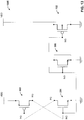
- FIG. 2 is a circuit diagram illustrating another DCAP design approach that attempts to address this issue by tying the source and body of the PFET 202 to the supply voltage 208 and the source and body of the NFET 204 to ground 206, while connecting the drain and gate nodes of the PFET and NFET in a half-cross-coupled (HCC) fashion. That is, the drain 210 of PFET 202 is connected to the gate 212 of NFET 204, while the drain 214 of NFET 204 is connected to the gate 216 of PFET 202.
- This design provides a resistive path from the supply voltage and ground nodes to the gate through device channels, thereby protecting the gate oxide during an ESD event until the ESD clamp can shunt the excess charge.
- a large channel for the design depicted in FIG. 2 will result in a high start-up time.
- This high start-up time is due to a "dead" zone in which the HCC nodes are brought up in states opposite to the values they require for the DCAP to function, and the design depends on the device leakage of the two FETS 202 and 204 to set the correct state values.
- a large channel will reduce this device leakage, resulting in a large increase in start-up time before the DCAP will be useful.
- FIG. 3 is a circuit diagram of an example DCAP circuit 300 not forming part of the claimed invention that provides high area efficiency and high frequency operation.
- This design includes a PFET 302 and an NFET 304 connected in an HCC configuration, and area efficient capacitance (AEC) devices 306 and 308 that serve as an area efficiency decoupling capacitor.
- the AEC devices 306 and 308 can comprise, for example, a second PFET and a second NFET, respectively. With AEC devices 306 and 308 in place, the HCC devices can be optimized to provide a high frequency response without being limited by the conflicting design requirements of high area efficiency.
- the drain, source, and body of PFET AEC device 306 are connected to the supply voltage 310, while the gate 312 is connected to the PG node produced by the HCC connections.
- the drain, source, and body of NFET AEC device 308 is connected to ground 314, while the gate 316 is connected to the NG node produced by the HCC connections.
- the circuit 300 depicted in FIG. 3 allows the device channel length of the HCC devices (PFET 302 and NFET 304) - and thus the corresponding resistance of the decoupling path through the PFET and NFET - to be kept low, thereby providing high frequency supply noise decoupling. Keeping the device channel length low also increases leakage in the HCC devices, thereby keeping start-up times low for scenarios in which the HCC connectivity is initialized to the incorrect states.
- the AEC devices 306 and 308 can be optimized to provide high area efficiency.
- the AEC devices 306 and 308 can be sized to provide high area efficiency without changing the channel length (and resistance) of the decoupling path through the PFET 302 and NFET 304, and thus without changing the operating frequency of the circuit 300.
- optimizing the AEC devices 306 and 308 for high area efficiency corresponds to having a large length (L).
- circuit 300 includes two AEC devices 306 and 308 corresponding to the PFET 302 and NFET 304, respectively, the embodiments of the present invention may include only one AEC device.
- FIG. 4 illustrates an embodiment in which only the PFET AEC device 306 is connected to the HCC circuit (omitting the NFET AEC device 308)
- FIG. 5 illustrates an embodiment in which only the NFET AEC device 308 is connected (omitting the PFET AEC device 306).
- FIG. 6 is a graph 602 illustrating the frequency response for circuit 300 for various sizes of AEC devices 306 and 308.
- Each plot of graph 602 represents the frequency response for a given size of AEC devices 306 and 308, with the sizes of the HCC devices 302 and 304 kept constant for each plot.
- the roll-off frequency ⁇ - that is, the frequency at which the capacitance of circuit 300 loses its effectiveness - is characterized by 1/(RC), where R is the resistance of the decoupling path determined by the size of the HCC devices 302 and 304, and C is the capacitance determined by the size of the AEC devices 306 and 308.
- the roll-off frequency ⁇ decreases.
- the HCC devices 302 and 304 can also be increased in order keep up with the increased capacitance of the AEC devices and thereby maintain high frequency supply noise decoupling.
- the ratio between the sizes of the HCC devices 302 and 304 to the capacitance on the AEC devices 306 and 308 determines the degree of high frequency operation.
- FIG. 7 is a circuit diagram of an example DCAP circuit 700 not forming part of the present invention that includes an AEC device 702 comprising a PFET having gate 704 tied to the NG node, source and drain tied to ground 314, and body tied to VDD 310.
- FIG. 8 is a circuit diagram of an example DCAP circuit 800 not forming part of the present invention that includes an AEC device 802 comprising an NFET having gate 804 tied to node PG, drain and source tied to VDD 310, and body tied to ground 314.
- FIG. 9 is a circuit diagram of an example DCAP circuit 900 not forming part of the present invention that includes both AEC devices 702 and 802.
- FIG. 10 is a circuit diagram of an example DCAP circuit 1000 that includes AEC device 702 and AEC device 306, while FIG. 11 is a circuit diagram of an example DCAP circuit 1100 not forming part of the present invention that includes AEC device 802 and AEC device 308.
- FIG. 12 is a circuit diagram of another example DCAP circuit 1200 not forming part of the present invention that includes AEC devices 306 and 802. In this example, the gates of both AEC devices are connected to the PG node.
- FIG. 13 is a circuit diagram of yet another example DECAP circuit 1300 not forming part of the present invention that includes AEC devices 308 and 702 In this example, the gates of both AEC devices are connected to the NG node.
- any of circuits 300, 400, 500, 700, 800, 900, 1000, 1100, 1200, and/or 1300 can be embodied as an integrated circuit that can be used to provide supply noise suppression for a power distribution network of a VLSI system.
- Any of circuits 300, 400, 500, 700, 800, 900, 1000, 1100, 1200, or 1300 can be implemented as an on-chip component of such VLSI systems, or as an off-chip component embodied on a dedicated integrated circuit that provides supply voltage suppression for a VLSI system residing on a separate chip.
- any of circuits, 400, 500, 700, 800, 900, 1000, 1100, 1200, or 1300 may be constructed using solid state components.
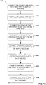
- FIG. 14 illustrates a methodology in accordance with one or more embodiments. While the methodology shown herein is shown as a series of acts, the subject innovation is not limited by the order of acts, as some acts may, in accordance therewith, occur in a different order and/or concurrently with other acts from that shown and described herein. For example, those skilled in the art will understand and appreciate that a methodology could alternatively be represented as a series of interrelated states or events, such as in a state diagram. Moreover, not all illustrated acts may be required to implement a methodology in accordance with the innovation. Furthermore, interaction diagram(s) may represent methodologies, or methods, in accordance with the subject disclosure when disparate entities enact disparate portions of the methodologies. Further yet, two or more of the disclosed example methods can be implemented in combination with each other, to accomplish one or more features or advantages described herein.
- FIG. 14 is a flow diagram of an embodiment for assembling a decoupling capacitor (DCAP) circuit.
- the DCAP circuit can be used, for example as a component of power distribution networks (PDNs).
- Method 1400 can begin at block 1402, where the source and body of a first p-channel field effect transistor (PFET) is connected to a supply voltage (e.g., a supply voltage of a power distribution network or other system requiring supply noise suppression).
- PFET p-channel field effect transistor
- NFET n-channel field effect transistor
- the drain of the first PFET is connected to the gate of the first NFET.
- the drain of the first NFET is connected to the gate of the first PFET.
- the drain, source, and body of a second PFET is connected to the supply voltage.
- the gate of the second PFET is connected to the gate of the first PFET.
- the drain, source, and body of a second NFET is connected to ground.
- the gate of the second NFET is connected to the gate of the first NFET.
- the circuit yielded by blocks 1402-1416 can be used to suppress power supply noise, and can achieve high area efficiency as well as high frequency operation.
- either of the second PFET or the second NFET is omitted from the circuit (see, e.g., FIGS. 4 and 5 ). That is, in some embodiments, blocks 1410 and 1412 are omitted, while in other embodiments blocks 1414 and 1416 are omitted.
- Computer-readable media can include hardware media, software media, non-transitory media, or transport media.
Description
- This disclosure relates generally to a decoupling capacitor circuit design for suppressing supply noise that provides high operational frequency and high area efficiency.
- Decoupling capacitors (DCAPs) are an important component of power distribution networks (PDNs) for very-large-scale-integration (VLSI) designs. These decoupling capacitors shunt the supply noise caused by active circuit elements through the capacitor, thereby suppressing the supply noise observed by other elements of the circuit that are about to become active.
- Several considerations are important to DCAP design, including high area efficiency, robust electrical properties, and properly targeted operational frequency. However, some DCAP designs are susceptible to damage from electro-static discharge (ESD) events, particularly as the transistor designs enter into ultra-deep sub-micron and finFET process nodes. Moreover, designs intended to render the DCAP more resistant to ESD damage are often hindered by an inherent trade-off between high area efficiency and high frequency operation. One prior art solution is known from the document
US 6,268,757 B1 , in which each field-effect transistor (FET) that is used as a decoupling capacitor has its drain, source, and body coupled to a first power source voltage VDD or VSS, and its gate coupled to the other power source voltage. Another prior art solution is known from the documentUS 2007/230087 A1 , which considers using MOS transistors in decoupling capacitor structures. - In D3, a first MOS transistor, of the first conductivity type, functions as a resistor element due to an on-resistance between its source and drain. The source is connected to a first power supply wiring. A second MOS transistor, of the second conductivity type, is connected to the second power supply wiring and functions as a capacitor element and has a gate length greater than that of the first MOS transistor.
- In an embodiment, a decoupling capacitor (DCAP) circuit is provided that yields high operational frequency without sacrificing area efficiency. In order to decouple the sometimes opposing design requirements of high operational frequency and area efficiency, a p-channel field effect transistor (PFET) and an n-channel field effect transistor are connected in a half-cross-coupled (HCC) fashion, and the resulting HCC circuit is supplemented by at least one area efficient capacitance (AEC) device. The half-cross-coupled FETs address the high frequency design requirement, while the AEC device(s) address the high area efficiency requirement. As a result, the size of the HCC FETs can set the operating frequency of the circuit independently of the area efficiency, while the size of the AEC device(s) can set the area efficiency independently of the operating frequency. Thus, the DCAP design described herein eliminates the undesirable trade-off between operating frequency and area efficiency inherent in some conventional DCAP designs.
- The decoupling capacitor circuit may comprise a first p-channel field effect transistor (PFET); a first n-channel field effect transistor (NFET); and at least one capacitive device, wherein a first PFET source and a first PFET body of the first PFET are connected to a voltage supply, a first NFET source and a first NFET body of the first NFET are connected to ground, the at least one capacitive device is connected to at least one of a first PFET gate of the first PFET or a first NFET gate of the first NFET, and inclusion of the at least one capacitive device increases an area efficiency of the decoupling capacitor circuit without changing a frequency response of the decoupling capacitor circuit.
- A method for suppressing power supply noise is provided, comprising connecting a first source and a first body of a first p-channel field effect transistor (PFET) to a voltage supply; connecting a second source and a second body of an n-channel field effect transistor (NFET) to ground; connecting a first drain of the first PFET to a first gate of the NFET; connecting a second drain of the NFET to a second gate of the first PFET; connecting a third drain, a third source, and a third body of a second PFET to the voltage supply; and connecting a third gate of the second PFET to the second gate of the first PFET.
- A system for suppressing power supply noise may comprise a first p-channel field effect transistor (PFET), wherein a first PFET source and a first PFET body of the first PFET are connected to a voltage supply; a first n-channel field effect transistor (NFET), wherein a first NFET source and a first NFET body of the first NFET are connected to ground; and a second NFET, wherein a first PFET drain of the first PFET is connected to a first NFET gate of the first NFET, a first NFET drain of the first NFET is connected to a first PFET gate of the PFET, a second NFET drain, a second NFET source, and a second NFET body of the second NFET is connected to ground, and a second NFET gate of the second NFET is connected to the first NFET gate of the first NFET.
-
-
FIG. 1 is a circuit diagram illustrating an example approach to DCAP design. -
FIG. 2 is a circuit diagram illustrating an example half-cross-coupled DCAP design approach. -
FIG. 3 is a circuit diagram of an example DCAP design that provides high area efficiency and high frequency operation. -
FIG. 4 is a circuit diagram of an example DCAP design that uses a single PFET AEC device. -
FIG. 5 is a circuit diagram of an example DCAP design that uses a single NFET AEC device. -
FIG. 6 is a graph illustrating the frequency response for the DCAP circuit ofFIG. 3 for various sizes of AEC devices. -
FIG. 7 is a circuit diagram of an example DCAP design that includes an AEC device comprising a PFET having a gate tied to the NG node, a source and drain tied to ground, and a body tied to VDD. -
FIG. 8 is a circuit diagram of an example DCAP design that includes an AEC device comprising an NFET having a gate tied to node PG, a drain and source tied to VDD, and body tied to ground. -
FIG. 9 is a circuit diagram of an example DCAP design that includes a PFET AEC device ofFIG. 7 and an NFET AEC device ofFIG. 8 . -
FIG. 10 is a circuit diagram of an example DCAP design that includes a first PFET AEC device ofFIG. 4 and a second PFET AEC device ofFIG. 7 . -
FIG. 11 is a circuit diagram of an example DCAP design that includes a first NFET AEC device ofFIG. 5 and a second NFET AEC device ofFIG. 8 . -
FIG. 12 is a circuit diagram of an example DCAP design that includes a PFET AEC device ofFIG. 4 and an NFET AEC device ofFIG. 8 . -
FIG. 13 is a circuit diagram of an example DCAP design that includes an NFET AEC device ofFIG. 5 and a PFET AEC device ofFIG. 7 . -
FIG. 14 illustrates a flow diagram of an embodiment for manufacturing a decoupling capacitor (DCAP) circuit. - The example DCAP designs of
figures 3 and7 - 13 do not form part of the claimed invention. - DCAPs are often used in power distribution networks of VLSI systems to suppress voltage supply noise or ripples induced by active circuit elements, thereby shielding other elements of the circuit from power supply voltage fluctuations that may damage the elements or impede their functions. Robust DCAP designs are characterized by high area efficiency, robust electrical properties, and properly targeted operational frequency. In the case of on-die DCAP design, the targeted operational frequency ranges from the operating frequency to the switching slew of the gates in the design, thus constituting the high operational frequency of the DCAP used in the power distribution network.
-
FIG. 1 is a circuit diagram illustrating one approach to DCAP design. According to this design approach, the drain, source, and body of the p-channel field effect transistor (PFET) 102 is directly tied to thesupply voltage 106, and the drain, source, and body of the n-channel field effect transistor (NFET) 104 is tied to ground. Thegate 110 of thePFET 102 is tied to ground, and thegate 112 of the NFET 104 is tied to thesupply voltage 106. This design can decouple supply noise to high operating frequencies while being area efficient. However, as the transistor designs enter into ultra-deep sub-micron and finFET process nodes, the gate oxides become exceedingly thin. Consequently, the design inFIG. 1 can become vulnerable to electro-static discharge (ESD) events that may cause damage to the gate oxide and short out the supply and ground nodes. Since thegates FIG. 1 may not be able to tolerate extreme ESD events even in the presence of ESD clamps. Designs that use metal gate material rather than poly-silicon are particularly susceptible to this problem. -
FIG. 2 is a circuit diagram illustrating another DCAP design approach that attempts to address this issue by tying the source and body of thePFET 202 to thesupply voltage 208 and the source and body of theNFET 204 toground 206, while connecting the drain and gate nodes of the PFET and NFET in a half-cross-coupled (HCC) fashion. That is, thedrain 210 ofPFET 202 is connected to thegate 212 of NFET 204, while thedrain 214 of NFET 204 is connected to thegate 216 ofPFET 202. This design provides a resistive path from the supply voltage and ground nodes to the gate through device channels, thereby protecting the gate oxide during an ESD event until the ESD clamp can shunt the excess charge. - However, using the design in
FIG.2 , it is difficult to achieve both high area efficiency and high frequency operation. This is because the HCC connectivity places these two design targets in direct conflict. For example, to achieve high area efficiency thePFET 202 and NFET 204 would require large channels to maximize the gate area. However, these large channels would add resistance to the decoupling path, thereby limiting the type of high frequency decoupling the capacitor circuit may achieve. If the channel lengths were reduced in thePFET 202 and NFET 204 to address this concern, the area efficiency would be penalized. - Moreover, a large channel for the design depicted in
FIG. 2 will result in a high start-up time. This high start-up time is due to a "dead" zone in which the HCC nodes are brought up in states opposite to the values they require for the DCAP to function, and the design depends on the device leakage of the twoFETS - To address these and other issues, DCAP circuit designs may be provided that maintain the high frequency operation offered by the HCC DCAP's electrical properties, while also achieving high area efficiency.
FIG. 3 is a circuit diagram of anexample DCAP circuit 300 not forming part of the claimed invention that provides high area efficiency and high frequency operation. This design includes aPFET 302 and an NFET 304 connected in an HCC configuration, and area efficient capacitance (AEC)devices AEC devices AEC devices - According to this design, the drain, source, and body of
PFET AEC device 306 are connected to thesupply voltage 310, while thegate 312 is connected to the PG node produced by the HCC connections. The drain, source, and body ofNFET AEC device 308 is connected to ground 314, while thegate 316 is connected to the NG node produced by the HCC connections. - The
circuit 300 depicted inFIG. 3 allows the device channel length of the HCC devices (PFET 302 and NFET 304) - and thus the corresponding resistance of the decoupling path through the PFET and NFET - to be kept low, thereby providing high frequency supply noise decoupling. Keeping the device channel length low also increases leakage in the HCC devices, thereby keeping start-up times low for scenarios in which the HCC connectivity is initialized to the incorrect states. - Whereas the
HCC devices AEC devices AEC devices PFET 302 andNFET 304, and thus without changing the operating frequency of thecircuit 300. In some cases, optimizing theAEC devices HCC devices AEC devices FIG. 3 effectively unlocks the high frequency component from the area efficiency component, allowing the design to be optimized to address high frequency applications without sacrificing area efficiency. - While
circuit 300 includes twoAEC devices PFET 302 andNFET 304, respectively, the embodiments of the present invention may include only one AEC device.FIG. 4 illustrates an embodiment in which only thePFET AEC device 306 is connected to the HCC circuit (omitting the NFET AEC device 308), whileFIG. 5 illustrates an embodiment in which only theNFET AEC device 308 is connected (omitting the PFET AEC device 306). -
FIG. 6 is agraph 602 illustrating the frequency response forcircuit 300 for various sizes ofAEC devices graph 602 represents the frequency response for a given size ofAEC devices HCC devices circuit 300 loses its effectiveness - is characterized by 1/(RC), where R is the resistance of the decoupling path determined by the size of theHCC devices AEC devices AEC devices AEC devices HCC devices HCC devices AEC devices - In addition to
AEC devices FIG. 7 is a circuit diagram of anexample DCAP circuit 700 not forming part of the present invention that includes anAEC device 702 comprising aPFET having gate 704 tied to the NG node, source and drain tied toground 314, and body tied toVDD 310.FIG. 8 is a circuit diagram of anexample DCAP circuit 800 not forming part of the present invention that includes anAEC device 802 comprising anNFET having gate 804 tied to node PG, drain and source tied toVDD 310, and body tied toground 314.FIG. 9 is a circuit diagram of anexample DCAP circuit 900 not forming part of the present invention that includes bothAEC devices -
AEC devices FIG. 10 is a circuit diagram of anexample DCAP circuit 1000 that includesAEC device 702 andAEC device 306, whileFIG. 11 is a circuit diagram of anexample DCAP circuit 1100 not forming part of the present invention that includesAEC device 802 andAEC device 308. -
FIG. 12 is a circuit diagram of anotherexample DCAP circuit 1200 not forming part of the present invention that includesAEC devices FIG. 13 is a circuit diagram of yet anotherexample DECAP circuit 1300 not forming part of the present invention that includesAEC devices - The decoupling capacitor circuits described above and illustrated in
FIGs. 3-5 andFIGS. 7-13 can be embodied using any suitable FET implementation. For example, any ofcircuits circuits -
FIG. 14 illustrates a methodology in accordance with one or more embodiments. While the methodology shown herein is shown as a series of acts, the subject innovation is not limited by the order of acts, as some acts may, in accordance therewith, occur in a different order and/or concurrently with other acts from that shown and described herein. For example, those skilled in the art will understand and appreciate that a methodology could alternatively be represented as a series of interrelated states or events, such as in a state diagram. Moreover, not all illustrated acts may be required to implement a methodology in accordance with the innovation. Furthermore, interaction diagram(s) may represent methodologies, or methods, in accordance with the subject disclosure when disparate entities enact disparate portions of the methodologies. Further yet, two or more of the disclosed example methods can be implemented in combination with each other, to accomplish one or more features or advantages described herein. -
FIG. 14 is a flow diagram of an embodiment for assembling a decoupling capacitor (DCAP) circuit. The DCAP circuit can be used, for example as a component of power distribution networks (PDNs).Method 1400 can begin atblock 1402, where the source and body of a first p-channel field effect transistor (PFET) is connected to a supply voltage (e.g., a supply voltage of a power distribution network or other system requiring supply noise suppression). Atblock 1404, the source and body of a first n-channel field effect transistor (NFET) is connected to ground. Atblock 1406, the drain of the first PFET is connected to the gate of the first NFET. Atblock 1408, the drain of the first NFET is connected to the gate of the first PFET. - At
block 1410 the drain, source, and body of a second PFET is connected to the supply voltage. Atblock 1412, the gate of the second PFET is connected to the gate of the first PFET. Atblock 1414, the drain, source, and body of a second NFET is connected to ground. Atblock 1416, the gate of the second NFET is connected to the gate of the first NFET. The circuit yielded by blocks 1402-1416 can be used to suppress power supply noise, and can achieve high area efficiency as well as high frequency operation. - In the embodiments, either of the second PFET or the second NFET is omitted from the circuit (see, e.g.,
FIGS. 4 and5 ). That is, in some embodiments, blocks 1410 and 1412 are omitted, while in other embodiments blocks 1414 and 1416 are omitted. - The disclosed subject matter can be implemented as a method, apparatus, or article of manufacture using typical manufacturing, programming or engineering techniques to produce hardware, firmware, software, or any suitable combination thereof to control an electronic device to implement the disclosed subject matter. Computer-readable media can include hardware media, software media, non-transitory media, or transport media.
Claims (7)
- A system for suppressing power supply noise, comprising:a first p-channel field effect transistor, PFET, (302), wherein a first PFET source and a first PFET body of the first PFET (302) are connected to a voltage supply (VDD);a first n-channel field effect transistor, NFET, (304), wherein a first NFET source and a first NFET body of the first NFET (304) are connected to ground (314); andat least one capacitive device comprising a single one of a second NFET (308) and a second PFET (306),whereinthe first PFET (302) and the first NFET (304) are connected in a half-cross-coupled configuration so that:a first PFET drain of the first PFET (302) is connected to a first NFET gate (NG) of the first NFET (304) without connection of the first PFET drain of the first PFET (302) or the first NFET gate (NG) of the first NFET (304) to the voltage supply (VDD),a first NFET drain of the first NFET (304) is connected to a first PFET gate (PG) of the first PFET (302) without connection of the first NFET drain of the first NFET (304) or the first PFET gate (PG) of the first PFET (302) to ground (314),in an instance when the at least one capacitive device comprises a single second NFET (308) without the second PFET (306), a second NFET drain, a second NFET source, and a second NFET body of the second NFET (308) are connected to ground (314), and a second NFET gate (NG) of the second NFET (308) is connected to the first NFET gate (NG) of the first NFET (304) without connection of the second NFET gate (NG) of the second NFET (308) to ground (314) or to the voltage supply (VDD), andin an instance when the at least one capacitive device comprises a single second PFET (306) without the second NFET (308), a second PFET drain, a second PFET source, and a second PFET body of the second PFET (306) are connected to the voltage supply (VDD), and a second PFET gate (PG) of the second PFET (306) is connected to the first PFET gate (PG) of the first PFET (302) without connection of the second PFET gate (PG) of the second PFET (306) to the voltage supply (VDD) or to ground (314).
- The system of claim 1, wherein
the voltage supply (VDD) is a voltage supply of a power distribution network of a very-large-scale-integration, VLSI, system. - The system of claim 2, wherein the system is an on-chip component of the VLSI system.
- The system of claim 2, wherein the system is an off-chip component of the VLSI system.
- A method for suppressing power supply noise, comprising:connecting a first p-channel field effect transistor, PFET, (302) and a first n-channel field effect transistor, NFET, (304) in a half-cross-coupled configuration, comprisingconnecting (1402) the source and the body of the first PFET (302) to a voltage supply (VDD);connecting (1404) the source and the body of the first NFET (304) to ground (314);connecting (1406) the drain of the first PFET (302) to the gate (NG) of the first NFET (304) without connecting the drain of the first PFET (302) or the gate (NG) of the first NFET (304) to the voltage supply (VDD);connecting (1408) the drain of the first NFET (304) to the gate (PG) of the first PFET (302) without connecting the drain of the first NFET (304) or the gate (PG) of the first PFET (302) to ground (314); andconnecting the first PFET (302) and first NFET (304) half-cross-coupled configuration to a single one of a second NFET (308) and a second PFET (306), whereinconnecting the first PFET (302) and first NFET (304) half-cross-coupled configuration to a second NFET (308) comprises:connecting (1414) the drain, source, and body of the second NFET (308) to the ground (314), andconnecting (1416) the gate (NG) of the second NFET (308) to the gate (NG) of the first NFET (304) without connecting the gate (NG) of the second NFET (308) to ground (314) or to the voltage supply (VDD); andconnecting the first PFET (302) and first NFET (304) half-cross-coupled configuration to a second PFET (306) comprises:connecting (1410) the drain, source, and body of the second PFET (306) to the voltage supply (VDD), andconnecting (1412) the gate (PG) of the second PFET (306) to the gate (PG) of the first PFET (302) without connecting the gate (PG) of the second PFET (306) to the voltage supply (VDD) or to ground (314).
- The method of claim 5, comprising connecting the first PFET (302) and first NFET (304) half-cross-coupled configuration to the second NFET (308) without the second PFET (306).
- The method of claim 5, comprising connecting the first PFET (302) and first NFET (304) half-cross-coupled configuration to the second PFET (306) without the second NFET (308).
Priority Applications (1)
| Application Number | Priority Date | Filing Date | Title |
|---|---|---|---|
| EP21193202.5A EP3934101A3 (en) | 2015-06-11 | 2015-07-30 | High efficiency half-cross-coupled decoupling capacitor |
Applications Claiming Priority (2)
| Application Number | Priority Date | Filing Date | Title |
|---|---|---|---|
| US14/736,882 US9438225B1 (en) | 2015-06-11 | 2015-06-11 | High efficiency half-cross-coupled decoupling capacitor |
| PCT/US2015/042798 WO2016200411A1 (en) | 2015-06-11 | 2015-07-30 | High efficiency half-cross-coupled decoupling capacitor |
Related Child Applications (2)
| Application Number | Title | Priority Date | Filing Date |
|---|---|---|---|
| EP21193202.5A Division-Into EP3934101A3 (en) | 2015-06-11 | 2015-07-30 | High efficiency half-cross-coupled decoupling capacitor |
| EP21193202.5A Division EP3934101A3 (en) | 2015-06-11 | 2015-07-30 | High efficiency half-cross-coupled decoupling capacitor |
Publications (3)
| Publication Number | Publication Date |
|---|---|
| EP3308464A1 EP3308464A1 (en) | 2018-04-18 |
| EP3308464A4 EP3308464A4 (en) | 2019-05-08 |
| EP3308464B1 true EP3308464B1 (en) | 2021-10-06 |
Family
ID=56878301
Family Applications (2)
| Application Number | Title | Priority Date | Filing Date |
|---|---|---|---|
| EP15895123.6A Active EP3308464B1 (en) | 2015-06-11 | 2015-07-30 | High efficiency half-cross-coupled decoupling capacitor |
| EP21193202.5A Pending EP3934101A3 (en) | 2015-06-11 | 2015-07-30 | High efficiency half-cross-coupled decoupling capacitor |
Family Applications After (1)
| Application Number | Title | Priority Date | Filing Date |
|---|---|---|---|
| EP21193202.5A Pending EP3934101A3 (en) | 2015-06-11 | 2015-07-30 | High efficiency half-cross-coupled decoupling capacitor |
Country Status (5)
| Country | Link |
|---|---|
| US (1) | US9438225B1 (en) |
| EP (2) | EP3308464B1 (en) |
| JP (1) | JP6437674B2 (en) |
| CN (1) | CN108141214B (en) |
| WO (1) | WO2016200411A1 (en) |
Families Citing this family (4)
| Publication number | Priority date | Publication date | Assignee | Title |
|---|---|---|---|---|
| US10032763B2 (en) * | 2016-06-02 | 2018-07-24 | Qualcomm Incorporated | Bulk cross-coupled high density power supply decoupling capacitor |
| US10892260B2 (en) * | 2019-03-06 | 2021-01-12 | Himax Technologies Limited | Capacitor |
| US11244895B2 (en) | 2020-06-01 | 2022-02-08 | Qualcomm Incorporated | Intertwined well connection and decoupling capacitor layout structure for integrated circuits |
| KR20220043738A (en) | 2020-09-29 | 2022-04-05 | 삼성전자주식회사 | Integrated circuit including asymmetric decoupling cell and method for designing the same |
Citations (1)
| Publication number | Priority date | Publication date | Assignee | Title |
|---|---|---|---|---|
| US20070230087A1 (en) * | 2006-03-31 | 2007-10-04 | Fujitsu Limited | Decoupling capacitor for semiconductor integrated circuit device |
Family Cites Families (24)
| Publication number | Priority date | Publication date | Assignee | Title |
|---|---|---|---|---|
| US5266848A (en) * | 1990-03-28 | 1993-11-30 | Hitachi, Ltd. | CMOS circuit with reduced signal swing |
| SE470415B (en) | 1992-07-06 | 1994-02-14 | Ericsson Telefon Ab L M | High capacitor capacitor in an integrated function block or integrated circuit, method of producing the capacitor and using the capacitor as an integrated decoupling capacitor |
| JPH08102652A (en) | 1994-10-03 | 1996-04-16 | Seiko Epson Corp | Semiconductor integrated circuit |
| JPH08307229A (en) | 1995-04-28 | 1996-11-22 | Fuji Electric Co Ltd | Load driving circuit |
| JPH0993111A (en) | 1995-09-28 | 1997-04-04 | Toshiba Microelectron Corp | Slew rate type buffer circuit |
| JPH09148909A (en) | 1995-11-17 | 1997-06-06 | Hitachi Ltd | Semiconductor integrated circuit device |
| US5883423A (en) * | 1996-02-23 | 1999-03-16 | National Semiconductor Corporation | Decoupling capacitor for integrated circuit signal driver |
| JPH11186497A (en) * | 1997-12-17 | 1999-07-09 | Toshiba Corp | Semiconductor integrated circuit device |
| JP3838769B2 (en) | 1997-12-25 | 2006-10-25 | 川崎マイクロエレクトロニクス株式会社 | Output buffer circuit |
| JP2000286388A (en) * | 1999-03-30 | 2000-10-13 | Advantest Corp | Semiconductor device |
| US6936917B2 (en) | 2001-09-26 | 2005-08-30 | Molex Incorporated | Power delivery connector for integrated circuits utilizing integrated capacitors |
| JP4342833B2 (en) * | 2003-05-16 | 2009-10-14 | Necエレクトロニクス株式会社 | Capacitance cell, semiconductor device and manufacturing method thereof |
| KR100592787B1 (en) | 2004-11-09 | 2006-06-26 | 삼성전자주식회사 | integrated circuit chip package having ring-shaped silicon decoupling capacitor |
| JP2006203801A (en) * | 2005-01-24 | 2006-08-03 | Fujitsu Ltd | Buffer circuit and integrated circuit |
| US8160824B2 (en) | 2005-01-27 | 2012-04-17 | Electro Industries/Gauge Tech | Intelligent electronic device with enhanced power quality monitoring and communication capabilities |
| JP4841204B2 (en) * | 2005-08-31 | 2011-12-21 | ルネサスエレクトロニクス株式会社 | Semiconductor device |
| US7903679B1 (en) | 2006-04-11 | 2011-03-08 | Altera Corporation | Power supply filtering for programmable logic device having heterogeneous serial interface architecture |
| US8134824B2 (en) * | 2008-02-19 | 2012-03-13 | Arm Limited | Decoupling capacitors |
| JP2009246062A (en) * | 2008-03-31 | 2009-10-22 | Hitachi Ltd | Semiconductor integrated circuit apparatus and method of manufacturing the same |
| US8345396B2 (en) * | 2010-03-08 | 2013-01-01 | Macronix International Co., Ltd. | Electrostatic discharge protectors having increased RC delays |
| US8539422B2 (en) | 2011-02-24 | 2013-09-17 | Cadence Design Systems, Inc. | Method and system for power delivery network analysis |
| US9029173B2 (en) | 2011-10-18 | 2015-05-12 | Monolithic 3D Inc. | Method for fabrication of a semiconductor device and structure |
| CN103959457B (en) * | 2011-11-14 | 2016-10-12 | 日本电气株式会社 | Decoupling circuit and semiconductor integrated circuit |
| US8963575B2 (en) * | 2012-09-26 | 2015-02-24 | Sandisk Technologies Inc. | Analog majority vote circuit |
-
2015
- 2015-06-11 US US14/736,882 patent/US9438225B1/en active Active
- 2015-07-30 EP EP15895123.6A patent/EP3308464B1/en active Active
- 2015-07-30 WO PCT/US2015/042798 patent/WO2016200411A1/en active Application Filing
- 2015-07-30 JP JP2017564018A patent/JP6437674B2/en active Active
- 2015-07-30 CN CN201580080820.9A patent/CN108141214B/en active Active
- 2015-07-30 EP EP21193202.5A patent/EP3934101A3/en active Pending
Patent Citations (1)
| Publication number | Priority date | Publication date | Assignee | Title |
|---|---|---|---|---|
| US20070230087A1 (en) * | 2006-03-31 | 2007-10-04 | Fujitsu Limited | Decoupling capacitor for semiconductor integrated circuit device |
Also Published As
| Publication number | Publication date |
|---|---|
| EP3308464A4 (en) | 2019-05-08 |
| EP3308464A1 (en) | 2018-04-18 |
| WO2016200411A1 (en) | 2016-12-15 |
| EP3934101A3 (en) | 2022-04-27 |
| EP3934101A2 (en) | 2022-01-05 |
| JP6437674B2 (en) | 2018-12-12 |
| CN108141214A (en) | 2018-06-08 |
| US9438225B1 (en) | 2016-09-06 |
| JP2018521504A (en) | 2018-08-02 |
| CN108141214B (en) | 2019-06-11 |
Similar Documents
| Publication | Publication Date | Title |
|---|---|---|
| TWI539708B (en) | Electrostatic discharge protection circuit | |
| EP3308464B1 (en) | High efficiency half-cross-coupled decoupling capacitor | |
| US8743515B2 (en) | ESD clamp with novel RC triggered circuit | |
| US9379707B2 (en) | Decoupling circuit and semiconductor integrated circuit | |
| US10591532B2 (en) | Semiconductor integrated circuit | |
| JP2014132717A (en) | Electrostatic discharge protection circuit and semiconductor circuit device | |
| US8345396B2 (en) | Electrostatic discharge protectors having increased RC delays | |
| US10404265B1 (en) | Current-mode feedback source follower with enhanced linearity | |
| US9859704B2 (en) | Node isolation for protection from electrostatic discharge (ESD) damage | |
| CN103247697A (en) | Decoupling capacitor and integrated circuit provided with same | |
| KR102101537B1 (en) | Tie-High/Tie-Low Circuit | |
| US7087968B1 (en) | Electrostatic discharge protection circuit and semiconductor circuit therewith | |
| CN105097799A (en) | Signal receiving circuit and signal transceiving circuit | |
| US20190214983A1 (en) | Clock voltage step-up circuit | |
| US10211823B2 (en) | Method and apparatus for protecting gate-source junction of low-voltage MOSFET in high-voltage circuit | |
| US10153272B2 (en) | Semiconductor integrated circuit | |
| US10917084B2 (en) | Output driving system with capacitance compensation | |
| US10320351B1 (en) | Switch for controlling a gain of an amplifier and method thereof | |
| TWI485542B (en) | Circuit and method for power supply | |
| JP2015159137A (en) | ESD protection circuit | |
| TWI234264B (en) | ESD protection circuit with a stack-coupling device | |
| CN110263468B (en) | On-chip CMOS capacitor and chip | |
| JP2005085980A (en) | Fuse circuit | |
| JP2014204602A (en) | Semiconductor device |
Legal Events
| Date | Code | Title | Description |
|---|---|---|---|
| STAA | Information on the status of an ep patent application or granted ep patent |
Free format text: STATUS: THE INTERNATIONAL PUBLICATION HAS BEEN MADE |
|
| PUAI | Public reference made under article 153(3) epc to a published international application that has entered the european phase |
Free format text: ORIGINAL CODE: 0009012 |
|
| STAA | Information on the status of an ep patent application or granted ep patent |
Free format text: STATUS: REQUEST FOR EXAMINATION WAS MADE |
|
| 17P | Request for examination filed |
Effective date: 20171207 |
|
| AK | Designated contracting states |
Kind code of ref document: A1 Designated state(s): AL AT BE BG CH CY CZ DE DK EE ES FI FR GB GR HR HU IE IS IT LI LT LU LV MC MK MT NL NO PL PT RO RS SE SI SK SM TR |
|
| AX | Request for extension of the european patent |
Extension state: BA ME |
|
| RAP1 | Party data changed (applicant data changed or rights of an application transferred) |
Owner name: AMPERE COMPUTING LLC |
|
| DAV | Request for validation of the european patent (deleted) | ||
| DAX | Request for extension of the european patent (deleted) | ||
| A4 | Supplementary search report drawn up and despatched |
Effective date: 20190409 |
|
| RIC1 | Information provided on ipc code assigned before grant |
Ipc: H01L 27/08 20060101ALN20190403BHEP Ipc: H03K 19/094 20060101AFI20190403BHEP Ipc: H01L 29/94 20060101ALN20190403BHEP Ipc: H01L 27/02 20060101ALI20190403BHEP Ipc: H01L 27/06 20060101ALI20190403BHEP |
|
| STAA | Information on the status of an ep patent application or granted ep patent |
Free format text: STATUS: EXAMINATION IS IN PROGRESS |
|
| 17Q | First examination report despatched |
Effective date: 20200210 |
|
| STAA | Information on the status of an ep patent application or granted ep patent |
Free format text: STATUS: EXAMINATION IS IN PROGRESS |
|
| REG | Reference to a national code |
Ref country code: DE Ref legal event code: R079 Ref document number: 602015074025 Country of ref document: DE Free format text: PREVIOUS MAIN CLASS: H03K0019094000 Ipc: H01L0027020000 |
|
| GRAP | Despatch of communication of intention to grant a patent |
Free format text: ORIGINAL CODE: EPIDOSNIGR1 |
|
| STAA | Information on the status of an ep patent application or granted ep patent |
Free format text: STATUS: GRANT OF PATENT IS INTENDED |
|
| RIC1 | Information provided on ipc code assigned before grant |
Ipc: H01L 27/02 20060101AFI20210325BHEP Ipc: H01L 27/06 20060101ALI20210325BHEP Ipc: H01L 29/94 20060101ALI20210325BHEP Ipc: H01L 27/08 20060101ALN20210325BHEP |
|
| RIC1 | Information provided on ipc code assigned before grant |
Ipc: H01L 27/02 20060101AFI20210412BHEP Ipc: H01L 27/06 20060101ALI20210412BHEP Ipc: H01L 29/94 20060101ALI20210412BHEP Ipc: H01L 27/08 20060101ALN20210412BHEP |
|
| INTG | Intention to grant announced |
Effective date: 20210428 |
|
| GRAS | Grant fee paid |
Free format text: ORIGINAL CODE: EPIDOSNIGR3 |
|
| GRAA | (expected) grant |
Free format text: ORIGINAL CODE: 0009210 |
|
| STAA | Information on the status of an ep patent application or granted ep patent |
Free format text: STATUS: THE PATENT HAS BEEN GRANTED |
|
| AK | Designated contracting states |
Kind code of ref document: B1 Designated state(s): AL AT BE BG CH CY CZ DE DK EE ES FI FR GB GR HR HU IE IS IT LI LT LU LV MC MK MT NL NO PL PT RO RS SE SI SK SM TR |
|
| REG | Reference to a national code |
Ref country code: GB Ref legal event code: FG4D |
|
| REG | Reference to a national code |
Ref country code: CH Ref legal event code: EP Ref country code: AT Ref legal event code: REF Ref document number: 1436955 Country of ref document: AT Kind code of ref document: T Effective date: 20211015 |
|
| REG | Reference to a national code |
Ref country code: IE Ref legal event code: FG4D |
|
| REG | Reference to a national code |
Ref country code: DE Ref legal event code: R096 Ref document number: 602015074025 Country of ref document: DE |
|
| REG | Reference to a national code |
Ref country code: LT Ref legal event code: MG9D |
|
| REG | Reference to a national code |
Ref country code: NL Ref legal event code: MP Effective date: 20211006 |
|
| REG | Reference to a national code |
Ref country code: AT Ref legal event code: MK05 Ref document number: 1436955 Country of ref document: AT Kind code of ref document: T Effective date: 20211006 |
|
| PG25 | Lapsed in a contracting state [announced via postgrant information from national office to epo] |
Ref country code: RS Free format text: LAPSE BECAUSE OF FAILURE TO SUBMIT A TRANSLATION OF THE DESCRIPTION OR TO PAY THE FEE WITHIN THE PRESCRIBED TIME-LIMIT Effective date: 20211006 Ref country code: LT Free format text: LAPSE BECAUSE OF FAILURE TO SUBMIT A TRANSLATION OF THE DESCRIPTION OR TO PAY THE FEE WITHIN THE PRESCRIBED TIME-LIMIT Effective date: 20211006 Ref country code: FI Free format text: LAPSE BECAUSE OF FAILURE TO SUBMIT A TRANSLATION OF THE DESCRIPTION OR TO PAY THE FEE WITHIN THE PRESCRIBED TIME-LIMIT Effective date: 20211006 Ref country code: BG Free format text: LAPSE BECAUSE OF FAILURE TO SUBMIT A TRANSLATION OF THE DESCRIPTION OR TO PAY THE FEE WITHIN THE PRESCRIBED TIME-LIMIT Effective date: 20220106 Ref country code: AT Free format text: LAPSE BECAUSE OF FAILURE TO SUBMIT A TRANSLATION OF THE DESCRIPTION OR TO PAY THE FEE WITHIN THE PRESCRIBED TIME-LIMIT Effective date: 20211006 |
|
| PG25 | Lapsed in a contracting state [announced via postgrant information from national office to epo] |
Ref country code: IS Free format text: LAPSE BECAUSE OF FAILURE TO SUBMIT A TRANSLATION OF THE DESCRIPTION OR TO PAY THE FEE WITHIN THE PRESCRIBED TIME-LIMIT Effective date: 20220206 Ref country code: SE Free format text: LAPSE BECAUSE OF FAILURE TO SUBMIT A TRANSLATION OF THE DESCRIPTION OR TO PAY THE FEE WITHIN THE PRESCRIBED TIME-LIMIT Effective date: 20211006 Ref country code: PT Free format text: LAPSE BECAUSE OF FAILURE TO SUBMIT A TRANSLATION OF THE DESCRIPTION OR TO PAY THE FEE WITHIN THE PRESCRIBED TIME-LIMIT Effective date: 20220207 Ref country code: PL Free format text: LAPSE BECAUSE OF FAILURE TO SUBMIT A TRANSLATION OF THE DESCRIPTION OR TO PAY THE FEE WITHIN THE PRESCRIBED TIME-LIMIT Effective date: 20211006 Ref country code: NO Free format text: LAPSE BECAUSE OF FAILURE TO SUBMIT A TRANSLATION OF THE DESCRIPTION OR TO PAY THE FEE WITHIN THE PRESCRIBED TIME-LIMIT Effective date: 20220106 Ref country code: NL Free format text: LAPSE BECAUSE OF FAILURE TO SUBMIT A TRANSLATION OF THE DESCRIPTION OR TO PAY THE FEE WITHIN THE PRESCRIBED TIME-LIMIT Effective date: 20211006 Ref country code: LV Free format text: LAPSE BECAUSE OF FAILURE TO SUBMIT A TRANSLATION OF THE DESCRIPTION OR TO PAY THE FEE WITHIN THE PRESCRIBED TIME-LIMIT Effective date: 20211006 Ref country code: HR Free format text: LAPSE BECAUSE OF FAILURE TO SUBMIT A TRANSLATION OF THE DESCRIPTION OR TO PAY THE FEE WITHIN THE PRESCRIBED TIME-LIMIT Effective date: 20211006 Ref country code: GR Free format text: LAPSE BECAUSE OF FAILURE TO SUBMIT A TRANSLATION OF THE DESCRIPTION OR TO PAY THE FEE WITHIN THE PRESCRIBED TIME-LIMIT Effective date: 20220107 Ref country code: ES Free format text: LAPSE BECAUSE OF FAILURE TO SUBMIT A TRANSLATION OF THE DESCRIPTION OR TO PAY THE FEE WITHIN THE PRESCRIBED TIME-LIMIT Effective date: 20211006 |
|
| REG | Reference to a national code |
Ref country code: DE Ref legal event code: R097 Ref document number: 602015074025 Country of ref document: DE |
|
| PG25 | Lapsed in a contracting state [announced via postgrant information from national office to epo] |
Ref country code: SM Free format text: LAPSE BECAUSE OF FAILURE TO SUBMIT A TRANSLATION OF THE DESCRIPTION OR TO PAY THE FEE WITHIN THE PRESCRIBED TIME-LIMIT Effective date: 20211006 Ref country code: SK Free format text: LAPSE BECAUSE OF FAILURE TO SUBMIT A TRANSLATION OF THE DESCRIPTION OR TO PAY THE FEE WITHIN THE PRESCRIBED TIME-LIMIT Effective date: 20211006 Ref country code: RO Free format text: LAPSE BECAUSE OF FAILURE TO SUBMIT A TRANSLATION OF THE DESCRIPTION OR TO PAY THE FEE WITHIN THE PRESCRIBED TIME-LIMIT Effective date: 20211006 Ref country code: EE Free format text: LAPSE BECAUSE OF FAILURE TO SUBMIT A TRANSLATION OF THE DESCRIPTION OR TO PAY THE FEE WITHIN THE PRESCRIBED TIME-LIMIT Effective date: 20211006 Ref country code: DK Free format text: LAPSE BECAUSE OF FAILURE TO SUBMIT A TRANSLATION OF THE DESCRIPTION OR TO PAY THE FEE WITHIN THE PRESCRIBED TIME-LIMIT Effective date: 20211006 Ref country code: CZ Free format text: LAPSE BECAUSE OF FAILURE TO SUBMIT A TRANSLATION OF THE DESCRIPTION OR TO PAY THE FEE WITHIN THE PRESCRIBED TIME-LIMIT Effective date: 20211006 |
|
| PLBE | No opposition filed within time limit |
Free format text: ORIGINAL CODE: 0009261 |
|
| STAA | Information on the status of an ep patent application or granted ep patent |
Free format text: STATUS: NO OPPOSITION FILED WITHIN TIME LIMIT |
|
| 26N | No opposition filed |
Effective date: 20220707 |
|
| PG25 | Lapsed in a contracting state [announced via postgrant information from national office to epo] |
Ref country code: AL Free format text: LAPSE BECAUSE OF FAILURE TO SUBMIT A TRANSLATION OF THE DESCRIPTION OR TO PAY THE FEE WITHIN THE PRESCRIBED TIME-LIMIT Effective date: 20211006 |
|
| PG25 | Lapsed in a contracting state [announced via postgrant information from national office to epo] |
Ref country code: SI Free format text: LAPSE BECAUSE OF FAILURE TO SUBMIT A TRANSLATION OF THE DESCRIPTION OR TO PAY THE FEE WITHIN THE PRESCRIBED TIME-LIMIT Effective date: 20211006 |
|
| PG25 | Lapsed in a contracting state [announced via postgrant information from national office to epo] |
Ref country code: MC Free format text: LAPSE BECAUSE OF FAILURE TO SUBMIT A TRANSLATION OF THE DESCRIPTION OR TO PAY THE FEE WITHIN THE PRESCRIBED TIME-LIMIT Effective date: 20211006 |
|
| REG | Reference to a national code |
Ref country code: CH Ref legal event code: PL |
|
| REG | Reference to a national code |
Ref country code: BE Ref legal event code: MM Effective date: 20220731 |
|
| PG25 | Lapsed in a contracting state [announced via postgrant information from national office to epo] |
Ref country code: LU Free format text: LAPSE BECAUSE OF NON-PAYMENT OF DUE FEES Effective date: 20220730 Ref country code: LI Free format text: LAPSE BECAUSE OF NON-PAYMENT OF DUE FEES Effective date: 20220731 Ref country code: FR Free format text: LAPSE BECAUSE OF NON-PAYMENT OF DUE FEES Effective date: 20220731 Ref country code: CH Free format text: LAPSE BECAUSE OF NON-PAYMENT OF DUE FEES Effective date: 20220731 |
|
| PG25 | Lapsed in a contracting state [announced via postgrant information from national office to epo] |
Ref country code: IT Free format text: LAPSE BECAUSE OF FAILURE TO SUBMIT A TRANSLATION OF THE DESCRIPTION OR TO PAY THE FEE WITHIN THE PRESCRIBED TIME-LIMIT Effective date: 20211006 Ref country code: BE Free format text: LAPSE BECAUSE OF NON-PAYMENT OF DUE FEES Effective date: 20220731 |
|
| PG25 | Lapsed in a contracting state [announced via postgrant information from national office to epo] |
Ref country code: IE Free format text: LAPSE BECAUSE OF NON-PAYMENT OF DUE FEES Effective date: 20220730 |
|
| PGFP | Annual fee paid to national office [announced via postgrant information from national office to epo] |
Ref country code: GB Payment date: 20230721 Year of fee payment: 9 |
|
| PGFP | Annual fee paid to national office [announced via postgrant information from national office to epo] |
Ref country code: DE Payment date: 20230719 Year of fee payment: 9 |
|
| PG25 | Lapsed in a contracting state [announced via postgrant information from national office to epo] |
Ref country code: HU Free format text: LAPSE BECAUSE OF FAILURE TO SUBMIT A TRANSLATION OF THE DESCRIPTION OR TO PAY THE FEE WITHIN THE PRESCRIBED TIME-LIMIT; INVALID AB INITIO Effective date: 20150730 |