EP3306739B1 - Hohlraumfilter - Google Patents
Hohlraumfilter Download PDFInfo
- Publication number
- EP3306739B1 EP3306739B1 EP16837278.7A EP16837278A EP3306739B1 EP 3306739 B1 EP3306739 B1 EP 3306739B1 EP 16837278 A EP16837278 A EP 16837278A EP 3306739 B1 EP3306739 B1 EP 3306739B1
- Authority
- EP
- European Patent Office
- Prior art keywords
- cavity
- standard
- module
- metal layer
- substrate
- Prior art date
- Legal status (The legal status is an assumption and is not a legal conclusion. Google has not performed a legal analysis and makes no representation as to the accuracy of the status listed.)
- Active
Links
Images


Classifications
-
- H—ELECTRICITY
- H01—ELECTRIC ELEMENTS
- H01P—WAVEGUIDES; RESONATORS, LINES, OR OTHER DEVICES OF THE WAVEGUIDE TYPE
- H01P1/00—Auxiliary devices
- H01P1/20—Frequency-selective devices, e.g. filters
- H01P1/201—Filters for transverse electromagnetic waves
- H01P1/205—Comb or interdigital filters; Cascaded coaxial cavities
- H01P1/2053—Comb or interdigital filters; Cascaded coaxial cavities the coaxial cavity resonators being disposed parall to each other
-
- H—ELECTRICITY
- H01—ELECTRIC ELEMENTS
- H01P—WAVEGUIDES; RESONATORS, LINES, OR OTHER DEVICES OF THE WAVEGUIDE TYPE
- H01P1/00—Auxiliary devices
- H01P1/20—Frequency-selective devices, e.g. filters
- H01P1/201—Filters for transverse electromagnetic waves
- H01P1/205—Comb or interdigital filters; Cascaded coaxial cavities
-
- H—ELECTRICITY
- H01—ELECTRIC ELEMENTS
- H01P—WAVEGUIDES; RESONATORS, LINES, OR OTHER DEVICES OF THE WAVEGUIDE TYPE
- H01P1/00—Auxiliary devices
- H01P1/20—Frequency-selective devices, e.g. filters
- H01P1/207—Hollow waveguide filters
-
- H—ELECTRICITY
- H01—ELECTRIC ELEMENTS
- H01P—WAVEGUIDES; RESONATORS, LINES, OR OTHER DEVICES OF THE WAVEGUIDE TYPE
- H01P1/00—Auxiliary devices
- H01P1/20—Frequency-selective devices, e.g. filters
- H01P1/207—Hollow waveguide filters
- H01P1/208—Cascaded cavities; Cascaded resonators inside a hollow waveguide structure
- H01P1/2084—Cascaded cavities; Cascaded resonators inside a hollow waveguide structure with dielectric resonators
-
- H—ELECTRICITY
- H01—ELECTRIC ELEMENTS
- H01P—WAVEGUIDES; RESONATORS, LINES, OR OTHER DEVICES OF THE WAVEGUIDE TYPE
- H01P1/00—Auxiliary devices
- H01P1/20—Frequency-selective devices, e.g. filters
- H01P1/207—Hollow waveguide filters
- H01P1/208—Cascaded cavities; Cascaded resonators inside a hollow waveguide structure
- H01P1/2088—Integrated in a substrate
-
- H—ELECTRICITY
- H01—ELECTRIC ELEMENTS
- H01P—WAVEGUIDES; RESONATORS, LINES, OR OTHER DEVICES OF THE WAVEGUIDE TYPE
- H01P11/00—Apparatus or processes specially adapted for manufacturing waveguides or resonators, lines, or other devices of the waveguide type
- H01P11/008—Manufacturing resonators
-
- H—ELECTRICITY
- H01—ELECTRIC ELEMENTS
- H01P—WAVEGUIDES; RESONATORS, LINES, OR OTHER DEVICES OF THE WAVEGUIDE TYPE
- H01P7/00—Resonators of the waveguide type
- H01P7/06—Cavity resonators
Definitions
- the present disclosure relates to a cavity filter that is one of radio frequency (RF) filters.
- RF radio frequency
- a common cavity filter includes a resonance rod and a cover plate. Firstly, since a cavity of a conventional cavity filter is mostly manufactured as a whole in a die-casting process, not only the high costs of die sinking and machining are incurred but also size and weight may increase.
- Patent publication US 204/0077900 A1 discloses a dialectric waveguie filter comprising a block of dielectric material covered with an exterior layer of conductive material.
- Patent publication EP 1 732 158 A1 discloses a microwave filter comprising a plurality of coupled resonators, wherein the plurality of coupled resonators includes at least one coaxial resonator comprising a housing having a lower end wall, a sidewall extending upwardly from he lower end wall, and an upper end wall and an inner conductor disposed within the housing and extending upwardly from the lower end wall along the longitudinal axis of the housing.
- Patent publication WO 2014/047820 A1 discloses a cavity filter, relating to the field of communication, with the function of simplifying the assembling techniques and ehnancing the reuse rate of moulds.
- An embodiment of the present disclosure provides a cavity filter including a standard cavity module, by which manufacturing costs of the cavity filter are reduced, efficiency of the cavity filter is improved, and easier manufacturing of the cavity filter is facilitated.
- a cavity filter as set out in the accompanying claim 1.
- the standard cavity module may be fixed onto the metal layer for grounding by soldering.
- the standard cavity module may include a mono-standard cavity module or a dual-standard cavity module.
- the mono-standard cavity module may include a cavity body which includes an opening in an end thereof and has a pipe shape extending in a direction, and a protruding column extending from the other end of the cavity body, which faces the opening of the cavity body, and including a screw hole in an end portion thereof.
- a cavity filter as set out in the accompanying claim 2.
- the dual-standard cavity module may further include a coupling rod arranged on sidewalls between the first cavity module and the second cavity module.
- the cavity filter may further include a plurality of coupling through-holes in the PCB substrate, which are used to couple the plurality of standard cavity modules arranged on different surfaces of the PCB substrate.
- the cavity filter may further include a plurality of connectors which are fixed onto the PCB substrate and are capacitive-coupled with the plurality of standard cavity modules through the micro band layer.
- the cavity filter may further include an adjustment screw nut engaged with the screw hole of the protruding column.
- a cavity filter as set out in the accompanying claim 6.
- the standard cavity module may be fixed onto the metal layer for grounding by soldering.
- the metal layer substrate may include the metal layer electroplated on both surfaces of a ceramic substrate or may include the metal layer.
- a cavity filter as set out in the accompanying claim 8.
- the dual-standard cavity module may further include a coupling rod arranged on sidewalls between the first cavity module and the second cavity module.
- the cavity filter may further include an impedance matching line passing through the metal layer substrate, in which the impedance matching line couples a plurality of standard cavity modules arranged on the same surface of the metal layer substrate.
- the cavity filter may further include a tap piece arranged inside the standard cavity module and a plurality of connectors connected with the tap piece.
- the cavity filter may further include an adjustment screw nut engaged with the screw hole of the protruding column.
- the cavity filter according to an embodiment of the present disclosure, by fixing the standard cavity module onto the substrate by soldering, complex die-casting for the cavity module may be avoided, thus enabling size and weight reduction of a device.
- the standard cavity modules are soldered, an additional component for fixing the standard cavity module is not needed, thereby achieving cost reduction. If a standard cavity module is fixed onto a substrate using soldering in a cavity implemented as a standard module, it is possible to prevent a gap between the cavity and the substrate, which may be generated during fixing of the cavity onto the substrate using bolt engagement.
- the standard cavity module may be made smaller in size and have more excellent electroplating effect than a die-casting cavity.
- a material used for the standard cavity module is not limited to a material used for die-casting module, thus allowing use of various materials.
- coupling of standard cavity modules may be achieved using wire arrangement, thereby more easily designing the cavity filter regardless of cavity topology arrangement. Since the standard cavity modules may be arranged on both surfaces of the substrate, the space utilization rate of the cavity filter may be increased.
- PCB printed circuit board
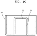
- FIGS. 1A and 1B are perspective views of a standard cavity module according to an embodiment of the present disclosure.
- FIG. 1C is a cross-sectional view of the standard cavity module shown in FIG. 1A .
- a standard cavity module according to the current embodiment may be implemented with a single module.
- a standard cavity module 2 may include a cavity body 20 including an opening at an end portion thereof, a protruding column 21 extending from the other end portion facing the end portion, and a screw hole 22 in the center of an end portion of the protruding column 21.
- the cavity body 20 may be implemented in a rectangular parallelepiped or cylinder shape. In this case, a cavity resonance space is provided inside the cavity body 20, and the protruding column 21 extends to the cavity resonance space.
- the standard cavity module 2 may be formed using sheet metal stamping or metal powder metallurgy.
- the standard cavity module 2 may include copper, iron, aluminum, an alloy, etc. If sheet metal stamping is used, a wall thickness of the cavity body 20 may be reduced and a precision may be improved. Through standard modulization of a resonance cavity, structure designing may be simplified, and costs of simulation modeling and mass production may be reduced.
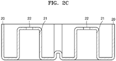
- FIGS. 2A and 2B are perspective views of a standard cavity module according to another embodiment of the present disclosure.
- FIG. 2C is a cross-sectional view of the standard cavity module shown in FIG. 2A .
- a standard cavity module according to the current embodiment may be implemented as a dual module.
- the standard cavity module 2 may include the cavity body 20 including a first body portion 201 and a second body portion 202, the protruding column 21 arranged in each of the first body portion 201 and the second body portion 202, and the screw hole 22 in the center of an end portion of each protruding column 21.
- each of the first body portion 201 and the second body portion 202 may include an opening at an end portion thereof, and each protruding column 21 may extend from the other end portion facing the end portion.
- the first body portion 201 and the second body portion 202 may be implemented in a rectangular parallelepiped or cylinder shape, and adjacent sidewalls between the first body portion 201 and the second body portion 202 are removed, such that the first body portion 201 and the second body portion 202 are connected to each other and are coupled through a coupling rod 6 (see FIG. 8 ).
- a cavity resonance space is provided inside the first body portion 201 and the second body portion 202, and the protruding column 21 extends to the cavity resonance space.
- a coupling rod may be arranged in a cavity module integrated in a mono or dual manner.
- the present disclosure is not limited thereto, and in some embodiments based on specific designing and process requirements, the standard cavity module 2 may not be limited to a mono or dual module. For example, if a topology condition is satisfied, a plurality of small cavities arranged in parallel to each other for mass production and cost reduction may be used for multi-cross coupling, and integrally formed multi-cavities may be used.
- FIG. 3 is a perspective view of the cavity filter according to an embodiment of the present disclosure.
- FIG. 4 is a perspective view of a cavity filter according to another embodiment of the present disclosure.
- FIG. 5 is a cross-sectional view of the cavity filter, taken along a line A-A shown in FIG. 4 .
- FIG. 6 is a plan view of the cavity filter shown in FIG. 3 .
- the cavity filter may include a printed circuit board (PCB) 1, a plurality of standard cavity modules 2, and a plurality of connectors 3.
- PCB printed circuit board
- Each standard cavity module 2 included in the cavity filter may be the standard cavity module 2 shown in FIGS. 1A through 2C .
- the present disclosure is not limited to the foregoing example.
- a metal layer 10 for grounding On a surface of the PCB substrate 1 may be arranged a metal layer 10 for grounding.
- the metal layer 10 for grounding may be a copper layer achieving conduction and shielding.
- the coupling window may be a solder-resist layer coupling window 11 where a solder-resist layer of the PCB substrate 1 is exposed.
- the plurality of standard cavity modules 2 are fixed onto a side or both sides of the PCB substrate 1.
- the plurality of standard cavity modules 2 may be fixed at a side or both sides of the PCB substrate 1 by soldering.
- An open end portion of the standard cavity module 2 is shielded by the metal layer 10 for grounding, such that the standard cavity module 2 is sealed.
- the plurality of standard cavity modules 2 arranged on the same surface of the PCB substrate 1 may be coupled through a micro band layer 12 provided on the PCB substrate 1.
- the plurality of standard cavity modules 2 arranged on different surfaces of the PCB substrate 1 may be coupled through the solder-resist coupling window 11.
- the plurality of connectors 3 may include an ANT connector and a TX/RX connector that are fixed onto the PCB substrate 1 by soldering.
- the ANT connector and the TX/RX connector may set capacitive coupling with the standard cavity module 2 through the micro band layer 12 provided on the PCB substrate 1.
- a PA or TRX circuit board may be integrated as a whole into the PCB substrate 1, and a function circuit equivalent to the PA or TRX circuit may be directly connected with a micro band line. In this case, by changing a shape and a size of the micro band line, the amount of coupling may be adjusted, or may be reinforced by assembling a tap piece.
- the cavity filter according to an embodiment of the present disclosure may further include an elastic sheet connection structure 4 arranged on the PCB substrate 1.
- the elastic sheet connection structure 4 may function substantially in the same manner as the plurality of connectors 3.
- the elastic sheet connection structure 4 may set capacitive coupling with the standard cavity module 2 through the micro band layer 12 provided on the PCB substrate 1.
- the elastic sheet connection structure 4 may be simply lap-jointed with an external connector or main rods of another PCB substrate.
- the cavity filter according to an embodiment of the present disclosure may further include an adjustment screw nut 5 that is arranged to be engaged with the screw hole 22 of the protruding column 21 so as to adjust a resonant frequency.
- a coupling through-hole may be arranged as a sequence cavity for tuning and coupling between two standard cavity modules.
- a hole may be formed in the PCB substrate 1 or a solder paste, etc. may be added to the PCB substrate 1.
- the standard cavity module 2 is soldered onto a surface of the PCB substrate 1 to form a sealed cavity with the grounded metal layer 10, thereby preventing a leakage between the exposed grounded metal layer 10 having the wide area on the PCB substrate 1 and the standard cavity module 2.
- an index of RF performance may be improved by integrating a resonant rod, i.e., the protruding column 21 into the cavity body 20 and forming the cavity body 20 and the protruding column 21 with the same metal material (e.g., iron or copper).
- the cavity filter may include the PCB substrate 1 and the plurality of standard cavity modules 2 fixed onto the both surfaces of the PCB substrate 1 by soldering.
- standard cavity modules a, b, c, and d may be soldered to a surface of the PCB substrate 1
- standard cavity modules e, f, g, and h may be soldered to the other surface of the PCB substrate 1, such that the plurality of standard cavity modules a, b, c, d, e, f, g, and h may be fixed onto the PCB substrate 1.
- each of the plurality of standard cavity modules a, b, c, d, e, f, g, and h may be a single standard module.
- Each of the plurality of standard cavity modules 2 arranged on the same surface of the PCB substrate 1 may be coupled through the micro band layer 12 provided on a central layer of the PCB substrate 1.
- the two adjacent standard cavity modules c and d may be coupled as sequence cavities through the central micro band layer 12.
- the standard cavity modules 2 that are not adjacent to each other may be cross-coupled as crossover cavities through the central micro band layer 12.
- a micro band line formed on the central micro band layer 12 may be arranged to connect the standard cavity modules a and d.
- a process of etching a PCB substrate may be easier than structure designing of a standard cavity module, cross coupling between non-adjacent cavities using a micro band line may be achieved easily.
- the flexibility of cavity filter designing may be largely improved, and a rate of utilization may be enhanced.
- the amount of coupling may be adjusted by changing the shape and size of the micro band line, and the amount of coupling may be increased by assembling a tap piece.
- the plurality of standard cavity modules 2 arranged on different surfaces of the PCB substrate 1 may be coupled through the solder-resist coupling window 11.
- the solder-resist coupling window 11 is marked with '*'.
- the standard cavity module a may be coupled with the standard cavity module e arranged on the other surface through the solder-resist coupling window 11.
- the standard cavity module b may be coupled with the standard cavity module g arranged on the other surface through the solder-resist coupling window 11.
- the plurality of standard cavity modules 2 arranged on different surfaces of the PCB substrate 1 may be coupled through a coupling through-hole 13 in the PCB substrate 1.
- the standard cavity module a may be coupled with the standard cavity module g arranged on the other surface of the PCB substrate 1 through the coupling through-hole 13.
- FIG. 7 is a perspective view of the cavity filter according to an embodiment of the present disclosure.
- FIG. 8 is a cross-sectional view of the cavity filter, taken along a line B-B of FIG. 7 .
- FIG. 9 is a plan view of the cavity filter shown in FIG. 7 .
- the cavity filter may include the PCB substrate 1, the plurality of standard cavity modules 2, and the plurality of connectors 3.
- Each standard cavity module 2 included in the cavity filter may be, but not limited to, the standard cavity module 2 shown in FIGS. 1A through 2C .
- the standard cavity modules c, d, g, and h may be dual-standard modules, and the other standard cavity modules a, b, e, f, and i may be mono-standard modules.
- a metal layer is formed on at least both surfaces of a metal layer substrate 7, and a via-hole coupling window 73 is arranged inside.
- the entire metal layer substrate 7 may be formed of metal, or the metal layer may be applied onto a ceramic substrate by electroplating.
- the plurality of standard cavity modules 2 are fixed onto a side or both sides of the metal layer substrate 7.
- the plurality of standard cavity modules 2 are fixed onto a side or both sides of the metal layer substrate 7 by soldering.
- An open end portion of the standard cavity module 2 is shielded by the metal layer substrate 7, such that the standard cavity module 2 is sealed.
- the plurality of standard cavity modules 2 arranged on different surfaces of the metal layer substrate 7 may be coupled by the via-hole coupling window 73.
- the via-hole coupling window 73 that satisfies size and shape requirements to form a coupling window of a sequence cavity may be arranged in a predetermined position of the metal layer substrate 7.
- the plurality of standard cavity modules 2 arranged on the same surface of the metal layer substrate 7 may be coupled by the coupling rod 6 or according to matching impedance between the standard cavity modules 2.
- the standard cavity modules c, d, g, and h formed as dual-standard modules may be coupled by the coupling rod 6.
- the standard cavity modules a, b, e, f, and i formed as mono-standard modules are formed through coupling impedance matching, and are cross-coupled by an impedance matching line passing through the metal layer substrate 7.
- a connector hole 74 in the metal layer substrate 7 connects a tap piece 8 positioned in the cavity of the standard cavity module 2 with the connector 3.
- the connector 3 may include an ANT connector and a TX/RX connector.
- the connector 3 as shown in FIG. 9 may be directly soldered onto sidewalls of a cavity of the standard cavity module 2.
- the cavity filter according to an embodiment of the present disclosure may further include an adjustment screw nut 5 that is arranged to be engaged with the screw hole 22 of the protruding column 21 so as to adjust a resonant frequency.
- FIGS. 3 through 6 Detailed information and operating principles refer to a description of FIGS. 3 through 6 , and a detailed description of the current embodiment will be omitted.
- the standard cavity module 2 is soldered onto a surface of the metal layer substrate 7 to form a sealed cavity with the metal layer substrate 7, thereby preventing a leakage between the metal layer substrate 7 and the standard cavity module 2.
- an index of RF performance may be improved by integrating a resonant rod, i.e., the protruding column 21 into the cavity body 20 and forming the cavity body 20 and the protruding column 21 with the same metal material (e.g., iron or copper).
- the cavity filter according to an embodiment of the present disclosure, by fixing the standard cavity module onto the substrate by soldering, complex die-casting for the cavity module may be avoided, thus enabling size and weight reduction of a device. Moreover, since the standard cavity modules are soldered, an additional component for fixing the standard cavity module onto the substrate is not needed, thereby achieving cost reduction.
- the cavity implemented with the standard module may employ a new material and a new manufacturing cost, thereby preventing a disadvantage like display modulation caused by leakage, etc.
- the standard cavity module is fixed onto the substrate using soldering, it is possible to prevent a gap between the cavity and the substrate, which may be generated during fixing of the cavity onto the substrate using bolt engagement.
- the standard cavity module may be made smaller in size and have more excellent electroplating effect than a die-casting cavity.
- a material used for the standard cavity module is not limited to a material used for the die-casting cavity.
- coupling of the standard cavity modules may be achieved using wire arrangement, thereby more easily designing the cavity filter regardless of cavity topology arrangement. Since the standard cavity modules may be arranged on both surfaces of the substrate, the space utilization rate of the cavity filter may be increased.
Landscapes
- Physics & Mathematics (AREA)
- Electromagnetism (AREA)
- Engineering & Computer Science (AREA)
- Manufacturing & Machinery (AREA)
- Control Of Motors That Do Not Use Commutators (AREA)
- Shielding Devices Or Components To Electric Or Magnetic Fields (AREA)
- Fluid-Pressure Circuits (AREA)
- Piezo-Electric Or Mechanical Vibrators, Or Delay Or Filter Circuits (AREA)
Claims (11)
- Hohlraumfilter, umfassend:ein gedrucktes Leiterplatten-PCB-Substrat (1), umfassend eine Mikrobandschicht;Metallschichten zur Erdung, die auf beiden Oberflächen des PCB-Substrats angeordnet sind, wobei die Mikrobandschicht dazwischen angeordnet ist;eine Vielzahl von Standard-Hohlraummodulen (2), die auf beiden Oberflächen des PCB-Substrats (1) angeordnet sind, in denen jeweils eine offene Seitenoberfläche auf der Metallschicht befestigt und versiegelt ist; undeine Vielzahl von Kopplungsfenstern (11), in denen jeweils Teile der Metallschichten zur Erdung entfernt sind, um Teile des PCB-Substrats freizulegen,wobei das Standard-Hohlraummodul (2) auf den Metallschichten zur Erdung durch Löten befestigt ist, wobei das Standard-Hohlraummodul (2) ein Mono-Standard-Hohlraummodul ist, unddas Mono-Standard-Hohlraummodul aus Folgendem besteht:einen Hohlraumkörper (20), der eine Öffnung in einem Ende davon aufweist, wobei der Hohlraumkörper (20) die Form eines Rohres hat, das sich in einer Richtung weg von der Öffnung erstreckt; undeine vorstehende Säule (21), die sich zu einem Hohlraumresonanzraum des Hohlraumkörpers (20) vom anderen Ende des Hohlraumkörpers (20), das der Öffnung des Hohlraumkörpers zugewandt ist, erstreckt, und ein Schraubenloch (22) in der Mitte eines Endabschnitts der vorstehenden Säule (21) umfasst.
- Hohlraumfilter, umfassend:ein gedrucktes Leiterplatten-PCB-Substrat (1), umfassend eine Mikrobandschicht;Metallschichten zur Erdung, die auf beiden Oberflächen des PCB-Substrats angeordnet sind, wobei die Mikrobandschicht dazwischen angeordnet ist;eine Vielzahl von Standard-Hohlraummodulen (2), die auf beiden Oberflächen des PCB-Substrats (1) angeordnet sind, in denen jeweils eine offene Seitenoberfläche auf der Metallschicht befestigt und versiegelt ist; undeine Vielzahl von Kopplungsfenstern (11), in denen jeweils Teile der Metallschichten zur Erdung entfernt sind, um Teile des PCB-Substrats freizulegen,wobei das Standard-Hohlraummodul (2) auf den Metallschichten zur Erdung durch Löten befestigt ist,wobei das Standard-Hohlraummodul (2) ein Dual-Standard-Hohlraummodul umfasst, unddas Dual-Standard-Cavity-Modul aus Folgendem besteht:einen Hohlraumkörper (20), der eine Öffnung in einem Ende davon und einen ersten Körperabschnitt (201) und einen zweiten Körperabschnitt (202) umfasst, die eine sich in einer Richtung erstreckende Rohrform haben und aneinander haften; undeine erste vorstehende Säule und eine zweite vorstehende Säule, die sich von den anderen Enden des ersten Körperabschnitts und des zweiten Körperabschnitts erstrecken, die Öffnungen des ersten Körperabschnitts und des zweiten Körperabschnitts zugewandt sind, und Schraubenlöcher (22) in ihren Endabschnitten umfassen.
- Hohlraumfilter nach Anspruch 2, wobei das Dual-Standard-Hohlraummodul ferner eine Kopplungsstange (6) umfasst, die an Seitenwänden zwischen dem ersten Hohlraummodul und dem zweiten Hohlraummodul angeordnet ist.
- Hohlraumfilter nach Anspruch 1, ferner umfassend eine Vielzahl von Kopplungsdurchgangslöchern (13) in dem PCB-Substrat (1), die verwendet werden, um die Vielzahl von Standard-Hohlraummodulen zu koppeln, die auf unterschiedlichen Oberflächen des PCB-Substrats (1) angeordnet sind.
- Hohlraumfilter nach Anspruch 1, ferner umfassend eine Vielzahl von Verbindern (3), die auf dem PCB-Substrat (1) befestigt und mit der Vielzahl von Standard-Hohlraummodulen (2) durch die Mikrobandschicht kapazitiv gekoppelt sind.
- Hohlraumfilter, umfassend:eine Vielzahl von Standard-Hohlraummodulen (2), die auf beiden Oberflächen eines Metallschichtsubstrats angeordnet sind, bei denen jeweils eine offene Seitenoberfläche auf einer Metallschicht zum Abdichten befestigt ist; undeine Vielzahl von Kopplungsdurchgangslöchern (73) in dem Metallschichtsubstrat (7), die verwendet werden, um die Vielzahl von Standard-Hohlraummodulen zu koppeln, die auf unterschiedlichen Oberflächen des Metallschichtsubstrats angeordnet sind,wobei das Standard-Hohlraummodul (2) ein Mono-Standard-Hohlraummodul umfasst, unddas Mono-Standard-Cavity-Modul aus Folgendem besteht:einen Hohlraumkörper (20), der eine Öffnung in einem Ende davon aufweist, wobei der Hohlraumkörper (20) die Form eines Rohres hat, das sich in einer Richtung weg von der Öffnung erstreckt; undeine vorstehende Säule (21), die sich von dem anderen Ende des Hohlraumkörpers (20) zu einem Hohlraumresonanzraum des Hohlraumkörpers (20) erstreckt, das der Öffnung des Hohlraumkörpers zugewandt ist, und ein Schraubenloch (22) in der Mitte eines Endabschnitts der vorstehenden Säule (21) umfasst,wobei das Standard-Hohlraummodul (2) durch Löten auf einer Metallschicht zur Erdung befestigt ist.
- Hohlraumfilter nach Anspruch 6, wobei das Metallschichtsubstrat (7) die Metallschicht umfasst, die auf beiden Oberflächen eines Keramiksubstrats elektroplattiert ist, oder nur die Metallschicht umfasst.
- Hohlraumfilter, umfassend:eine Vielzahl von Standard-Hohlraummodulen (2), die auf beiden Oberflächen eines Metallschichtsubstrats angeordnet sind, bei denen jeweils eine offene Seitenoberfläche auf einer Metallschicht zum Abdichten befestigt ist; undeine Vielzahl von Kopplungsdurchgangslöchern (73) in dem Metallschichtsubstrat (7), die verwendet werden, um die Vielzahl von Standard-Hohlraummodulen zu koppeln, die auf unterschiedlichen Oberflächen des Metallschichtsubstrats angeordnet sind,wobei das Standard-Hohlraummodul ein Dual-Standard-Hohlraummodul umfasst, unddas Dual-Standard-Cavity-Modul aus Folgendem besteht:einen Hohlraumkörper (20), der eine Öffnung in einem Ende davon umfasst und einen ersten Körperabschnitt (201) und einen zweiten Körperabschnitt (202) umfasst, die beide die Form eines Rohrs haben, das sich in einer Richtung weg von der Öffnung erstreckt, wobei der erste Körperabschnitt (201) und der zweite Körperabschnitt (202) aneinander haften; undeine erste vorstehende Säule und eine zweite vorstehende Säule, die sich von den anderen Enden des ersten Körperabschnitts und des zweiten Körperabschnitts, die der Öffnung des Hohlraumkörpers zugewandt sind, zu einem Hohlraumresonanzraum des Hohlraumkörpers (20) erstrecken, und Schraubenlöcher (22) in der Mitte eines Endabschnitts der ersten vorstehenden Säule und der ersten vorstehenden Säule umfasst,wobei das Standard-Hohlraummodul (2) durch Löten auf einer Metallschicht zur Erdung befestigt ist.
- Hohlraumfilter nach Anspruch 8, wobei das Dual-Standard-Hohlraummodul ferner eine Kopplungsstange (6) umfasst, die an Seitenwänden zwischen dem ersten Hohlraummodul und dem zweiten Hohlraummodul angeordnet ist.
- Hohlraumfilter nach Anspruch 8, ferner umfassend eine Impedanzanpassungsleitung, die durch das Metallschichtsubstrat (7) verläuft, wobei die Impedanzanpassungsleitung mehrere Standard-Hohlraummodule (2) koppelt, die auf derselben Oberfläche des Metallschichtsubstrats (7) angeordnet sind.
- Hohlraumfilter nach einem der Ansprüche 6 bis 10, ferner umfassend ein innerhalb des Standard-Hohlraummoduls (2) angeordnetes Abgriffstück (8) und mehrere mit dem Abgriffstück verbundene Anschlüsse (3).
Applications Claiming Priority (2)
| Application Number | Priority Date | Filing Date | Title |
|---|---|---|---|
| CN201510506423.5A CN105244574B (zh) | 2015-08-18 | 2015-08-18 | 一种新型腔体滤波器 |
| PCT/KR2016/008962 WO2017030336A1 (ko) | 2015-08-18 | 2016-08-16 | 캐비티 필터 |
Publications (3)
| Publication Number | Publication Date |
|---|---|
| EP3306739A1 EP3306739A1 (de) | 2018-04-11 |
| EP3306739A4 EP3306739A4 (de) | 2018-07-11 |
| EP3306739B1 true EP3306739B1 (de) | 2022-09-28 |
Family
ID=55042124
Family Applications (1)
| Application Number | Title | Priority Date | Filing Date |
|---|---|---|---|
| EP16837278.7A Active EP3306739B1 (de) | 2015-08-18 | 2016-08-16 | Hohlraumfilter |
Country Status (5)
| Country | Link |
|---|---|
| US (1) | US10790565B2 (de) |
| EP (1) | EP3306739B1 (de) |
| KR (1) | KR102426072B1 (de) |
| CN (1) | CN105244574B (de) |
| WO (1) | WO2017030336A1 (de) |
Families Citing this family (12)
| Publication number | Priority date | Publication date | Assignee | Title |
|---|---|---|---|---|
| KR102196781B1 (ko) | 2018-01-31 | 2020-12-30 | 주식회사 케이엠더블유 | 캐비티 필터 |
| WO2019151762A1 (ko) * | 2018-01-31 | 2019-08-08 | 주식회사 케이엠더블유 | 캐비티 필터 |
| CN109167132B (zh) * | 2018-08-31 | 2019-12-17 | 苏州市江海通讯发展实业有限公司 | 一种微带接口嵌入式腔体滤波器 |
| CN110380170B (zh) * | 2019-07-10 | 2024-08-09 | 广东通宇通讯股份有限公司 | 一种afu天线及其滤波器 |
| WO2021213630A1 (en) * | 2020-04-21 | 2021-10-28 | Nokia Technologies Oy | A resonant device comprising resonant elements within a resonant cavity |
| EP4231440A4 (de) * | 2020-10-14 | 2024-11-13 | KMW Inc. | Hohlraumfilteranordnung |
| CN112635942B (zh) * | 2021-01-07 | 2022-03-04 | 中山大学 | 一种具备超大频率比的紧凑型双频带通滤波器 |
| CN112821021B (zh) * | 2021-01-22 | 2022-05-17 | 华沣通信科技有限公司 | 一种薄板焊接式小型滤波器及其制作方法 |
| CN116435734B (zh) * | 2021-12-30 | 2025-08-15 | 深圳三星通信技术研究有限公司 | 一种滤波装置和一种用于腔体滤波器的耦合结构 |
| TWI854582B (zh) | 2022-07-28 | 2024-09-01 | 大陸商蘇州立訊技術有限公司 | 同軸濾波器及通訊射頻裝置 |
| CN118249059B (zh) * | 2024-03-18 | 2025-04-08 | 国网江苏省电力有限公司泰州供电分公司 | 电力基站抑制邻道干扰小尺寸腔体滤波器 |
| KR102878300B1 (ko) * | 2025-02-21 | 2025-10-29 | (주)알엔텍 | Pcb 결합형 캐비티 rf 필터 |
Family Cites Families (18)
| Publication number | Priority date | Publication date | Assignee | Title |
|---|---|---|---|---|
| JP2000353903A (ja) | 1999-06-10 | 2000-12-19 | Alps Electric Co Ltd | 誘電体フィルター |
| JP2002158515A (ja) * | 2000-11-17 | 2002-05-31 | Mitsubishi Electric Corp | 導波管とその製造方法 |
| EP1518295A1 (de) | 2002-06-28 | 2005-03-30 | Telefonaktiebolaget LM Ericsson (publ) | Integrierte filterkonstruktion |
| FR2850792A1 (fr) * | 2003-02-03 | 2004-08-06 | Thomson Licensing Sa | Filtre compact en guide d'onde |
| EP1732158A1 (de) | 2005-05-30 | 2006-12-13 | Matsushita Electric Industrial Co., Ltd. | Mikrowellenfilter mit einem stirnwandgekoppelten Koaxialresonator |
| US8324989B2 (en) | 2006-09-20 | 2012-12-04 | Alcatel Lucent | Re-entrant resonant cavities and method of manufacturing such cavities |
| KR101083994B1 (ko) * | 2009-10-16 | 2011-11-16 | 주식회사 에이스테크놀로지 | 회로기판 연결장치 및 이를 구비하는 rf 캐비티 필터 |
| KR100976251B1 (ko) | 2009-12-31 | 2010-08-18 | 에이스웨이브텍(주) | 매칭 튜닝봉을 이용한 무접점 캐비티 필터 |
| KR101191751B1 (ko) | 2010-02-24 | 2012-10-16 | (주)지엠더블유 | 입출력 포트를 이용하여 너치를 구현하는 rf캐비티 필터 |
| US9130255B2 (en) * | 2011-05-09 | 2015-09-08 | Cts Corporation | Dielectric waveguide filter with direct coupling and alternative cross-coupling |
| CN104170161A (zh) | 2011-09-06 | 2014-11-26 | 电力波技术有限公司 | 用于双工器的开路公共结点馈电 |
| KR101869757B1 (ko) | 2012-02-27 | 2018-06-21 | 주식회사 케이엠더블유 | 캐비티 구조를 가진 무선 주파수 필터 |
| WO2014047820A1 (zh) | 2012-09-26 | 2014-04-03 | 华为技术有限公司 | 一种腔体滤波器 |
| JP2014168178A (ja) | 2013-02-28 | 2014-09-11 | Maspro Denkoh Corp | キャビティフィルタ、ワンセグ放送送信装置及びワンセグ放送システム |
| CN103346370A (zh) * | 2013-07-15 | 2013-10-09 | 武汉凡谷电子技术股份有限公司 | 组合式滤波器腔体 |
| CN104752797A (zh) * | 2015-03-31 | 2015-07-01 | 华为技术有限公司 | 一种微带线路板及带阻滤波器 |
| US10164602B2 (en) | 2015-09-14 | 2018-12-25 | Samsung Electro-Mechanics Co., Ltd. | Acoustic wave device and method of manufacturing the same |
| US10050323B2 (en) * | 2015-11-13 | 2018-08-14 | Commscope Italy S.R.L. | Filter assemblies, tuning elements and method of tuning a filter |
-
2015
- 2015-08-18 CN CN201510506423.5A patent/CN105244574B/zh active Active
-
2016
- 2016-08-16 KR KR1020160103747A patent/KR102426072B1/ko active Active
- 2016-08-16 EP EP16837278.7A patent/EP3306739B1/de active Active
- 2016-08-16 US US15/749,746 patent/US10790565B2/en active Active
- 2016-08-16 WO PCT/KR2016/008962 patent/WO2017030336A1/ko not_active Ceased
Also Published As
| Publication number | Publication date |
|---|---|
| US20180226707A1 (en) | 2018-08-09 |
| CN105244574A (zh) | 2016-01-13 |
| US10790565B2 (en) | 2020-09-29 |
| KR20170021750A (ko) | 2017-02-28 |
| EP3306739A1 (de) | 2018-04-11 |
| KR102426072B1 (ko) | 2022-07-26 |
| EP3306739A4 (de) | 2018-07-11 |
| CN105244574B (zh) | 2018-03-09 |
| WO2017030336A1 (ko) | 2017-02-23 |
Similar Documents
| Publication | Publication Date | Title |
|---|---|---|
| EP3306739B1 (de) | Hohlraumfilter | |
| EP3386027B1 (de) | Kavitätenartiger drahtloser frequenzfilter mit kreuzkoppelnder kerbenstruktur | |
| EP2979321B1 (de) | Übergang zwischen einer siw und einer wellenleiterschnittstelle | |
| JP5620273B2 (ja) | 改善された減衰を提供する窪んだ頂部パターン及びキャビティを有するrf単一ブロックフィルター | |
| KR102204646B1 (ko) | 캐비티 구조를 가진 무선 주파수 필터 | |
| JP4516883B2 (ja) | 導波管とマイクロストリップ給電線との間の非接触移行部素子 | |
| US8294532B2 (en) | Duplex filter comprised of dielectric cores having at least one wall extending above a top surface thereof for isolating through hole resonators | |
| KR101727066B1 (ko) | 무선 주파수 필터 | |
| US5045824A (en) | Dielectric filter construction | |
| JPH05114803A (ja) | 高周波フイルタおよびその製法 | |
| US9030272B2 (en) | Duplex filter with recessed top pattern and cavity | |
| KR102674497B1 (ko) | 도파관 필터 | |
| EP0949707A2 (de) | Dielektrisches Filter, Duplexer, und Kommunikationsvorrichtung | |
| CN102354787A (zh) | 带状线射频部件及其封装结构 | |
| CN108428975A (zh) | 一种基于介质集成波导异面馈电的内埋式w波段波导滤波器 | |
| CN108206320A (zh) | 利用非谐振节点的滤波器及天线共用器 | |
| JP6287031B2 (ja) | 誘電体共振部品 | |
| JP4148423B2 (ja) | 誘電体装置 | |
| US20100029241A1 (en) | Rf filter/resonator with protruding tabs | |
| CN118970408A (zh) | 基于金属集成悬置线结构的折叠带通滤波器 | |
| JP5703917B2 (ja) | 誘電体共振部品 | |
| JP4384620B2 (ja) | 誘電体導波管帯域阻止フィルタ | |
| JP5004826B2 (ja) | 高周波線路−導波管変換器 | |
| JP5828442B2 (ja) | 誘電体共振部品 | |
| CN212725533U (zh) | 一种半波长谐振器两端开路结构的高频一体式介质滤波器 |
Legal Events
| Date | Code | Title | Description |
|---|---|---|---|
| STAA | Information on the status of an ep patent application or granted ep patent |
Free format text: STATUS: THE INTERNATIONAL PUBLICATION HAS BEEN MADE |
|
| PUAI | Public reference made under article 153(3) epc to a published international application that has entered the european phase |
Free format text: ORIGINAL CODE: 0009012 |
|
| STAA | Information on the status of an ep patent application or granted ep patent |
Free format text: STATUS: REQUEST FOR EXAMINATION WAS MADE |
|
| 17P | Request for examination filed |
Effective date: 20180103 |
|
| AK | Designated contracting states |
Kind code of ref document: A1 Designated state(s): AL AT BE BG CH CY CZ DE DK EE ES FI FR GB GR HR HU IE IS IT LI LT LU LV MC MK MT NL NO PL PT RO RS SE SI SK SM TR |
|
| AX | Request for extension of the european patent |
Extension state: BA ME |
|
| A4 | Supplementary search report drawn up and despatched |
Effective date: 20180613 |
|
| RIC1 | Information provided on ipc code assigned before grant |
Ipc: H01P 1/207 20060101AFI20180607BHEP Ipc: H01P 1/208 20060101ALI20180607BHEP Ipc: H01P 7/04 20060101ALI20180607BHEP Ipc: H01P 1/205 20060101ALI20180607BHEP Ipc: H01P 11/00 20060101ALI20180607BHEP |
|
| DAV | Request for validation of the european patent (deleted) | ||
| DAX | Request for extension of the european patent (deleted) | ||
| STAA | Information on the status of an ep patent application or granted ep patent |
Free format text: STATUS: EXAMINATION IS IN PROGRESS |
|
| 17Q | First examination report despatched |
Effective date: 20200207 |
|
| GRAP | Despatch of communication of intention to grant a patent |
Free format text: ORIGINAL CODE: EPIDOSNIGR1 |
|
| STAA | Information on the status of an ep patent application or granted ep patent |
Free format text: STATUS: GRANT OF PATENT IS INTENDED |
|
| INTG | Intention to grant announced |
Effective date: 20220413 |
|
| GRAS | Grant fee paid |
Free format text: ORIGINAL CODE: EPIDOSNIGR3 |
|
| GRAA | (expected) grant |
Free format text: ORIGINAL CODE: 0009210 |
|
| STAA | Information on the status of an ep patent application or granted ep patent |
Free format text: STATUS: THE PATENT HAS BEEN GRANTED |
|
| AK | Designated contracting states |
Kind code of ref document: B1 Designated state(s): AL AT BE BG CH CY CZ DE DK EE ES FI FR GB GR HR HU IE IS IT LI LT LU LV MC MK MT NL NO PL PT RO RS SE SI SK SM TR |
|
| REG | Reference to a national code |
Ref country code: GB Ref legal event code: FG4D |
|
| REG | Reference to a national code |
Ref country code: CH Ref legal event code: EP |
|
| REG | Reference to a national code |
Ref country code: DE Ref legal event code: R096 Ref document number: 602016075325 Country of ref document: DE |
|
| REG | Reference to a national code |
Ref country code: AT Ref legal event code: REF Ref document number: 1521853 Country of ref document: AT Kind code of ref document: T Effective date: 20221015 |
|
| REG | Reference to a national code |
Ref country code: IE Ref legal event code: FG4D |
|
| REG | Reference to a national code |
Ref country code: LT Ref legal event code: MG9D |
|
| PG25 | Lapsed in a contracting state [announced via postgrant information from national office to epo] |
Ref country code: SE Free format text: LAPSE BECAUSE OF FAILURE TO SUBMIT A TRANSLATION OF THE DESCRIPTION OR TO PAY THE FEE WITHIN THE PRESCRIBED TIME-LIMIT Effective date: 20220928 Ref country code: RS Free format text: LAPSE BECAUSE OF FAILURE TO SUBMIT A TRANSLATION OF THE DESCRIPTION OR TO PAY THE FEE WITHIN THE PRESCRIBED TIME-LIMIT Effective date: 20220928 Ref country code: NO Free format text: LAPSE BECAUSE OF FAILURE TO SUBMIT A TRANSLATION OF THE DESCRIPTION OR TO PAY THE FEE WITHIN THE PRESCRIBED TIME-LIMIT Effective date: 20221228 Ref country code: LV Free format text: LAPSE BECAUSE OF FAILURE TO SUBMIT A TRANSLATION OF THE DESCRIPTION OR TO PAY THE FEE WITHIN THE PRESCRIBED TIME-LIMIT Effective date: 20220928 Ref country code: LT Free format text: LAPSE BECAUSE OF FAILURE TO SUBMIT A TRANSLATION OF THE DESCRIPTION OR TO PAY THE FEE WITHIN THE PRESCRIBED TIME-LIMIT Effective date: 20220928 Ref country code: FI Free format text: LAPSE BECAUSE OF FAILURE TO SUBMIT A TRANSLATION OF THE DESCRIPTION OR TO PAY THE FEE WITHIN THE PRESCRIBED TIME-LIMIT Effective date: 20220928 |
|
| REG | Reference to a national code |
Ref country code: NL Ref legal event code: MP Effective date: 20220928 |
|
| REG | Reference to a national code |
Ref country code: AT Ref legal event code: MK05 Ref document number: 1521853 Country of ref document: AT Kind code of ref document: T Effective date: 20220928 |
|
| PG25 | Lapsed in a contracting state [announced via postgrant information from national office to epo] |
Ref country code: HR Free format text: LAPSE BECAUSE OF FAILURE TO SUBMIT A TRANSLATION OF THE DESCRIPTION OR TO PAY THE FEE WITHIN THE PRESCRIBED TIME-LIMIT Effective date: 20220928 Ref country code: GR Free format text: LAPSE BECAUSE OF FAILURE TO SUBMIT A TRANSLATION OF THE DESCRIPTION OR TO PAY THE FEE WITHIN THE PRESCRIBED TIME-LIMIT Effective date: 20221229 |
|
| PG25 | Lapsed in a contracting state [announced via postgrant information from national office to epo] |
Ref country code: SM Free format text: LAPSE BECAUSE OF FAILURE TO SUBMIT A TRANSLATION OF THE DESCRIPTION OR TO PAY THE FEE WITHIN THE PRESCRIBED TIME-LIMIT Effective date: 20220928 Ref country code: RO Free format text: LAPSE BECAUSE OF FAILURE TO SUBMIT A TRANSLATION OF THE DESCRIPTION OR TO PAY THE FEE WITHIN THE PRESCRIBED TIME-LIMIT Effective date: 20220928 Ref country code: PT Free format text: LAPSE BECAUSE OF FAILURE TO SUBMIT A TRANSLATION OF THE DESCRIPTION OR TO PAY THE FEE WITHIN THE PRESCRIBED TIME-LIMIT Effective date: 20230130 Ref country code: ES Free format text: LAPSE BECAUSE OF FAILURE TO SUBMIT A TRANSLATION OF THE DESCRIPTION OR TO PAY THE FEE WITHIN THE PRESCRIBED TIME-LIMIT Effective date: 20220928 Ref country code: CZ Free format text: LAPSE BECAUSE OF FAILURE TO SUBMIT A TRANSLATION OF THE DESCRIPTION OR TO PAY THE FEE WITHIN THE PRESCRIBED TIME-LIMIT Effective date: 20220928 Ref country code: AT Free format text: LAPSE BECAUSE OF FAILURE TO SUBMIT A TRANSLATION OF THE DESCRIPTION OR TO PAY THE FEE WITHIN THE PRESCRIBED TIME-LIMIT Effective date: 20220928 |
|
| PG25 | Lapsed in a contracting state [announced via postgrant information from national office to epo] |
Ref country code: SK Free format text: LAPSE BECAUSE OF FAILURE TO SUBMIT A TRANSLATION OF THE DESCRIPTION OR TO PAY THE FEE WITHIN THE PRESCRIBED TIME-LIMIT Effective date: 20220928 Ref country code: PL Free format text: LAPSE BECAUSE OF FAILURE TO SUBMIT A TRANSLATION OF THE DESCRIPTION OR TO PAY THE FEE WITHIN THE PRESCRIBED TIME-LIMIT Effective date: 20220928 Ref country code: IS Free format text: LAPSE BECAUSE OF FAILURE TO SUBMIT A TRANSLATION OF THE DESCRIPTION OR TO PAY THE FEE WITHIN THE PRESCRIBED TIME-LIMIT Effective date: 20230128 Ref country code: EE Free format text: LAPSE BECAUSE OF FAILURE TO SUBMIT A TRANSLATION OF THE DESCRIPTION OR TO PAY THE FEE WITHIN THE PRESCRIBED TIME-LIMIT Effective date: 20220928 |
|
| REG | Reference to a national code |
Ref country code: DE Ref legal event code: R097 Ref document number: 602016075325 Country of ref document: DE |
|
| PG25 | Lapsed in a contracting state [announced via postgrant information from national office to epo] |
Ref country code: NL Free format text: LAPSE BECAUSE OF FAILURE TO SUBMIT A TRANSLATION OF THE DESCRIPTION OR TO PAY THE FEE WITHIN THE PRESCRIBED TIME-LIMIT Effective date: 20220928 Ref country code: AL Free format text: LAPSE BECAUSE OF FAILURE TO SUBMIT A TRANSLATION OF THE DESCRIPTION OR TO PAY THE FEE WITHIN THE PRESCRIBED TIME-LIMIT Effective date: 20220928 |
|
| PG25 | Lapsed in a contracting state [announced via postgrant information from national office to epo] |
Ref country code: DK Free format text: LAPSE BECAUSE OF FAILURE TO SUBMIT A TRANSLATION OF THE DESCRIPTION OR TO PAY THE FEE WITHIN THE PRESCRIBED TIME-LIMIT Effective date: 20220928 |
|
| PLBE | No opposition filed within time limit |
Free format text: ORIGINAL CODE: 0009261 |
|
| STAA | Information on the status of an ep patent application or granted ep patent |
Free format text: STATUS: NO OPPOSITION FILED WITHIN TIME LIMIT |
|
| 26N | No opposition filed |
Effective date: 20230629 |
|
| PG25 | Lapsed in a contracting state [announced via postgrant information from national office to epo] |
Ref country code: SI Free format text: LAPSE BECAUSE OF FAILURE TO SUBMIT A TRANSLATION OF THE DESCRIPTION OR TO PAY THE FEE WITHIN THE PRESCRIBED TIME-LIMIT Effective date: 20220928 |
|
| PG25 | Lapsed in a contracting state [announced via postgrant information from national office to epo] |
Ref country code: MC Free format text: LAPSE BECAUSE OF FAILURE TO SUBMIT A TRANSLATION OF THE DESCRIPTION OR TO PAY THE FEE WITHIN THE PRESCRIBED TIME-LIMIT Effective date: 20220928 |
|
| REG | Reference to a national code |
Ref country code: CH Ref legal event code: PL |
|
| PG25 | Lapsed in a contracting state [announced via postgrant information from national office to epo] |
Ref country code: MC Free format text: LAPSE BECAUSE OF FAILURE TO SUBMIT A TRANSLATION OF THE DESCRIPTION OR TO PAY THE FEE WITHIN THE PRESCRIBED TIME-LIMIT Effective date: 20220928 |
|
| PG25 | Lapsed in a contracting state [announced via postgrant information from national office to epo] |
Ref country code: LU Free format text: LAPSE BECAUSE OF NON-PAYMENT OF DUE FEES Effective date: 20230816 |
|
| PG25 | Lapsed in a contracting state [announced via postgrant information from national office to epo] |
Ref country code: LU Free format text: LAPSE BECAUSE OF NON-PAYMENT OF DUE FEES Effective date: 20230816 Ref country code: CH Free format text: LAPSE BECAUSE OF NON-PAYMENT OF DUE FEES Effective date: 20230831 |
|
| REG | Reference to a national code |
Ref country code: BE Ref legal event code: MM Effective date: 20230831 |
|
| REG | Reference to a national code |
Ref country code: IE Ref legal event code: MM4A |
|
| PG25 | Lapsed in a contracting state [announced via postgrant information from national office to epo] |
Ref country code: IT Free format text: LAPSE BECAUSE OF FAILURE TO SUBMIT A TRANSLATION OF THE DESCRIPTION OR TO PAY THE FEE WITHIN THE PRESCRIBED TIME-LIMIT Effective date: 20220928 |
|
| PG25 | Lapsed in a contracting state [announced via postgrant information from national office to epo] |
Ref country code: IE Free format text: LAPSE BECAUSE OF NON-PAYMENT OF DUE FEES Effective date: 20230816 |
|
| PG25 | Lapsed in a contracting state [announced via postgrant information from national office to epo] |
Ref country code: IE Free format text: LAPSE BECAUSE OF NON-PAYMENT OF DUE FEES Effective date: 20230816 Ref country code: FR Free format text: LAPSE BECAUSE OF NON-PAYMENT OF DUE FEES Effective date: 20230831 |
|
| PG25 | Lapsed in a contracting state [announced via postgrant information from national office to epo] |
Ref country code: BE Free format text: LAPSE BECAUSE OF NON-PAYMENT OF DUE FEES Effective date: 20230831 |
|
| PG25 | Lapsed in a contracting state [announced via postgrant information from national office to epo] |
Ref country code: BG Free format text: LAPSE BECAUSE OF FAILURE TO SUBMIT A TRANSLATION OF THE DESCRIPTION OR TO PAY THE FEE WITHIN THE PRESCRIBED TIME-LIMIT Effective date: 20220928 |
|
| PG25 | Lapsed in a contracting state [announced via postgrant information from national office to epo] |
Ref country code: BG Free format text: LAPSE BECAUSE OF FAILURE TO SUBMIT A TRANSLATION OF THE DESCRIPTION OR TO PAY THE FEE WITHIN THE PRESCRIBED TIME-LIMIT Effective date: 20220928 |
|
| PG25 | Lapsed in a contracting state [announced via postgrant information from national office to epo] |
Ref country code: CY Free format text: LAPSE BECAUSE OF FAILURE TO SUBMIT A TRANSLATION OF THE DESCRIPTION OR TO PAY THE FEE WITHIN THE PRESCRIBED TIME-LIMIT; INVALID AB INITIO Effective date: 20160816 |
|
| PG25 | Lapsed in a contracting state [announced via postgrant information from national office to epo] |
Ref country code: HU Free format text: LAPSE BECAUSE OF FAILURE TO SUBMIT A TRANSLATION OF THE DESCRIPTION OR TO PAY THE FEE WITHIN THE PRESCRIBED TIME-LIMIT; INVALID AB INITIO Effective date: 20160816 |
|
| PGFP | Annual fee paid to national office [announced via postgrant information from national office to epo] |
Ref country code: DE Payment date: 20250707 Year of fee payment: 10 |
|
| PGFP | Annual fee paid to national office [announced via postgrant information from national office to epo] |
Ref country code: GB Payment date: 20250707 Year of fee payment: 10 |
|
| PG25 | Lapsed in a contracting state [announced via postgrant information from national office to epo] |
Ref country code: TR Free format text: LAPSE BECAUSE OF FAILURE TO SUBMIT A TRANSLATION OF THE DESCRIPTION OR TO PAY THE FEE WITHIN THE PRESCRIBED TIME-LIMIT Effective date: 20220928 |