EP3306677A2 - Optische detektoren mit hoher quanteneffizienz - Google Patents
Optische detektoren mit hoher quanteneffizienz Download PDFInfo
- Publication number
- EP3306677A2 EP3306677A2 EP17183582.0A EP17183582A EP3306677A2 EP 3306677 A2 EP3306677 A2 EP 3306677A2 EP 17183582 A EP17183582 A EP 17183582A EP 3306677 A2 EP3306677 A2 EP 3306677A2
- Authority
- EP
- European Patent Office
- Prior art keywords
- region
- charge collection
- collection node
- guard regions
- operable
- Prior art date
- Legal status (The legal status is an assumption and is not a legal conclusion. Google has not performed a legal analysis and makes no representation as to the accuracy of the status listed.)
- Withdrawn
Links
Images
Classifications
-
- H—ELECTRICITY
- H10—SEMICONDUCTOR DEVICES; ELECTRIC SOLID-STATE DEVICES NOT OTHERWISE PROVIDED FOR
- H10F—INORGANIC SEMICONDUCTOR DEVICES SENSITIVE TO INFRARED RADIATION, LIGHT, ELECTROMAGNETIC RADIATION OF SHORTER WAVELENGTH OR CORPUSCULAR RADIATION
- H10F10/00—Individual photovoltaic cells, e.g. solar cells
- H10F10/10—Individual photovoltaic cells, e.g. solar cells having potential barriers
- H10F10/17—Photovoltaic cells having only PIN junction potential barriers
-
- H—ELECTRICITY
- H10—SEMICONDUCTOR DEVICES; ELECTRIC SOLID-STATE DEVICES NOT OTHERWISE PROVIDED FOR
- H10F—INORGANIC SEMICONDUCTOR DEVICES SENSITIVE TO INFRARED RADIATION, LIGHT, ELECTROMAGNETIC RADIATION OF SHORTER WAVELENGTH OR CORPUSCULAR RADIATION
- H10F39/00—Integrated devices, or assemblies of multiple devices, comprising at least one element covered by group H10F30/00, e.g. radiation detectors comprising photodiode arrays
- H10F39/10—Integrated devices
- H10F39/12—Image sensors
- H10F39/199—Back-illuminated image sensors
-
- H—ELECTRICITY
- H10—SEMICONDUCTOR DEVICES; ELECTRIC SOLID-STATE DEVICES NOT OTHERWISE PROVIDED FOR
- H10F—INORGANIC SEMICONDUCTOR DEVICES SENSITIVE TO INFRARED RADIATION, LIGHT, ELECTROMAGNETIC RADIATION OF SHORTER WAVELENGTH OR CORPUSCULAR RADIATION
- H10F39/00—Integrated devices, or assemblies of multiple devices, comprising at least one element covered by group H10F30/00, e.g. radiation detectors comprising photodiode arrays
- H10F39/80—Constructional details of image sensors
- H10F39/807—Pixel isolation structures
-
- Y—GENERAL TAGGING OF NEW TECHNOLOGICAL DEVELOPMENTS; GENERAL TAGGING OF CROSS-SECTIONAL TECHNOLOGIES SPANNING OVER SEVERAL SECTIONS OF THE IPC; TECHNICAL SUBJECTS COVERED BY FORMER USPC CROSS-REFERENCE ART COLLECTIONS [XRACs] AND DIGESTS
- Y02—TECHNOLOGIES OR APPLICATIONS FOR MITIGATION OR ADAPTATION AGAINST CLIMATE CHANGE
- Y02E—REDUCTION OF GREENHOUSE GAS [GHG] EMISSIONS, RELATED TO ENERGY GENERATION, TRANSMISSION OR DISTRIBUTION
- Y02E10/00—Energy generation through renewable energy sources
- Y02E10/50—Photovoltaic [PV] energy
- Y02E10/548—Amorphous silicon PV cells
Definitions
- This disclosure relates in general to detectors and more particularly to a high quantum efficiency optical detector.
- Optical devices are used in a variety of electronics applications.
- One example of an optical device is a photodiode which detects visible and/or non-visible light and converts it to another signal type, such as a current or a voltage.
- Some photodiodes may be partially comprised of silicon, germanium, or other semiconductor material that has been doped with impurities to alter its electrical properties. However, some photodiodes created in this manner may exhibit poor quantum efficiency in certain spectral regions.
- an optical detector includes a detector surface operable to receive light, a depleted field region coupled to the underside of the detector surface, a charge collection node underlying the depleted field region, an active pixel area that includes the portion of the depleted field region above the charge collection node and below the detector surface, and two or more guard regions coupled to the underside of the detector surface and outside of the active pixel area.
- the depleted field region includes an intrinsic or a near-intrinsic material.
- the charge collection node has a first width, and the guard regions are separated by a second width that is greater than the first width of the charge collection node.
- the guard regions are operable to prevent crosstalk to an adjacent optical detector.
- an improved short wavelength response of the device can be achieved.
- an improved short wavelength response can be achieved without substantially reducing longer wavelength response.
- Various embodiments may also reduce crosstalk between adjacent devices.
- FIGURES 1A through 2 of the drawings like numerals being used for like and corresponding parts of the various drawings.
- detectors may be used to detect visible and/or non-visible light, or radiation, for a variety of purposes.
- these detectors include silicon or germanium PIN detectors, silicon or germanium NIP detectors, silicon PN detectors, charge-coupled devices (CCDs), and complementary metal-oxide-semiconductor (CMOS) detectors.
- CMOS complementary metal-oxide-semiconductor
- Many typical detectors have a reduced response (i.e., a reduced quantum efficiency) in short wavelength regions (such as blue and ultraviolet (UV) light for silicon) due to device physics and structure.
- Other devices that have been optimized to provide an improved response in the blue and UV regions suffer from significant crosstalk to nearby detectors.
- FIGURES 1A through 2 below illustrate an optical detector that may be manufactured with a lightly-doped or non-doped region underlying a backside electrode, along with one or more higher-doped guard regions adjacent to the lightly-doped or non-doped region underlying the backside electrode, to provide an improved response in the blue and UV regions without introducing significant crosstalk to nearby optical detectors.
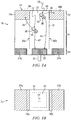
- FIGURES 1A and 1B illustrate various views of an example embodiment of an optical detector 10 with improved quantum efficiency.
- FIGURE 1A illustrates a side view of optical detector 10
- FIGURE 1B illustrates a top view of optical detector 10.
- optical detector 10 includes a detector surface 19, an active pixel area 12, a depleted field region 14, an N+ backside contact region 52, and a P+ implant region 54.
- N+ backside contact region 52 includes N-guard regions 16a and 16b, a doping region 18, and an upper active pixel area 13.
- P+ implant region 54 includes a P-electrode 22, P-guard regions 24a and 24b, and a charge collection node 20, also referred to as a pixel.
- Optical detector 10 may be any type of suitable light detection device, including, but not limited to, a PIN, a PN, an NIP, or an NP diode.
- Optical detector 10 may be constructed of silicon, Gallium Arsenide (GaAs), or any other suitable material.
- GaAs Gallium Arsenide
- optical detector 10 is a PIN diode that includes P+ implant region 54, N+ backside contact region 52 under detector surface 19 and at the opposite end of optical detector 10 from P+ implant region 54, and an intrinsic (or near-intrinsic) material in depleted field region 14 between P+ implant region 54 and N+ backside contact region 52.
- P+ implant region 54 includes P-guard regions 24a and 24b, and a charge collection node 20.
- P-guard regions 24a and 24b and a charge collection node 20 may be any material that has been doped with any suitable P-type doping.
- Charge collection node 20 collect resulting holes from photons that have entered active pixel area 12 through doping region 18 and generates a charge on a P-electrode 22, which is coupled to charge collection node 20.
- P-guard regions 24a and 24b may be used to bias optical detector 10 and to create an electric field, as discussed in more detail below. In particular embodiments, P-guard regions 24a and 24b may not be necessary and therefore may not be implemented.
- N+ backside contact region 52 includes detector surface 19, N-guard regions 16a and 16b, doping region 18, and upper active pixel area 13.
- Upper active pixel area 13 may be any suitable intrinsic (or near-intrinsic) material, such as that utilized in depleted field region 14.
- N-guard regions 16a and 16b may be any material that has been doped with any suitable N-type doping.
- N-guard regions 16a and 16b may be used to collect carriers and prevent crosstalk that may be caused by carriers traveling from one diode to an adjacent diode, as discussed in more detail below. In particular embodiments, N-guard regions 16a and 16b may not be necessary and therefore may not be implemented. In certain embodiments, N-guard regions 16a and 16b may be located adjacent to N electrode 19 and active pixel area 12.
- Optical detector 10 includes depleted field region 14 which lies above charge collection node 20.
- Depleted field region 14 may be any suitable intrinsic (or near-intrinsic) material. In embodiments where doping region 18 has a zero doping concentration, depleted field region 14 extends from charge collection node 20 to detector surface 19 and encompasses upper active pixel area 13. In other embodiments where doping region 18 has a doping concentration greater than zero, depleted field region 14 extends from charge collection node 20 to doping region 18.
- Depleted field region 14 includes active pixel area 12. Active pixel area 12 lies between detector surface 19 and charge collection node 20, and between dashed lines 50a and 50b. In particular embodiments, active pixel area 12 may be other shapes or sizes not specifically shown in the illustrated embodiment.
- Typical optical detectors have regions of high doping that photons must travel through before reaching a detector.
- the entire N+ backside contact region 52 of optical detector 10 (including upper active pixel area 13) would be highly doped with an N-type doping in a typical optical detector. This results in low quantum efficiency in the blue and UV regions since blue and UV light generate hole-electron pairs very near the entrance surface of silicon (i.e., near detector surface 19).
- Optical detector 10 includes upper active pixel area 13, which is a depleted field region, and doping region 18 underlying detector surface 19. This allows optical detector 10 to provide a high quantum efficiency in the blue and UV regions, as explained in more detail below.
- Doping region 18 is a region of optical detector 10 coupled to the underside of detector surface 19.
- doping region 18 may be a region of relatively light doping (i.e., a lighter doping concentration than N-guard regions 16a and 16b).
- doping region 18 may have a light doing concentration of approximately 10 12 atoms/cm 3 .
- doping region 18 may not be doped at all.
- doping region 18 may be a very thin layer of normal doping (i.e., a similar doping concentration to N-guard regions 16a and 16b).
- N-guard regions 16a and 16b may have a thickness that is substantially greater than the thickness of doping region 18.
- doping region 18 has a width that is greater than the width of charge collection node 20.
- photon 26 represents a photon of a relatively longer wavelength, such as 700-900 nanometers.
- Photon 28 represents a photon of a shorter wavelength in the blue and UV regions, such as 300-500 nanometers. Photons of longer wavelength, such as photon 26, tend to penetrate deeper into active pixel area 12 and past N+ backside contact region 52 before they are absorbed and create a hole-electron pair. Photon 26 has created carriers represented by electron 30 and hole 32 in this example. Photons of shorter wavelength, such as photon 28 are absorbed closer to the surface of active pixel area 12, nearer to detector surface 19. Photon 28 has created electron 34 and hole 36 in this example.
- Holes and electrons created by photons entering optical detector 10 may then either recombine (and go undetected) or be swept to a detector or guard region in optical detector 10.
- electrons 30 and 34 may travel to guard regions 16a and 16b, respectively, along paths 38 and 40, respectively.
- Holes 32 and 36 may travel to charge collection node 20 along paths 42 and 44, respectively, where they can be detected by optical detector 10. The detection of the holes by charge collection node 20 may then be used for any suitable purpose.
- the area where shorter wavelength photons create hole-electron pairs is highly doped. In the illustrated embodiment, for example, this would correspond to upper active pixel area 13 and doping region 18.
- a highly doped region has a reduced field and may additionally have damage due to implanting, annealing, and other processing.
- carriers may experience short diffusion lengths and short lifetimes for electron-hole pairs.
- Hole-electron pairs generated in a highly doped and/or damaged region such as those generated from blue and UV light for silicon detectors, may have a higher probability of recombining than pairs generated in an active area outside of the damaged region. As a result, they may not be attracted to opposite electrodes, and may ultimately go undetected. This reduces the quantum efficiency of the device in the short wavelength spectral regions (e.g., blue and UV light).
- Optical detector 10 provides improved quantum efficiency in the short wavelength spectral regions by including a lower, or zero doping level in doping region 18, and an upper active pixel area 13 that is a depleted field region. These regions underlie detector surface 19, as illustrated in optical detector 10 in FIGURE 1 . These regions provide an improved short wave length response for optical detector 10 by reducing the size of the damaged area near detector surface 19, and also providing a field in this region to direct carriers to N-guard regions 16 or charge collection node 20 for detection.
- Optical detector 10 includes guard regions 16a, 16b, 24a, and 24b that maintain the bias on optical detector 10 and prevent crosstalk to adjacent detectors.
- N-guard regions 16a and 16b are adjacent to upper active pixel area 13 and doping region 18 (and underlying detector surface 19) and may be any material that has been doped with any suitable N-type doping to a concentration that is comparatively higher than upper active pixel area 13.
- P-guard regions 24a and 24b may be any material that has been doped with any suitable P-type doping to a concentration that is comparatively higher than depleted field region 14.
- guard regions 16 and 24 may be used to bias optical detector 10 and to create an electric field in depleted field region 14 and upper active pixel area 13. The electric field in these regions may help guide holes and electrons to the detectors.
- guard regions 16 and 24 may be used to collect carriers and prevent crosstalk that may be caused by carriers traveling from one optical detector to an adjacent optical detector. This can also help delineate one optical detector from another.
- guard regions 16 and 24 may not be necessary and therefore may not be implemented.
- N-type doping in regions 16a and 16b, P-type doping in regions 20, 24a, and 24b, and intrinsic or near-intrinsic doping in active pixel area 12 and upper active pixel area 13, the dopants could be reversed in those regions consistent with this discussion.
- N-type dopants include arsenic and phosphorus, among others.
- P-type dopants include boron, among others.
- the width of charge collection node 20 may be selectively controlled to be less than the width of active pixel area 12 between N-guard regions 16a and 16b. This can provide flexibility in fabrication. For example, the width of charge collection node 20 may allow for tolerances when aligning masks for front and/or backside fabrication steps.
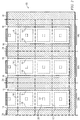
- FIGURE 2 illustrates an example embodiment of an array 60 of multiple optical detectors 10. In this embodiment, parts of twelve optical detectors 10 are illustrated in three columns: columns 64a - 64c. In other embodiments, array 60 may include any number of optical detectors 10 in any number of columns 64. In some embodiments, array 60 may be a focal plane array that includes a detector array of optical detectors 10 and a read-out integrated circuit array (not illustrated in FIGURE 2 ).
- Columns 54a - 64c of array 60 may each correspond to a specific color.
- column 64a may correspond to the color blue and thus may include a corresponding filter (not shown).
- Columns 64b and 64c may correspond to other colors such as red and green and may also include corresponding filters (not shown).
- Each optical detector 10 in array 60 may includes guard regions 16a, 16b, 24a, and 24b, as previously described in reference to FIGURE 1 .
- Guard regions 16 and 24 may help prevent crosstalk between adjacent optical detectors 10 in array 60 and help delineate between optical detectors 10 as previously described.
- optical detector 10 has been described and depicted as a PIN diode. In other embodiments, however, optical detector 10 may be other suitable devices such as a PN, an NIP, or an NP diode.
- dopants arsenic, phosphorus, and boron have been described, any other suitable dopant may be utilized. It is intended that the present disclosure encompass all such changes, substitutions, variations, alterations, and modifications as falling within the spirit and scope of the appended claims.
Landscapes
- Solid State Image Pick-Up Elements (AREA)
- Light Receiving Elements (AREA)
Applications Claiming Priority (4)
| Application Number | Priority Date | Filing Date | Title |
|---|---|---|---|
| US14504109P | 2009-01-15 | 2009-01-15 | |
| US12/611,388 US8294232B2 (en) | 2009-01-15 | 2009-11-03 | High quantum efficiency optical detectors |
| PCT/US2010/021136 WO2010083372A1 (en) | 2009-01-15 | 2010-01-15 | High quantum efficiency optical detectors |
| EP10700789A EP2387802A1 (de) | 2009-01-15 | 2010-01-15 | Optische detektoren mit hohem quantenwirkungsgrad |
Related Parent Applications (1)
| Application Number | Title | Priority Date | Filing Date |
|---|---|---|---|
| EP10700789A Division EP2387802A1 (de) | 2009-01-15 | 2010-01-15 | Optische detektoren mit hohem quantenwirkungsgrad |
Publications (2)
| Publication Number | Publication Date |
|---|---|
| EP3306677A2 true EP3306677A2 (de) | 2018-04-11 |
| EP3306677A3 EP3306677A3 (de) | 2018-07-11 |
Family
ID=42040266
Family Applications (2)
| Application Number | Title | Priority Date | Filing Date |
|---|---|---|---|
| EP10700789A Ceased EP2387802A1 (de) | 2009-01-15 | 2010-01-15 | Optische detektoren mit hohem quantenwirkungsgrad |
| EP17183582.0A Withdrawn EP3306677A3 (de) | 2009-01-15 | 2010-01-15 | Optische detektoren mit hoher quanteneffizienz |
Family Applications Before (1)
| Application Number | Title | Priority Date | Filing Date |
|---|---|---|---|
| EP10700789A Ceased EP2387802A1 (de) | 2009-01-15 | 2010-01-15 | Optische detektoren mit hohem quantenwirkungsgrad |
Country Status (5)
| Country | Link |
|---|---|
| US (1) | US8294232B2 (de) |
| EP (2) | EP2387802A1 (de) |
| IL (1) | IL214020A (de) |
| TW (1) | TWI500180B (de) |
| WO (1) | WO2010083372A1 (de) |
Families Citing this family (1)
| Publication number | Priority date | Publication date | Assignee | Title |
|---|---|---|---|---|
| WO2013095474A1 (en) | 2011-12-21 | 2013-06-27 | Intel Corporation | Methods for forming fins for metal oxide semiconductor device structures |
Family Cites Families (12)
| Publication number | Priority date | Publication date | Assignee | Title |
|---|---|---|---|---|
| EP0778621B1 (de) * | 1995-12-06 | 2008-08-13 | Sony Corporation | Aus einer Fotodiode und einem bipolaren Element bestehende Halbleitervorrichtung und Verfahren zur Herstellung |
| JP3530159B2 (ja) * | 2001-08-22 | 2004-05-24 | 松下電器産業株式会社 | 固体撮像装置およびその製造方法 |
| US6933489B2 (en) | 2002-05-10 | 2005-08-23 | Hamamatsu Photonics K.K. | Back illuminated photodiode array and method of manufacturing the same |
| DE10252878A1 (de) * | 2002-11-12 | 2004-06-03 | X-Fab Semiconductor Foundries Ag | In BiCMOS-Technologie monolithisch integrierte verbesserte vertikale pin-Fotodiode |
| US7462553B2 (en) | 2003-06-25 | 2008-12-09 | Semicoa | Ultra thin back-illuminated photodiode array fabrication methods |
| JP2005317875A (ja) * | 2004-04-30 | 2005-11-10 | Toshiba Corp | 固体撮像装置 |
| KR100760142B1 (ko) * | 2005-07-27 | 2007-09-18 | 매그나칩 반도체 유한회사 | 고해상도 cmos 이미지 센서를 위한 스택형 픽셀 |
| US7683397B2 (en) * | 2006-07-20 | 2010-03-23 | Intel Corporation | Semi-planar avalanche photodiode |
| WO2008058049A2 (en) * | 2006-11-06 | 2008-05-15 | Semequip, Inc. | Ion implantation device and method of semiconductor manufacturing by the implantation of molecular ions containing phosphorus and arsenic |
| TWI479887B (zh) * | 2007-05-24 | 2015-04-01 | 新力股份有限公司 | 背向照明固態成像裝置及照相機 |
| US8558275B2 (en) * | 2007-12-31 | 2013-10-15 | Alpha And Omega Semiconductor Ltd | Sawtooth electric field drift region structure for power semiconductor devices |
| US7732886B2 (en) * | 2008-07-15 | 2010-06-08 | United Microelectronics Corp. | Pin photodiode structure |
-
2009
- 2009-11-03 US US12/611,388 patent/US8294232B2/en active Active
-
2010
- 2010-01-15 TW TW099101058A patent/TWI500180B/zh active
- 2010-01-15 WO PCT/US2010/021136 patent/WO2010083372A1/en not_active Ceased
- 2010-01-15 EP EP10700789A patent/EP2387802A1/de not_active Ceased
- 2010-01-15 EP EP17183582.0A patent/EP3306677A3/de not_active Withdrawn
-
2011
- 2011-07-11 IL IL214020A patent/IL214020A/en active IP Right Grant
Non-Patent Citations (1)
| Title |
|---|
| None |
Also Published As
| Publication number | Publication date |
|---|---|
| US8294232B2 (en) | 2012-10-23 |
| IL214020A (en) | 2017-03-30 |
| EP3306677A3 (de) | 2018-07-11 |
| EP2387802A1 (de) | 2011-11-23 |
| WO2010083372A1 (en) | 2010-07-22 |
| US20110147878A1 (en) | 2011-06-23 |
| TW201031007A (en) | 2010-08-16 |
| TWI500180B (zh) | 2015-09-11 |
| IL214020A0 (en) | 2011-08-31 |
Similar Documents
| Publication | Publication Date | Title |
|---|---|---|
| JP6090060B2 (ja) | シングルフォトンアバランシェダイオード | |
| CN106449770B (zh) | 防止边缘击穿的环形栅单光子雪崩二极管及其制备方法 | |
| JP5942068B2 (ja) | 化合物半導体受光素子アレイ | |
| US9806121B2 (en) | Solid-state imaging device | |
| JP2017005276A (ja) | シングルフォトンアバランシェダイオード | |
| CN114899267A (zh) | 光电转换器件、感测装置、电子设备及制造方法 | |
| US7928533B2 (en) | Nano-multiplication region avalanche photodiodes and arrays | |
| US8212327B2 (en) | High fill-factor laser-treated semiconductor device on bulk material with single side contact scheme | |
| CN107895743B (zh) | 单光子雪崩光电二极管探测器的装置和方法 | |
| US20140159180A1 (en) | Semiconductor resistor structure and semiconductor photomultiplier device | |
| CN117239000B (zh) | 一种雪崩光电二极管及其制作方法、单光子探测器 | |
| US11335825B2 (en) | Single-photon avalanche diode and a sensor array | |
| KR102653478B1 (ko) | 단일 광자 검출 소자, 전자 장치, 및 라이다 장치 | |
| US20060038249A1 (en) | Semiconductor light-receiving device and UV sensor apparatus | |
| US8766339B2 (en) | Highly efficient CMOS technology compatible silicon photoelectric multiplier | |
| CN118748221B (zh) | 电荷耦合型单光子雪崩二极管探测阵列结构及其制备方法 | |
| US8294232B2 (en) | High quantum efficiency optical detectors | |
| US7105906B1 (en) | Photodiode that reduces the effects of surface recombination sites | |
| EP1833095B1 (de) | Photodiode mit verringertem Dunkelstrom | |
| US8513753B1 (en) | Photodiode having a buried well region | |
| US20250366230A1 (en) | Photodetector device having lightly doped layer | |
| US20250248139A1 (en) | Enhanced channel structure for heterojunction semiconductor devices |
Legal Events
| Date | Code | Title | Description |
|---|---|---|---|
| PUAI | Public reference made under article 153(3) epc to a published international application that has entered the european phase |
Free format text: ORIGINAL CODE: 0009012 |
|
| AC | Divisional application: reference to earlier application |
Ref document number: 2387802 Country of ref document: EP Kind code of ref document: P |
|
| AK | Designated contracting states |
Kind code of ref document: A2 Designated state(s): AT BE BG CH CY CZ DE DK EE ES FI FR GB GR HR HU IE IS IT LI LT LU LV MC MK MT NL NO PL PT RO SE SI SK SM TR |
|
| PUAL | Search report despatched |
Free format text: ORIGINAL CODE: 0009013 |
|
| AK | Designated contracting states |
Kind code of ref document: A3 Designated state(s): AT BE BG CH CY CZ DE DK EE ES FI FR GB GR HR HU IE IS IT LI LT LU LV MC MK MT NL NO PL PT RO SE SI SK SM TR |
|
| RIC1 | Information provided on ipc code assigned before grant |
Ipc: H01L 31/075 20120101AFI20180606BHEP Ipc: H01L 27/146 20060101ALI20180606BHEP |
|
| STAA | Information on the status of an ep patent application or granted ep patent |
Free format text: STATUS: THE APPLICATION IS DEEMED TO BE WITHDRAWN |
|
| 18D | Application deemed to be withdrawn |
Effective date: 20190112 |