EP3306655A1 - Substrate for power modules, substrate assembly for power modules, and method for producing substrate for power modules - Google Patents
Substrate for power modules, substrate assembly for power modules, and method for producing substrate for power modules Download PDFInfo
- Publication number
- EP3306655A1 EP3306655A1 EP16800144.4A EP16800144A EP3306655A1 EP 3306655 A1 EP3306655 A1 EP 3306655A1 EP 16800144 A EP16800144 A EP 16800144A EP 3306655 A1 EP3306655 A1 EP 3306655A1
- Authority
- EP
- European Patent Office
- Prior art keywords
- plate
- copper
- power module
- resist film
- etching resist
- Prior art date
- Legal status (The legal status is an assumption and is not a legal conclusion. Google has not performed a legal analysis and makes no representation as to the accuracy of the status listed.)
- Granted
Links
Images



Classifications
-
- H—ELECTRICITY
- H10—SEMICONDUCTOR DEVICES; ELECTRIC SOLID-STATE DEVICES NOT OTHERWISE PROVIDED FOR
- H10W—GENERIC PACKAGES, INTERCONNECTIONS, CONNECTORS OR OTHER CONSTRUCTIONAL DETAILS OF DEVICES COVERED BY CLASS H10
- H10W40/00—Arrangements for thermal protection or thermal control
- H10W40/20—Arrangements for cooling
- H10W40/25—Arrangements for cooling characterised by their materials
- H10W40/255—Arrangements for cooling characterised by their materials having a laminate or multilayered structure, e.g. direct bond copper [DBC] ceramic substrates
-
- B—PERFORMING OPERATIONS; TRANSPORTING
- B32—LAYERED PRODUCTS
- B32B—LAYERED PRODUCTS, i.e. PRODUCTS BUILT-UP OF STRATA OF FLAT OR NON-FLAT, e.g. CELLULAR OR HONEYCOMB, FORM
- B32B15/00—Layered products comprising a layer of metal
- B32B15/04—Layered products comprising a layer of metal comprising metal as the main or only constituent of a layer, which is next to another layer of the same or of a different material
-
- B—PERFORMING OPERATIONS; TRANSPORTING
- B32—LAYERED PRODUCTS
- B32B—LAYERED PRODUCTS, i.e. PRODUCTS BUILT-UP OF STRATA OF FLAT OR NON-FLAT, e.g. CELLULAR OR HONEYCOMB, FORM
- B32B15/00—Layered products comprising a layer of metal
- B32B15/20—Layered products comprising a layer of metal comprising aluminium or copper
-
- B—PERFORMING OPERATIONS; TRANSPORTING
- B32—LAYERED PRODUCTS
- B32B—LAYERED PRODUCTS, i.e. PRODUCTS BUILT-UP OF STRATA OF FLAT OR NON-FLAT, e.g. CELLULAR OR HONEYCOMB, FORM
- B32B18/00—Layered products essentially comprising ceramics, e.g. refractory products
-
- B—PERFORMING OPERATIONS; TRANSPORTING
- B32—LAYERED PRODUCTS
- B32B—LAYERED PRODUCTS, i.e. PRODUCTS BUILT-UP OF STRATA OF FLAT OR NON-FLAT, e.g. CELLULAR OR HONEYCOMB, FORM
- B32B3/00—Layered products comprising a layer with external or internal discontinuities or unevennesses, or a layer of non-planar shape; Layered products comprising a layer having particular features of form
- B32B3/26—Layered products comprising a layer with external or internal discontinuities or unevennesses, or a layer of non-planar shape; Layered products comprising a layer having particular features of form characterised by a particular shape of the outline of the cross-section of a continuous layer; characterised by a layer with cavities or internal voids ; characterised by an apertured layer
- B32B3/263—Layered products comprising a layer with external or internal discontinuities or unevennesses, or a layer of non-planar shape; Layered products comprising a layer having particular features of form characterised by a particular shape of the outline of the cross-section of a continuous layer; characterised by a layer with cavities or internal voids ; characterised by an apertured layer characterised by a layer having non-uniform thickness
-
- B—PERFORMING OPERATIONS; TRANSPORTING
- B32—LAYERED PRODUCTS
- B32B—LAYERED PRODUCTS, i.e. PRODUCTS BUILT-UP OF STRATA OF FLAT OR NON-FLAT, e.g. CELLULAR OR HONEYCOMB, FORM
- B32B3/00—Layered products comprising a layer with external or internal discontinuities or unevennesses, or a layer of non-planar shape; Layered products comprising a layer having particular features of form
- B32B3/26—Layered products comprising a layer with external or internal discontinuities or unevennesses, or a layer of non-planar shape; Layered products comprising a layer having particular features of form characterised by a particular shape of the outline of the cross-section of a continuous layer; characterised by a layer with cavities or internal voids ; characterised by an apertured layer
- B32B3/30—Layered products comprising a layer with external or internal discontinuities or unevennesses, or a layer of non-planar shape; Layered products comprising a layer having particular features of form characterised by a particular shape of the outline of the cross-section of a continuous layer; characterised by a layer with cavities or internal voids ; characterised by an apertured layer characterised by a layer formed with recesses or projections, e.g. hollows, grooves, protuberances, ribs
-
- B—PERFORMING OPERATIONS; TRANSPORTING
- B32—LAYERED PRODUCTS
- B32B—LAYERED PRODUCTS, i.e. PRODUCTS BUILT-UP OF STRATA OF FLAT OR NON-FLAT, e.g. CELLULAR OR HONEYCOMB, FORM
- B32B37/00—Methods or apparatus for laminating, e.g. by curing or by ultrasonic bonding
- B32B37/06—Methods or apparatus for laminating, e.g. by curing or by ultrasonic bonding characterised by the heating method
-
- B—PERFORMING OPERATIONS; TRANSPORTING
- B32—LAYERED PRODUCTS
- B32B—LAYERED PRODUCTS, i.e. PRODUCTS BUILT-UP OF STRATA OF FLAT OR NON-FLAT, e.g. CELLULAR OR HONEYCOMB, FORM
- B32B7/00—Layered products characterised by the relation between layers; Layered products characterised by the relative orientation of features between layers, or by the relative values of a measurable parameter between layers, i.e. products comprising layers having different physical, chemical or physicochemical properties; Layered products characterised by the interconnection of layers
- B32B7/04—Interconnection of layers
-
- B—PERFORMING OPERATIONS; TRANSPORTING
- B32—LAYERED PRODUCTS
- B32B—LAYERED PRODUCTS, i.e. PRODUCTS BUILT-UP OF STRATA OF FLAT OR NON-FLAT, e.g. CELLULAR OR HONEYCOMB, FORM
- B32B7/00—Layered products characterised by the relation between layers; Layered products characterised by the relative orientation of features between layers, or by the relative values of a measurable parameter between layers, i.e. products comprising layers having different physical, chemical or physicochemical properties; Layered products characterised by the interconnection of layers
- B32B7/04—Interconnection of layers
- B32B7/08—Interconnection of layers by mechanical means
-
- B—PERFORMING OPERATIONS; TRANSPORTING
- B32—LAYERED PRODUCTS
- B32B—LAYERED PRODUCTS, i.e. PRODUCTS BUILT-UP OF STRATA OF FLAT OR NON-FLAT, e.g. CELLULAR OR HONEYCOMB, FORM
- B32B9/00—Layered products comprising a layer of a particular substance not covered by groups B32B11/00 - B32B29/00
- B32B9/005—Layered products comprising a layer of a particular substance not covered by groups B32B11/00 - B32B29/00 comprising one layer of ceramic material, e.g. porcelain, ceramic tile
-
- B—PERFORMING OPERATIONS; TRANSPORTING
- B32—LAYERED PRODUCTS
- B32B—LAYERED PRODUCTS, i.e. PRODUCTS BUILT-UP OF STRATA OF FLAT OR NON-FLAT, e.g. CELLULAR OR HONEYCOMB, FORM
- B32B9/00—Layered products comprising a layer of a particular substance not covered by groups B32B11/00 - B32B29/00
- B32B9/04—Layered products comprising a layer of a particular substance not covered by groups B32B11/00 - B32B29/00 comprising such particular substance as the main or only constituent of a layer, which is next to another layer of the same or of a different material
- B32B9/041—Layered products comprising a layer of a particular substance not covered by groups B32B11/00 - B32B29/00 comprising such particular substance as the main or only constituent of a layer, which is next to another layer of the same or of a different material of metal
-
- H—ELECTRICITY
- H10—SEMICONDUCTOR DEVICES; ELECTRIC SOLID-STATE DEVICES NOT OTHERWISE PROVIDED FOR
- H10W—GENERIC PACKAGES, INTERCONNECTIONS, CONNECTORS OR OTHER CONSTRUCTIONAL DETAILS OF DEVICES COVERED BY CLASS H10
- H10W70/00—Package substrates; Interposers; Redistribution layers [RDL]
- H10W70/01—Manufacture or treatment
- H10W70/02—Manufacture or treatment of conductive package substrates serving as an interconnection, e.g. of metal plates
-
- B—PERFORMING OPERATIONS; TRANSPORTING
- B32—LAYERED PRODUCTS
- B32B—LAYERED PRODUCTS, i.e. PRODUCTS BUILT-UP OF STRATA OF FLAT OR NON-FLAT, e.g. CELLULAR OR HONEYCOMB, FORM
- B32B2250/00—Layers arrangement
- B32B2250/40—Symmetrical or sandwich layers, e.g. ABA, ABCBA, ABCCBA
-
- B—PERFORMING OPERATIONS; TRANSPORTING
- B32—LAYERED PRODUCTS
- B32B—LAYERED PRODUCTS, i.e. PRODUCTS BUILT-UP OF STRATA OF FLAT OR NON-FLAT, e.g. CELLULAR OR HONEYCOMB, FORM
- B32B2307/00—Properties of the layers or laminate
- B32B2307/20—Properties of the layers or laminate having particular electrical or magnetic properties, e.g. piezoelectric
- B32B2307/202—Conductive
-
- B—PERFORMING OPERATIONS; TRANSPORTING
- B32—LAYERED PRODUCTS
- B32B—LAYERED PRODUCTS, i.e. PRODUCTS BUILT-UP OF STRATA OF FLAT OR NON-FLAT, e.g. CELLULAR OR HONEYCOMB, FORM
- B32B2307/00—Properties of the layers or laminate
- B32B2307/30—Properties of the layers or laminate having particular thermal properties
- B32B2307/302—Conductive
-
- B—PERFORMING OPERATIONS; TRANSPORTING
- B32—LAYERED PRODUCTS
- B32B—LAYERED PRODUCTS, i.e. PRODUCTS BUILT-UP OF STRATA OF FLAT OR NON-FLAT, e.g. CELLULAR OR HONEYCOMB, FORM
- B32B2307/00—Properties of the layers or laminate
- B32B2307/70—Other properties
- B32B2307/732—Dimensional properties
-
- B—PERFORMING OPERATIONS; TRANSPORTING
- B32—LAYERED PRODUCTS
- B32B—LAYERED PRODUCTS, i.e. PRODUCTS BUILT-UP OF STRATA OF FLAT OR NON-FLAT, e.g. CELLULAR OR HONEYCOMB, FORM
- B32B2311/00—Metals, their alloys or their compounds
- B32B2311/12—Copper
-
- B—PERFORMING OPERATIONS; TRANSPORTING
- B32—LAYERED PRODUCTS
- B32B—LAYERED PRODUCTS, i.e. PRODUCTS BUILT-UP OF STRATA OF FLAT OR NON-FLAT, e.g. CELLULAR OR HONEYCOMB, FORM
- B32B2315/00—Other materials containing non-metallic inorganic compounds not provided for in groups B32B2311/00 - B32B2313/04
- B32B2315/02—Ceramics
-
- B—PERFORMING OPERATIONS; TRANSPORTING
- B32—LAYERED PRODUCTS
- B32B—LAYERED PRODUCTS, i.e. PRODUCTS BUILT-UP OF STRATA OF FLAT OR NON-FLAT, e.g. CELLULAR OR HONEYCOMB, FORM
- B32B2457/00—Electrical equipment
-
- H—ELECTRICITY
- H10—SEMICONDUCTOR DEVICES; ELECTRIC SOLID-STATE DEVICES NOT OTHERWISE PROVIDED FOR
- H10W—GENERIC PACKAGES, INTERCONNECTIONS, CONNECTORS OR OTHER CONSTRUCTIONAL DETAILS OF DEVICES COVERED BY CLASS H10
- H10W70/00—Package substrates; Interposers; Redistribution layers [RDL]
- H10W70/60—Insulating or insulated package substrates; Interposers; Redistribution layers
- H10W70/67—Insulating or insulated package substrates; Interposers; Redistribution layers characterised by their insulating layers or insulating parts
- H10W70/68—Shapes or dispositions thereof
-
- H—ELECTRICITY
- H10—SEMICONDUCTOR DEVICES; ELECTRIC SOLID-STATE DEVICES NOT OTHERWISE PROVIDED FOR
- H10W—GENERIC PACKAGES, INTERCONNECTIONS, CONNECTORS OR OTHER CONSTRUCTIONAL DETAILS OF DEVICES COVERED BY CLASS H10
- H10W70/00—Package substrates; Interposers; Redistribution layers [RDL]
- H10W70/60—Insulating or insulated package substrates; Interposers; Redistribution layers
- H10W70/67—Insulating or insulated package substrates; Interposers; Redistribution layers characterised by their insulating layers or insulating parts
- H10W70/68—Shapes or dispositions thereof
- H10W70/6875—Shapes or dispositions thereof being on a metallic substrate, e.g. insulated metal substrates [IMS]
Definitions
- the present invention relates to a power module substrate, including a ceramic plate and a copper plate joined together for mainly mounting a power semiconductor device, and a collective substrate for power modules, and a method for manufacturing the power module substrate.
- a substrate for a power module includes a ceramic plate, an island-shaped copper circuit plate arranged on one main surface of the ceramic plate, and a heat dissipation copper plate arranged on the other main surface of the ceramic plate.
- This power module substrate is used for mounting a power semiconductor device, such as a power integrated circuit (IC) or an insulated gate bipolar transistor (IGBT), or for mounting a passive device, such as a capacitor.
- IC power integrated circuit
- IGBT insulated gate bipolar transistor
- Recent power semiconductor devices consume more power, and generate more heat.
- Substrates for power modules may thus need to have higher heat resistance, heat dissipation, and insulation.
- a power module substrate includes a ceramic plate to increase heat resistance and insulation.
- a power module substrate may also include a joined structure of a copper plate and a ceramic plate to increase heat dissipation.
- a power module substrate is typically designed to dissipate heat generated from a semiconductor device mounted on its copper circuit plate downward through the copper circuit plate, a ceramic plate, and a heat dissipation copper plate.
- the power module substrate including the joined structure of the ceramic plate and the copper plate can have issues including lower heat dissipation through the ceramic plate with low heat conductivity, and separation of the edges of the copper plate from the ceramic plate or cracks in the ceramic plate under heat stress at the joint interface between the ceramic plate and the copper plates resulting from the different thermal expansion coefficients of ceramics and copper.
- a power module substrate may include, for example, a ceramic plate formed from a highly conductive ceramic, such as aluminum nitride.
- the ceramic plate formed from aluminum nitride is very expensive.
- the power module substrate may include a thinner ceramic plate.
- the thinner ceramic plate formed from an alumina-based ceramic can have a lower strength.
- a silicon nitride-based ceramic, which has high strength, may be used.
- the ceramic plate formed from silicon nitride is very expensive.
- the power module substrate may include a thicker copper plate joined with a ceramic plate.
- the increased heat stress at the joint interface between the ceramic plate and the copper plates resulting from the different thermal expansion coefficients of ceramics and copper may cause separation of the edges of the copper plate and cracks in the ceramic plate.
- a thin ceramic plate with high heat dissipation made of zirconia added alumina having higher strength than ceramics made of alumina is available recently.
- This ceramic plate joined with a relatively thick copper plate intends to reduce separation of the edges of the copper plate and to minimize cracks in the ceramic plate under heat stress at the joint interface between the ceramic plate and the copper plate resulting from the different thermal expansion coefficients of ceramics and copper.
- the joined structure of the ceramic plate and the copper plates is typically prepared by brazing the copper plates on the two main surfaces of the ceramic plate using an active metal brazing material, or by direct copper bonding (DCB) using heat, which directly bonds the ceramic plate and the copper plates with heat.
- Brazing using the active metal brazing material allows an active metal brazing material layer, such as a Ag/Cu/Ti layer, to form between the ceramic plate and the copper plates.
- the brazing layer is expected to serve as a buffer layer against heat stress.
- the active metal brazing material layer can slightly degrade heat dissipation.
- the DCB using heat is suited for bonding an oxide ceramic plate of, for example, alumina with copper plates.
- the power module substrate prepared by the DCB using heat includes the copper plates and the ceramic plate joined either directly, or with a very thin copper oxide layer between them, and thus has high heat transfer, or high heat dissipation, at the interfaces between the ceramic plate and the copper plates.
- the ceramic plate or the copper plates still need some measures to reduce stress at the joint interfaces between the ceramic plate and the copper plate edges.
- the joined structure of the ceramic plate and the copper plates can have its copper plate surface masked using an etching resist having an intended pattern.
- the uncovered portions of the copper plate may then be removed by chemical corrosion (etching) to yield the copper circuit plate with an intended shape.
- the power module substrate is typically obtained from a collective substrate including a plurality of areas to be a plurality of power module substrates, which are then cut along the splitting grooves formed along the boundaries of the power module substrates.
- a power module substrate known in the art may have its copper plate with protrusions and recesses on the surface to reduce stress at the joint interface between a ceramic plate and the edges of the copper plate, to position a semiconductor device for soldering, or to prevent overflow of solder (refer to, for example, Patent Literatures 1, 2, and 3).
- a method for manufacturing a power module substrate known in the art may form a metal circuit pattern through the three processes: (1) half-etching a metal plate into the shape of a circuit pattern, (2) joining the etched surface with a ceramic plate, and (3) applying an etching resist on the surface of the metal plate that is not joined with the ceramic plate, and half-etching the plate to form a step (refer to, for example, Patent Literature 4).
- the etching resist film is formed by applying a known ultraviolet curable or thermosetting resist paste onto the metal plate by screen printing, and then curing the paste.
- the power module substrate and the method for manufacturing the power module substrate can have issues described below.
- the thickness of the copper plate as a mount for the semiconductor device may be increased to increase the range of heat transfer and diffusion toward the ceramic plate.
- increasing the thickness of the semiconductor device mounting area of the copper plate increases the thickness of the entire island-shaped copper circuit plate. This increases heat stress at the joint interface of the ceramic plate and the copper plate resulting from the different thermal expansion coefficients of ceramics and copper.
- the thinner copper plate disables prompt heat dissipation from the semiconductor device.
- the power module substrates described in Japanese Unexamined Patent Application Publication Nos. 4-103150 , 10-242330 , and 10-242331 each include a copper circuit plate having surface protrusions and recesses, on which a semiconductor device is soldered in a recess, and thus prevent overflow of the solder.
- the portion on which the semiconductor device is mounted has the same thickness as or is thinner than its surrounding portions.
- this structure may not promptly dissipate heat generated from the semiconductor device, and may not reduce heat stress at the joint interface between the ceramic plate and the copper plate resulting from the different thermal expansion coefficients of ceramics and copper and may not prevent separation of the copper plate edges from the ceramic plate and cracks in the ceramic plate.
- the copper plate is then half-etched into the shape of an intended circuit pattern before it is joined to the ceramic plate. This may involve misalignment between the copper circuit plate and the ceramic plate. Particularly when individual power module substrates are formed from a large ceramic plate including a plurality of areas to be the substrates, such misalignment can cause relative misalignment of all the copper circuit plates to be joined onto the large ceramic plate. This lowers the yield.
- one aspect of the present invention provides a substrate for a power module that allows prompt heat dissipation from a semiconductor device, and avoid separation of the edges of a copper plate from a ceramic plate and cracks in the ceramic plate under heat stress at the joint interface of the ceramic plate and the copper plate resulting from the different thermal expansion coefficients of ceramics and copper.
- Another aspect of the present invention provides a method for manufacturing a substrate for a power module including a copper circuit plate with precise protrusions and recesses capable of promptly dissipating heat generated from a semiconductor device and reducing heat stress at the joint interface between a ceramic plate and the copper plate resulting from the different thermal expansion coefficients of ceramics and copper.
- Another aspect of the present invention provides a method for manufacturing a substrate for a power module for forming a copper circuit plate with precise protrusions and recesses including a portion for preventing overflow of solder when a semiconductor device is joined with solder.
- a first aspect of the present invention provides a substrate for a power module including a ceramic plate, a copper circuit plate on a main surface of the ceramic plate, and a heat dissipation copper plate on a surface of the ceramic plate opposite to the main surface.
- the copper circuit plate includes at least one first copper circuit plate, and at least one second copper circuit plate different from the first copper circuit plate.
- the first copper circuit plate includes a first portion on which a semiconductor device is mountable, and a second portion having a smaller thickness than the first portion. The second portion is outward from and surrounding the first portion.
- a second aspect of the present invention may provide the substrate for a power module according to the first aspect, in which the first copper circuit plate further includes a third portion between the first portion and the second portion, and the third portion has a smaller thickness than the second portion.
- a third aspect of the present invention may provide the substrate for a power module according to the first aspect or the second aspect, in which the second copper circuit plate has a smaller thickness than the first portion.
- a fourth aspect of the present invention may provide a collective substrate for power modules, in which the collective substrate includes a plurality of the substrates for a power module according to any one of the first to third aspects that are arranged in a matrix and are integral with one another.
- a fifth aspect of the present invention provides a method for manufacturing a substrate for a power module.
- the method includes joining a first large copper plate, and a second large copper plate on two surfaces of a ceramic plate by direct copper bonding using heat or brazing using an active metal brazing material, forming a first etching resist film on each of the first and second large copper plates, etching a portion of each of the first and second large copper plates without the first etching resist film to reduce a thickness of the portion, removing the first etching resist film, forming a second etching resist film on the first large copper plate and a third etching resist film on the second large copper plate, etching a portion of each of the first and second large copper plates without the second etching resist film and the third etching resist film to expose the ceramic plate, removing the second etching resist film, removing the third etching resist film, and forming laser scribe lines for cutting on a surface of the ceramic plate.
- the second etching resist film is formed with an in
- the method according to the fifth aspect for manufacturing a substrate for a power module may further include, between the removing the second etching resist film and the removing the third etching resist film, forming a fourth etching resist film with an inkjet method on the first large copper plate from which the second etching resist film has been removed, and etching a portion of the first large copper plate without the fourth etching resist film to reduce a thickness of the portion to be smaller than a thickness of the etched portion of each of the first and second large copper plates without the first etching resist film.
- the power module substrate includes the copper circuit plate including the first copper circuit plate and the second copper circuit plate different from the first copper circuit plate.
- the first copper circuit plate includes the first portion on which a semiconductor device is mountable, and the second portion having a smaller thickness than the first portion.
- the second portion is outward from and surrounds the first portion.
- the thickness of the first portion of the copper circuit plate, on which a semiconductor device is mountable, can thus be increased. This structure can increase the range of heat transfer and diffusion from the first portion, and allows heat generated from the semiconductor device to be promptly transferred to the heat dissipation copper plate arranged under the ceramic plate.
- the second portion of the copper circuit plate has a smaller thickness than the first portion of the copper circuit plate, and thus can reduce heat stress at the joint interface between the ceramic plate and the copper plate resulting from the different thermal expansion coefficients of ceramics and copper. This structure avoids separation of the edges of the copper circuit plate from the ceramic plate, and cracks in the ceramic plate.
- the power module substrate according to the second aspect of the present invention includes the third portion surrounding the first portion.
- the third portion has a smaller thickness than the second portion.
- the power module substrate according to the third aspect of the present invention includes the second copper circuit plate having a smaller thickness than the first portion of the copper circuit plate, and thus can reduce heat stress at the joint interface between the ceramic plate and the second copper circuit plate resulting from the different thermal expansion coefficients of ceramics and copper. This structure avoids separation of the edges of the second copper circuit plate from the ceramic plate, and cracks in the ceramic plate.
- the bond that can overflow from the first portion when a semiconductor device is joined to the first portion with a bond is blocked by the step formed between the second portion and the third portion. This prevents a short circuit between the first copper circuit plate and the second copper circuit plate.
- the collective substrate for power modules according to the fourth aspect of the present invention includes first portions that are arranged regularly for mounting semiconductor devices. This allows semiconductor devices to be efficiently mounted onto the first portions.
- the collective substrate for power modules according to the fourth aspect of the present invention increases the productivity of the final products.
- the method for manufacturing a substrate for a power module according to the fifth aspect of the present invention is a method for manufacturing the power module substrate according to the first aspect of the present invention and the power module substrate according to the fourth aspect of the present invention.
- the method according to the fifth aspect enables manufacture of the power module substrate that promptly dissipates heat generated from the semiconductor device, and reduces heat stress at the joint interface between the ceramic plate and the copper plate resulting from the different thermal expansion coefficients of ceramics and copper to avoid separation of the edges of the copper circuit plate from the ceramic plate and cracks in the ceramic plate in the resultant power module substrate.
- the method for manufacturing a substrate for a power module according to the fifth aspect of the present invention uses an inkjet method to form the second etching resist film.
- the resultant second etching resist film can have a cross-section in correspondence with any protrusions and recesses formed on the large copper plate surface.
- the second etching resist film can be formed at intended positions with high accuracy on the large copper plate with surface protrusions and recesses. This method easily forms the second etching resist film without rupture or breaks on any surface protrusions and recesses of the large copper plate. The subsequent etching thus forms precise protrusions and recesses on the large copper plate.
- the method for manufacturing a substrate for a power module according to the sixth aspect of the present invention uses an inkjet method to form the fourth etching resist film.
- the resultant fourth etching resist film can have a cross-section in correspondence with any protrusions and recesses formed on the large copper plate surface.
- the fourth etching resist film can be formed at intended positions with high accuracy on the large copper plate with surface protrusions and recesses.
- the method forms the fourth etching resist film without rupture or breaks on any surface protrusions and recesses of the large copper plate. The subsequent etching thus forms precise protrusions and recesses on the large copper plate.
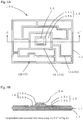
- a substrate for a power module according to one embodiment of the present invention will now be described with reference to Figs. 1A and 1B .
- a substrate 10 for a power module includes a ceramic plate 11, and an island-shaped copper circuit plate 12, which is joined to one main surface of the ceramic plate 11.
- the entire circuit substrate 12 forms an electric circuit.
- the power module substrate 10 further includes a heat dissipation copper plate 13, which is joined to the other main surface of the ceramic plate 11 to cover the entire surface of the other main surface (where the term entire includes substantially entire).
- the heat dissipation copper plate 13 dissipates heat generated from an electronic component (e.g., a semiconductor device 14) mounted on the copper circuit plate 12 downward (toward the other main surface).
- the copper circuit plate 12 includes a first copper circuit plate 12a for mounting the electronic component, such as the semiconductor device 14, and second copper circuit plates 12b different from the first copper circuit plate 12a.
- first copper circuit plate 12a is arranged on one main surface of the ceramic plate 11 in the present embodiment, two or more first copper circuit plates 12a may be arranged on one main surface of the ceramic plate 11.
- the multiple second copper circuit plates 12b are arranged on one main surface of the ceramic plate 11 in the present embodiment, a single second copper circuit plate 12b may be arranged on the surface.
- the semiconductor device 14 is mounted on the first copper circuit plate 12a as one example of an electronic component in Figs. 1 to 5 for easy understanding of the advantageous effects of the power module substrate according to the present embodiment, the electronic component, such as the semiconductor device 14, may not be an element to be included in the claimed invention.
- the power module substrate 10 has an electronic component, such as the semiconductor device 14, joined to each of the first copper circuit plates 12a with a bond, such as solder.
- a connecting terminal mounted on the upper surface of the semiconductor device 14 is electrically connected to the second copper circuit plate 12b with a bonding wire (not shown), and the second copper circuit plate 12b is electrically connected to an external circuit with a metal lead.
- the power module substrate 10 promptly transfers heat generated from the power semiconductor device 14, such as a power integrated circuit (IC) or an insulated gate bipolar transistor (IGBT), downward through the copper circuit plate 12 to the heat dissipation copper plate 13 (on the other main surface of the ceramic plate 11), and further to a fin heatsink or water cooling heatsink (not shown), which is attached to the heat dissipation copper plate 13.
- the power semiconductor device 14 such as a power integrated circuit (IC) or an insulated gate bipolar transistor (IGBT)
- IC power integrated circuit
- IGBT insulated gate bipolar transistor
- the thickness of the copper plates (the copper circuit plate 12 and the heat dissipation copper plate 13) largely affects any improvement in the heat dissipation of the power module substrate 10.
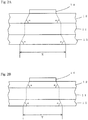
- the heat dissipation that can differ depending on the thickness of the copper plates (the first copper circuit plate 12a) will now be described with reference to Figs. 2A and 2B .
- Heat generated from the semiconductor device 14 mounted on the copper circuit plate 12 (first copper circuit plate 12a) is promptly transferred from the upper surface toward the lower surface of the copper circuit plate 12, which has high heat conductivity, while spreading downward at a substantially constant angle ⁇ .
- the heat reaching the lower surface of the copper circuit plate 12 is then transferred substantially at right angles from the upper surface toward the lower surface of the ceramic plate 11.
- the heat reaching the lower surface of the ceramic plate 11 is promptly transferred from the upper surface toward the lower surface of the heat dissipation copper plate 13, which has high heat conductivity, while diverging downward at a substantially constant angle ⁇ .
- the heat reaching the lower surface of the heat dissipation copper plate 13 is then directed outside by air cooling using, for example, heat radiating fins or a heatsink plate (not shown), or by water cooling (not shown) using circulating water along the surface of the heat dissipation copper plate 13.
- X is the transfer range of heat reaching the lower surface of the heat dissipation copper plate 13 in the structure including a thick copper circuit plate 12 and a thick heat dissipation copper plate 13.
- Y is the transfer range of heat reaching the lower surface of the heat dissipation copper plate 13 in the structure including a thin copper circuit plate 12 and a thin heat dissipation copper plate 13.
- X > Y
- the heat dissipation is thus higher as the copper plates (the copper circuit plate 12 and the heat dissipation copper plate 13) are thicker, and is lower as the copper plates (the copper circuit plate 12 and the heat dissipation copper plate 13) are thinner.
- the temperature at which the copper circuit plate 12 or the heat dissipation copper plate 13 is joined to the ceramic plate 11 typically reaches 800 °C or higher, or can reach 1000 °C or higher. This temperature is far higher than the temperature at which resin and copper for a plastic circuit substrate are joined together in the process of manufacturing the plastic circuit substrate.
- the use of a thicker copper circuit plate 12 and a thicker heat dissipation copper plate 13 joined to the ceramic plate 11 to increase heat dissipation in the power module substrate 10 undergoing such manufacturing processes can cause separation of the edges of the copper circuit plate 12 and the heat dissipation copper plate 13 from the ceramic plate 11 or can cause cracks in the ceramic plate 11 under heat stress resulting from the different thermal expansion coefficients of ceramics and copper at the joint interfaces of the ceramic plate 11 and the copper plates (the copper circuit plate 12 and the heat dissipation copper plate 13).
- the copper circuit plate 12 and the heat dissipation copper plate 13 When the copper circuit plate 12 and the heat dissipation copper plate 13 are joined to the ceramic plate 11, the copper circuit plate 12 and the heat dissipation copper plate 13 can undergo distortion caused by the different thermal expansion coefficients of ceramics and copper. When such distortion occurs unevenly across the copper circuit plate 12 and the heat dissipation copper plate 13, the power module substrate can warp. To reduce such warpage of the power module substrate, the thicknesses of the copper circuit plate 12 and the heat dissipation copper plate 13 are to be adjusted to allow the copper circuit plate 12 and the heat dissipation copper plate 13 to have substantially the same volume.
- the power module substrate 10 includes the first copper circuit plate 12a, on which the semiconductor device 14 is to be mounted.
- the first copper circuit plate 12a has an area 15 including portions with varying thicknesses depending on their use in the copper circuit plate 12.
- the area 15 includes a first portion 15a with the largest thickness, and a second portion 15b with a smaller thickness than the first portion 15a.
- the second portion 15b is outward from the first portion 15a, and surrounds the first portion 15a.
- the power module substrate 10 according to the present embodiment has an electronic component (e.g., the semiconductor device 14) joined to the thickest first portion 15a with a bond (e.g., solder).
- the power module substrate 10 allows the semiconductor device 14 to be mounted on the thickest first portion 15a in the first copper circuit plate 12a, and thus can promptly transmit heat generated from the semiconductor device 14 toward the lower surface (toward the other main surface), while increasing the range of heat transfer and diffusion downward at a substantially constant angle ⁇ . Further, heat generated from the semiconductor device 14 can be promptly transferred though the heat dissipation copper plate 13 arranged under the ceramic plate 11 toward the lower surface, while increasing the range of heat transfer and diffusion downward at a substantially constant angle ⁇ . This allows heat generated from the semiconductor device 14 to be efficiently dissipated outside through a heatsink (not shown) joined to the heat dissipation copper plate 13.
- the second portion 15b of the first copper circuit plate 12a has a smaller thickness than the first portion 15a of the first copper circuit plate 12a, and thus can reduce heat stress resulting from the different thermal expansion coefficients of ceramics and copper at the joint interface between the ceramic plate 11 and the second copper circuit plate 12b. This structure avoids separation of the edges of the copper plate 12 from the ceramic plate 11, and cracks in the ceramic plate 11.
- the heat dissipation copper plate 13 arranged on the lower surface of the ceramic plate 11 may have a thickness falling between the thickness of the first portion 15a and the thickness of the second portion 15b.
- the thickness of the second copper circuit plate 12b greater than the thickness of the first portion 15a increases heat stress at the joint interface between the ceramic plate 11 and the second copper circuit plate 12b resulting from the different thermal expansion coefficients of ceramics and copper.
- the resultant structure may not easily avoid separation of the edges of the second copper circuit plate 12b from the ceramic plate 11 or fracture caused by cracks in the ceramic plate 11.
- the ceramic plate 11 for the power module substrate 10 may be formed from an oxide of mainly alumina, such as alumina or alumina-zirconia, or may be formed from silicon nitride or aluminum nitride. These ceramics may not have a purity of 100%, and may contain 5% or less by weight of other components that aids sintering of ceramics, such as silicon, magnesium, or a rare earth element.
- the ceramic plate 11 for the power module substrate 10 typically has a thickness in the range of 0.2 to 1.0 mm, the ceramic plate 11 is to be thinner to increase heat dissipation unless the strength and the insulation of the ceramic plate 11 are degraded.
- an alumina-based oxide ceramic including, for example, alumina or alumina-zirconia, may be used as the ceramic plate 11.
- a nitride ceramic such as silicon nitride or aluminum nitride containing 5% or less by weight of other components such as silicon, magnesium, or a rare earth element, may also be used.
- the copper circuit plate 12 and the heat dissipation copper plate 13 can be joined to the ceramic plate 11 by brazing using an active metal brazing material.
- the material for the copper circuit plate 12 and the heat dissipation copper plate 13 for the power module substrate 10 may be oxygen-free copper, tough pitch copper, or phosphorus deoxidized copper, which has high electrical conductivity and thermal conductivity, and is inexpensive.
- the copper circuit plate 12 and the heat dissipation copper plate 13 may contain impurities unless such impurities affect the characteristics of the material microstructure.
- the permissive amount of impurities for example, silver or tin, is up to 0.05% by weight.
- the thickness of the copper circuit plate 12 and the heat dissipation copper plate 13 for the power module substrate 10 is typically in the range of 0.2 to 0.6 mm, the thickness may be 1.0 mm or more for use that needs heat dissipation.
- Patent Literature 3 Japanese Unexamined Patent Application Publication No. 10-242331 ) describes, as shown in Figs. 2 and 3 of the literature, a technique for forming a ridge surrounding the semiconductor device on the surface of the copper circuit plate to prevent overflow of the solder.
- the ridge prevents overflow of solder for joining the semiconductor device to the copper circuit plate.
- this technique includes no consideration for heat dissipation from the semiconductor device.
- the circuit plate (2) on the lower surface of the semiconductor device has a uniform thickness. Increasing the thickness of the circuit plate (2) to improve heat dissipation would cause the edges of the circuit plate (2) to easily separate from the ceramic substrate (1). In contrast, decreasing the thickness of the circuit plate (2) to prevent separation of the edges of the circuit plate (2) from the ceramic substrate (1) can lower the dissipation of heat generated from the semiconductor device.
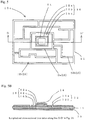
- a power module 10a includes an island-shaped copper circuit plate 12, which includes a first copper circuit plate 12a and a second copper circuit plate 12b on one main surface of the ceramic plate 11, and a heat dissipation copper plate 13 on the other main surface of the ceramic plate 11.
- the first copper circuit plate 12a on which a semiconductor device 14 is to be mounted, has an area 15 including portions with varying thicknesses depending on their use. More specifically, as shown in Figs. 3A and 3B , the area 15 includes a third portion 15c between a first portion 15a and a second portion 15b included in the copper circuit plate 12.
- the third portion 15c has a smaller thickness than the second portion 15b.
- the copper circuit plate 12 is thinner in the order of the first portion 15a, the second portion 15b, and the third portion 15c of the area 15.
- the power module substrate 10a shown in Figs. 3A and 3B may include the second copper circuit plate 12b with any thickness.
- the second copper circuit plate 12b thicker than the first portion 15a increases heat stress at the joint interface between the ceramic plate 11 and the second copper circuit plate 12b resulting from the different thermal expansion coefficients of ceramics and copper.
- the thickness of the second copper circuit plate 12b is to be smaller than the thickness of the first portion 15a in the power module substrate 10a according to the modification of the present invention as well.
- the power module substrate 10a according to the modification of the present invention can promptly dissipate heat generated from the semiconductor device 14, and can avoid separation of the edges of the copper circuit plate 12 and the heat dissipation copper plate 13 from the ceramic plate 11 and cracks in the ceramic plate 11.
- the power module substrate 10a according to the modification of the present invention also allows the third portion 15c to receive any solder (bond) flowing out of the first portion 15a, and prevents the solder from flowing out of the second portion 15b when an electronic component, such as a semiconductor device 14, is joined to the first portion 15a with solder (bond). This prevents a short circuit between the first copper circuit plate 12a and an adjacent second copper circuit plate 12b.
- the power module substrate 10 may be modified as a substrate 10b for a power module having the second copper circuit plate 12b with a smaller thickness than the first portion 15a, or with the same thickness (or substantially the same thickness) as the thickness of the second portion 15b.
- the power module 10a may be a substrate 10c for a power module having the second copper circuit plate 12b with a smaller thickness than the first portion 15a, or with the same thickness (or substantially with the same thickness) as the thickness of the second portion 15b.
- the power module substrates 10b and 10c shown in Figs. 4A to 5B each including the second copper circuit plate 12b having the same thickness (or substantially with the same thickness) as the second portion 15b can be manufactured with simpler processes (refer to the method for manufacturing the power module substrate according to one embodiment described below), and thus improve productivity.
- the power module substrates 10b and 10c shown in Figs. 4A to 5B each include the heat dissipation copper plate 13 arranged on the lower surface of the ceramic plate 11.
- the thickness of the heat dissipation copper plate 13 is determined to optimize the warpage of the power module substrates 10b and 10c. More specifically, the heat dissipation copper plate 13 has a thickness falling between the thickness of the first portion 15a and the thickness of the second portion 15b of the first copper circuit plate 12a, or a thickness falling between the thickness of the first portion 15a and the thickness of the second copper circuit plate 12b.
- the power module substrates 10b and 10c shown in Figs. 4A to 5B can thus promptly transmit heat generated from the semiconductor device 14, which is mounted on the thickest first portion 15a in the first copper circuit plate 12a, toward the lower surface of the first copper circuit plate 12a, while increasing the range of heat transfer and diffusion downward at a substantially constant angle ⁇ .
- This structure further transfers heat generated from the semiconductor device 14 toward the lower surface through the heat dissipation copper plate 13 arranged on the lower surface of the ceramic plate 11, while increasing the range of heat transfer and diffusion downward at the substantially constant angle ⁇ .
- the power module substrates 10b and 10c shown in Figs. 4A to 5B which have a long distance locally from the semiconductor device 14 to the ceramic plate 11, can efficiently dissipate heat generated from the semiconductor device 14 outside through a heatsink (not shown).
- the power module substrates 10b and 10c shown in Figs. 4A to 5B have the second portion 15b and the second copper circuit plate 12b both having smaller thicknesses than the first portion 15a.
- This structure reduces heat stress at the joint interface between the ceramic plate 11 and the second copper circuit plate 12b, and at the joint interface between the ceramic plate 11 and the heat dissipation copper plate 13 resulting from the different thermal expansion coefficients of ceramics and copper, and can avoid separation of the edges of each copper circuit plate 12 and the edges of the heat dissipation copper plate 13 from the ceramic plate 11, and cracks in the ceramic plate 11.
- the second portion 15b, the third portion 15c, and the second copper circuit plate 12b have a smaller thickness than the first portion 15a or the second portion 15b, the second portion 15b, the third portion 15c, and the second copper circuit plate 12b each may not have a uniform thickness.
- each of the power module substrates 10 and 10a to 10c is provided as an individual piece as shown in Figs. 1A , 3A , 4A and 5A , a plurality of such substrates may be integrated into a collective substrate in which a plurality of power module substrates 10, 10a, 10b, or 10c are arranged in a matrix.
- the collective substrate for power modules includes the first portions 15a in each of which the semiconductor device 14 is to be mounted.
- the first portions 15a are arranged regularly on the ceramic plate 11. The semiconductor devices 14 can thus be efficiently mounted on the respective first portions 15a.
- the collective substrate for power modules thus increases the productivity of the final products, which may be electronics devices for household use or business use, such as air conditioners, electronics devices for controlling, for example, robots and elevators, and electronics devices used in, for example, automobiles and trains.
- electronics devices for household use or business use such as air conditioners, electronics devices for controlling, for example, robots and elevators, and electronics devices used in, for example, automobiles and trains.
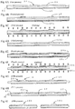
- a method for manufacturing the power module substrate 10b according to one embodiment shown in Figs. 4A and 4B described above will now be described with reference to Figs. 6A to 6I . More specifically, the method for manufacturing the power module substrate including the area 15 (the first copper circuit plate 12a) without the third portion 15c between the first portion 15a and the second portion 15b will now be described with reference to Figs. 6A to 6I .
- the method for manufacturing the power module substrates 10, 10a, 10b, or 10c according to one embodiment, each of which includes the island-shaped copper circuit plate 12 arranged on one main surface of the ceramic plate 11 and the heat dissipation copper plate 13 arranged on the other main surface, is typically classified into two methods: a method for manufacturing a power module substrate 10, 10a, 10b, or 10c as an individual piece; and a method for preparing a collective substrate for power modules including a large ceramic plate 11 on which a plurality of individual power module substrates 10, 10a, 10b, or 10c are arranged, and then cutting the collective substrate into individual pieces.
- the method for manufacturing the power module substrate according to the present embodiment mainly includes preparing a large ceramic plate (first process shown in Fig. 6A ), joining a large copper plate to each of the two main surfaces of the large ceramic plate (first process shown in Fig. 6A ), preparing a collective substrate for power modules by forming a pattern to be a copper circuit plate 12 and a heat dissipation copper plate 13 (second to fifth processes shown in Figs. 6B to 6I ), and optionally cutting the collective substrate for power modules into individual power module substrates 10, 10a, 10b, or 10c (not shown).
- a flat large ceramic plate 21 including a plurality of ceramic plates 11 for individual power module substrates 10b is prepared.
- the large ceramic plate 21 is prepared by cutting a ceramic green sheet into a quadrangle with an intended size, and firing the cut piece of the ceramic green sheet.
- An oxide ceramic green sheet is fired at a high temperature of 1500 °C or higher in an atmosphere.
- a nitride ceramic green sheet is fired at a high temperature of 1600 °C or higher in a nitrogen atmosphere.
- the DCB using heat is direct bonding achieved by arranging a large copper plate 22 on one main surface of the large ceramic plate 21 and a large copper plate 23 on the other main surface of the large ceramic plate 21, maintaining the facing surfaces between the plates in contact, and heating the structure at a temperature of 1065 to 1083 °C (the melting point of copper) to form an eutectic of Cu-Cu 2 O on the interface between the large ceramic plate 21 and the large copper plate 22, and also on the interface between the large ceramic plate 21 and the large copper plate 23, and then cooling the structure to join the large copper plates 22 and 23 directly onto the large ceramic plate 21 without a bond.
- the brazing using an active metal brazing material is liquid phase bonding achieved by arranging a brazing filler metal (e.g., a Ag-Cu alloy containing an activated metal, such as Ti or Zr, and having a lower melting point than copper) between one main surface of the large ceramic plate 21 and the large copper plate 22, and between the other main surface of the large ceramic plate 21 and the large copper plate, and then heating the structure at a temperature of about 800 °C to allow liquid-phase bonding of the large ceramic plate 21 and the large copper plates 22 and 23.
- a brazing filler metal e.g., a Ag-Cu alloy containing an activated metal, such as Ti or Zr, and having a lower melting point than copper
- the large copper plate 22 for the copper circuit plate 12 and the large copper plate 23 for the heat dissipation copper plate 13 may have any thicknesses
- the large copper plate 23 for the heat dissipation copper plate 13 may have the thickness approximate to the second portion 15b as described below.
- a first etching resist film 25 is formed in the area to be the first portion 15a, on which the semiconductor device 14 is to be mounted, on the large copper plate 22.
- a first etching resist film 25a is formed to cover the entire surface of the large copper plate 23, which is to be the heat dissipation copper plate 13.
- the first etching resist films 25 and 25a may be formed with any method.
- the first etching resist films 25 and 25a may be formed by the inkjet method or other methods described below.
- ink containing a photoresist solution is directly ejected and applied onto the large copper plates 22 and 23, and the applied ink is photocured to form the first etching resist films 25 and 25a.
- the first etching resist films 25 and 25a may be formed with methods other than the inkjet method including, for example, applying a photoresist paste onto the large copper plates 22 and 23 by screen printing, and photocuring the printed photoresist paste.
- Other methods include a dry film method implemented by attaching a photoresist dry film on the large copper plates 22 and 23, placing a pattern mask in contact with the dry film, photocuring the patterned portion exposed from the mask, then removing the pattern mask, and removing the dry film uncured portion to form the pattern at intended positions.
- the first etching resist films 25 and 25a may be formed at intended positions of the large copper plates 22 and 23 by directly applying a photoresist solution, in place of the dry film, onto the top surfaces of the large copper plates 22 and 23 using, for example, a roll coater, or immersing a joined structure 24 into the photoresist solution to form the first etching resist films 25 and 25a on the large copper plates 22 and 23, then drying the films and placing a pattern mask in contact with the dried films (the first etching resist films 25 and 25a), photocuring the patterned portion exposed from the pattern mask, then removing the pattern mask, and removing uncured portions of the dried films.
- the portion exposed from the first etching resist films 25 and 25a of the large copper plate 22 is etched to have a thickness smaller than the thickness of the first portion 15a, for example, to half (or substantially half) the thickness of the first portion 15a.
- the etching is performed by corroding and removing the large copper plate 22 using an acid etching solution (e.g., ferric chloride (FeCl 3 ) or copper chloride (CuCl 2 )) or an alkaline etching solution (e.g., a solution as a mixture of copper oxide (CuO) and ammonium chloride (NH 4 Cl)).
- an acid etching solution e.g., ferric chloride (FeCl 3 ) or copper chloride (CuCl 2 )
- an alkaline etching solution e.g., a solution as a mixture of copper oxide (CuO) and ammonium chloride (NH 4 Cl)
- the first etching resist films 25 and 25a are then removed by strip
- the second copper circuit plate 12b has the same thickness as the second portion 15b in the present embodiment, the second copper circuit plate 12b may not have the same thickness as the first portion 15a or as the second portion 15b. Further, the surface of the etched area of the copper plate may not be flat, but all the etched areas of the copper plate (the large copper plate 22) have at least a smaller thickness than the non-etched areas of the copper plate (the large copper plate 22).
- a second etching resist film 25b is formed in the area to be the copper circuit plate 12 on the large copper plate 22 by the inkjet method using ink containing a photoresist solution.
- a third etching resist film 25c is also formed in the area to be the heat dissipation copper plate 13 on the large copper plate 23 at the same time, the third etching resist film 25c may not be formed particularly by the inkjet method, and may be formed by other methods as described above.
- the large copper plates 22 and 23 exposed from the second and third etching resist films 25b and 25c are etched with the same method as described above to expose the surfaces of the intended portions of the large ceramic plate 21 to define the outer shapes of the copper circuit plate 12 and the heat dissipation copper plate 13 in the resultant individual power module substrates.
- the photoresist ink is directly ejected onto the surfaces of the copper plates (the large copper plates 22 and 23) to form a pattern.
- the pattern can be precisely formed on the surfaces of the copper plates that may not be flat, unlike other methods.
- the inkjet method is usable for objects with surfaces that are not flat.
- the inkjet method thus allows the second etching resist film 25b to adhere, with high positional accuracy, at intended positions of the large copper plate 22 with surface protrusions and recesses. This can prevent the etching solution from entering the interface between the large copper plate 22 and the etching resist film that adheres to the film, and allows the copper circuit plate 12 to form in an accurate shape.
- the first and third etching resist films 25, 25a, and 25c are formed on the flat large copper plates 22 and 23, and thus may not use the inkjet method.
- the second and third etching resist films 25b and 25c are removed from the top surfaces of a plurality of sets of copper circuit plates 12 and a plurality of sets of heat dissipation copper plates 13 to form a collective substrate 26 for power modules including a plurality of individual power module substrates 10b is arranged into a collective structure.
- laser scribe lines 27 are formed on the large ceramic plate 21.
- the laser scribe lines 27 are used to cut the collective substrate 26 for power modules into individual power module substrates 10b.
- the collective substrate 26 for power modules having the laser scribe lines 27 may be shipped as a completed product.
- the collective substrate 26 for power modules with such laser scribe lines 27 includes the first portions 15a that are regularly arranged on the large ceramic plate 21, and thus allows the semiconductor devices 14 to be efficiently mounted on the first portions 15a.
- the collective substrate 26 for power modules thus increases the productivity of the final products.
- the collective substrate 26 for power modules is then cut along the laser scribe lines 27 into individual pieces to easily yield individual power module substrates 10b.
- the laser scribe lines 27 can be easily formed using, for example, a typical yttrium aluminum garnet (YAG) laser or a CO 2 laser.
- the method for manufacturing the power module substrate 10b according to the present embodiment allows formation of the copper circuit plate 12 with precise surface protrusions and recesses. This structure allows heat generated from the semiconductor device 14 mounted on thick areas (first portion15a) in the copper circuit plate 12 to be promptly dissipated outside.
- the method for manufacturing the power module substrate according to the present embodiment further allows the copper circuit plate 12 in the power module substrate 10b to have relatively thinner portions (the second portion 15b, the third portion 15c, the second copper circuit plate 12b, and the heat dissipation copper plate 13) other than the portion on which the semiconductor device 14 is mounted.
- This structure can avoid separation of the edges of the copper circuit plate 12 and the heat dissipation copper plate 13 from the ceramic plate 11, and cracks in the ceramic plate 11 under heat stress at the joint interface between the ceramic plate 11 and the copper circuit plate 12, and at the joint interface between the ceramic plate 11 and the heat dissipation copper plate 13 resulting from the different thermal expansion coefficients of ceramics and copper.
- the method for manufacturing the power module substrate 10c (refer to Figs. 5A and 5B ), which includes the first copper circuit plate 12a having the third portion 15c arranged between the first portion 15a and the second portion 15b, will now be described with reference to Figs. 7A to 7D .
- the method for manufacturing the power module 10c according to the modification of the present invention includes the same first to fourth processes (from Figs. 6A to 6F ) as the processes included in the method for manufacturing the power module substrate 10b.
- the second etching resist film 25b is removed from the joined structure 24 that has undergone the fourth process shown in Fig. 6F .
- a fourth etching resist film 25d is formed by the inkjet method on each of the first and second copper circuit plates 12a and 12b, which are formed from the large copper plate 22.
- the fourth etching resist film 25d has an opening, or a groove surrounding the first portion 15a of the first copper circuit plate 12a, and covers the entire surface of the first copper circuit plate 12a except the opening.
- the fourth etching resist film 25d further covers the entire surface of the second copper circuit plate 12b.
- the fourth etching resist film 25d is formed on the side surfaces defining the first portion 15a of the first copper circuit plate 12a, the side surfaces defining the second portion 15b, and the side surfaces defining the second copper circuit plate 12b.
- the fourth etching resist film 25d is not formed only at positions where the third portions 15c are to be formed on the upper surface of the first copper circuit plate 12a, and the fourth etching resist film 25d is formed on all the remaining other surfaces of the first copper circuit plate 12a (the upper surface and the side surfaces).
- the surface of the first copper circuit plate 12a exposed from the opening of the fourth etching resist film 25d is etched to form the third portion 15c, which has a smaller thickness than the second portion 15b.
- the fourth etching resist film 25d and the third etching resist film 25c are then removed.
- the inkjet method with which a pattern is formed by directly ejecting photoresist ink onto the surface of the copper plate to be the copper circuit plate 12, is usable to form a pattern with high positional accuracy on the surface of the copper plate to be the copper circuit plate 12 that may not be flat, unlike the other methods described above.
- the fourth etching resist film 25d can adhere at intended positions of the surface of the copper plate to be the copper circuit plate 12, or more specifically, onto the upper surface of the first copper circuit plate 12a with protrusions and recesses, the side surfaces defining the first circuit substrate 12a, and the side surfaces defining the second circuit substrate 12b. This can prevent the etching solution from entering the interface between the fourth etching resist film 25d and the first circuit substrate 12a, to which the fourth etching resist film 25d adheres. This enables accurate formation of the first circuit substrate 12a with an intended shape.
- the method for manufacturing the power module substrate according to the modification of the present invention can form the power module substrate 10c including the first copper circuit plate 12a with precise protrusions and recesses, and the third portion 15c to receive solder that can overflow from the first portion 15a when the semiconductor device 14 is mounted onto the first portion 15a.
- the method for manufacturing the power module according to the modification of the present invention includes forming laser scribe lines 27 on the large ceramic plate 21 to be used to cut individual power module substrates 10b from the power module collective substrate 26a, in the same manner as the method described above for manufacturing the power module substrate 10b.
- cutting the collective substrate along the laser scribe lines 27 on the large ceramic substrate 21 easily yields the individual power module substrates 10c.
- the power module collective substrate 26a having the laser scribe lines 27 shown in Fig. 7C may be shipped as a completed product.
- the power module collective substrate 26a with such laser scribe lines 27 includes the first portions 15a that are regularly arranged on the large ceramic plate 21, and allows the semiconductor devices 14 to be efficiently mounted on the first portions 15a.
- the power module collective substrate 26a having the laser scribe lines 27 increases the productivity of the final products.
- the process for cutting the power module collective substrate 26a into individual pieces will be performed after the semiconductor devices 14 are mounted on the first portions 15a.
- the power module substrate and the power module collective substrate, and the method for manufacturing the power module substrate according to one embodiment are used for devices that can suddenly receive high voltage and can promptly dissipate heat generated from the devices to maintain high reliability.
- Examples of such devices include electronics devices for household use or business use, such as air conditioners, electronics devices for controlling, for example, robots and elevators, and electronics devices used in, for example, automobiles and trains.
Landscapes
- Engineering & Computer Science (AREA)
- Ceramic Engineering (AREA)
- Chemical & Material Sciences (AREA)
- Mechanical Engineering (AREA)
- Cooling Or The Like Of Semiconductors Or Solid State Devices (AREA)
Abstract

Description
- The present invention relates to a power module substrate, including a ceramic plate and a copper plate joined together for mainly mounting a power semiconductor device, and a collective substrate for power modules, and a method for manufacturing the power module substrate.
- A substrate for a power module includes a ceramic plate, an island-shaped copper circuit plate arranged on one main surface of the ceramic plate, and a heat dissipation copper plate arranged on the other main surface of the ceramic plate. This power module substrate is used for mounting a power semiconductor device, such as a power integrated circuit (IC) or an insulated gate bipolar transistor (IGBT), or for mounting a passive device, such as a capacitor. Recent power semiconductor devices consume more power, and generate more heat. Substrates for power modules may thus need to have higher heat resistance, heat dissipation, and insulation.
- A power module substrate includes a ceramic plate to increase heat resistance and insulation. A power module substrate may also include a joined structure of a copper plate and a ceramic plate to increase heat dissipation. A power module substrate is typically designed to dissipate heat generated from a semiconductor device mounted on its copper circuit plate downward through the copper circuit plate, a ceramic plate, and a heat dissipation copper plate. However, the power module substrate including the joined structure of the ceramic plate and the copper plate can have issues including lower heat dissipation through the ceramic plate with low heat conductivity, and separation of the edges of the copper plate from the ceramic plate or cracks in the ceramic plate under heat stress at the joint interface between the ceramic plate and the copper plates resulting from the different thermal expansion coefficients of ceramics and copper.
- To increase heat dissipation, a power module substrate may include, for example, a ceramic plate formed from a highly conductive ceramic, such as aluminum nitride. However, the ceramic plate formed from aluminum nitride is very expensive. To increase heat dissipation, the power module substrate may include a thinner ceramic plate. However, the thinner ceramic plate formed from an alumina-based ceramic can have a lower strength. A silicon nitride-based ceramic, which has high strength, may be used. However, the ceramic plate formed from silicon nitride is very expensive. To increase heat dissipation, the power module substrate may include a thicker copper plate joined with a ceramic plate. However, the increased heat stress at the joint interface between the ceramic plate and the copper plates resulting from the different thermal expansion coefficients of ceramics and copper may cause separation of the edges of the copper plate and cracks in the ceramic plate. A thin ceramic plate with high heat dissipation made of zirconia added alumina having higher strength than ceramics made of alumina is available recently. This ceramic plate joined with a relatively thick copper plate intends to reduce separation of the edges of the copper plate and to minimize cracks in the ceramic plate under heat stress at the joint interface between the ceramic plate and the copper plate resulting from the different thermal expansion coefficients of ceramics and copper.
- The joined structure of the ceramic plate and the copper plates is typically prepared by brazing the copper plates on the two main surfaces of the ceramic plate using an active metal brazing material, or by direct copper bonding (DCB) using heat, which directly bonds the ceramic plate and the copper plates with heat. Brazing using the active metal brazing material allows an active metal brazing material layer, such as a Ag/Cu/Ti layer, to form between the ceramic plate and the copper plates. The brazing layer is expected to serve as a buffer layer against heat stress. However, the active metal brazing material layer can slightly degrade heat dissipation. The DCB using heat is suited for bonding an oxide ceramic plate of, for example, alumina with copper plates. With the DCB using heat, the oxide ceramic plate and the copper plates have their surfaces placed in contact with each other, and are heated to form an eutectic of Cu-Cu2O on their interfaces, and the plates are then cooled for joining. The power module substrate prepared by the DCB using heat includes the copper plates and the ceramic plate joined either directly, or with a very thin copper oxide layer between them, and thus has high heat transfer, or high heat dissipation, at the interfaces between the ceramic plate and the copper plates. However, the ceramic plate or the copper plates still need some measures to reduce stress at the joint interfaces between the ceramic plate and the copper plate edges.
- The joined structure of the ceramic plate and the copper plates can have its copper plate surface masked using an etching resist having an intended pattern. The uncovered portions of the copper plate may then be removed by chemical corrosion (etching) to yield the copper circuit plate with an intended shape. The power module substrate is typically obtained from a collective substrate including a plurality of areas to be a plurality of power module substrates, which are then cut along the splitting grooves formed along the boundaries of the power module substrates.
- A power module substrate known in the art may have its copper plate with protrusions and recesses on the surface to reduce stress at the joint interface between a ceramic plate and the edges of the copper plate, to position a semiconductor device for soldering, or to prevent overflow of solder (refer to, for example,
Patent Literatures - A method for manufacturing a power module substrate known in the art may form a metal circuit pattern through the three processes: (1) half-etching a metal plate into the shape of a circuit pattern, (2) joining the etched surface with a ceramic plate, and (3) applying an etching resist on the surface of the metal plate that is not joined with the ceramic plate, and half-etching the plate to form a step (refer to, for example, Patent Literature 4). The etching resist film is formed by applying a known ultraviolet curable or thermosetting resist paste onto the metal plate by screen printing, and then curing the paste.
-
- Patent Literature 1: Japanese Unexamined Patent Application Publication No.
4-103150 - Patent Literature 2: Japanese Unexamined Patent Application Publication No.
10-242330 - Patent Literature 3: Japanese Unexamined Patent Application Publication No.
10-242331 - Patent Literature 4: Japanese Unexamined Patent Application Publication No.
2007-134563 - However, the power module substrate and the method for manufacturing the power module substrate can have issues described below.
- To promptly dissipate heat generated from an electronic component, particularly from a semiconductor device that reaches high temperature, the thickness of the copper plate as a mount for the semiconductor device may be increased to increase the range of heat transfer and diffusion toward the ceramic plate. However, increasing the thickness of the semiconductor device mounting area of the copper plate increases the thickness of the entire island-shaped copper circuit plate. This increases heat stress at the joint interface of the ceramic plate and the copper plate resulting from the different thermal expansion coefficients of ceramics and copper. Although the copper plate with a smaller thickness can reduce heat stress at the joint interface of the ceramic plate and the copper plate, the thinner copper plate disables prompt heat dissipation from the semiconductor device.
- The power module substrates described in Japanese Unexamined Patent Application Publication Nos.
4-103150 10-242330 10-242331 - For the power module substrate described for example in Japanese Unexamined Patent Application Publication No.
2007-134563 - In response to this issue, one aspect of the present invention provides a substrate for a power module that allows prompt heat dissipation from a semiconductor device, and avoid separation of the edges of a copper plate from a ceramic plate and cracks in the ceramic plate under heat stress at the joint interface of the ceramic plate and the copper plate resulting from the different thermal expansion coefficients of ceramics and copper.
- Another aspect of the present invention provides a method for manufacturing a substrate for a power module including a copper circuit plate with precise protrusions and recesses capable of promptly dissipating heat generated from a semiconductor device and reducing heat stress at the joint interface between a ceramic plate and the copper plate resulting from the different thermal expansion coefficients of ceramics and copper.
- Another aspect of the present invention provides a method for manufacturing a substrate for a power module for forming a copper circuit plate with precise protrusions and recesses including a portion for preventing overflow of solder when a semiconductor device is joined with solder.
- A first aspect of the present invention provides a substrate for a power module including a ceramic plate, a copper circuit plate on a main surface of the ceramic plate, and a heat dissipation copper plate on a surface of the ceramic plate opposite to the main surface. The copper circuit plate includes at least one first copper circuit plate, and at least one second copper circuit plate different from the first copper circuit plate. The first copper circuit plate includes a first portion on which a semiconductor device is mountable, and a second portion having a smaller thickness than the first portion. The second portion is outward from and surrounding the first portion.
- A second aspect of the present invention may provide the substrate for a power module according to the first aspect, in which the first copper circuit plate further includes a third portion between the first portion and the second portion, and the third portion has a smaller thickness than the second portion.
- A third aspect of the present invention may provide the substrate for a power module according to the first aspect or the second aspect, in which the second copper circuit plate has a smaller thickness than the first portion.
- A fourth aspect of the present invention may provide a collective substrate for power modules, in which the collective substrate includes a plurality of the substrates for a power module according to any one of the first to third aspects that are arranged in a matrix and are integral with one another.
- A fifth aspect of the present invention provides a method for manufacturing a substrate for a power module. The method includes joining a first large copper plate, and a second large copper plate on two surfaces of a ceramic plate by direct copper bonding using heat or brazing using an active metal brazing material, forming a first etching resist film on each of the first and second large copper plates, etching a portion of each of the first and second large copper plates without the first etching resist film to reduce a thickness of the portion, removing the first etching resist film, forming a second etching resist film on the first large copper plate and a third etching resist film on the second large copper plate, etching a portion of each of the first and second large copper plates without the second etching resist film and the third etching resist film to expose the ceramic plate, removing the second etching resist film, removing the third etching resist film, and forming laser scribe lines for cutting on a surface of the ceramic plate. The second etching resist film is formed with an inkjet method.
- The method according to the fifth aspect for manufacturing a substrate for a power module may further include, between the removing the second etching resist film and the removing the third etching resist film, forming a fourth etching resist film with an inkjet method on the first large copper plate from which the second etching resist film has been removed, and etching a portion of the first large copper plate without the fourth etching resist film to reduce a thickness of the portion to be smaller than a thickness of the etched portion of each of the first and second large copper plates without the first etching resist film.
- The power module substrate according to the first aspect of the present invention includes the copper circuit plate including the first copper circuit plate and the second copper circuit plate different from the first copper circuit plate. The first copper circuit plate includes the first portion on which a semiconductor device is mountable, and the second portion having a smaller thickness than the first portion. The second portion is outward from and surrounds the first portion. The thickness of the first portion of the copper circuit plate, on which a semiconductor device is mountable, can thus be increased. This structure can increase the range of heat transfer and diffusion from the first portion, and allows heat generated from the semiconductor device to be promptly transferred to the heat dissipation copper plate arranged under the ceramic plate.
- Also, the second portion of the copper circuit plate has a smaller thickness than the first portion of the copper circuit plate, and thus can reduce heat stress at the joint interface between the ceramic plate and the copper plate resulting from the different thermal expansion coefficients of ceramics and copper. This structure avoids separation of the edges of the copper circuit plate from the ceramic plate, and cracks in the ceramic plate.
- The power module substrate according to the second aspect of the present invention includes the third portion surrounding the first portion. The third portion has a smaller thickness than the second portion. Thus, when a semiconductor device is joined to the first portion with a bond (e.g., solder), the bond that can overflow from the first portion is blocked by the step formed between the second portion and the third portion. This prevents a short circuit between the first copper circuit plate and the second copper circuit plate.
- The power module substrate according to the third aspect of the present invention includes the second copper circuit plate having a smaller thickness than the first portion of the copper circuit plate, and thus can reduce heat stress at the joint interface between the ceramic plate and the second copper circuit plate resulting from the different thermal expansion coefficients of ceramics and copper. This structure avoids separation of the edges of the second copper circuit plate from the ceramic plate, and cracks in the ceramic plate.
- For the first copper circuit plate having the third portion, the bond that can overflow from the first portion when a semiconductor device is joined to the first portion with a bond is blocked by the step formed between the second portion and the third portion. This prevents a short circuit between the first copper circuit plate and the second copper circuit plate.
- The collective substrate for power modules according to the fourth aspect of the present invention includes first portions that are arranged regularly for mounting semiconductor devices. This allows semiconductor devices to be efficiently mounted onto the first portions.
- The collective substrate for power modules according to the fourth aspect of the present invention increases the productivity of the final products.
- The method for manufacturing a substrate for a power module according to the fifth aspect of the present invention is a method for manufacturing the power module substrate according to the first aspect of the present invention and the power module substrate according to the fourth aspect of the present invention. The method according to the fifth aspect enables manufacture of the power module substrate that promptly dissipates heat generated from the semiconductor device, and reduces heat stress at the joint interface between the ceramic plate and the copper plate resulting from the different thermal expansion coefficients of ceramics and copper to avoid separation of the edges of the copper circuit plate from the ceramic plate and cracks in the ceramic plate in the resultant power module substrate.
- The method for manufacturing a substrate for a power module according to the fifth aspect of the present invention uses an inkjet method to form the second etching resist film. The resultant second etching resist film can have a cross-section in correspondence with any protrusions and recesses formed on the large copper plate surface. In other words, the second etching resist film can be formed at intended positions with high accuracy on the large copper plate with surface protrusions and recesses. This method easily forms the second etching resist film without rupture or breaks on any surface protrusions and recesses of the large copper plate. The subsequent etching thus forms precise protrusions and recesses on the large copper plate.
- The method for manufacturing a substrate for a power module according to the sixth aspect of the present invention uses an inkjet method to form the fourth etching resist film. The resultant fourth etching resist film can have a cross-section in correspondence with any protrusions and recesses formed on the large copper plate surface. In other words, the fourth etching resist film can be formed at intended positions with high accuracy on the large copper plate with surface protrusions and recesses. The method forms the fourth etching resist film without rupture or breaks on any surface protrusions and recesses of the large copper plate. The subsequent etching thus forms precise protrusions and recesses on the large copper plate.
-
-
Fig. 1A is a plan view of a power module substrate according to one embodiment of the present invention, andFig. 1B is an enlarged longitudinal cross-sectional view taken along line A-A' inFig. 1A ; -
Figs. 2A and 2B are diagrams describing heat dissipation for power module substrates that differ from each other in the thickness of copper plates; -
Fig. 3A is a plan view of a power module substrate according to a modification, andFig. 3B is an enlarged longitudinal cross-sectional view taken along line B-B' inFig. 3A ; -
Fig. 4A is a plan view of the power module substrate according to another modification, andFig. 4B is a longitudinal cross-sectional view taken along line C-C' inFig. 4A ; -
Fig; 5A is a plan view of the power module substrate according to yet another modification, andFig. 5B is a longitudinal cross-sectional view taken along line D-D' inFig. 5A ; -
Figs. 6A to 6I are diagrams describing a method for manufacturing the power module substrate; and -
Figs. 7A to 7D are diagrams describing a method for manufacturing the power module substrate according to a modification. - A substrate for a power module according to one embodiment of the present invention will now be described with reference to
Figs. 1A and 1B . - As shown in
Figs. 1A and 1B , asubstrate 10 for a power module according to the present embodiment includes a ceramic plate 11, and an island-shapedcopper circuit plate 12, which is joined to one main surface of the ceramic plate 11. Theentire circuit substrate 12 forms an electric circuit. Thepower module substrate 10 further includes a heat dissipation copper plate 13, which is joined to the other main surface of the ceramic plate 11 to cover the entire surface of the other main surface (where the term entire includes substantially entire). The heat dissipation copper plate 13 dissipates heat generated from an electronic component (e.g., a semiconductor device 14) mounted on thecopper circuit plate 12 downward (toward the other main surface). - The
copper circuit plate 12 includes a firstcopper circuit plate 12a for mounting the electronic component, such as thesemiconductor device 14, and secondcopper circuit plates 12b different from the firstcopper circuit plate 12a. - Although the single first
copper circuit plate 12a is arranged on one main surface of the ceramic plate 11 in the present embodiment, two or more firstcopper circuit plates 12a may be arranged on one main surface of the ceramic plate 11. - Although the multiple second
copper circuit plates 12b are arranged on one main surface of the ceramic plate 11 in the present embodiment, a single secondcopper circuit plate 12b may be arranged on the surface. - Although the
semiconductor device 14 is mounted on the firstcopper circuit plate 12a as one example of an electronic component inFigs. 1 to 5 for easy understanding of the advantageous effects of the power module substrate according to the present embodiment, the electronic component, such as thesemiconductor device 14, may not be an element to be included in the claimed invention. - In use, the
power module substrate 10 according to the present embodiment has an electronic component, such as thesemiconductor device 14, joined to each of the firstcopper circuit plates 12a with a bond, such as solder. Typically, a connecting terminal mounted on the upper surface of thesemiconductor device 14 is electrically connected to the secondcopper circuit plate 12b with a bonding wire (not shown), and the secondcopper circuit plate 12b is electrically connected to an external circuit with a metal lead. Thepower module substrate 10 according to the present embodiment promptly transfers heat generated from thepower semiconductor device 14, such as a power integrated circuit (IC) or an insulated gate bipolar transistor (IGBT), downward through thecopper circuit plate 12 to the heat dissipation copper plate 13 (on the other main surface of the ceramic plate 11), and further to a fin heatsink or water cooling heatsink (not shown), which is attached to the heat dissipation copper plate 13. The performance of the device is thus retained. - The thickness of the copper plates (the
copper circuit plate 12 and the heat dissipation copper plate 13) largely affects any improvement in the heat dissipation of thepower module substrate 10. The heat dissipation that can differ depending on the thickness of the copper plates (the firstcopper circuit plate 12a) will now be described with reference toFigs. 2A and 2B . Heat generated from thesemiconductor device 14 mounted on the copper circuit plate 12 (firstcopper circuit plate 12a) is promptly transferred from the upper surface toward the lower surface of thecopper circuit plate 12, which has high heat conductivity, while spreading downward at a substantially constant angle α. The heat reaching the lower surface of thecopper circuit plate 12 is then transferred substantially at right angles from the upper surface toward the lower surface of the ceramic plate 11. Further, the heat reaching the lower surface of the ceramic plate 11 is promptly transferred from the upper surface toward the lower surface of the heat dissipation copper plate 13, which has high heat conductivity, while diverging downward at a substantially constant angle α. The heat reaching the lower surface of the heat dissipation copper plate 13 is then directed outside by air cooling using, for example, heat radiating fins or a heatsink plate (not shown), or by water cooling (not shown) using circulating water along the surface of the heat dissipation copper plate 13. As shown inFig. 2A , X is the transfer range of heat reaching the lower surface of the heat dissipation copper plate 13 in the structure including a thickcopper circuit plate 12 and a thick heat dissipation copper plate 13. As shown inFig. 2B , Y is the transfer range of heat reaching the lower surface of the heat dissipation copper plate 13 in the structure including a thincopper circuit plate 12 and a thin heat dissipation copper plate 13. In this case, X > Y The heat dissipation is thus higher as the copper plates (thecopper circuit plate 12 and the heat dissipation copper plate 13) are thicker, and is lower as the copper plates (thecopper circuit plate 12 and the heat dissipation copper plate 13) are thinner. - In manufacturing the
power module substrate 10, the temperature at which thecopper circuit plate 12 or the heat dissipation copper plate 13 is joined to the ceramic plate 11 typically reaches 800 °C or higher, or can reach 1000 °C or higher. This temperature is far higher than the temperature at which resin and copper for a plastic circuit substrate are joined together in the process of manufacturing the plastic circuit substrate. The use of a thickercopper circuit plate 12 and a thicker heat dissipation copper plate 13 joined to the ceramic plate 11 to increase heat dissipation in thepower module substrate 10 undergoing such manufacturing processes can cause separation of the edges of thecopper circuit plate 12 and the heat dissipation copper plate 13 from the ceramic plate 11 or can cause cracks in the ceramic plate 11 under heat stress resulting from the different thermal expansion coefficients of ceramics and copper at the joint interfaces of the ceramic plate 11 and the copper plates (thecopper circuit plate 12 and the heat dissipation copper plate 13). When thecopper circuit plate 12 and the heat dissipation copper plate 13 are joined to the ceramic plate 11, thecopper circuit plate 12 and the heat dissipation copper plate 13 can undergo distortion caused by the different thermal expansion coefficients of ceramics and copper. When such distortion occurs unevenly across thecopper circuit plate 12 and the heat dissipation copper plate 13, the power module substrate can warp. To reduce such warpage of the power module substrate, the thicknesses of thecopper circuit plate 12 and the heat dissipation copper plate 13 are to be adjusted to allow thecopper circuit plate 12 and the heat dissipation copper plate 13 to have substantially the same volume. - The
power module substrate 10 according to the present embodiment includes the firstcopper circuit plate 12a, on which thesemiconductor device 14 is to be mounted. The firstcopper circuit plate 12a has anarea 15 including portions with varying thicknesses depending on their use in thecopper circuit plate 12. - The
area 15 includes a first portion 15a with the largest thickness, and a second portion 15b with a smaller thickness than the first portion 15a. The second portion 15b is outward from the first portion 15a, and surrounds the first portion 15a. In use, thepower module substrate 10 according to the present embodiment has an electronic component (e.g., the semiconductor device 14) joined to the thickest first portion 15a with a bond (e.g., solder). - The
power module substrate 10 according to the present embodiment allows thesemiconductor device 14 to be mounted on the thickest first portion 15a in the firstcopper circuit plate 12a, and thus can promptly transmit heat generated from thesemiconductor device 14 toward the lower surface (toward the other main surface), while increasing the range of heat transfer and diffusion downward at a substantially constant angle α. Further, heat generated from thesemiconductor device 14 can be promptly transferred though the heat dissipation copper plate 13 arranged under the ceramic plate 11 toward the lower surface, while increasing the range of heat transfer and diffusion downward at a substantially constant angle α. This allows heat generated from thesemiconductor device 14 to be efficiently dissipated outside through a heatsink (not shown) joined to the heat dissipation copper plate 13. In thepower module substrate 10 according to the present embodiment, the second portion 15b of the firstcopper circuit plate 12a has a smaller thickness than the first portion 15a of the firstcopper circuit plate 12a, and thus can reduce heat stress resulting from the different thermal expansion coefficients of ceramics and copper at the joint interface between the ceramic plate 11 and the secondcopper circuit plate 12b. This structure avoids separation of the edges of thecopper plate 12 from the ceramic plate 11, and cracks in the ceramic plate 11. - To reduce warpage of the power module substrate, the heat dissipation copper plate 13 arranged on the lower surface of the ceramic plate 11 may have a thickness falling between the thickness of the first portion 15a and the thickness of the second portion 15b. Although not particularly limited, the thickness of the second
copper circuit plate 12b greater than the thickness of the first portion 15a increases heat stress at the joint interface between the ceramic plate 11 and the secondcopper circuit plate 12b resulting from the different thermal expansion coefficients of ceramics and copper. The resultant structure may not easily avoid separation of the edges of the secondcopper circuit plate 12b from the ceramic plate 11 or fracture caused by cracks in the ceramic plate 11. - Although not limiting, the ceramic plate 11 for the
power module substrate 10 according to the present embodiment may be formed from an oxide of mainly alumina, such as alumina or alumina-zirconia, or may be formed from silicon nitride or aluminum nitride. These ceramics may not have a purity of 100%, and may contain 5% or less by weight of other components that aids sintering of ceramics, such as silicon, magnesium, or a rare earth element. Although the ceramic plate 11 for thepower module substrate 10 typically has a thickness in the range of 0.2 to 1.0 mm, the ceramic plate 11 is to be thinner to increase heat dissipation unless the strength and the insulation of the ceramic plate 11 are degraded. To join thecopper circuit plate 12 and the heat dissipation copper plate 13 to the ceramic plate 11 with direct copper bonding (DCB) using heat, an alumina-based oxide ceramic including, for example, alumina or alumina-zirconia, may be used as the ceramic plate 11. As the ceramic plate 11, a nitride ceramic, such as silicon nitride or aluminum nitride containing 5% or less by weight of other components such as silicon, magnesium, or a rare earth element, may also be used. When a nitride ceramic including, for example, silicon nitride or aluminum nitride, is used for the ceramic plate 11 for thepower module substrate 10, thecopper circuit plate 12 and the heat dissipation copper plate 13 can be joined to the ceramic plate 11 by brazing using an active metal brazing material. - The material for the
copper circuit plate 12 and the heat dissipation copper plate 13 for thepower module substrate 10 according to the present embodiment may be oxygen-free copper, tough pitch copper, or phosphorus deoxidized copper, which has high electrical conductivity and thermal conductivity, and is inexpensive. Thecopper circuit plate 12 and the heat dissipation copper plate 13 may contain impurities unless such impurities affect the characteristics of the material microstructure. The permissive amount of impurities, for example, silver or tin, is up to 0.05% by weight. Although the thickness of thecopper circuit plate 12 and the heat dissipation copper plate 13 for thepower module substrate 10 is typically in the range of 0.2 to 0.6 mm, the thickness may be 1.0 mm or more for use that needs heat dissipation. - When the
semiconductor device 14 is joined to the first portion 15a with solder, the molten solder (bond) can overflow from the first portion 15a to the second portion 15b, and further from the second portion 15b to the ceramic plate 11. The flowing solder (bond) may reach an adjacent secondcopper circuit plate 12b, and cause a short circuit between thecopper circuit plate 12a and thecopper circuit plate 12b. In response to this, for example, Patent Literature 3 (Japanese Unexamined Patent Application Publication No.10-242331 Figs. 2 and3 of the literature, a technique for forming a ridge surrounding the semiconductor device on the surface of the copper circuit plate to prevent overflow of the solder. The ridge prevents overflow of solder for joining the semiconductor device to the copper circuit plate. However, this technique includes no consideration for heat dissipation from the semiconductor device. In the structure described inPatent Literature 3, the circuit plate (2) on the lower surface of the semiconductor device has a uniform thickness. Increasing the thickness of the circuit plate (2) to improve heat dissipation would cause the edges of the circuit plate (2) to easily separate from the ceramic substrate (1). In contrast, decreasing the thickness of the circuit plate (2) to prevent separation of the edges of the circuit plate (2) from the ceramic substrate (1) can lower the dissipation of heat generated from the semiconductor device. - In response to the above issue, a substrate for a power module according to a modification of the present invention shown in
Figs. 3A and 3B has been developed. - The power module substrate according to the modification of the present invention that can prevent overflow of solder will now be described with reference to
Figs. 3A and 3B . - As shown in
Figs. 3A and 3B , a power module 10a according to the modification of the present invention includes an island-shapedcopper circuit plate 12, which includes a firstcopper circuit plate 12a and a secondcopper circuit plate 12b on one main surface of the ceramic plate 11, and a heat dissipation copper plate 13 on the other main surface of the ceramic plate 11. In the power module substrate according to the modification of the present invention, the firstcopper circuit plate 12a, on which asemiconductor device 14 is to be mounted, has anarea 15 including portions with varying thicknesses depending on their use. More specifically, as shown inFigs. 3A and 3B , thearea 15 includes a third portion 15c between a first portion 15a and a second portion 15b included in thecopper circuit plate 12. The third portion 15c has a smaller thickness than the second portion 15b. In the power module substrate 10a according to the modification of the present invention, thecopper circuit plate 12 is thinner in the order of the first portion 15a, the second portion 15b, and the third portion 15c of thearea 15. In the same manner as for thepower module substrate 10 shown inFigs. 1A and 1B , the power module substrate 10a shown inFigs. 3A and 3B may include the secondcopper circuit plate 12b with any thickness. However, the secondcopper circuit plate 12b thicker than the first portion 15a increases heat stress at the joint interface between the ceramic plate 11 and the secondcopper circuit plate 12b resulting from the different thermal expansion coefficients of ceramics and copper. This structure may not easily avoid separation of the edges of the secondcopper circuit plate 12b from the ceramic plate 11 and cracks in the ceramic plate 11. Thus, the thickness of the secondcopper circuit plate 12b is to be smaller than the thickness of the first portion 15a in the power module substrate 10a according to the modification of the present invention as well. - The power module substrate 10a according to the modification of the present invention can promptly dissipate heat generated from the
semiconductor device 14, and can avoid separation of the edges of thecopper circuit plate 12 and the heat dissipation copper plate 13 from the ceramic plate 11 and cracks in the ceramic plate 11. The power module substrate 10a according to the modification of the present invention also allows the third portion 15c to receive any solder (bond) flowing out of the first portion 15a, and prevents the solder from flowing out of the second portion 15b when an electronic component, such as asemiconductor device 14, is joined to the first portion 15a with solder (bond). This prevents a short circuit between the firstcopper circuit plate 12a and an adjacent secondcopper circuit plate 12b. - As shown in
Figs. 4A and 4B , thepower module substrate 10 according to one embodiment may be modified as a substrate 10b for a power module having the secondcopper circuit plate 12b with a smaller thickness than the first portion 15a, or with the same thickness (or substantially the same thickness) as the thickness of the second portion 15b. - As shown in
Figs. 5A and 5B , the power module 10a according to the modification of the present invention may be a substrate 10c for a power module having the secondcopper circuit plate 12b with a smaller thickness than the first portion 15a, or with the same thickness (or substantially with the same thickness) as the thickness of the second portion 15b. - In particular, the power module substrates 10b and 10c shown in
Figs. 4A to 5B each including the secondcopper circuit plate 12b having the same thickness (or substantially with the same thickness) as the second portion 15b can be manufactured with simpler processes (refer to the method for manufacturing the power module substrate according to one embodiment described below), and thus improve productivity. - Further, the power module substrates 10b and 10c shown in
Figs. 4A to 5B each include the heat dissipation copper plate 13 arranged on the lower surface of the ceramic plate 11. The thickness of the heat dissipation copper plate 13 is determined to optimize the warpage of the power module substrates 10b and 10c. More specifically, the heat dissipation copper plate 13 has a thickness falling between the thickness of the first portion 15a and the thickness of the second portion 15b of the firstcopper circuit plate 12a, or a thickness falling between the thickness of the first portion 15a and the thickness of the secondcopper circuit plate 12b. - The power module substrates 10b and 10c shown in
Figs. 4A to 5B can thus promptly transmit heat generated from thesemiconductor device 14, which is mounted on the thickest first portion 15a in the firstcopper circuit plate 12a, toward the lower surface of the firstcopper circuit plate 12a, while increasing the range of heat transfer and diffusion downward at a substantially constant angle α. This structure further transfers heat generated from thesemiconductor device 14 toward the lower surface through the heat dissipation copper plate 13 arranged on the lower surface of the ceramic plate 11, while increasing the range of heat transfer and diffusion downward at the substantially constant angle α. In this manner, the power module substrates 10b and 10c shown inFigs. 4A to 5B , which have a long distance locally from thesemiconductor device 14 to the ceramic plate 11, can efficiently dissipate heat generated from thesemiconductor device 14 outside through a heatsink (not shown). - Additionally, the power module substrates 10b and 10c shown in
Figs. 4A to 5B have the second portion 15b and the secondcopper circuit plate 12b both having smaller thicknesses than the first portion 15a. This structure reduces heat stress at the joint interface between the ceramic plate 11 and the secondcopper circuit plate 12b, and at the joint interface between the ceramic plate 11 and the heat dissipation copper plate 13 resulting from the different thermal expansion coefficients of ceramics and copper, and can avoid separation of the edges of eachcopper circuit plate 12 and the edges of the heat dissipation copper plate 13 from the ceramic plate 11, and cracks in the ceramic plate 11. - In the
power module substrates 10 and 10a to 10c according to one embodiment shown inFigs. 1A and 1B , andFigs. 3A to 5B , if the second portion 15b, the third portion 15c, and the secondcopper circuit plate 12b have a smaller thickness than the first portion 15a or the second portion 15b, the second portion 15b, the third portion 15c, and the secondcopper circuit plate 12b each may not have a uniform thickness. - Although each of the
power module substrates 10 and 10a to 10c according to one embodiment is provided as an individual piece as shown inFigs. 1A ,3A ,4A and5A , a plurality of such substrates may be integrated into a collective substrate in which a plurality ofpower module substrates 10, 10a, 10b, or 10c are arranged in a matrix. - The collective substrate for power modules includes the first portions 15a in each of which the
semiconductor device 14 is to be mounted. The first portions 15a are arranged regularly on the ceramic plate 11. Thesemiconductor devices 14 can thus be efficiently mounted on the respective first portions 15a. - The collective substrate for power modules thus increases the productivity of the final products, which may be electronics devices for household use or business use, such as air conditioners, electronics devices for controlling, for example, robots and elevators, and electronics devices used in, for example, automobiles and trains.
- A method for manufacturing the power module substrate 10b according to one embodiment shown in
Figs. 4A and 4B described above will now be described with reference toFigs. 6A to 6I . More specifically, the method for manufacturing the power module substrate including the area 15 (the firstcopper circuit plate 12a) without the third portion 15c between the first portion 15a and the second portion 15b will now be described with reference toFigs. 6A to 6I . - The method for manufacturing the
power module substrates 10, 10a, 10b, or 10c according to one embodiment, each of which includes the island-shapedcopper circuit plate 12 arranged on one main surface of the ceramic plate 11 and the heat dissipation copper plate 13 arranged on the other main surface, is typically classified into two methods: a method for manufacturing apower module substrate 10, 10a, 10b, or 10c as an individual piece; and a method for preparing a collective substrate for power modules including a large ceramic plate 11 on which a plurality of individualpower module substrates 10, 10a, 10b, or 10c are arranged, and then cutting the collective substrate into individual pieces. - The manufacturing method using the large ceramic plate (the latter method) will now be described.
- The method for manufacturing the power module substrate according to the present embodiment mainly includes preparing a large ceramic plate (first process shown in
Fig. 6A ), joining a large copper plate to each of the two main surfaces of the large ceramic plate (first process shown inFig. 6A ), preparing a collective substrate for power modules by forming a pattern to be acopper circuit plate 12 and a heat dissipation copper plate 13 (second to fifth processes shown inFigs. 6B to 6I ), and optionally cutting the collective substrate for power modules into individualpower module substrates 10, 10a, 10b, or 10c (not shown). - In the first process, as shown in
Fig. 6A , a flat largeceramic plate 21 including a plurality of ceramic plates 11 for individual power module substrates 10b is prepared. The largeceramic plate 21 is prepared by cutting a ceramic green sheet into a quadrangle with an intended size, and firing the cut piece of the ceramic green sheet. An oxide ceramic green sheet is fired at a high temperature of 1500 °C or higher in an atmosphere. A nitride ceramic green sheet is fired at a high temperature of 1600 °C or higher in a nitrogen atmosphere. - A flat large copper plate 22, which is to be a
copper circuit plate 12, is joined to one main surface of the fired largeceramic plate 21, and a flatlarge copper plate 23, which is to be a heat dissipation copper plate 13, is joined to the other main surface of the largeceramic plate 21, both by the DCB using heat (when the largeceramic plate 21 is formed from an oxide ceramic) or by brazing using an active metal brazing material (when the largeceramic plate 21 is formed from a material other than an oxide ceramic). - The DCB using heat is direct bonding achieved by arranging a large copper plate 22 on one main surface of the large
ceramic plate 21 and alarge copper plate 23 on the other main surface of the largeceramic plate 21, maintaining the facing surfaces between the plates in contact, and heating the structure at a temperature of 1065 to 1083 °C (the melting point of copper) to form an eutectic of Cu-Cu2O on the interface between the largeceramic plate 21 and the large copper plate 22, and also on the interface between the largeceramic plate 21 and thelarge copper plate 23, and then cooling the structure to join thelarge copper plates 22 and 23 directly onto the largeceramic plate 21 without a bond. - The brazing using an active metal brazing material is liquid phase bonding achieved by arranging a brazing filler metal (e.g., a Ag-Cu alloy containing an activated metal, such as Ti or Zr, and having a lower melting point than copper) between one main surface of the large
ceramic plate 21 and the large copper plate 22, and between the other main surface of the largeceramic plate 21 and the large copper plate, and then heating the structure at a temperature of about 800 °C to allow liquid-phase bonding of the largeceramic plate 21 and thelarge copper plates 22 and 23. - Although the large copper plate 22 for the
copper circuit plate 12 and thelarge copper plate 23 for the heat dissipation copper plate 13 may have any thicknesses, thelarge copper plate 23 for the heat dissipation copper plate 13 may have the thickness approximate to the second portion 15b as described below. - In the subsequent second process, as shown in
Fig. 6B , a first etching resistfilm 25 is formed in the area to be the first portion 15a, on which thesemiconductor device 14 is to be mounted, on the large copper plate 22. A first etching resist film 25a is formed to cover the entire surface of thelarge copper plate 23, which is to be the heat dissipation copper plate 13. The first etching resistfilms 25 and 25a may be formed with any method. For example, the first etching resistfilms 25 and 25a may be formed by the inkjet method or other methods described below. - With the inkjet method, ink containing a photoresist solution is directly ejected and applied onto the
large copper plates 22 and 23, and the applied ink is photocured to form the first etching resistfilms 25 and 25a. - The first etching resist
films 25 and 25a may be formed with methods other than the inkjet method including, for example, applying a photoresist paste onto thelarge copper plates 22 and 23 by screen printing, and photocuring the printed photoresist paste. Other methods include a dry film method implemented by attaching a photoresist dry film on thelarge copper plates 22 and 23, placing a pattern mask in contact with the dry film, photocuring the patterned portion exposed from the mask, then removing the pattern mask, and removing the dry film uncured portion to form the pattern at intended positions. Further, the first etching resistfilms 25 and 25a may be formed at intended positions of thelarge copper plates 22 and 23 by directly applying a photoresist solution, in place of the dry film, onto the top surfaces of thelarge copper plates 22 and 23 using, for example, a roll coater, or immersing a joinedstructure 24 into the photoresist solution to form the first etching resistfilms 25 and 25a on thelarge copper plates 22 and 23, then drying the films and placing a pattern mask in contact with the dried films (the first etching resistfilms 25 and 25a), photocuring the patterned portion exposed from the pattern mask, then removing the pattern mask, and removing uncured portions of the dried films. - In the third process, as shown in
Fig. 6C , the portion exposed from the first etching resistfilms 25 and 25a of the large copper plate 22 is etched to have a thickness smaller than the thickness of the first portion 15a, for example, to half (or substantially half) the thickness of the first portion 15a. The etching is performed by corroding and removing the large copper plate 22 using an acid etching solution (e.g., ferric chloride (FeCl3) or copper chloride (CuCl2)) or an alkaline etching solution (e.g., a solution as a mixture of copper oxide (CuO) and ammonium chloride (NH4Cl)). In the third process, as shown inFig. 6D , the first etching resistfilms 25 and 25a are then removed by stripping them off from thelarge copper plates 22 and 23 using, for example, sodium hydroxide. - Although the second
copper circuit plate 12b has the same thickness as the second portion 15b in the present embodiment, the secondcopper circuit plate 12b may not have the same thickness as the first portion 15a or as the second portion 15b. Further, the surface of the etched area of the copper plate may not be flat, but all the etched areas of the copper plate (the large copper plate 22) have at least a smaller thickness than the non-etched areas of the copper plate (the large copper plate 22). - Subsequently, as shown in
Fig. 6E , a second etching resist film 25b is formed in the area to be thecopper circuit plate 12 on the large copper plate 22 by the inkjet method using ink containing a photoresist solution. Although a third etching resist film 25c is also formed in the area to be the heat dissipation copper plate 13 on thelarge copper plate 23 at the same time, the third etching resist film 25c may not be formed particularly by the inkjet method, and may be formed by other methods as described above. - As shown in
Fig. 6F , thelarge copper plates 22 and 23 exposed from the second and third etching resist films 25b and 25c are etched with the same method as described above to expose the surfaces of the intended portions of the largeceramic plate 21 to define the outer shapes of thecopper circuit plate 12 and the heat dissipation copper plate 13 in the resultant individual power module substrates. - With the inkjet method, the photoresist ink is directly ejected onto the surfaces of the copper plates (the large copper plates 22 and 23) to form a pattern. Thus, the pattern can be precisely formed on the surfaces of the copper plates that may not be flat, unlike other methods. In other words, the inkjet method is usable for objects with surfaces that are not flat. The inkjet method thus allows the second etching resist film 25b to adhere, with high positional accuracy, at intended positions of the large copper plate 22 with surface protrusions and recesses. This can prevent the etching solution from entering the interface between the large copper plate 22 and the etching resist film that adheres to the film, and allows the
copper circuit plate 12 to form in an accurate shape. The first and third etching resistfilms 25, 25a, and 25c are formed on the flatlarge copper plates 22 and 23, and thus may not use the inkjet method. - In the fifth process, as shown in
Fig. 6G , the second and third etching resist films 25b and 25c are removed from the top surfaces of a plurality of sets ofcopper circuit plates 12 and a plurality of sets of heat dissipation copper plates 13 to form acollective substrate 26 for power modules including a plurality of individual power module substrates 10b is arranged into a collective structure. - In the fifth process, as shown in
Fig. 6H ,laser scribe lines 27 are formed on the largeceramic plate 21. Thelaser scribe lines 27 are used to cut thecollective substrate 26 for power modules into individual power module substrates 10b. - The
collective substrate 26 for power modules having thelaser scribe lines 27 may be shipped as a completed product. Thecollective substrate 26 for power modules with suchlaser scribe lines 27 includes the first portions 15a that are regularly arranged on the largeceramic plate 21, and thus allows thesemiconductor devices 14 to be efficiently mounted on the first portions 15a. Thecollective substrate 26 for power modules thus increases the productivity of the final products. When the method for manufacturing the power module substrate according to the present embodiment is completed after the process for forming thecollective substrate 26 for power modules having thelaser scribe lines 27, the process for cutting thecollective substrate 26 for power modules into individual pieces will be performed after thesemiconductor devices 14 are mounted on thefirst portions 15. - The
collective substrate 26 for power modules is then cut along thelaser scribe lines 27 into individual pieces to easily yield individual power module substrates 10b. Thelaser scribe lines 27 can be easily formed using, for example, a typical yttrium aluminum garnet (YAG) laser or a CO2 laser. - The method for manufacturing the power module substrate 10b according to the present embodiment allows formation of the
copper circuit plate 12 with precise surface protrusions and recesses. This structure allows heat generated from thesemiconductor device 14 mounted on thick areas (first portion15a) in thecopper circuit plate 12 to be promptly dissipated outside. The method for manufacturing the power module substrate according to the present embodiment further allows thecopper circuit plate 12 in the power module substrate 10b to have relatively thinner portions (the second portion 15b, the third portion 15c, the secondcopper circuit plate 12b, and the heat dissipation copper plate 13) other than the portion on which thesemiconductor device 14 is mounted. This structure can avoid separation of the edges of thecopper circuit plate 12 and the heat dissipation copper plate 13 from the ceramic plate 11, and cracks in the ceramic plate 11 under heat stress at the joint interface between the ceramic plate 11 and thecopper circuit plate 12, and at the joint interface between the ceramic plate 11 and the heat dissipation copper plate 13 resulting from the different thermal expansion coefficients of ceramics and copper. - Of the
power module substrates 10, 10a, 10b, and 10c according to one embodiment, the method for manufacturing the power module substrate 10c (refer toFigs. 5A and 5B ), which includes the firstcopper circuit plate 12a having the third portion 15c arranged between the first portion 15a and the second portion 15b, will now be described with reference toFigs. 7A to 7D . The method for manufacturing the power module 10c according to the modification of the present invention includes the same first to fourth processes (fromFigs. 6A to 6F ) as the processes included in the method for manufacturing the power module substrate 10b. - With the method for manufacturing the power module according to the modification of the present invention, the second etching resist film 25b is removed from the joined
structure 24 that has undergone the fourth process shown inFig. 6F . - In the subsequent process shown in
Fig. 7A , a fourth etching resist film 25d is formed by the inkjet method on each of the first and secondcopper circuit plates copper circuit plate 12a, and covers the entire surface of the firstcopper circuit plate 12a except the opening. - The fourth etching resist film 25d further covers the entire surface of the second
copper circuit plate 12b. Although not shown inFig. 7B , the fourth etching resist film 25d is formed on the side surfaces defining the first portion 15a of the firstcopper circuit plate 12a, the side surfaces defining the second portion 15b, and the side surfaces defining the secondcopper circuit plate 12b. In other words, in the process shown inFig. 7A , the fourth etching resist film 25d is not formed only at positions where the third portions 15c are to be formed on the upper surface of the firstcopper circuit plate 12a, and the fourth etching resist film 25d is formed on all the remaining other surfaces of the firstcopper circuit plate 12a (the upper surface and the side surfaces). - As shown in
Fig. 7B , the surface of the firstcopper circuit plate 12a exposed from the opening of the fourth etching resist film 25d is etched to form the third portion 15c, which has a smaller thickness than the second portion 15b. The fourth etching resist film 25d and the third etching resist film 25c are then removed. The inkjet method, with which a pattern is formed by directly ejecting photoresist ink onto the surface of the copper plate to be thecopper circuit plate 12, is usable to form a pattern with high positional accuracy on the surface of the copper plate to be thecopper circuit plate 12 that may not be flat, unlike the other methods described above. Thus, the fourth etching resist film 25d can adhere at intended positions of the surface of the copper plate to be thecopper circuit plate 12, or more specifically, onto the upper surface of the firstcopper circuit plate 12a with protrusions and recesses, the side surfaces defining thefirst circuit substrate 12a, and the side surfaces defining thesecond circuit substrate 12b. This can prevent the etching solution from entering the interface between the fourth etching resist film 25d and thefirst circuit substrate 12a, to which the fourth etching resist film 25d adheres. This enables accurate formation of thefirst circuit substrate 12a with an intended shape. Thus, the method for manufacturing the power module substrate according to the modification of the present invention (the method for manufacturing the power module substrate 10c) can form the power module substrate 10c including the firstcopper circuit plate 12a with precise protrusions and recesses, and the third portion 15c to receive solder that can overflow from the first portion 15a when thesemiconductor device 14 is mounted onto the first portion 15a. - As shown in
Fig. 7C , the method for manufacturing the power module according to the modification of the present invention (the method for manufacturing the power module substrate 10c) includes forminglaser scribe lines 27 on the largeceramic plate 21 to be used to cut individual power module substrates 10b from the power module collective substrate 26a, in the same manner as the method described above for manufacturing the power module substrate 10b. As shown inFig. 7D , cutting the collective substrate along thelaser scribe lines 27 on the largeceramic substrate 21 easily yields the individual power module substrates 10c. - The power module collective substrate 26a having the
laser scribe lines 27 shown inFig. 7C may be shipped as a completed product. The power module collective substrate 26a with suchlaser scribe lines 27 includes the first portions 15a that are regularly arranged on the largeceramic plate 21, and allows thesemiconductor devices 14 to be efficiently mounted on the first portions 15a. The power module collective substrate 26a having thelaser scribe lines 27 increases the productivity of the final products. - In this case, the process for cutting the power module collective substrate 26a into individual pieces will be performed after the
semiconductor devices 14 are mounted on the first portions 15a. - The power module substrate and the power module collective substrate, and the method for manufacturing the power module substrate according to one embodiment are used for devices that can suddenly receive high voltage and can promptly dissipate heat generated from the devices to maintain high reliability. Examples of such devices include electronics devices for household use or business use, such as air conditioners, electronics devices for controlling, for example, robots and elevators, and electronics devices used in, for example, automobiles and trains.
-
- 10
- power module substrate
- 10a
- power module substrate
- 10b
- power module substrate
- 10c
- power module substrate
- 11
- ceramic plate
- 12
- copper circuit plate
- 12a
- first copper circuit plate
- 12b
- second copper circuit plate
- 13
- heat dissipation copper plate
- 14
- semiconductor device
- 15
- area
- 15a
- first portion
- 15b
- second portion
- 15c
- third portion
- 21
- large ceramic plate
- 22
- large copper plate
- 23
- large copper plate
- 24
- joined structure
- 25
- first etching resist film
- 25a
- first etching resist film
- 25b
- second etching resist film
- 25c
- third etching resist film
- 25d
- fourth etching resist film
- 26
- power module collective substrate
- 26a
- power module collective substrate
- 27
- laser scribe line
Claims (6)
- A substrate (10) for a power module, comprising:a ceramic plate (11);a copper circuit plate (12) on a main surface of the ceramic plate (11); anda heat dissipation copper plate (13) on a surface of the ceramic plate (11) opposite to the main surface,the copper circuit plate (12) includingat least one first copper circuit plate (12a), andat least one second copper circuit plate (12b) different from the first copper
circuit plate (12a),the first copper circuit plate (12a) including a first portion (15a) on which a semiconductor device (14) is mountable, and a second portion (15b) having a smaller thickness than the first portion (15a), the second portion (15b) being outward from and surrounding the first portion (15a). - The substrate (10a) for a power module according to claim 1, wherein
the first copper circuit plate (12a) further includes a third portion (15c) between the first portion (15a) and the second portion (15b), and the third portion (15c) has a smaller thickness than the second portion (15b). - The substrate (10b, 10c) for a power module according to claim 1 or claim 2, wherein
the second copper circuit plate (12b) has a smaller thickness than the first portion (15a). - A collective substrate (26, 26a) for power modules, comprising:a plurality of the substrates (10, 10a, 10b, 10c) for a power module according to any one of claims 1 to 3 that are arranged in a matrix and are integral with one another.
- A method for manufacturing a substrate for a power module, the method comprising:joining a first large copper plate and a second large copper plate on two surfaces of a ceramic plate by direct copper bonding using heat or brazing using an active metal brazing material;forming a first etching resist film on each of the first and second large copper plates;etching a portion of each of the first and second large copper plates without the first etching resist film to reduce a thickness of the portion;removing the first etching resist film;forming a second etching resist film on the first large copper plate, and a third etching resist film on the second large copper plate,etching a portion of each of the first and second large copper plates without the second etching resist film and the third etching resist film to expose the ceramic plate;removing the second etching resist film;removing the third etching resist film; andforming laser scribe lines for cutting on a surface of the ceramic plate,
whereinthe second etching resist film is formed with an inkjet method. - The method according to claim 5 for manufacturing a substrate for a power module, the method further comprising:between the removing the second etching resist film and the removing the third etching resist film,forming a fourth etching resist film with an inkjet method on the first large copper plate from which the second etching resist film has been removed; andetching a portion of the first large copper plate without the fourth etching resist film to reduce a thickness of the portion to be smaller than a thickness of the etched portion of each of the first and second large copper plates without the first etching resist film.
Applications Claiming Priority (2)
| Application Number | Priority Date | Filing Date | Title |
|---|---|---|---|
| JP2015107141 | 2015-05-27 | ||
| PCT/JP2016/065838 WO2016190440A1 (en) | 2015-05-27 | 2016-05-27 | Substrate for power modules, substrate assembly for power modules, and method for producing substrate for power modules |
Publications (3)
| Publication Number | Publication Date |
|---|---|
| EP3306655A1 true EP3306655A1 (en) | 2018-04-11 |
| EP3306655A4 EP3306655A4 (en) | 2019-02-20 |
| EP3306655B1 EP3306655B1 (en) | 2021-06-23 |
Family
ID=57392897
Family Applications (1)
| Application Number | Title | Priority Date | Filing Date |
|---|---|---|---|
| EP16800144.4A Active EP3306655B1 (en) | 2015-05-27 | 2016-05-27 | Substrate for power modules, substrate assembly for power modules, and method for producing substrate for power modules |
Country Status (5)
| Country | Link |
|---|---|
| US (1) | US10937715B2 (en) |
| EP (1) | EP3306655B1 (en) |
| JP (1) | JP6706253B2 (en) |
| HU (1) | HUE055979T2 (en) |
| WO (1) | WO2016190440A1 (en) |
Cited By (3)
| Publication number | Priority date | Publication date | Assignee | Title |
|---|---|---|---|---|
| EP3493253A4 (en) * | 2016-07-28 | 2020-05-06 | Kabushiki Kaisha Toshiba | Circuit board and semiconductor module |
| EP3745452A4 (en) * | 2018-01-24 | 2021-10-27 | Mitsubishi Materials Corporation | PROCESS FOR MANUFACTURING SUBSTRATE FOR POWER MODULE, AND CERAMIC-COPPER JOINT BODY |
| WO2021224265A1 (en) * | 2020-05-06 | 2021-11-11 | Danfoss Silicon Power Gmbh | Power module |
Families Citing this family (16)
| Publication number | Priority date | Publication date | Assignee | Title |
|---|---|---|---|---|
| DE102016203058B3 (en) * | 2016-02-26 | 2017-05-18 | Heraeus Deutschland GmbH & Co. KG | Copper-ceramic composite and module |
| DE102016117003A1 (en) * | 2016-09-09 | 2018-03-15 | Eaton Industries (Austria) Gmbh | Protection device |
| JP6695577B2 (en) * | 2016-12-22 | 2020-05-20 | 株式会社Nsc | POWER MODULE BOARD AND ITS PRODUCTION METHOD |
| JP6742617B2 (en) * | 2016-12-22 | 2020-08-19 | 株式会社Nsc | Power module substrate production method and production apparatus |
| JP2019054069A (en) * | 2017-09-14 | 2019-04-04 | 株式会社東芝 | Semiconductor device |
| JP6808067B2 (en) * | 2017-10-30 | 2021-01-06 | 三菱電機株式会社 | Power semiconductor devices and methods for manufacturing power semiconductor devices |
| DE102018119313B4 (en) * | 2018-08-08 | 2023-03-30 | Rogers Germany Gmbh | Process for processing a metal-ceramic substrate and installation for carrying out the process |
| JP7147502B2 (en) * | 2018-11-19 | 2022-10-05 | 三菱電機株式会社 | Semiconductor device, power conversion device, and method for manufacturing semiconductor device |
| WO2020116240A1 (en) * | 2018-12-06 | 2020-06-11 | 株式会社村田製作所 | Module and manufacturing method for same |
| CN210630166U (en) * | 2019-10-18 | 2020-05-26 | 莫列斯有限公司 | Connector assembly |
| DE102021107690A1 (en) | 2021-03-26 | 2022-09-29 | Rogers Germany Gmbh | Method for producing a metal-ceramic substrate and metal-ceramic substrate produced by such a method |
| KR102714726B1 (en) * | 2021-09-30 | 2024-10-08 | 주식회사 아모센스 | Ceramic substrate for power module, manufacturing method thereof and power module with the same |
| CN114975342A (en) * | 2022-04-18 | 2022-08-30 | 华为数字能源技术有限公司 | Power module and vehicle-mounted power circuit |
| US12543579B2 (en) * | 2022-07-19 | 2026-02-03 | Semiconductor Components Industries, Llc | Dual side cooled power module with three-dimensional direct bonded metal substrates |
| CN120164872A (en) * | 2023-12-15 | 2025-06-17 | 力特保险丝公司 | Package device substrate including platform portion |
| JP2025122868A (en) * | 2024-02-09 | 2025-08-22 | デンカ株式会社 | Circuit board and manufacturing method thereof, group of circuit boards, and power module |
Family Cites Families (12)
| Publication number | Priority date | Publication date | Assignee | Title |
|---|---|---|---|---|
| JPH04103150A (en) | 1990-08-23 | 1992-04-06 | Mitsubishi Materials Corp | Ic mounting board |
| JPH104156A (en) * | 1996-06-14 | 1998-01-06 | Mitsubishi Electric Corp | Insulating substrate for semiconductor device and semiconductor device |
| JPH10242330A (en) | 1997-02-21 | 1998-09-11 | Dowa Mining Co Ltd | Power module substrate and method of manufacturing the same |
| JP3531133B2 (en) | 1997-02-24 | 2004-05-24 | 同和鉱業株式会社 | Power module substrate and method of manufacturing the same |
| JP5176042B2 (en) * | 2004-11-05 | 2013-04-03 | Dowaメタルテック株式会社 | Electronic component mounting board manufacturing apparatus and manufacturing method |
| JP4703377B2 (en) * | 2005-11-11 | 2011-06-15 | 電気化学工業株式会社 | Stepped circuit board, manufacturing method thereof, and power control component using the same. |
| JP2008010520A (en) * | 2006-06-28 | 2008-01-17 | Sumitomo Metal Electronics Devices Inc | Power module substrate and manufacturing method thereof |
| JP2008198905A (en) * | 2007-02-15 | 2008-08-28 | Hitachi Metals Ltd | Ceramic substrate, ceramic circuit substrate manufacturing method, aggregate substrate and semiconductor module |
| DE102009033029A1 (en) * | 2009-07-02 | 2011-01-05 | Electrovac Ag | Electronic device |
| JP5860599B2 (en) * | 2011-03-01 | 2016-02-16 | 昭和電工株式会社 | Insulated circuit board, power module base and method of manufacturing the same |
| JP6124521B2 (en) * | 2012-07-03 | 2017-05-10 | Ngkエレクトロデバイス株式会社 | Power module substrate manufacturing method |
| JP6127852B2 (en) * | 2013-09-13 | 2017-05-17 | 三菱マテリアル株式会社 | Power module substrate with heat sink and manufacturing method thereof |
-
2016
- 2016-05-27 HU HUE16800144A patent/HUE055979T2/en unknown
- 2016-05-27 WO PCT/JP2016/065838 patent/WO2016190440A1/en not_active Ceased
- 2016-05-27 EP EP16800144.4A patent/EP3306655B1/en active Active
- 2016-05-27 JP JP2017520825A patent/JP6706253B2/en active Active
-
2017
- 2017-11-24 US US15/821,894 patent/US10937715B2/en active Active
Cited By (4)
| Publication number | Priority date | Publication date | Assignee | Title |
|---|---|---|---|---|
| EP3493253A4 (en) * | 2016-07-28 | 2020-05-06 | Kabushiki Kaisha Toshiba | Circuit board and semiconductor module |
| US10818565B2 (en) | 2016-07-28 | 2020-10-27 | Kabushiki Kaisha Toshiba | Circuit board and semiconductor module |
| EP3745452A4 (en) * | 2018-01-24 | 2021-10-27 | Mitsubishi Materials Corporation | PROCESS FOR MANUFACTURING SUBSTRATE FOR POWER MODULE, AND CERAMIC-COPPER JOINT BODY |
| WO2021224265A1 (en) * | 2020-05-06 | 2021-11-11 | Danfoss Silicon Power Gmbh | Power module |
Also Published As
| Publication number | Publication date |
|---|---|
| EP3306655B1 (en) | 2021-06-23 |
| US10937715B2 (en) | 2021-03-02 |
| JP6706253B2 (en) | 2020-06-03 |
| US20180102303A1 (en) | 2018-04-12 |
| HUE055979T2 (en) | 2022-01-28 |
| EP3306655A4 (en) | 2019-02-20 |
| WO2016190440A1 (en) | 2016-12-01 |
| JPWO2016190440A1 (en) | 2018-03-15 |
Similar Documents
| Publication | Publication Date | Title |
|---|---|---|
| US10937715B2 (en) | Substrate for power module, collective substrate for power modules, and method for manufacturing substrate for power module | |
| EP4050647B1 (en) | Methods of manufacture of substrate structures | |
| CN104603933B (en) | Power module substrate and power module | |
| US8749052B2 (en) | Electronic device | |
| CN102132403B (en) | Molded ultra-thin semiconductor die package and system using same and method of manufacturing same | |
| CN106463477A (en) | Substrate unit for power modules, and power module | |
| US11419217B2 (en) | Substrate structures and methods of manufacture | |
| US20240395679A1 (en) | Metal-ceramic bonded substrate and manufacturing method thereof | |
| CN108463879A (en) | Heat sink structure, semiconductor device, and method for manufacturing heat sink structure | |
| JP5954374B2 (en) | Insulating substrate, manufacturing method thereof, semiconductor module, and semiconductor device | |
| CN114303237A (en) | Circuit board and power module | |
| JP2017212362A (en) | Circuit board assembly, electronic device assembly, method for manufacturing circuit board assembly, and method for manufacturing electronic device | |
| JP5052290B2 (en) | Manufacturing method of circuit board with metal fittings | |
| JP2014030059A (en) | Insulating substrate, method for manufacturing the same, semiconductor module, and semiconductor device | |
| JP5630375B2 (en) | Insulating substrate, manufacturing method thereof, semiconductor module, and semiconductor device | |
| JP2000114442A (en) | Package for electronic components | |
| EP2811512A1 (en) | Circuit board, and electronic device using same | |
| KR20250103618A (en) | Component mounting board, manufacturing method of component mounting board, electronic module, and manufacturing method of electronic module | |
| CN121420693A (en) | Ceramic circuit board and its manufacturing method | |
| JP2004179543A (en) | Multi-cavity wiring board |
Legal Events
| Date | Code | Title | Description |
|---|---|---|---|
| STAA | Information on the status of an ep patent application or granted ep patent |
Free format text: STATUS: THE INTERNATIONAL PUBLICATION HAS BEEN MADE |
|
| PUAI | Public reference made under article 153(3) epc to a published international application that has entered the european phase |
Free format text: ORIGINAL CODE: 0009012 |
|
| STAA | Information on the status of an ep patent application or granted ep patent |
Free format text: STATUS: REQUEST FOR EXAMINATION WAS MADE |
|
| 17P | Request for examination filed |
Effective date: 20171114 |
|
| AK | Designated contracting states |
Kind code of ref document: A1 Designated state(s): AL AT BE BG CH CY CZ DE DK EE ES FI FR GB GR HR HU IE IS IT LI LT LU LV MC MK MT NL NO PL PT RO RS SE SI SK SM TR |
|
| AX | Request for extension of the european patent |
Extension state: BA ME |
|
| DAV | Request for validation of the european patent (deleted) | ||
| DAX | Request for extension of the european patent (deleted) | ||
| A4 | Supplementary search report drawn up and despatched |
Effective date: 20190121 |
|
| RIC1 | Information provided on ipc code assigned before grant |
Ipc: H01L 23/14 20060101ALN20190115BHEP Ipc: H01L 23/13 20060101ALN20190115BHEP Ipc: H01L 23/373 20060101AFI20190115BHEP |
|
| REG | Reference to a national code |
Ref country code: DE Ref legal event code: R079 Ref document number: 602016059730 Country of ref document: DE Free format text: PREVIOUS MAIN CLASS: H01L0023120000 Ipc: B32B0015200000 |
|
| RIC1 | Information provided on ipc code assigned before grant |
Ipc: B32B 9/00 20060101ALI20201002BHEP Ipc: B32B 3/30 20060101ALI20201002BHEP Ipc: B32B 7/08 20190101ALI20201002BHEP Ipc: H01L 23/14 20060101ALI20201002BHEP Ipc: B32B 15/20 20060101AFI20201002BHEP Ipc: B32B 3/26 20060101ALI20201002BHEP Ipc: B32B 9/04 20060101ALI20201002BHEP Ipc: H01L 23/13 20060101ALI20201002BHEP Ipc: H01L 23/373 20060101ALI20201002BHEP |
|
| GRAP | Despatch of communication of intention to grant a patent |
Free format text: ORIGINAL CODE: EPIDOSNIGR1 |
|
| STAA | Information on the status of an ep patent application or granted ep patent |
Free format text: STATUS: GRANT OF PATENT IS INTENDED |
|
| INTG | Intention to grant announced |
Effective date: 20210115 |
|
| GRAS | Grant fee paid |
Free format text: ORIGINAL CODE: EPIDOSNIGR3 |
|
| GRAA | (expected) grant |
Free format text: ORIGINAL CODE: 0009210 |
|
| STAA | Information on the status of an ep patent application or granted ep patent |
Free format text: STATUS: THE PATENT HAS BEEN GRANTED |
|
| AK | Designated contracting states |
Kind code of ref document: B1 Designated state(s): AL AT BE BG CH CY CZ DE DK EE ES FI FR GB GR HR HU IE IS IT LI LT LU LV MC MK MT NL NO PL PT RO RS SE SI SK SM TR |
|
| REG | Reference to a national code |
Ref country code: GB Ref legal event code: FG4D |
|
| REG | Reference to a national code |
Ref country code: CH Ref legal event code: EP |
|
| REG | Reference to a national code |
Ref country code: DE Ref legal event code: R096 Ref document number: 602016059730 Country of ref document: DE Ref country code: AT Ref legal event code: REF Ref document number: 1403959 Country of ref document: AT Kind code of ref document: T Effective date: 20210715 |
|
| REG | Reference to a national code |
Ref country code: IE Ref legal event code: FG4D |
|
| REG | Reference to a national code |
Ref country code: LT Ref legal event code: MG9D |
|
| PG25 | Lapsed in a contracting state [announced via postgrant information from national office to epo] |
Ref country code: BG Free format text: LAPSE BECAUSE OF FAILURE TO SUBMIT A TRANSLATION OF THE DESCRIPTION OR TO PAY THE FEE WITHIN THE PRESCRIBED TIME-LIMIT Effective date: 20210923 Ref country code: HR Free format text: LAPSE BECAUSE OF FAILURE TO SUBMIT A TRANSLATION OF THE DESCRIPTION OR TO PAY THE FEE WITHIN THE PRESCRIBED TIME-LIMIT Effective date: 20210623 Ref country code: LT Free format text: LAPSE BECAUSE OF FAILURE TO SUBMIT A TRANSLATION OF THE DESCRIPTION OR TO PAY THE FEE WITHIN THE PRESCRIBED TIME-LIMIT Effective date: 20210623 Ref country code: FI Free format text: LAPSE BECAUSE OF FAILURE TO SUBMIT A TRANSLATION OF THE DESCRIPTION OR TO PAY THE FEE WITHIN THE PRESCRIBED TIME-LIMIT Effective date: 20210623 |
|
| REG | Reference to a national code |
Ref country code: AT Ref legal event code: MK05 Ref document number: 1403959 Country of ref document: AT Kind code of ref document: T Effective date: 20210623 |
|
| PG25 | Lapsed in a contracting state [announced via postgrant information from national office to epo] |
Ref country code: RS Free format text: LAPSE BECAUSE OF FAILURE TO SUBMIT A TRANSLATION OF THE DESCRIPTION OR TO PAY THE FEE WITHIN THE PRESCRIBED TIME-LIMIT Effective date: 20210623 Ref country code: SE Free format text: LAPSE BECAUSE OF FAILURE TO SUBMIT A TRANSLATION OF THE DESCRIPTION OR TO PAY THE FEE WITHIN THE PRESCRIBED TIME-LIMIT Effective date: 20210623 Ref country code: NO Free format text: LAPSE BECAUSE OF FAILURE TO SUBMIT A TRANSLATION OF THE DESCRIPTION OR TO PAY THE FEE WITHIN THE PRESCRIBED TIME-LIMIT Effective date: 20210923 Ref country code: LV Free format text: LAPSE BECAUSE OF FAILURE TO SUBMIT A TRANSLATION OF THE DESCRIPTION OR TO PAY THE FEE WITHIN THE PRESCRIBED TIME-LIMIT Effective date: 20210623 Ref country code: GR Free format text: LAPSE BECAUSE OF FAILURE TO SUBMIT A TRANSLATION OF THE DESCRIPTION OR TO PAY THE FEE WITHIN THE PRESCRIBED TIME-LIMIT Effective date: 20210924 |
|
| REG | Reference to a national code |
Ref country code: NL Ref legal event code: MP Effective date: 20210623 |
|
| REG | Reference to a national code |
Ref country code: HU Ref legal event code: AG4A Ref document number: E055979 Country of ref document: HU |
|
| PG25 | Lapsed in a contracting state [announced via postgrant information from national office to epo] |
Ref country code: EE Free format text: LAPSE BECAUSE OF FAILURE TO SUBMIT A TRANSLATION OF THE DESCRIPTION OR TO PAY THE FEE WITHIN THE PRESCRIBED TIME-LIMIT Effective date: 20210623 Ref country code: CZ Free format text: LAPSE BECAUSE OF FAILURE TO SUBMIT A TRANSLATION OF THE DESCRIPTION OR TO PAY THE FEE WITHIN THE PRESCRIBED TIME-LIMIT Effective date: 20210623 Ref country code: AT Free format text: LAPSE BECAUSE OF FAILURE TO SUBMIT A TRANSLATION OF THE DESCRIPTION OR TO PAY THE FEE WITHIN THE PRESCRIBED TIME-LIMIT Effective date: 20210623 Ref country code: ES Free format text: LAPSE BECAUSE OF FAILURE TO SUBMIT A TRANSLATION OF THE DESCRIPTION OR TO PAY THE FEE WITHIN THE PRESCRIBED TIME-LIMIT Effective date: 20210623 Ref country code: RO Free format text: LAPSE BECAUSE OF FAILURE TO SUBMIT A TRANSLATION OF THE DESCRIPTION OR TO PAY THE FEE WITHIN THE PRESCRIBED TIME-LIMIT Effective date: 20210623 Ref country code: NL Free format text: LAPSE BECAUSE OF FAILURE TO SUBMIT A TRANSLATION OF THE DESCRIPTION OR TO PAY THE FEE WITHIN THE PRESCRIBED TIME-LIMIT Effective date: 20210623 Ref country code: PT Free format text: LAPSE BECAUSE OF FAILURE TO SUBMIT A TRANSLATION OF THE DESCRIPTION OR TO PAY THE FEE WITHIN THE PRESCRIBED TIME-LIMIT Effective date: 20211025 Ref country code: SM Free format text: LAPSE BECAUSE OF FAILURE TO SUBMIT A TRANSLATION OF THE DESCRIPTION OR TO PAY THE FEE WITHIN THE PRESCRIBED TIME-LIMIT Effective date: 20210623 Ref country code: SK Free format text: LAPSE BECAUSE OF FAILURE TO SUBMIT A TRANSLATION OF THE DESCRIPTION OR TO PAY THE FEE WITHIN THE PRESCRIBED TIME-LIMIT Effective date: 20210623 |
|
| PG25 | Lapsed in a contracting state [announced via postgrant information from national office to epo] |
Ref country code: PL Free format text: LAPSE BECAUSE OF FAILURE TO SUBMIT A TRANSLATION OF THE DESCRIPTION OR TO PAY THE FEE WITHIN THE PRESCRIBED TIME-LIMIT Effective date: 20210623 |
|
| REG | Reference to a national code |
Ref country code: DE Ref legal event code: R097 Ref document number: 602016059730 Country of ref document: DE |
|
| PG25 | Lapsed in a contracting state [announced via postgrant information from national office to epo] |
Ref country code: DK Free format text: LAPSE BECAUSE OF FAILURE TO SUBMIT A TRANSLATION OF THE DESCRIPTION OR TO PAY THE FEE WITHIN THE PRESCRIBED TIME-LIMIT Effective date: 20210623 |
|
| PLBE | No opposition filed within time limit |
Free format text: ORIGINAL CODE: 0009261 |
|
| STAA | Information on the status of an ep patent application or granted ep patent |
Free format text: STATUS: NO OPPOSITION FILED WITHIN TIME LIMIT |
|
| 26N | No opposition filed |
Effective date: 20220324 |
|
| PG25 | Lapsed in a contracting state [announced via postgrant information from national office to epo] |
Ref country code: AL Free format text: LAPSE BECAUSE OF FAILURE TO SUBMIT A TRANSLATION OF THE DESCRIPTION OR TO PAY THE FEE WITHIN THE PRESCRIBED TIME-LIMIT Effective date: 20210623 |
|
| REG | Reference to a national code |
Ref country code: CH Ref legal event code: PL |
|
| REG | Reference to a national code |
Ref country code: BE Ref legal event code: MM Effective date: 20220531 |
|
| GBPC | Gb: european patent ceased through non-payment of renewal fee |
Effective date: 20220527 |
|
| PG25 | Lapsed in a contracting state [announced via postgrant information from national office to epo] |
Ref country code: MC Free format text: LAPSE BECAUSE OF FAILURE TO SUBMIT A TRANSLATION OF THE DESCRIPTION OR TO PAY THE FEE WITHIN THE PRESCRIBED TIME-LIMIT Effective date: 20210623 Ref country code: LU Free format text: LAPSE BECAUSE OF NON-PAYMENT OF DUE FEES Effective date: 20220527 Ref country code: LI Free format text: LAPSE BECAUSE OF NON-PAYMENT OF DUE FEES Effective date: 20220531 Ref country code: CH Free format text: LAPSE BECAUSE OF NON-PAYMENT OF DUE FEES Effective date: 20220531 |
|
| PG25 | Lapsed in a contracting state [announced via postgrant information from national office to epo] |
Ref country code: IE Free format text: LAPSE BECAUSE OF NON-PAYMENT OF DUE FEES Effective date: 20220527 Ref country code: FR Free format text: LAPSE BECAUSE OF NON-PAYMENT OF DUE FEES Effective date: 20220531 |
|
| PG25 | Lapsed in a contracting state [announced via postgrant information from national office to epo] |
Ref country code: GB Free format text: LAPSE BECAUSE OF NON-PAYMENT OF DUE FEES Effective date: 20220527 Ref country code: BE Free format text: LAPSE BECAUSE OF NON-PAYMENT OF DUE FEES Effective date: 20220531 |
|
| PGFP | Annual fee paid to national office [announced via postgrant information from national office to epo] |
Ref country code: IT Payment date: 20230412 Year of fee payment: 8 |
|
| PG25 | Lapsed in a contracting state [announced via postgrant information from national office to epo] |
Ref country code: MK Free format text: LAPSE BECAUSE OF FAILURE TO SUBMIT A TRANSLATION OF THE DESCRIPTION OR TO PAY THE FEE WITHIN THE PRESCRIBED TIME-LIMIT Effective date: 20210623 Ref country code: CY Free format text: LAPSE BECAUSE OF FAILURE TO SUBMIT A TRANSLATION OF THE DESCRIPTION OR TO PAY THE FEE WITHIN THE PRESCRIBED TIME-LIMIT Effective date: 20210623 |
|
| PG25 | Lapsed in a contracting state [announced via postgrant information from national office to epo] |
Ref country code: TR Free format text: LAPSE BECAUSE OF FAILURE TO SUBMIT A TRANSLATION OF THE DESCRIPTION OR TO PAY THE FEE WITHIN THE PRESCRIBED TIME-LIMIT Effective date: 20210623 |
|
| PG25 | Lapsed in a contracting state [announced via postgrant information from national office to epo] |
Ref country code: MT Free format text: LAPSE BECAUSE OF FAILURE TO SUBMIT A TRANSLATION OF THE DESCRIPTION OR TO PAY THE FEE WITHIN THE PRESCRIBED TIME-LIMIT Effective date: 20210623 |
|
| PG25 | Lapsed in a contracting state [announced via postgrant information from national office to epo] |
Ref country code: IT Free format text: LAPSE BECAUSE OF NON-PAYMENT OF DUE FEES Effective date: 20240527 |
|
| PGFP | Annual fee paid to national office [announced via postgrant information from national office to epo] |
Ref country code: HU Payment date: 20260507 Year of fee payment: 11 |
|
| PGFP | Annual fee paid to national office [announced via postgrant information from national office to epo] |
Ref country code: DE Payment date: 20260402 Year of fee payment: 11 |