EP3306533B1 - Non-contact type information medium - Google Patents
Non-contact type information medium Download PDFInfo
- Publication number
- EP3306533B1 EP3306533B1 EP16802932.0A EP16802932A EP3306533B1 EP 3306533 B1 EP3306533 B1 EP 3306533B1 EP 16802932 A EP16802932 A EP 16802932A EP 3306533 B1 EP3306533 B1 EP 3306533B1
- Authority
- EP
- European Patent Office
- Prior art keywords
- plate electrode
- antenna coil
- film base
- electrode
- plate electrodes
- Prior art date
- Legal status (The legal status is an assumption and is not a legal conclusion. Google has not performed a legal analysis and makes no representation as to the accuracy of the status listed.)
- Active
Links
Images


Classifications
-
- G—PHYSICS
- G06—COMPUTING; CALCULATING OR COUNTING
- G06K—GRAPHICAL DATA READING; PRESENTATION OF DATA; RECORD CARRIERS; HANDLING RECORD CARRIERS
- G06K19/00—Record carriers for use with machines and with at least a part designed to carry digital markings
- G06K19/06—Record carriers for use with machines and with at least a part designed to carry digital markings characterised by the kind of the digital marking, e.g. shape, nature, code
- G06K19/067—Record carriers with conductive marks, printed circuits or semiconductor circuit elements, e.g. credit or identity cards also with resonating or responding marks without active components
- G06K19/07—Record carriers with conductive marks, printed circuits or semiconductor circuit elements, e.g. credit or identity cards also with resonating or responding marks without active components with integrated circuit chips
- G06K19/077—Constructional details, e.g. mounting of circuits in the carrier
- G06K19/07749—Constructional details, e.g. mounting of circuits in the carrier the record carrier being capable of non-contact communication, e.g. constructional details of the antenna of a non-contact smart card
-
- G—PHYSICS
- G06—COMPUTING; CALCULATING OR COUNTING
- G06K—GRAPHICAL DATA READING; PRESENTATION OF DATA; RECORD CARRIERS; HANDLING RECORD CARRIERS
- G06K19/00—Record carriers for use with machines and with at least a part designed to carry digital markings
- G06K19/06—Record carriers for use with machines and with at least a part designed to carry digital markings characterised by the kind of the digital marking, e.g. shape, nature, code
- G06K19/067—Record carriers with conductive marks, printed circuits or semiconductor circuit elements, e.g. credit or identity cards also with resonating or responding marks without active components
- G06K19/07—Record carriers with conductive marks, printed circuits or semiconductor circuit elements, e.g. credit or identity cards also with resonating or responding marks without active components with integrated circuit chips
- G06K19/0723—Record carriers with conductive marks, printed circuits or semiconductor circuit elements, e.g. credit or identity cards also with resonating or responding marks without active components with integrated circuit chips the record carrier comprising an arrangement for non-contact communication, e.g. wireless communication circuits on transponder cards, non-contact smart cards or RFIDs
- G06K19/0726—Record carriers with conductive marks, printed circuits or semiconductor circuit elements, e.g. credit or identity cards also with resonating or responding marks without active components with integrated circuit chips the record carrier comprising an arrangement for non-contact communication, e.g. wireless communication circuits on transponder cards, non-contact smart cards or RFIDs the arrangement including a circuit for tuning the resonance frequency of an antenna on the record carrier
Definitions
- the present invention relates to a contactless information medium.
- Patent Document 1 discloses an example of an RFID medium (a contactless information medium) such as a contactless IC card which performs wireless communication using signals in an HF band (for example, 13.56 MHz).
- An antenna pattern of an antenna coil of such an RFID medium can be designed in any shape as long as functional requirements for performing wireless communications with external devices are met.
- an area where an antenna pattern can be arranged is set in order to provide an opening (a region having no wiring pattern) formed inside an antenna coil.
- the area where the antenna pattern can be arranged is set to be an annular area obtained by removing, from a rectangular region having a length of 49 mm and a width of 81 mm, a substantially rectangular region having a length of 34 mm and a width of 64 mm (this rectangular region having corners rounded with R3 mm) and centered in the rectangular region.
- Patent Document 2 describes a resonance circuit including a front-side coil-shaped conductor and a back-side coil-shaped conductor in cuboid shapes, which are arranged on the front and back surfaces of a dielectric sheet so as to be opposed to each other.
- Coil-shaped conductors are respectively wound from first ends to second ends and coupled with capacitance interposed therebetween so as to be opposed to each other.
- the opposed section is equal or substantially equal in conductor width
- the outermost windings and the innermost windings are preferably configured in a line shape, and each arranged so that two sides are thicker in conductor width than any other winding.
- Patent Document 3 describes an integrated circuit device including a contactless integrated circuit inlay.
- the inlay includes a substrate.
- a passive integrated circuit chip is adhesively attached to a first surface of substrate.
- a capacitance portion capable of propagating high-frequency signals using parallel plate electrodes may be provided in a circuit.
- a wiring pattern to connect the parallel plate electrodes to an antenna coil is necessary, and therefore it may be difficult to meet the requirements of the above standard.
- the requirements of the above standard cannot be met.
- the requirements of the above standard are not met and the area of the opening of the antenna coil is insufficient, the radiation efficiency of the antenna may decrease, and therefore it is recommended that the wiring pattern be preferably accommodated within the annular area as set according to the above standard to provide the opening of the antenna coil.
- an object of the present invention is to provide a contactless information medium having parallel plate electrodes and designed to have an opening of an antenna coil.
- the contactless information medium includes a film base, an antenna coil, an IC chip, a first plate electrode, and a second plate electrode.
- the antenna coil is disposed on a first surface of the film base, and formed in a spiral shape to perform wireless communication with an external device.
- the IC chip is disposed on the first surface of the film base, connected to the antenna coil via an IC chip-mounted portion, and performs wireless communication processing via the antenna coil.
- the first plate electrode is disposed on the first surface of the film base, and connected to at least one of an inner end and an outer end of the antenna coil.
- the second plate electrode is disposed on a second surface of the film base so as to be opposite to the first plate electrode in the thickness direction of the film base.
- each of the first plate electrode and the second plate electrode has a first electrode portion and a second electrode portion.
- the first electrode portion and the second electrode portion respectively extend along a first side direction of the antenna coil and a second side direction intersecting with the first side direction so that the first and second electrode portions are adjacent to an inner periphery or an outer periphery of the antenna coil when viewed perpendicular to the film base.
- the first and second plate electrodes are disposed along greater than or equal to one-third of the entire length of the inner periphery or the outer periphery of the antenna coil so as to be adjacent to the inner periphery or the outer periphery of the antenna coil when viewed perpendicular to the film base.
- the first plate electrode has a first inner plate electrode connected to the inner end of the antenna coil, and a first outer plate electrode connected to the outer end of the antenna coil.
- the second plate electrode has a second inner plate electrode opposite to the first inner plate electrode in the thickness direction of the film base, and a second outer plate electrode opposite to the first outer plate electrode in the thickness direction of the film base.
- the first outer plate electrode is disposed on the opposite side of the first inner plate electrode with respect to a center point or center line on the plane of the film base.
- the first plate electrode and the like are arranged well-balanced on the surface of the film base, enabling the contactless information medium to have parallel plate electrodes and an opening of the antenna coil under the constraints imposed by the limited outer dimensions of the contactless information medium.
- the contactless information medium further includes a jumper portion connecting the second inner plate electrode to the second outer plate electrode on the second surface of the film base.
- the second inner plate electrode and the second outer plate electrode are disposed on opposite sides of the film base without the plate electrodes directly connecting to each other, and a capacitance portion capable of propagating high-frequency signals can be provided in a circuit. This enables an electrical connection between electrodes to be made with greater reliability because propagation of signals by the capacitance portion will not be disturbed even if the film base expands when heated.
- the first plate electrode may have a first inner plate electrode connected to the inner end of the antenna coil, and a first outer plate electrode connected to the outer end of the antenna coil.
- the second plate electrode may have a second inner plate electrode opposite to the first inner plate electrode in the thickness direction of the film base, and a second outer plate electrode opposite to the first outer plate electrode in the thickness direction of the film base.
- Each of the first inner plate electrode and the first outer plate electrode may have the first electrode portion and the second electrode portion.
- the first plate electrode and the like are arranged well-balanced on the surface of the film base, thus enabling the contactless information medium to have parallel plate electrodes and an opening of the antenna coil, under the constraints imposed by the limited outer dimensions of the contactless information medium.
- the pair of inner plate electrodes consisting of the first inner plate electrode and the second inner plate electrode, and the pair of outer plate electrodes consisting of the first outer plate electrode and the second outer plate electrode may be arranged such that, when viewed perpendicular to the film base, a portion of the antenna coil along which the pair of the inner plate electrodes are disposed is different from a portion of the antenna coil along which the pair of the outer plate electrodes are disposed.
- the pair of the inner plate electrodes inside the antenna coil, and the pair of the outer plate electrodes outside the antenna coil are arranged such that they do not share the same portions of the antenna coil.
- the pair of the inner plate electrodes and the pair of the inner plate electrodes are arranged so that the two pairs do not adjoin each other and do not sandwich the same portion of the antenna coil therebetween.
- the antenna coil, the pair of the inner plate electrodes, and the pair of the outer plate electrodes are disposed on the film base in a balanced manner.
- the antenna coil and the plate electrodes can be adequately arranged in an equally spaced and annular antenna pattern arranging area defined in a standard (for example, ISO/IEC 14443-1, class 1) and the like.
- At least one of the pair of inner plate electrodes consisting of the first inner plate electrode and the second inner plate electrode, and the pair of outer plate electrodes consisting of the first outer plate electrode and the second outer plate electrode may be arranged such that an electric current flows in the same direction as an electric current passing through the antenna coil.
- the number of coil turns can be effectively increased by enabling at least one of the pair of inner plate electrodes and the pair of outer plate electrodes to function as a radiating element that passes an electric current in the same direction as an electric current passing through the antenna coil.
- the IC chip mounting portion may be disposed outside the antenna coil when viewed perpendicular to the film base.
- the area of the opening of the antenna coil can be increased.
- the IC chip mounting portion may be disposed outside the antenna coil when viewed perpendicular to the film base, and the pair of outer plate electrodes consisting of the first outer plate electrode and the second outer plate electrode may be disposed, when viewed perpendicular to the film base, along the outer periphery of the antenna coil and the IC chip mounting portion.
- the plate electrodes can be disposed by effectively using an empty space outside the antenna coil on the film base.
- the first and second plate electrodes may be disposed on the film base such that one of the plate electrodes entirely covers the other plate electrode when viewed perpendicular to the film base. Further, in the contactless information medium, the first and second plate electrodes may be disposed on the film base such that, when viewed perpendicular to the film base, one of the plate electrodes entirely covers the other plate electrode in the first direction parallel to the surface of the film base, and the latter plate electrode entirely covers the former plate electrode in the second direction parallel to the surface of the film base and perpendicular to the first direction.
- an antenna arranging region having a frame shape, where the antenna coil is disposed is defined on the periphery of the first surface of the film base.
- the antenna arranging region may be located between the outer periphery of the film base and an antenna non-arranging region that covers about more than half of the entire area of the first surface and that is defined in the center of the first surface. Defining such an antenna arranging region enables the contactless information medium to have parallel plate electrodes and a required opening of the antenna coil (an antenna non-arranging region), under the constraints imposed by the limited outer dimensions of the contactless information medium.
- the first plate electrode may be disposed adjacent to the closest antenna coil such that the space between the first plate electrode and the inner periphery or the outer periphery of the antenna coil is 0.5 mm or less. This allows the first plate electrode and the antenna coil to be arranged with greater efficiency.
- the film base may include an intermediate base formed of a dielectric, a first dielectric layer for adjustment formed of a dielectric and formed on a first surface of the intermediate base, and a second dielectric layer for adjustment formed of a dielectric and formed on a second surface of the intermediate base.
- the thickness of the film base formed of dielectric material namely the distance between the first and second plate electrodes, can be easily adjusted, for example, by changing the thickness of the first or second dielectric layer. This allows easy adjustment of the capacitance of a capacitor formed by the first and second plate electrodes without changing the shape and the like of an electrode pattern of the plate electrodes constituting the capacitor.
- an electrical connection is made by a capacitor formed by the first plate electrode connected to the antenna coil and the second plate electrode disposed on the rear surface.
- the dielectric constants of the dielectrics constituting the first and second dielectric layers may be greater than or equal to the dielectric constant of the dielectric constituting the intermediate base. This configuration enables easy adjustment of the capacitance of the capacitor formed by the first and second plate electrodes even if the first and second dielectric layers are thin.
- the first and second dielectric layers may be thinner than the intermediate base.
- the dielectric layers for adjusting the capacitance of the capacitor made of the first and second plate electrodes are thin, which minimizes variations in total thickness of the film base in products.
- a dielectric material constituting the first and second dielectric layers may be the same as or different from a dielectric material constituting the intermediate base.
- the first and second dielectric layers may be formed by applying the dielectric material to the intermediate base followed by curing. This configuration enables easy adjustment of the thickness and the like of the first and second dielectric layers, thus allowing the capacitance of the capacitor made of the first and second plate electrodes to be easily adjusted.
- the metal foil constituting the antenna coil may be thicker than the metal foil constituting the second plate electrode. In that case, the electrical resistance of the antenna coil is reduced, increasing the radiation efficiency of the antenna of the contactless information medium.
- the present invention provides a contactless information medium designed to have an opening of an antenna coil and parallel plate electrodes.
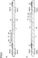
- Fig. 1(a) is a top view of the contactless communication medium, showing its internal structure
- Fig. 1(b) is a rear view thereof, according to the first embodiment of the present invention
- Fig. 2(a) is a cross-sectional view of the contactless communication medium shown in Fig. 1 , taken along the line IIa-IIa
- Fig. 2(b) is a cross-sectional view of the contactless communication medium shown in Fig. 1 , taken along the line IIb-IIb.
- Fig. 3 is a circuit diagram showing an equivalent circuit of the contactless communication medium shown in Fig. 1.
- Fig. 1(a) is a top view of the contactless communication medium, showing its internal structure
- Fig. 1(b) is a rear view thereof, according to the first embodiment of the present invention.
- Fig. 2(a) is a cross-sectional view of the contactless communication medium shown in Fig. 1 , taken along the line IIa-IIa
- the contactless communication medium is a contactless information medium capable of performing contactless communication with an external read/write device, such as a reader/writer, using signals primarily in the HF band, by applying RFID technology.
- a contactless communication medium 10 has a rectangular film base 11.
- On a top surface (a first surface) 11a of the film base 11 are an IC chip 12, an IC chip mounting portion 13, an antenna coil 14, a first inner plate electrode 15, and a first outer plate electrode 16.
- On a rear surface (a second surface) 11b of the film base 11 are a second inner plate electrode 17, a second outer plate electrode 18, and a jumper wire (a jumper portion) 19.
- the film base 11 is formed of materials having insulating properties and durability, for example, polyethylene naphthalate (PEN), polyethylene terephthalate copolymer (PET-G) and the like.
- PEN polyethylene naphthalate
- PET-G polyethylene terephthalate copolymer
- a metal foil is laminated to both the front and rear surfaces 11a and 11b of the film base 11. These metal foils are etched, for example, to form the IC chip mounting portion 13, the antenna coil 14, the first plate electrodes 15 and 16, the second plate electrodes 17 and 18, and the jumper wire 19.
- the IC chip 12 may be an IC chip for an IC tag storing ID information. Further, the IC chip 12 may be a module where an IC is mounted on a substrate and the like having terminals 12a and 12b.
- the IC chip 12 is mounted on the IC chip mounting portion 13 disposed at any location along a length of the antenna coil 14 on the top surface 11a of the film base 11.
- the IC chip mounting portion 13 has a pair of supporting portions 13a and 13b spaced from each other.
- the supporting portion 13a is connected to an inner end 14a of the antenna coil 14.
- the supporting portion 13b is connected to the first inner plate electrode 15.
- the terminals 12a and 12b disposed at the periphery of the IC chip 12 are joined to the pair of supporting portions 13a and 13b by ultrasonic welding and the like. Consequently, the IC chip 12 is connected to the antenna coil 14 via the IC chip mounting portion 13.
- the IC chip 12 may be mounted on the IC chip mounting portion 13 using other methods (for example, thermocompression bonding, adhesion by conductive adhesive, laser beam welding and the like).
- the IC chip 12 performs wireless communication processing via the conducted antenna coil 14, and sends and receives predetermined signals to and from an external read/write device
- the antenna coil 14 is a planar spiral antenna and is electromagnetically coupled to an antenna of an external read/write device such as a reader/writer in order to perform wireless communication.
- the number of turns of the antenna coil 14 is, for example, about 2 to 6.
- Fig. 1 shows an example with 4 turns, but the present invention is not limited to this.
- the width of each antenna wire constituting the antenna coil 14 is, for example, about 0.01 mm to 0.7 mm, more preferably about 0.02 mm to 0.6 mm. Further, the distance between the antenna wires constituting the antenna coil 14 is about 0.01 mm to 0.4 mm, more preferably about 0.02 mm to 0.3 mm. With this configuration, the antenna coil 14 sends and receives signals and receives power via wireless communication in a contactless manner.
- the antenna coil 14 is formed from a conductor disposed on the top surface 11a of the film base 11. Specifically, the antenna coil 14 is formed into a rectangular pattern by etching a copper foil or an aluminum foil having a thickness of 5 ⁇ m to 50 ⁇ m laminated on the top surface 11a side of the film base 11 having insulating properties which is made of, for example, polyethylene terephthalate (PET) or polyethylene naphthalate (PEN) having a thickness of 15 ⁇ m to 50 ⁇ m.
- PET polyethylene terephthalate
- PEN polyethylene naphthalate
- This antenna coil 14 is connected to the first outer plate electrode 16 at the outer end 14b.
- the antenna coil 14 is connected to the first inner plate electrode 15 at the inner end 14a via the IC chip mounting portion 13 and the IC chip 12.
- a first inner plate electrode 15 is a planar electrode formed inside the antenna coil 14 on the top surface 11 a of the film base 11.
- the first inner plate electrode 15 has a first electrode portion 15a extending along a long side direction (a first side direction) of the antenna coil 14, and a second electrode portion 15b extending along a short side direction (a second side direction) perpendicular to (intersecting) the long side direction of the antenna coil 14.
- the first electrode portion 15a and the second electrode portion 15b are each disposed adjacent to the inner periphery of the antenna coil 14 when viewed perpendicular to the film base 11.
- a first outer plate electrode 16 is a planar electrode formed outside the antenna coil 14 on the top surface 11a of the film base 11.
- the first outer plate electrode 16 has a first electrode portion 16a extending along the long side direction of the antenna coil 14, and a second electrode portion 16b extending along the short side direction of the antenna coil 14, thus forming an L-shape as a whole.
- the first electrode portion 16a and the second electrode portion 16b are each disposed adjacent to the outer periphery of the antenna coil 14 when viewed perpendicular to the film base 11. It is preferred that the first electrode portion 16a and the second electrode portion 16b be disposed adjacent to the antenna coil 14 such that a spacing S defined by the outer periphery of the antenna coil 14 is 0.5 mm or less as shown in Fig.
- plate electrodes 15, 17, 18 and the like be disposed such that the spacing S defined by the inner periphery or the outer periphery of the antenna coil 14 is 0.5 mm or less. This close arrangement provides the required number of turns of the antenna coil 14 and realizes suitable arrangements of the plate electrodes 15 to 18 while providing the opening located at the center of the contactless communication medium 10.
- the portion of the antenna coil 14 along which the first inner plate electrode 15 is disposed i.e., in the example of Fig. 1(a) , the upper edge and the right edge of the antenna coil 14
- the portion of the antenna coil 14 along which the first outer plate electrode 16 is disposed i.e., in the example of Fig. 1(a) , the left edge and the lower edge of the antenna coil 14. That is, the first inner plate electrode 15 and the first outer plate electrode 16 are disposed such that they do not share the same portions (edges) of the antenna coil 14.
- the first outer plate electrode 16 is disposed on the opposite side (i.e., point symmetrically) of the first inner plate electrode 15 with respect to a center point or a center line on the plane (surface 11a) of the film base 11.
- a symmetric arrangement also applies to the arrangement of a second inner electrode 17 and a second outer electrode 18 described later.
- the distance between the first inner plate electrode 15 and the inner periphery of the antenna coil 14, and the distance between the first outer plate electrode 16 and the outer periphery of the antenna coil 14, are, for example, substantially the same as the separation width at the same circumferential position within the antenna coil 14, and as described above, it is, for example, preferably 0.5 mm or less. However, the distance mentioned above may be greater than the separation width within the antenna coil 14, or may be less than the separation width.
- the first plate electrodes 15 and 16 are formed into a pattern by etching the metal foil laminated on the top surface 11a of the film base 11 similarly to the antenna coil 14. Second plate electrodes 17 and 18 and a jumper wire 19 described later are also similarly patterned by etching the metal foil laminated on the rear surface 11b of the film base 11.
- the second inner plate electrode 17 is a planar electrode paired with the first inner plate electrode 15, and is disposed on the rear surface 11b of the film base 11 so that it is opposite to the first inner plate electrode 15 in the thickness direction of the film base 11.
- the second inner plate electrode 17 has a first electrode portion 17a extending along the long side direction of the antenna coil 14, and a second electrode portion 17b extending along the short side direction of the antenna coil 14, thus forming an L-shape as a whole.
- the first and second electrode portions 17a and 17b are disposed opposite to the first and second electrode portions 15a and 15b of the first inner plate electrode 15 in the thickness direction of the film base 11.
- the first and second electrode portions 17a and 17b are disposed adjacent to the inner periphery of the antenna coil 14 when viewed perpendicular to the film base 11, similarly to the first and second electrode portions 15a and 15b of the first inner plate electrode 15.
- the second outer plate electrode 18 is a planar electrode paired with the first outer plate electrode 16, and is disposed on the rear surface 11b of the film base 11 so that it is opposite to the first outer plate electrode 16 in the thickness direction of the film base 11.
- the second outer plate electrode 18 has a first electrode portion 18a extending along the long side direction of the antenna coil 14, and a second electrode portion 18b extending along the short side direction of the antenna coil 14, to form an L-shape as a whole.
- the first and second electrode portions 18a and 18b are disposed opposite to the first and second electrode portions 16a and 16b of the first outer plate electrode 16 in the thickness direction of the film base 11. Therefore, the first and second electrode portions 18a and 18b are each disposed adjacent to the outer periphery of the antenna coil 14 when viewed perpendicular to the film base 11, similarly to the first and second electrode portions 16a and 16b of the first outer plate electrode 16.
- the first plate electrodes 15 and 16 and the second plate electrodes 17 and 18 each form a capacitance portion (see Fig. 3 ).
- the first plate electrodes 15 and 16 and the second plate electrodes 17 and 18 are disposed on the film base 11 such that the first plate electrodes 15 and 16 entirely cover the second plate electrodes 17 and 18 when viewed perpendicular to the film base 11.
- the jumper wire 19 is a wire that connects the second inner plate electrode 17 to the second outer plate electrode 18 on the rear surface 11b of the film base 11.
- the jumper wire 19 connects a tip portion of the second electrode portion 17b of the second inner plate electrode 17 to a side portion at the tip portion side of the first electrode portion 18a of the second outer plate electrode 18. It is preferred that the electrostatic capacitance between the jumper wire 19 and a portion of the antenna coil 14 opposite to the jumper wire 18 is low, and therefore it is preferred that the width is as small as possible (for example, about 1 to 3 mm).
- the jumper wire 19, disposed opposite to a portion of the antenna coil 14 in the thickness direction of the film base 11, is preferably formed perpendicular to the antenna coil 14.
- the term "perpendicular” does not only include the case where the antenna coil 14 and the jumper wire 19 intersect each other at right angles when viewed perpendicular to the film base 11 (or when viewed through the antenna forming surface of the film base 11), but also includes the case where they intersect each other at 90° plus or minus 10° (from 80° to 100°), which is a range permissible from a design perspective of.
- "disposed perpendicular to” mentioned above means that the antenna coil 14 and the jumper wire 19 are "perpendicular to each other" at least at a portion where they are intersecting each other, but it is not necessarily required that the entire jumper wire 19 be "perpendicular" to the antenna coil 14.
- the jumper wire 19 connects the second plate electrodes 17 and 18 so that the distance therebetween is the shortest. This in turn reduces resistance losses of the jumper wire 19.
- Such a jumper wire 19 allows an electrical connection between the second inner plate electrode 17 and the second outer plate electrode 18.
- the contactless communication medium 10 having such a configuration can be expressed as an equivalent circuit shown in Fig. 3 .
- the contactless communication medium 10 constitutes a circuit having the IC chip 12, the antenna coil 14, the first capacitance portion 16 and 18, the jumper wire 19, and the second capacitance portion 15 and 17 connected in series in that order.
- the pair of inner plate electrodes 15 and 17 consisting of the first inner plate electrode 15 and the second inner plate electrode 17 (namely, the pair of plate electrodes forming the second capacitance portion 15 and 17), and the pair of the outer plate electrodes 16 and 18 consisting of the first outer plate electrode 16 and the second outer plate electrode 18 (namely, the pair of plate electrodes forming the first capacitance portion 16 and 18) are arranged such that an electric current flows in the same direction as an electric current passing through the antenna coil 14.
- Such an arrangement is realized by providing the jumper wire 19 such that the electric current passing through the pair of outer plate electrodes 16 and 18, the jumper wire 19, and the pair of inner plate electrodes 15 and 17 flows in the same direction as the electric current passing through the antenna coil 14 when viewed perpendicular to the film base 11 (for example, clockwise or counterclockwise when viewed in the top surface 11a side of the film base 11).
- the electric current having flowed into the electrode portion 15a returns to the outer end 14b of the antenna coil 14 via the pair of inner plate electrodes 15 and 17, the jumper wire 19, and the pair of outer plate electrodes 16 and 18.
- the direction of the electric current flowing in that order is a clockwise direction as shown in the figure of Fig. 1(a) , and therefore conforms to the direction of the electric current passing through the antenna coil 14.
- capacitance portions capable of propagating high-frequency signals are formed by the first plate electrodes 15 and 16, and the second plate electrodes 17 and 18, which are respectively disposed on the surfaces 11a and 11b of the film base 11 so that they are opposite to each other .
- first plate electrodes 15 and 16, and the second plate electrodes 17 and 18 have the first electrode portions 15a, 16a, 17a, and 18a extending along the long side direction of the antenna coil 14, and the second electrode portions 15b, 16b, 17b, and 18b extending along the short side direction of the antenna coil 14 so that they are adjacent to the inner periphery or the outer periphery of the antenna coil 14 formed in a rectangular spiral shape when viewed perpendicular to the film base 11.
- This arrangement of the plate electrodes enables the contactless communication medium to have parallel plate electrodes and an opening of the antenna coil 14 (a region having no wiring pattern) under the constraints imposed by the limited outer dimensions of the contactless communication medium. More specifically, for example, as shown in Fig.
- an opening 11c having no antenna coil 14 is disposed in a central portion of the top surface 11a of the film base 11, and on the periphery, an antenna arranging region 11d, where the antenna coil 14 is to be arranged, is defined.
- the antenna coil 14 and the first plate electrodes 15 and 16 are disposed in the antenna arranging region 11d, and the region of the opening 11c covers about more than half of the entire area of the top surface 11a, which provides a sufficiently large opening.
- the IC chip mounting portion 13 and the IC chip 12 may be disposed in the opening 11c; however, unlike the antenna coil 14, these members are unlikely to pose problems when disposed in this position.
- the pair of inner plate electrodes 15 and 17, and the pair of outer plate electrodes 16 and 18 are arranged such that, when viewed perpendicular to the film base 11, the portion (edge) of the antenna coil 14 along which the pair of the inner plate electrodes 15 and 17 are disposed is different from the portion (edge) of the antenna coil 14 along which the pair of the outer plate electrodes 16 and 18 are disposed.
- the pair of inner plate electrodes 15 and 17 inside the antenna coil 14 and the pair of outer plate electrodes 16 and 18 outside the antenna coil 14 are arranged such that they do not share the same portions of the antenna coil 14.
- the pair of inner plate electrodes 15 and 17 and the pair of outer plate electrodes 16 and 18 are arranged such that they are not adjacent to each other and do not sandwich the same portion of the antenna coil 14 therebetween.
- the antenna coil 14, the pair of inner plate electrodes 15 and 17, and the pair of outer plate electrodes 16 and 18 are disposed on the film base 11 in a balanced manner.
- the antenna coil 14, and the plate electrodes 15, 16, 17, and 18 are appropriately arranged in an equally spaced and annular antenna pattern arrangement area as set according to a standard (for example, ISO/IEC 14443-1, Class 1) and the like.
- the effective number of coil turns has been increased by 1 due to the plate electrodes 15, 16, 17, and 18, and the jumper wire 19, and thus, the antenna coil 14 has an antenna function equivalent to that of the antenna coil 14 with 5 turns. Consequently, the number of turns (i.e., a region of an antenna pattern) required of the antenna coil 14 is reduced due to the effectively increased number of coil turns, thus increasing the area of the opening of the antenna coil 14.
- both the pair of inner plate electrodes 15 and 17, and the pair of outer plate electrodes 16 and 18 are disposed along two sides of the rectangular antenna coil 14.
- the pair of inner plate electrodes may be disposed along one side of the antenna coil 14 and the pair of outer plate electrodes may be disposed along the remaining three sides in a U-shape.
- the pair of outer plate electrodes may be disposed along one side of the antenna coil 14 and the pair of inner plate electrodes may be disposed along the remaining three sides of the antenna coil 14.
- a contactless communication medium 20 of the present embodiment differs from the contactless communication medium 10 of the first embodiment in that a jumper wire 21, connecting the second inner plate electrode 17 to the second outer plate electrode 18, connects a tip portion of the first electrode portion 17a of the second inner plate electrode 17 to a side portion near a tip portion of the second electrode portion 18b of the second outer plate electrode 18.
- the pair of inner plate electrodes 15 and 17, and the pair of outer plate electrodes 16 and 18 do not pass an electric current in the same direction as an electric current passing through the antenna coil 14.
- an electric current passing through the antenna coil 14 of the contactless communication medium 20 at a given instant will be described by providing an example case where the electric current passing through the antenna coil 14 flows from its outer end 14b toward its inner end 14a.
- the electric current passing through the antenna coil 14 flows from its outer end 14b in a clockwise direction, circles around several times (for example, 4 times in the present embodiment) along the antenna coil 14 in a rectangular shape, and flows into the electrode portion 15a of the first inner plate electrode 15 via the inner end 14a, the IC chip mounting portion 13, and the IC chip 12.
- the electric current flowing into the electrode portion 15a returns to the outer end 14b of the antenna coil 14 via the pair of inner plate electrodes 15 and 17, the jumper wire 19, and the pair of outer plate electrodes 16 and 18.
- the direction of the electric current flowing in this order is a counterclockwise direction as shown in Fig. 4(a) , and therefore does not conform to the direction of the electric current passing through the antenna coil 14.
- the pair of inner plate electrodes 15 and 17 and the pair of outer plate electrodes 16 and 18 do not function as radiating elements, but as capacitance portions.
- the contactless communication medium 20 has a structure similar to the contactless communication medium 10 of the first embodiment regarding points other than the above, and therefore produces effects similar to those of the contactless communication medium 10.
- FIG. 5(a) is a top view of a contactless communication medium, showing its internal structure, according to the third embodiment of the present invention, while Fig. 5(b) is a rear view thereof.
- Fig. 5(b) is a rear view thereof, where the top view shown in Fig. 5(a) is reversed about its central longitudinal axis.
- a contactless communication medium 30 of the present embodiment differs from the contactless communication medium 10 of the first embodiment in that, instead of not having the pair of outer plate electrodes 16 and 18, and the jumper wire 19, it has a conduction portion 31 for electrically connecting the outer end 14b of the antenna coil 14 and the second inner plate electrode 17.
- the conduction portion 31 is a wire extending from the tip portion of the first electrode portion 17a of the second inner plate electrode 17 to the position overlapping the outer end 14b of the antenna coil 14 in the thickness direction of the film base 11.
- the tip of the conduction portion 31 and the outer end 14b are connected to each other by caulking, welding and the like via a through hole disposed in the film base 11.
- the contactless communication medium 30 constitutes an equivalent circuit of a structure where the first capacitance portion 16 and 18, and the jumper wire 19 are replaced by the conduction portion 31 in the equivalent circuit shown in Fig. 3 .
- a capacitance portion capable of propagating high-frequency signals is formed of the first inner plate electrode 15 and the second inner plate electrode 17 respectively disposed on surfaces 11a and 11b of the film base 11 so as to be opposite to each other.
- the first inner plate electrode 15 and the second inner plate electrode 17 respectively have the first electrode portions 15a and 17a extending along the long side direction of the antenna coil 14, and the second electrode portions 16b and 18b extending along the short side direction of the antenna coil 14 so as to be adjacent to the inner periphery of the antenna coil 14 formed in a rectangular spiral shape when viewed perpendicular to the film base 11.
- the pair of outer plate electrodes 16 and 18, which are formed outside the antenna coil 14, are omitted among the plate electrodes constituting the contactless communication medium 10 of the first embodiment.
- the pair of inner plate electrodes 15 and 17 may be omitted instead of the pair of outer plate electrodes 16 and 18.
- the IC chip mounting portion 13 is disposed anywhere between the inner end 14a and the outer end 14b of the antenna coil 14, and a conduction portion is provided for electrically connecting the inner end 14a of the antenna coil 14 and the second outer plate electrode 18.
- Fig. 6(a) is a top view of a contactless communication medium, showing its inner structure, according to the fourth embodiment of the present invention, while Fig. 6(b) is a rear view thereof. Further, Fig. 6(b) is a rear view thereof, where the top view shown in Fig. 6(a) is reversed about its central longitudinal axis.
- a contactless communication medium 40 of the present embodiment a configuration that is primarily different from that of the contactless communication medium 10 of the first embodiment is hereinafter described.
- the contactless communication medium 40 has a first inner plate electrode 41 and a first outer plate electrode 42 formed inside and outside the rectangular antenna coil 14 on the top surface 11a of the film base 11.
- the first inner plate electrode 41 is disposed along the four sides of the antenna coil 14 so as to be adjacent to the inner periphery of the antenna coil 14. That is, the first inner plate electrode 41 is formed such that portions along each of the four sides of the antenna coil 14 are coupled to one another, and almost make a circle around the inner periphery of the antenna coil 14.
- the first inner plate electrode 41 has an electrode portion extending along each of the long side direction and the short side direction of the antenna coil 14 when viewed perpendicular to the film base 11.
- the first outer plate electrode 42 is disposed along the short side portion of the antenna coil 14 outside the antenna coil 14.
- the first outer plate electrode 42 consists of a rectangular first portion 42a covering more than half of the entire area, and 14 rectangular second portions 42b connected to a wiring pattern branched off from the central portion of the short side portion of the first portion 42a.
- the second portion 42b is smaller than the first portion 42a, and the portions are arranged in 2 rows, 7 pieces each.
- the contactless communication medium 40 has a second inner plate electrode 43 and a second outer plate electrode 44 formed on the inside and the outside of a rectangular shaped region (i.e., a region showing the antenna coil 14 by dashed lines in Fig. 6(b) corresponding to the antenna coil 14 on the rear surface 11b of the film base 11.
- the second inner plate electrode 43 is formed so as to be opposite to the first inner plate electrode 41 in the thickness direction of the film base 11.
- the second inner plate electrode 43 is arranged along the 4 sides of the rectangular shaped region so as to be adjacent to the inner periphery of the rectangular shaped region corresponding to the antenna coil 14, similarly to the first inner plate electrode 41.
- the second inner plate electrode 43 has an electrode portion extending along each of the long side direction and the short side direction of the antenna coil 14 when viewed perpendicular to the film base 11.
- the second outer plate electrode 44 is formed so as to be opposite to the first outer plate electrode 42 in the thickness direction of the film base 11.
- the second outer plate electrode 44 consists of a rectangular shaped first portion 44a covering half or more of the entire area, and 2 rectangular shaped second portions 44b connected to wiring patterns extending from both edges of a short side portion of the first portion 44a.
- the first portion 44a is arranged so as to be opposite to the first portion 42a of the first outer plate electrode 42 in the thickness direction of the film base 11.
- the second portion 44b is arranged so as to be opposite to 1 column (i.e., 7 pieces) of the second portions 42b of the first outer plate electrode 42 in the thickness direction of the film base 11.
- a terminal of the second inner plate electrode 43 and the first portion 44a of the second outer plate electrode 44 are connected with a jumper wire 45.
- a flow of an electric current passing through the antenna coil 14 of the contactless communication medium 40 at a given instant is hereinafter described by providing an example of the case where the electric current passing through the antenna coil 14 flows from its outer end 14b toward its inner end 14a.
- the electric current passing through the antenna coil 14 flows from its outer end 14b in a clockwise direction as shown in the figure, circles around the antenna coil 14 in a rectangular shape several times, (for example, 5 times in the present embodiment), and flows into the first inner plate electrode 41 via the inner end 14a, the IC chip mounting portion 13, and the IC chip 12.
- the electric current flowing into the first inner plate electrode 41 returns to the outer end 14b of the antenna coil 14 via the pair of the inner plate electrodes 41 and 43 consisting of the first inner plate electrode 41 and the second inner plate electrode 43, the jumper wire 45, and the pair of outer plate electrodes 42 and 44 consisting of the first outer plate electrode 42 and the second outer plate electrode 44.
- the pair of inner plate electrodes 41 and 43 are formed in a shape almost making a circle clockwise as shown in Fig. 6(a) in the inner circumference side of the antenna coil 14 along the 4 sides of the antenna coil 14 when viewed perpendicular to the film base 11. Therefore, the direction of the electric current passing through the pair of inner plate electrodes 41 and 43 conforms to the direction of the electric current passing through the antenna coil 14.
- the pair of inner plate electrodes 41 and 43 are arranged so as to pass the electric current along the same direction as the direction of the electric current passing through the antenna coil 14.
- the effective number of coil turns can be increased by having the pair of inner plate electrodes 41 and 43 function as a radiating element that passes the electric current in the same direction as the direction of the electric current passing through the antenna coil 14.
- the pair of outer plate electrodes 42 and 44 do not function as a radiating element, but purely function as a capacitance portion.
- the first inner plate electrode 41 and the second inner plate electrode 43 are arranged on the film base 11 such that the first inner plate electrode 41 entirely covers the second inner plate electrode 43 when viewed perpendicular to the film base 11.
- the first electrode portion 42a of the first outer plate electrode 42, and the first electrode portion 44a of the second outer plate electrode 44 are arranged on the film base 11 such that the first electrode portion 42a entirely covers the first electrode portion 44a when viewed perpendicular to the film base 11.
- the second electrode portion 42b of the first outer plate electrode 42, and the second electrode portion 44b of the corresponding second outer plate electrode 44 are arranged on the film base 11 such that the second electrode portion 42b entirely covers the second electrode portion 44b in the longitudinal direction of the film base 11 (a first direction parallel to the surface of the film base), and the second electrode portion 44b entirely covers the second electrode portion 42b in the transverse direction of the film base 11 (a second direction parallel to the surface of the film base and perpendicular to the first direction), when viewed perpendicular to the film base 11.
- the first inner plate electrode 41 and the second inner plate electrode 43 are arranged so as to be adjacent to the antenna coil 14 along the 4 sides of the antenna coil 14 when viewed perpendicular to the film base 11.
- This arrangement of the plate electrodes enables the contactless communication medium to have parallel plate electrodes and an opening of the antenna coil 14 under the constraints imposed by the limited outer dimensions of the contactless communication medium.
- Fig. 7(a) is a top view showing an internal structure of a contactless communication medium of the fifth embodiment of the present invention
- Fig. 7(b) is a rear view thereof.
- Fig. 7(b) shows a rear side view thereof, where the top view shown in Fig. 7(a) is reversed about its central longitudinal axis.
- a contactless communication medium 50 of the present embodiment is primarily different from the contactless communication medium 10 of the first embodiment in that the IC chip mounting portion 13 is arranged on the outside of the antenna coil 14 when viewed perpendicular to the film base 11, but is similar to the structure of the contactless communication medium 10 of the first embodiment regarding other aspects. Namely, although there are a few differences in size and position, the contactless communication medium 50 has first plate electrodes 51 and 52, and second plate electrodes 53 and 54 which is a structure similar to the first plate electrodes 15 and 16, and the second plate electrodes 17 and 18 in the contactless communication medium 10. Further, the contactless communication medium 50 has a jumper wire 55 connecting a second inner plate electrode 53 and a second outer plate electrode 54, similarly to the jumper wire 19 in the contactless communication medium 10.
- the IC chip mounting portion 13 is arranged along a corner of the top surface 11a of the film base 11.
- the antenna coil 14 and the first plate electrodes 51 and 52 are arranged along a corner facing, in a diagonal direction, a corner where the IC chip mounting portion 13 is arranged on the top surface 11a of the film base 11.
- one supporting portion 13a of the IC chip mounting portion 13 is connected to a second electrode portion 52b of the first outer plate electrode 52 via a predetermined wiring pattern.
- the other supporting portion 13b of the IC chip mounting portion 13 is connected to the outer end 14b of the antenna coil 14.
- the contactless communication medium 50 of the fifth embodiment it is possible to obtain effects similar to those produced by the contactless communication medium 10 of the first embodiment described above, and concurrently the area of the opening of the antenna coil 14 can be increased by arranging relatively large parts such as the IC chip mounting portion 13 and the IC chip 12 mounted on the IC chip mounting portion 13 not in the inside, but on the outside of the antenna coil 14.
- Fig. 8(a) is a top view showing an internal structure of a contactless communication medium of the sixth embodiment of the present invention
- Fig. 8(b) is a rear view thereof.
- Fig. 8(b) shows a rear side view thereof, where the top view shown in Fig. 8(a) is reversed about its central longitudinal axis.
- a contactless communication medium 60 of the present embodiment is primarily different from the contactless communication medium 40 of the fourth embodiment in that the IC chip mounting portion 13 is arranged on the outside of the antenna coil 14 when viewed perpendicular to the film base 11, but is similar to the structure of the contactless communication medium 40 of the fourth embodiment regarding other details. Namely, although there are a few differences in size and position, the contactless communication medium 60 has first plate electrodes 61 and 62, and second plate electrodes 63 and 64 which is a structure similar to the first plate electrodes 41 and 42, and the second plate electrodes 43 and 44 in the contactless communication medium 40. Further, the contactless communication medium 60 has a jumper wire 65 connecting a second inner plate electrode 63 and a second outer plate electrode 64, similarly to the jumper wire 45 in the contactless communication medium 40.
- the IC chip mounting portion 13 is arranged along a corner of the top surface 11a of the film base 11, similarly to the contactless communication medium 50 of the fifth embodiment.
- the antenna coil 14 and the first inner plate electrode 61 are arranged along a corner facing, in a diagonal direction, a corner where the IC chip mounting portion 13 is arranged on the top surface 11a of the film base 11.
- one supporting portion 13a of the IC chip mounting portion 13 is connected to a first electrode portion 62b of the first outer plate electrode 62 via a predetermined wiring pattern.
- the other supporting portion 13b of the IC chip mounting portion 13 is connected to the outer end 14b of the antenna coil 14.
- the contactless communication medium 60 of the sixth embodiment it is possible to obtain effects similar to those produced by the contactless communication medium 40 of the fourth embodiment described above, and concurrently the area of the opening of the antenna coil 14 can be increased by arranging relatively large parts such as the IC chip mounting portion 13 and the IC chip 12 mounted on the IC chip mounting portion 13 not in the inside, but on the outside of the antenna coil 14.
- the pair of outer plate electrodes 62 and 64 consisting of the first outer plate electrode 62 and the second outer plate electrode 64 are arranged along the outer periphery and the IC chip mounting portion 13 in the short side portion of the antenna coil 14 when viewed perpendicular to the film base 11.
- a space on the film base 11 where the first outer plate electrode 62 and the second outer plate electrode 64 are arranged is a space necessarily formed when the IC chip mounting portion 13 is arranged on the outside of the antenna coil 14.
- Fig. 9(a) is a top view showing an internal structure of a contactless communication medium of the seventh embodiment of the present invention
- Fig. 9(b) is a rear view thereof.
- Fig. 9(b) shows a rear side view thereof, where the top view shown in Fig. 9(a) is reversed about its central longitudinal axis.
- a contactless communication medium 70 of the present embodiment is different from the contactless communication medium 60 of the sixth embodiment in that it further has a first outer plate electrode 71, a second outer plate electrode 72, and a jumper wire 73, but is similar to the contactless communication medium 60 regarding other details.
- the first outer plate electrode 71 and the second outer plate electrode 72 are arranged along the outer periphery and the IC chip mounting portion 13 in the short side portion of the antenna coil 14 when viewed perpendicular to the film base 11. Further, the jumper wire 73 is branched off from the jumper wire 65, and connects the second outer plate electrode 72 and the second plate electrodes 63 and 64.
- the area of plate electrodes functioning as a capacitance portion can be further increased by arranging the plate electrodes (the first outer plate electrode 71 and the second outer plate electrode 72) while effectively using also a space necessarily formed on the outside of the long side portion of the antenna coil 14, and performance as a capacitance portion can be stabilized.
- a structure omitting the first outer plate electrode 62 and the second outer plate electrode 64, namely, a structure of arranging the plate electrodes while effectively using only a space necessarily formed in the outside of the long side portion of the antenna coil 14, may be employed.
- Fig. 10(a) is a top view showing an internal structure of a contactless communication medium of the eighth embodiment of the present invention
- Fig. 10(b) is a rear view thereof.
- Fig. 10(b) shows a rear side view thereof, where the top view shown in Fig. 10(a) is reversed about its central longitudinal axis.
- a contactless communication medium 80 of the present embodiment is different in shape from the contactless communication medium 10 of the first embodiment in that first plate electrodes 82 and 83, and second plate electrodes 84 and 85 are formed not in an "L" shape, but in a crescent shape, but is equivalent to the contactless communication medium 10 regarding its function as a circuit (which is to be described later in detail).
- the first inner plate electrode 82 is a crescent shaped planar electrode formed in the inside of an antenna coil 81 which is a pattern formed in a circle on the top surface 11a of the film base 11.
- the first inner plate electrode 82 is arranged along substantially half of the inner periphery of the antenna coil 81 (i.e., at least a third or more of the entire length of the inner circumference of the antenna coil 81), so as to be adjacent to the inner periphery of the antenna coil 81 when viewed perpendicular to the film base 11.
- the first outer plate electrode 83 is a crescent shaped planar electrode formed on the outside of the antenna coil 81 which is a pattern formed in a circle on the top surface 11a of the film base 11.
- the first outer plate electrode 83 is arranged along substantially half of the outer periphery of the antenna coil 81 (i.e., at least a third or more of the entire length of the outer circumference of the antenna coil 81), so as to be adjacent to the outer periphery of the antenna coil 81 when viewed perpendicular to the film base 11.
- a portion of the antenna coil 81 along which the first inner plate electrode 82 is arranged i.e., the left half of an arc portion of the antenna coil 81
- a portion of the antenna coil 81 along which the first inner plate electrode 82 is arranged i.e., the right half of the arc portion of the antenna coil 81 in an example of Fig. 10(a)
- the first inner plate electrode 82 and the first outer plate electrode 83 are arranged such that they do not share the same portions of the antenna coil 81 (the arc portion).
- the first outer plate electrode 83 is arranged on the opposite side (i.e., point symmetrically) to the first inner plate electrode 82 with respect to a center point or a center line on the plane (surface 11a) of the film base 11, similarly to the first embodiment and the like. Further, this holds true for the arrangement relation between the second inner plate electrode 84 and the second outer plate electrode 85 as described later.
- the second inner plate electrode 84 is a crescent-shaped planar electrode forming a pair with the first inner plate electrode 82, and is arranged on the rear surface 11b of the film base 11 so as to be opposite to the first inner plate electrode 82 in the thickness direction of the film base 11.
- the second inner plate electrode 84 extends along substantially half of the inner periphery of the antenna coil 81 (i.e., at least a third or more of the entire length of the inner circumference of the antenna coil 81) when viewed perpendicular to the film base 11, similarly to the first inner plate electrode 82.
- the second outer plate electrode 85 is a crescent-shaped planar electrode forming a pair with the first outer plate electrode 83, and is arranged on the rear surface 11b of the film base 11 so as to be opposite to the first outer plate electrode 83 in the thickness direction of the film base 11.
- the second outer plate electrode 85 extends along substantially half of the outer periphery of the antenna coil 81 (i.e., at least a third or more of the entire length of the outer circumference of the antenna coil 81) when viewed perpendicular to the film base 11, similarly to the first outer plate electrode 83.
- the second inner plate electrode 84 and the second outer plate electrode 85 are connected with a jumper wire 86.
- the first plate electrodes 82 and 83 and the second plate electrodes 84 and 85 form each of the 2 capacitance portions by arranging the first plate electrodes 82 and 83 and the second plate electrodes 84 and 85 to be opposite to each other.
- the first plate electrodes 82 and 83, and the second plate electrodes 84 and 85 are arranged on the film base 11 such that the first plate electrodes 82 and 83 entirely cover the second plate electrodes 84 and 85 when viewed perpendicular to the film base 11.
- the contactless communication medium 80 having such a structure constitutes an equivalent circuit of the contactless communication medium 10 shown in Fig. 3 , where the antenna coil 14 is replaced by the antenna coil 81, the first capacitance portions 15 and 17 are replaced by the capacitance portions 82 and 84 formed by the first inner plate electrode 82 and the second inner plate electrode 84, the jumper wire 19 is replaced by the jumper wire 86, and the second capacitance portions 16 and 18 is replaced by the capacitance portions 83 and 85 formed by the first outer plate electrode 83 and the second outer plate electrode 85.
- the contactless communication medium 80 is different from the contactless communication medium 10 of the first embodiment regarding the shape of each portion, but is equivalent thereto in the function as a circuit.
- the pair of inner plate electrodes 82 and 84 consisting of the first inner plate electrode 82 and the second inner plate electrode 84 (namely, the pair of plate electrodes forming the capacitance portions 82 and 84), and the pair of outer plate electrodes 83 and 85 consisting of the first outer plate electrode 83 and the second outer plate electrodes 85 (namely, the pair of plate electrodes forming the capacitance portion 83 and 85) are arranged so as to pass an electric current along the same direction as the direction of an electric current passing through the antenna coil 81.
- Such an arrangement is realized by setting up the jumper wire 86 such that the electric current passing through the pair of inner plate electrodes 82 and 84, the jumper wire 86, and the pair of outer plate electrodes 83 and 85 passes in the same direction as the direction of the electric current passing through the antenna coil 81 when viewed perpendicular to the film base 11 (for example, a clockwise or counterclockwise direction when viewed in the top surface 11a side of the film base 11).
- a flow of an electric current passing through the antenna coil 81 at a given instant is hereinafter described by providing an example of the case where the electric current passing through the antenna coil 81 flows from its outer end 81b toward its inner end 81a.
- the electric current passing through the antenna coil 81 flows from its outer end 81b in a counterclockwise direction as shown in the figure, circles around the antenna coil 81 in a circular shape several times, (for example, 4 times in the present embodiment), and flows into the first inner plate electrode 82 via the inner end 81a, the IC chip mounting portion 13, and the IC chip 12.
- the electric current flowing into the first inner plate electrode 82 returns to the outer end 81b of the antenna coil 81 via the pair of inner plate electrodes 82 and 84, the jumper wire 86, and the pair of outer plate electrodes 83 and 85.
- the direction of such electric current is a counterclockwise direction as shown in Fig. 10(a) , and therefore conforms to the direction of the electric current passing through the antenna coil 81.
- capacitance portions capable of propagating high-frequency signals are formed on both surfaces 11a and 11b of the film base 11 such that the first plate electrodes 82 and 83 and the second plate electrodes 84 and 85 are arranged disposed to each other.
- the first plate electrodes 82 and 83 and the second plate electrodes 84 and 85 are arranged along roughly half or more of the inner periphery or the outer periphery of the antenna coil 81 so as to be adjacent to the inner periphery or the outer periphery of the antenna coil 81 formed in a circular spiral shape when viewed perpendicular to the film base 11.
- This arrangement of the plate electrodes enables the contactless communication medium to have parallel plate electrodes and an opening of the antenna coil 81 under the constraints imposed by the limited outer dimensions of the contactless communication medium.
- the pair of inner plate electrodes 82 and 84 and the pair of outer plate electrodes 83 and 85 are arranged such that, when viewed perpendicular to the film base 11, the portion (an arc portion) of the antenna coil 81 along which the pair of inner plate electrodes 82 and 84 are arranged is different from the portion (an arc portion) of the antenna coil 81 along which the pair of outer plate electrodes 83 and 85 are arranged.
- the pair of inner plate electrodes 82 and 84 in the inside of the antenna coil 81, and the pair of outer plate electrodes 83 and 85 of the antenna coil 81 are arranged such that they do not share the same portions of the antenna coil 81.
- the pair of inner plate electrodes 82 and 84 and the pair of outer plate electrodes 83 and 85 are arranged such that they are not adjacent to each other and do not sandwich the same portion of the antenna coil 14 therebetween.
- the antenna coil 81, the pair of inner plate electrodes 82 and 84, and the pair of outer plate electrodes 83 and 85 can be arranged on the film base 11 with balance.
- the antenna coil 81, and the plate electrodes 82, 83, 84, and 85 can be appropriately arranged in an equally spaced and annular antenna pattern arrangement area as set in a standard (for example, ISO/IEC 14443-1, Class 1) and the like.
- the pair of inner plate electrodes 82 and 84, and the pair of outer plate electrodes 83 and 85 are arranged so as to pass an electric current along the same direction as the electric current passing through the antenna coil 81 as described above.
- the effective number of coil turns can be increased by having the pair of inner plate electrodes 82 and 84 and the pair of outer plate electrodes 83 and 85 function as radiating elements that pass an electric current along the same direction as the direction of an electric current passing through the antenna coil 81.
- the number of turns of the antenna coil 81 is 4.
- the effective number of coil turns is increased by 1 due to the plate electrodes 82, 83, 84, and 85, and the jumper wire 86, and an antenna function equivalent to that of the antenna coil 81 but having 5 turns can be provided.
- the number of turns namely, the area of an antenna pattern
- the area of the opening of the antenna coil 81 can be increased.
- present embodiment is illustrated by an example where the pair of inner plate electrodes 82 and 84 are arranged along substantially half of the inner periphery of the antenna coil 81 when viewed perpendicular to the film base 11, and the pair of outer plate electrodes 83 and 85 are arranged along substantially half of the outer periphery of the antenna coil 81 when viewed perpendicular to the film base 11.
- the pair of inner plate electrodes may be arranged along about more than half of the inner periphery of the antenna coil 81 when viewed perpendicular to the film base 11, while the pair of outer plate electrodes 83 and 85 may not be arranged along substantially half of the outer periphery of the antenna coil 81 when viewed perpendicular to the film base 11.
- the pair of outer plate electrodes 83 and 85 may be arranged along about more than half of the outer periphery of the antenna coil 81 when viewed perpendicular to the film base 11, while the pair of inner plate electrodes may not be arranged along about more than half of the inner periphery of the antenna coil 81 when viewed perpendicular to the film base 11. Namely, it is only necessary that at least one of the pair of inner plate electrodes and the pair of outer plate electrodes are arranged along about more than half of the inner periphery or the outer periphery of the antenna coil 81.
- the shape of the antenna coil 81 may not be a circular shape, but an elliptic shape, or it may have a polygonal shape. In the case of using an antenna coil having such a shape other than a circular shape, a structure of a contactless communication medium based on the idea similar to the content described in the present embodiment may be adopted.
- Fig. 11(a) is a top view showing an internal structure of a contactless communication medium of a ninth embodiment of the present invention
- Fig. 11(b) is a rear view thereof.
- Fig. 11(b) shows a rear side view thereof, where the top view shown in Fig. 11(a) is reversed about its central longitudinal axis.
- a contactless communication medium 90 of the present embodiment is primarily different from the contactless communication medium 80 of the eighth embodiment in that the IC chip mounting portion 13 is arranged on the outside of the antenna coil 81 when viewed perpendicular to the film base 11.
- the contactless communication medium 90 is primarily different from the contactless communication medium 80 of the eighth embodiment in that the pair of crescent-shaped inner plate electrodes 82 and 84 are replaced by a pair of inner plate electrodes 92 and 94 formed along nearly the entire inner circumference of the antenna coil 81 when viewed perpendicular to the film base 11
- the first inner plate electrode 92 is arranged along nearly the entire inner periphery of the antenna coil 81 so as to be adjacent to the inner periphery of the antenna coil 81 when viewed perpendicular to the film base 11.
- the first outer plate electrode 93 is arranged along substantially half of the outer periphery of the antenna coil 81 so as to be adjacent to the outer periphery of the antenna coil 81 when viewed perpendicular to the film base 11, similarly to the first outer plate electrode 83 in the contactless communication medium 80 of the eighth embodiment.
- the second plate electrodes 94 and 95 are formed on the rear surface 11b of the film base 11 so as to be opposite to the first plate electrodes 92 and 93 in the thickness direction of the film base 11.
- the second inner plate electrode 94 and the second outer plate electrode 95 are connected with a jumper wire 96.
- a flow of an electric current passing through the antenna coil 81 of the contactless communication medium 90 at a given instant is hereinafter described by providing an example of the case where the electric current passing through the antenna coil 81 flows from its outer end 81b toward its inner end 81a.
- the electric current passing through the antenna coil 81 flows from its outer end 81b in a counterclockwise direction as shown in the figure, circles around the antenna coil 81 in a circular shape several times, (for example, 4 times in the present embodiment), and flows into the first inner plate electrode 92 from the inner end 81a.
- the electric current flowing into the first inner plate electrode 92 returns to the outer end 14b of the antenna coil 14 via the pair of inner plate electrodes 92 and 94, the jumper wire 96, and the pair of outer plate electrodes 93 and 95.
- the pair of inner plate electrodes 92 and 94 are formed in a shape almost making a circle counterclockwise, as shown in Fig. 11(a) , along the inner periphery of the antenna coil 81 when viewed perpendicular to the film base 11. Therefore, the direction of the electric current passing through the pair of inner plate electrodes 92 and 94 conforms to the direction of the electric current passing through the antenna coil 81.
- the pair of inner plate electrodes 92 and 94 are arranged so as to pass the electric current in the same direction as the direction of the electric current passing through the antenna coil 81.
- the effective number of coil turns can be increased by having the pair of inner plate electrodes 92 and 94 function as a radiating element that passes an electric current along the same direction as the direction of an electric current passing through the antenna coil 81.
- the pair of outer plate electrodes 93 and 95 do not function as a radiating element, but purely function as a capacitance portion.
- the contactless communication medium 90 of the ninth embodiment it is possible to increase the area of the opening of the antenna coil 81 by arranging relatively large parts such as the IC chip mounting portion 13 and the IC chip 12 mounted on the IC chip mounting portion 13 not in the inside, but on the outside of the antenna coil 81.
- the contactless communication medium of the present embodiment may be as described above, but the contactless communication medium of the present invention is not limited to the embodiment described above, and various modifications can be applied.
- the structure of each portion described in the first to ninth embodiments described above can be adequately combined in aspects other than the combinations adopted in the embodiments described above.
- the contactless communication media described above may include not only a contactless IC card, but also, for example, contactless communication media such as an electronic passport and the like, and are not particularly limited. The same holds true for the following modifications.
- the film base 111 is a base made up of dielectric and having, for example, a triple-layer structure, and has a structure having an intermediate base 111c as the main base having insulating properties and durability such as polyethylene naphthalate (PEN), polyethylene terephthalate copolymer (PET-G) and the like.
- PEN polyethylene naphthalate
- PET-G polyethylene terephthalate copolymer
- first and second dielectric layers 111d and 111 e having a smaller thickness than that of the intermediate base 111c, are provided for adjustment. Further, details of the first and second dielectric layers 111d and 111e will be described later.
- a metal foil is laminated on both the front and rear surfaces 111a and 111b of the film base 111 prior to processing by etching and the like, and the antenna coil 113, the first plate electrodes 114a and 114b, the second plate electrodes 116a and 116b, and the jumper wire 117 are formed by processing the metal foil such as by etching.
- the metal foil arranged on each of the front and rear surfaces 111a and 111b of the film base 111 may have the same thickness, or the thickness of the metal foil on the top surface 111a side where the antenna coil 113 is arranged may be made larger than the thickness of the metal foil on the rear surface 111b side where the second plate electrodes 116a and 116b are arranged, since the antenna coil 113 is arranged with a small pitch and the electrical resistance of the antenna coil 113 needs to be reduced. Further, such a three-layer structure may obviously be applied to the contactless communication medium 10 and the like of the first embodiment to the ninth embodiment described above.
- the IC chip 112 is constituted by an IC tag storing, for example, ID information.
- the IC chip 112 is arranged along a length of the antenna coil antenna coil 113 on the top surface 111a of the film base 111, and both its terminals are connected to the antenna coil 113.
- the IC chip 112 performs wireless communication processing via the conducted antenna coil 113, and sends and receives predetermined signals to and from an external read/write device.
- the antenna coil 113 is a plane spiral shaped antenna for performing contactless wireless communication by electromagnetically coupling with an antenna of an external read/write device such as a reader/writer.
- the antenna coil 113 sends and receives signals and receives power by wireless communication in a contactless state.
- the antenna coil 113 is formed from a conductor (metal foil) arranged on the top surface 111a of the film base 111.
- the antenna coil 113 is patterned, for example, by etching a copper foil or an aluminum foil having a thickness of 5 ⁇ m to 50 ⁇ m laminated on the top surface 111a side of the film base 111 having a thickness of 15 ⁇ m to 50 ⁇ m.
- Such an antenna coil 113 is connected to the plate electrode 114a at its outer end, and is connected to the plate electrode 114b at its inner end.
- the first plate electrodes 114a and 114b are each a rectangular shaped plate electrode, and are arranged in parallel at one side of the top surface 111a of the film base 111 sandwiching a portion of the antenna coil 113 therebetween.
- the plate electrode 114b is formed in the inside of the antenna coil 113, and therefore its electrode area is smaller than that of the plate electrode 114a.
- the electrode areas of plate electrodes 114a and 114b may be the same, or the electrode area of the plate electrode 114b may be larger than that of the plate electrode 114a.
- the plate electrode 114a is connected to the outer end of the antenna coil 113 as described above, and the plate electrode 114b is connected to the inner end of the antenna coil 113.
- first plate electrodes 114a and 114b are patterned by etching the metal foil laminated on the top surface 111a side of the film base 111 similarly to the antenna coil 113.
- the second plate electrodes 116a and 116b, and the jumper wire 117 to be described later are also similarly formed.
- the second plate electrodes 116a and 116b are each a rectangular plate electrode, and are arranged in parallel at one side of the rear surface 111b of the film base 111, with a portion of the region corresponding to the antenna coil 113 located therebetween.
- the plate electrode 116b is formed in the inside of the region corresponding to the antenna coil 113 (region of the antenna coil 113 shown by dotted lines in Fig. 13(b) ), and therefore its electrode area is smaller than that of the plate electrode 116a, which is, however, not limited, similarly to the first plate electrodes 114a and 114b. Further, as shown in Fig. 14(a) and Fig.
- the second plate electrodes 116a and 116b are formed so as to be opposite to the first plate electrodes 114a and 114b in the thickness direction of the film base 111. More specifically, the plate electrode 114a and the plate electrode 116a are opposite to each other, and the plate electrode 114b and the plate electrode 116b are opposite to each other. With such an arrangement, the first plate electrodes 114a and 114b, and the second plate electrodes 116a and 116b each form 2 capacitance portions (see Fig. 15 ).
- plate electrodes 114a and 116a opposite to each other have the same shape and the same size (area), and plate electrodes 114b and 116b opposite to each other similarly have the same shape and the same size. Further, each plate electrode of these first plate electrodes 114a and 114b, and the second plate electrodes 116a and 116b are in conformity when viewed perpendicular to the film base 111. Further, the second plate electrodes 116a and 116b, unlike the first plate electrodes 114a and 114b, are not connected to the antenna coil 113.
- the jumper wire 117 is a wire which connects the second plate electrodes 116a and 116b on the rear surface 11b of the film base 111.
- the jumper wire 117 preferably has a small electrostatic capacitance between it and a portion of the antenna coil 113 opposite to the jumper wire 117, and therefore its width is preferably as small as possible, for example, in the order of 1 to 3 mm.
- the jumper wire 117 is connected to the plate electrodes 116a and 116b in the long side direction of the plate electrodes 116a and 116b shown in the upper portion of the figure, but it may be connected at other portions such as a central portion.
- the contactless communication medium 110 having such a structure can be expressed as an equivalent circuit as shown in Fig. 15 .
- the contactless communication medium 110 is constituted by a circuit having the IC chip 112, the antenna coil 113, the first capacitance portion 114a and 116a, the jumper wire 117, and the second capacitance portion 114b and 116b arranged in this order.
- a layer structure of the film base 111 of the contactless communication medium 110 having such a structure, and effects and functions produced thereby will be further described in detail with reference to Fig. 14(a) and Fig. 14(b) .
- the film base 111 constituting the contactless communication medium 110 has a three-layer structure having, in addition to the intermediate base 111c which is the primary base, a first dielectric layer for adjustment 111d comprising dielectric and formed on a surface of the intermediate base 111c shown in the upper portion of the figure, and a second dielectric layer for adjustment 111e comprising dielectric and formed on a surface of the intermediate base 111c shown in the lower portion of the figure.
- the reason that the film base 111 has such a three-layer structure in the contactless communication medium 110 of the present modification is to enable adjustment by simple means of the electrostatic capacitance values of the capacitance portion (capacitor) formed by the first and second plate electrodes 114a and 116a, and the capacitance portion (capacitor) formed by the first and second plate electrodes 114b and 116b, by adjusting the thickness, dielectric constant and the like of the first and second dielectric layers 111d and 111e.
- the first and second dielectric layers 111d and 111e are layers for adjusting the electrostatic capacitance value, and from the perspective of making the contactless communication medium 110 thinner, it is preferable that it is thinner than the thickness of the intermediate base 111c, which is not limited.
- the dielectric material constituting the first and second dielectric layers 111d and 111e may be constituted by a different material from a dielectric material of the intermediate base 111c, for example, comprising PET and the like, but may be constituted by the same material.
- a material constituting the first and second dielectric layers 111d and 111e includes, for example, polyester-based resin, polyether-based resin, polyethylene, polypropylene, EVA resin and the like.
- the first and second dielectric layers 111d and 111e may be formed by coating such dielectric material on both the front and rear surfaces of the intermediate base 111 c, followed by curing.
- the thicknesses and the materials used (i.e., dielectric constant) of the first and second dielectric layers 111d and 111e can be adequately adjusted.
- the film base 111 of such a three-layer structure may obviously be adopted in the structure of the film base 111 used in the first embodiment to the ninth embodiment described above, and by adopting the structure of the film base 111 in the film base 11, it is possible to similarly produce the same functions, effects and the like to be described later in the contactless communication medium and the like of the first embodiment to the ninth embodiment.
- the film base 111 sandwiched between the first plate electrodes 114a and 114b and the second plate electrodes 116a and 116b has a three-layer structure having the intermediate base 111c, and the first and second dielectric layers 111d and 111e.
- the thickness of the film base 111 comprising the dielectric namely the separation distances between the first and second plate electrodes 114a and 116a, and between 114b and 116b can be easily adjusted, for example, by changing the thickness of the first and second dielectric layers 111d and 111e, and it is possible to easily adjust the capacitances of the capacitors made of the first and second plate electrodes 114a, 114b, 116a, and 116b without changing the shapes (areas) and the like of the electrode pattern of the plate electrodes 114a, 114b, 116a, and 116b constituting the capacitors.
- the structure is such that conduction is achieved with capacitors formed between the first plate electrodes 114a and 114b connected to the antenna coil 113, and the second plate electrodes 116a and 116b arranged on the rear surface side, and therefore production and inspection processes can be simplified and connection reliability can be improved compared to the case where the start end and the finish end of the antenna coil 113 are directly connected to a conductor pattern on the rear surface side.
- the dielectric constants of the dielectrics constituting the first and second dielectric layers 111d and 111e are equivalent to or more than the dielectric constant of the dielectric constituting the intermediate base 111c. Therefore, even when the layer thicknesses of the first and second dielectric layers for adjustment 111d and 111e are small, the capacitances of the capacitors made of the first and second plate electrodes 114a, 114b, 116a, and 116b can be easily adjusted.
- the thicknesses of the first and second dielectric layers 111d and 111e are smaller than the thickness of the intermediate base 111c.
- the dielectric layers for adjustment for adjusting the capacitances of the capacitors made of the first and second plate electrodes 114a, 114b, 116a, and 116b can be made thin, and therefore it is possible to control the variance in total thickness of the film base 111 in each product. Further, the whole contactless communication medium 110 can be made thinner.
- the first and second dielectric layers 111d and 111e are formed by coating a predetermined dielectric material on the intermediate base 111c, followed by curing.
- the thicknesses, dielectric constants and the like of the first and second dielectric layers 111d and 111e can be easily adjusted, and therefore it is possible to easily adjust the capacitances of the capacitors made of the first and second dielectric layers 114a, 114b, 116a, and 116b.
- the thickness of the metal foil constituting the antenna coil 113 is larger than the thickness of the metal foil constituting the second plate electrode 116a and 116b. As such, electrical resistance in the antenna coil 113 can be reduced, and it is possible to improve the radiation efficiency of the antenna of the contactless communication medium 110. Further, this structure may be adopted in the structure of the contactless communication medium used in the first embodiment to the ninth embodiment of the present invention described above.
- the area in the plane of the second plate electrode 116a arranged on the rear surface 111b side may be larger than the area in the plane of the first plate electrode 114a, and that, when viewed in a direction perpendicular to the plane of the first and second plate electrodes 114a and 116a, the first plate electrode 114a may be surrounded by the second plate electrode 116a.
- a position and the like of both plate electrodes 114a and 116a may be somewhat misaligned from designed values due to production errors and the like.
- the area in the plane of the first plate electrode 114a may be larger than the area in the plane of the second plate electrode 116a, and that, when viewed perpendicular to the plane of the first and second plate electrodes 114a and 116a, the second plate electrode 116a may be surrounded by the first plate electrode 114a.
- the antenna coil 113 is also formed on the same side as the first plate electrode 114a, and therefore, by making the size of the second plate electrode 116a larger, the contactless information medium 110 as a whole is likely to be downsized. Further, a relation between areas of the first and second plate electrodes 114a and 116a was described above, but the same holds true for a relation between areas of the first and second plate electrodes 114b and 116b.
- Fig. 19 is a cross sectional view schematically showing a flow of an electric current between plate electrodes of the contactless communication medium shown in Fig. 18(a) and (b).
- Fig. 20 is a circuit diagram showing an equivalent circuit of the contactless communication medium shown in Fig. 18(a) and (b).
- the contactless communication medium 110a has the film base 111, the IC chip 112, the antenna coil 113, the first plate electrodes 114a and 114b, the second plate electrodes 116a and 116b, and the jumper wire 117, similarly to the first modification.
- plate electrodes 114a, 114b, 116a, and 116b are formed on a flow path of an electric current passing through the antenna coil 113 and constituting a portion of a coil pattern.
- the plate electrodes 114a, 114b, 116a, and 116b are included in the coil pattern including the antenna coil 113, and therefore, for example as shown in Fig. 19 , an electric current passes from the plate electrode 114b to the plate electrode 116b across the film base 111.
- the electric current passes along the travelling direction indicated by arrows in the figure, and therefore the amount of electric current passing through the first plate electrode 114b is larger than the amount of electric current passing through the second plate electrode 116b in region ⁇ , whereas the amount of electric current passing through the second plate electrode 116b is larger than the amount of electric current passing through the first plate electrode 114b in region ⁇ .
- the relation between the amounts of electric currents holds true between the planar electrodes 114a and 116a.
- an average electric current density in an electrode cross section of each of the plate electrodes 114a, 114b, 116a, and 116b may be used as an index in place of the amount of electric current, similarly to the case of using the amount of electric current.
- the plate electrodes 114a, 114b, 116a, and 116b can be used as a portion of the antenna, and under the limited antenna forming region, it is possible to increase the number of coil turns and concurrently enlarge the opening area of the antenna. Further, an equivalent circuit of such a contactless communication medium 110a is shown in Fig. 20 .
- the plate electrode 114b may be shaped such that one side is a broad portion 114c and the other side is a thin portion 114d as shown in Fig. 21(a)
- the plate electrode 116b may be shaped such that one side is a thin portion 116c and the other side is a broad portion 116d as shown in Fig. 21(b) . In this case, as shown in Fig.
- the area of the first plate electrode 114b (114c) is larger than the area of the second plate electrode 116b (116c).
- the area of the second plate electrode 116b (116d) is larger than the area of the first plate electrode 114b (114d).
- the area of the second plate electrode 116b is larger than the area of the first plate electrode 114b. Therefore, it is possible to enlarge the forming region of another member such as the antenna coil 113 and the like similarly as described above. Further, also in the case of the second modification, this structure may be adequately applied in the structures of the contactless communication medium of the first embodiment to the ninth embodiment described above similarly to the first modification.
- the film base 111 is constituted by a three-layer structure.
- the present invention is not limited to a three-layer structure, and the film base 111 may be formed from a structure having 4 or more layers, each comprising a dielectric. In this case, it is possible to more finely adjust the capacitances of the capacitors constituted by the first and second plate electrodes 114a, 114b, 116a, and 116b.
- the present invention provides a contactless information medium having parallel plate electrodes and designed to have an opening of an antenna coil.
Description
- The present invention relates to a contactless information medium.
-
Patent Document 1 discloses an example of an RFID medium (a contactless information medium) such as a contactless IC card which performs wireless communication using signals in an HF band (for example, 13.56 MHz). An antenna pattern of an antenna coil of such an RFID medium can be designed in any shape as long as functional requirements for performing wireless communications with external devices are met. - Certain restrictions may be imposed on the antenna pattern in order to meet the requirements of a shape or a specific standard of an object to which the RFID medium is to be installed. For example, in the standard specified as ISO/IEC 14443-1,
Class 1, an area where an antenna pattern can be arranged is set in order to provide an opening (a region having no wiring pattern) formed inside an antenna coil. Specifically, in the above standard, the area where the antenna pattern can be arranged is set to be an annular area obtained by removing, from a rectangular region having a length of 49 mm and a width of 81 mm, a substantially rectangular region having a length of 34 mm and a width of 64 mm (this rectangular region having corners rounded with R3 mm) and centered in the rectangular region. - Patent Document 2 describes a resonance circuit including a front-side coil-shaped conductor and a back-side coil-shaped conductor in cuboid shapes, which are arranged on the front and back surfaces of a dielectric sheet so as to be opposed to each other. Coil-shaped conductors are respectively wound from first ends to second ends and coupled with capacitance interposed therebetween so as to be opposed to each other. In the coil-shaped conductors, the opposed section is equal or substantially equal in conductor width, and the outermost windings and the innermost windings are preferably configured in a line shape, and each arranged so that two sides are thicker in conductor width than any other winding.
-
Patent Document 3 describes an integrated circuit device including a contactless integrated circuit inlay. The inlay includes a substrate. A passive integrated circuit chip is adhesively attached to a first surface of substrate. -
- Patent Document 1:
JP 2004-355442 A - Patent Document 2:
US 2013/135172 A1 - Patent Document 3:
US 2009/108974 A1 - In such an RFID medium, a capacitance portion capable of propagating high-frequency signals using parallel plate electrodes may be provided in a circuit. In that case, a wiring pattern to connect the parallel plate electrodes to an antenna coil is necessary, and therefore it may be difficult to meet the requirements of the above standard. For example, when parallel plate electrodes are disposed substantially centrally in an opening formed inside an antenna coil as with the examples disclosed in
Patent Document 1, the requirements of the above standard cannot be met. Further, when the requirements of the above standard are not met and the area of the opening of the antenna coil is insufficient, the radiation efficiency of the antenna may decrease, and therefore it is recommended that the wiring pattern be preferably accommodated within the annular area as set according to the above standard to provide the opening of the antenna coil. - To solve the problem above, an object of the present invention is to provide a contactless information medium having parallel plate electrodes and designed to have an opening of an antenna coil.
- This object is accomplished by the contactless information medium defined in
claim 1. The dependent claims concern particular embodiments. - According to an aspect of the present invention, the contactless information medium includes a film base, an antenna coil, an IC chip, a first plate electrode, and a second plate electrode. The antenna coil is disposed on a first surface of the film base, and formed in a spiral shape to perform wireless communication with an external device. The IC chip is disposed on the first surface of the film base, connected to the antenna coil via an IC chip-mounted portion, and performs wireless communication processing via the antenna coil. The first plate electrode is disposed on the first surface of the film base, and connected to at least one of an inner end and an outer end of the antenna coil. The second plate electrode is disposed on a second surface of the film base so as to be opposite to the first plate electrode in the thickness direction of the film base. Further, in the contactless information medium, each of the first plate electrode and the second plate electrode has a first electrode portion and a second electrode portion. The first electrode portion and the second electrode portion respectively extend along a first side direction of the antenna coil and a second side direction intersecting with the first side direction so that the first and second electrode portions are adjacent to an inner periphery or an outer periphery of the antenna coil when viewed perpendicular to the film base. Alternatively, the first and second plate electrodes are disposed along greater than or equal to one-third of the entire length of the inner periphery or the outer periphery of the antenna coil so as to be adjacent to the inner periphery or the outer periphery of the antenna coil when viewed perpendicular to the film base.
- In the contactless information medium, the first plate electrode has a first inner plate electrode connected to the inner end of the antenna coil, and a first outer plate electrode connected to the outer end of the antenna coil. The second plate electrode has a second inner plate electrode opposite to the first inner plate electrode in the thickness direction of the film base, and a second outer plate electrode opposite to the first outer plate electrode in the thickness direction of the film base. The first outer plate electrode is disposed on the opposite side of the first inner plate electrode with respect to a center point or center line on the plane of the film base. In that case, the first plate electrode and the like are arranged well-balanced on the surface of the film base, enabling the contactless information medium to have parallel plate electrodes and an opening of the antenna coil under the constraints imposed by the limited outer dimensions of the contactless information medium.
- The contactless information medium further includes a jumper portion connecting the second inner plate electrode to the second outer plate electrode on the second surface of the film base. With the second inner plate electrode connected to the second outer plate electrode with the jumper portion, the second inner plate electrode and the second outer plate electrode are disposed on opposite sides of the film base without the plate electrodes directly connecting to each other, and a capacitance portion capable of propagating high-frequency signals can be provided in a circuit. This enables an electrical connection between electrodes to be made with greater reliability because propagation of signals by the capacitance portion will not be disturbed even if the film base expands when heated.
- In the contactless information medium, the first plate electrode may have a first inner plate electrode connected to the inner end of the antenna coil, and a first outer plate electrode connected to the outer end of the antenna coil. The second plate electrode may have a second inner plate electrode opposite to the first inner plate electrode in the thickness direction of the film base, and a second outer plate electrode opposite to the first outer plate electrode in the thickness direction of the film base. Each of the first inner plate electrode and the first outer plate electrode may have the first electrode portion and the second electrode portion. In this case, the first plate electrode and the like are arranged well-balanced on the surface of the film base, thus enabling the contactless information medium to have parallel plate electrodes and an opening of the antenna coil, under the constraints imposed by the limited outer dimensions of the contactless information medium.
- In the contactless information medium, the pair of inner plate electrodes consisting of the first inner plate electrode and the second inner plate electrode, and the pair of outer plate electrodes consisting of the first outer plate electrode and the second outer plate electrode may be arranged such that, when viewed perpendicular to the film base, a portion of the antenna coil along which the pair of the inner plate electrodes are disposed is different from a portion of the antenna coil along which the pair of the outer plate electrodes are disposed. In that case, the pair of the inner plate electrodes inside the antenna coil, and the pair of the outer plate electrodes outside the antenna coil are arranged such that they do not share the same portions of the antenna coil. In other words, the pair of the inner plate electrodes and the pair of the inner plate electrodes are arranged so that the two pairs do not adjoin each other and do not sandwich the same portion of the antenna coil therebetween. Thus, the antenna coil, the pair of the inner plate electrodes, and the pair of the outer plate electrodes are disposed on the film base in a balanced manner. Specifically, the antenna coil and the plate electrodes can be adequately arranged in an equally spaced and annular antenna pattern arranging area defined in a standard (for example, ISO/IEC 14443-1, class 1) and the like.
- In the contactless information medium, at least one of the pair of inner plate electrodes consisting of the first inner plate electrode and the second inner plate electrode, and the pair of outer plate electrodes consisting of the first outer plate electrode and the second outer plate electrode may be arranged such that an electric current flows in the same direction as an electric current passing through the antenna coil. The number of coil turns can be effectively increased by enabling at least one of the pair of inner plate electrodes and the pair of outer plate electrodes to function as a radiating element that passes an electric current in the same direction as an electric current passing through the antenna coil. Thus, it is possible to reduce the number of turns (that is, the area of the antenna pattern) required of the antenna coil due to the number of coil turns effectively increased, thereby increasing the area of the opening of the antenna coil.
- In the contactless information medium, the antenna coil has any one of a circular shape, an elliptic shape, and a polygonal shape including a rectangular shape.
- In the contactless information medium, the IC chip mounting portion may be disposed outside the antenna coil when viewed perpendicular to the film base. When relatively large parts such as the IC chip mounting portion and the IC chip mounted on the IC chip mounting portion are disposed outside the antenna coil, the area of the opening of the antenna coil can be increased.
- In the contactless information medium, the IC chip mounting portion may be disposed outside the antenna coil when viewed perpendicular to the film base, and the pair of outer plate electrodes consisting of the first outer plate electrode and the second outer plate electrode may be disposed, when viewed perpendicular to the film base, along the outer periphery of the antenna coil and the IC chip mounting portion. In that case, the plate electrodes can be disposed by effectively using an empty space outside the antenna coil on the film base.
- In the contactless information medium, the first and second plate electrodes may be disposed on the film base such that one of the plate electrodes entirely covers the other plate electrode when viewed perpendicular to the film base. Further, in the contactless information medium, the first and second plate electrodes may be disposed on the film base such that, when viewed perpendicular to the film base, one of the plate electrodes entirely covers the other plate electrode in the first direction parallel to the surface of the film base, and the latter plate electrode entirely covers the former plate electrode in the second direction parallel to the surface of the film base and perpendicular to the first direction. With this arrangement of the plate electrodes, even if the second plate electrode is misaligned from the first plate electrode due to manufacturing tolerances and the like, capacitance of the parallel plates formed by the electrodes will not change, which reduces variations in electric characteristics of products.
- In the contactless information medium, an antenna arranging region having a frame shape, where the antenna coil is disposed, is defined on the periphery of the first surface of the film base. The antenna arranging region may be located between the outer periphery of the film base and an antenna non-arranging region that covers about more than half of the entire area of the first surface and that is defined in the center of the first surface. Defining such an antenna arranging region enables the contactless information medium to have parallel plate electrodes and a required opening of the antenna coil (an antenna non-arranging region), under the constraints imposed by the limited outer dimensions of the contactless information medium.
- In the contactless information medium, the first plate electrode may be disposed adjacent to the closest antenna coil such that the space between the first plate electrode and the inner periphery or the outer periphery of the antenna coil is 0.5 mm or less. This allows the first plate electrode and the antenna coil to be arranged with greater efficiency.
- In the contactless information medium, the film base may include an intermediate base formed of a dielectric, a first dielectric layer for adjustment formed of a dielectric and formed on a first surface of the intermediate base, and a second dielectric layer for adjustment formed of a dielectric and formed on a second surface of the intermediate base. With such a three-layer structure, the thickness of the film base formed of dielectric material, namely the distance between the first and second plate electrodes, can be easily adjusted, for example, by changing the thickness of the first or second dielectric layer. This allows easy adjustment of the capacitance of a capacitor formed by the first and second plate electrodes without changing the shape and the like of an electrode pattern of the plate electrodes constituting the capacitor. Further, in the contactless information medium, an electrical connection is made by a capacitor formed by the first plate electrode connected to the antenna coil and the second plate electrode disposed on the rear surface. This configuration enables simpler production and inspection processes than if the start end and the finish end of the antenna coil were directly connected to the conductor pattern on the rear surface, and a more reliable electrical connection.
- In the contactless information medium, the dielectric constants of the dielectrics constituting the first and second dielectric layers may be greater than or equal to the dielectric constant of the dielectric constituting the intermediate base. This configuration enables easy adjustment of the capacitance of the capacitor formed by the first and second plate electrodes even if the first and second dielectric layers are thin.
- In the contactless information medium, the first and second dielectric layers may be thinner than the intermediate base. In that case, the dielectric layers for adjusting the capacitance of the capacitor made of the first and second plate electrodes are thin, which minimizes variations in total thickness of the film base in products.
- In the contactless information medium, a dielectric material constituting the first and second dielectric layers may be the same as or different from a dielectric material constituting the intermediate base.
- In the contactless information medium, the first and second dielectric layers may be formed by applying the dielectric material to the intermediate base followed by curing. This configuration enables easy adjustment of the thickness and the like of the first and second dielectric layers, thus allowing the capacitance of the capacitor made of the first and second plate electrodes to be easily adjusted.
- In the contactless information medium, the metal foil constituting the antenna coil may be thicker than the metal foil constituting the second plate electrode. In that case, the electrical resistance of the antenna coil is reduced, increasing the radiation efficiency of the antenna of the contactless information medium.
- The present invention provides a contactless information medium designed to have an opening of an antenna coil and parallel plate electrodes.
-
-
Fig. 1(a) is a top view of a contactless communication medium, showing its internal structure, whileFig. 1(b) is a rear view thereof, according to a first embodiment of the present invention. -
Fig. 2(a) is a cross-sectional view of the contactless communication medium shown inFig. 1 , taken along the line IIa-IIa, whileFig. 2(b) is a cross-sectional view of the contactless communication medium shown inFig. 1 , taken along the line IIb-IIb. -
Fig. 3 is a circuit diagram showing an equivalent circuit of the contactless communication medium shown inFig. 1 . -
Fig. 4(a) is a top view of a contactless communication medium, showing its internal structure, whileFig. 4(b) is a rear view thereof, according to a second embodiment of the present invention. -
Fig. 5(a) is a top view of a contactless communication medium, showing its internal structure, whileFig. 5(b) is a rear view thereof, according to a third embodiment of the present invention. -
Fig. 6(a) is a top view of a contactless communication medium, showing its internal structure, whileFig. 6(b) is a rear view thereof, according to a fourth embodiment of the present invention. -
Fig. 7(a) is a top view of a contactless communication medium, showing its internal structure, whileFig. 7(b) is a rear view thereof, according to a fifth embodiment of the present invention. -
Fig. 8(a) is a top view of a contactless communication medium, showing its internal structure, whileFig. 8(b) is a rear view thereof, according to a sixth embodiment of the present invention. -
Fig. 9(a) is a top view of a contactless communication medium, showing its internal structure, whileFig. 8(b) is a rear view thereof, according to a seventh embodiment of the present invention. -
Fig. 10(a) is a top view of a contactless communication medium, showing its internal structure, whileFig. 8(b) is a rear view thereof, according to an eighth embodiment of the present invention. -
Fig. 11(a) is a top view of a contactless communication medium, showing its internal structure, whileFig. 8(b) is a rear view thereof, according to a ninth embodiment of the present invention. -
Fig. 12(a) is a plan view of a contactless communication medium, showing an opening thereof, whileFig. 12(b) is an enlarged partial plan view of the contactless communication medium. -
Fig. 13(a) is a top view of a contactless communication medium, showing its internal structure, whileFig. 13(b) is a rear view thereof, according to a first modification of the present invention. -
Fig. 14(a) is a cross-sectional view of the contactless communication medium shown inFig. 13 , taken along the line XIV(a)-XIV(a), whileFig. 14(b) is a cross-sectional view of the contactless communication medium shown inFig. 13 , taken along the line XIV(b)-XIV(b). -
Fig. 15 is a circuit diagram showing an equivalent circuit of the contactless communication medium shown inFig. 13 . -
Fig. 16(a) is a cross-sectional view of the contactless communication medium, showing another configuration thereof, whileFig. 16(b) is a diagram schematically showing the relationship between sizes of each plate electrode, according to the first modification. -
Fig. 17(a) is a cross-sectional view of the contactless communication medium, showing still another configuration thereof, whileFig. 17(b) is a diagram schematically showing the relationship between sizes of each plate electrode, according to the first modification. -
Fig. 18(a) is a top view of a contactless communication medium, showing its internal structure, whileFig. 18(b) is a rear view thereof, according to a second modification. -
Fig. 19 is a cross-sectional view of the contactless communication medium shown inFig. 18 , schematically showing the flow of an electric current between plate electrodes. -
Fig. 20 is a circuit diagram showing an equivalent circuit of the contactless communication medium shown inFig. 18 . -
Fig. 21(a) to (c) are diagrams showing another configuration of the contactless communication medium of the second modification.Fig. 21(a) shows a plate electrode on the top surface,Fig. 21(b) shows a plate electrode on the rear surface, andFig. 21(c) shows the plate electrodes opposite to each other. -
Fig. 22(a) to (c) are diagrams showing still another configuration of the contactless communication medium of the second modification.Fig. 22(a) shows a plate electrode on the top surface side,Fig. 22(b) shows a plate electrode on the rear surface side, andFig. 22(c) shows the plate electrodes opposite to each other. - Embodiments of the present invention will be hereinafter described in detail with reference to the accompanying drawings. In the description of the drawings, like or equivalent elements are designated by like reference characters and will not be redundantly described.
- With reference to
Figs. 1 to 3 , a contactless communication medium of a first embodiment of the present invention will be described.Fig. 1(a) is a top view of the contactless communication medium, showing its internal structure, whileFig. 1(b) is a rear view thereof, according to the first embodiment of the present invention.Fig. 2(a) is a cross-sectional view of the contactless communication medium shown inFig. 1 , taken along the line IIa-IIa, whileFig. 2(b) is a cross-sectional view of the contactless communication medium shown inFig. 1 , taken along the line IIb-IIb.Fig. 3 is a circuit diagram showing an equivalent circuit of the contactless communication medium shown inFig. 1. Fig. 1(b) shows a rear side view of the contactless communication medium reversed with respect to its central longitudinal axis in the top view shown inFig. 1(a) . The contactless communication medium is a contactless information medium capable of performing contactless communication with an external read/write device, such as a reader/writer, using signals primarily in the HF band, by applying RFID technology. - As shown in
Figs. 1 and2 , acontactless communication medium 10 has arectangular film base 11. On a top surface (a first surface) 11a of thefilm base 11 are anIC chip 12, an ICchip mounting portion 13, anantenna coil 14, a firstinner plate electrode 15, and a firstouter plate electrode 16. On a rear surface (a second surface) 11b of thefilm base 11 are a secondinner plate electrode 17, a secondouter plate electrode 18, and a jumper wire (a jumper portion) 19. - The
film base 11 is formed of materials having insulating properties and durability, for example, polyethylene naphthalate (PEN), polyethylene terephthalate copolymer (PET-G) and the like. Before machining, such as etching, a metal foil is laminated to both the front andrear surfaces film base 11. These metal foils are etched, for example, to form the ICchip mounting portion 13, theantenna coil 14, thefirst plate electrodes second plate electrodes jumper wire 19. - For example, the
IC chip 12 may be an IC chip for an IC tag storing ID information. Further, theIC chip 12 may be a module where an IC is mounted on a substrate and the like havingterminals IC chip 12 is mounted on the ICchip mounting portion 13 disposed at any location along a length of theantenna coil 14 on thetop surface 11a of thefilm base 11. In the present embodiment, the ICchip mounting portion 13 has a pair of supportingportions portion 13a is connected to aninner end 14a of theantenna coil 14. The supportingportion 13b is connected to the firstinner plate electrode 15. Further, theterminals IC chip 12 are joined to the pair of supportingportions IC chip 12 is connected to theantenna coil 14 via the ICchip mounting portion 13. TheIC chip 12 may be mounted on the ICchip mounting portion 13 using other methods (for example, thermocompression bonding, adhesion by conductive adhesive, laser beam welding and the like). TheIC chip 12 performs wireless communication processing via the conductedantenna coil 14, and sends and receives predetermined signals to and from an external read/write device - The
antenna coil 14 is a planar spiral antenna and is electromagnetically coupled to an antenna of an external read/write device such as a reader/writer in order to perform wireless communication. The number of turns of theantenna coil 14 is, for example, about 2 to 6.Fig. 1 shows an example with 4 turns, but the present invention is not limited to this. The width of each antenna wire constituting theantenna coil 14 is, for example, about 0.01 mm to 0.7 mm, more preferably about 0.02 mm to 0.6 mm. Further, the distance between the antenna wires constituting theantenna coil 14 is about 0.01 mm to 0.4 mm, more preferably about 0.02 mm to 0.3 mm. With this configuration, theantenna coil 14 sends and receives signals and receives power via wireless communication in a contactless manner. Theantenna coil 14 is formed from a conductor disposed on thetop surface 11a of thefilm base 11. Specifically, theantenna coil 14 is formed into a rectangular pattern by etching a copper foil or an aluminum foil having a thickness of 5 µm to 50 µm laminated on thetop surface 11a side of thefilm base 11 having insulating properties which is made of, for example, polyethylene terephthalate (PET) or polyethylene naphthalate (PEN) having a thickness of 15 µm to 50 µm. Thisantenna coil 14 is connected to the firstouter plate electrode 16 at theouter end 14b. Theantenna coil 14 is connected to the firstinner plate electrode 15 at theinner end 14a via the ICchip mounting portion 13 and theIC chip 12. - A first
inner plate electrode 15 is a planar electrode formed inside theantenna coil 14 on thetop surface 11 a of thefilm base 11. The firstinner plate electrode 15 has afirst electrode portion 15a extending along a long side direction (a first side direction) of theantenna coil 14, and asecond electrode portion 15b extending along a short side direction (a second side direction) perpendicular to (intersecting) the long side direction of theantenna coil 14. Thefirst electrode portion 15a and thesecond electrode portion 15b are each disposed adjacent to the inner periphery of theantenna coil 14 when viewed perpendicular to thefilm base 11. - A first
outer plate electrode 16 is a planar electrode formed outside theantenna coil 14 on thetop surface 11a of thefilm base 11. The firstouter plate electrode 16 has afirst electrode portion 16a extending along the long side direction of theantenna coil 14, and asecond electrode portion 16b extending along the short side direction of theantenna coil 14, thus forming an L-shape as a whole. Thefirst electrode portion 16a and thesecond electrode portion 16b are each disposed adjacent to the outer periphery of theantenna coil 14 when viewed perpendicular to thefilm base 11. It is preferred that thefirst electrode portion 16a and thesecond electrode portion 16b be disposed adjacent to theantenna coil 14 such that a spacing S defined by the outer periphery of theantenna coil 14 is 0.5 mm or less as shown inFig. 12(b) . Similarly, It is preferred thatother plate electrodes antenna coil 14 is 0.5 mm or less. This close arrangement provides the required number of turns of theantenna coil 14 and realizes suitable arrangements of theplate electrodes 15 to 18 while providing the opening located at the center of thecontactless communication medium 10. - As shown in
Fig. 1(a) , the portion of theantenna coil 14 along which the firstinner plate electrode 15 is disposed (i.e., in the example ofFig. 1(a) , the upper edge and the right edge of the antenna coil 14) is different from the portion of theantenna coil 14 along which the firstouter plate electrode 16 is disposed (i.e., in the example ofFig. 1(a) , the left edge and the lower edge of the antenna coil 14). That is, the firstinner plate electrode 15 and the firstouter plate electrode 16 are disposed such that they do not share the same portions (edges) of theantenna coil 14. In other words, the firstouter plate electrode 16 is disposed on the opposite side (i.e., point symmetrically) of the firstinner plate electrode 15 with respect to a center point or a center line on the plane (surface 11a) of thefilm base 11. Such a symmetric arrangement also applies to the arrangement of a secondinner electrode 17 and a secondouter electrode 18 described later. - The distance between the first
inner plate electrode 15 and the inner periphery of theantenna coil 14, and the distance between the firstouter plate electrode 16 and the outer periphery of theantenna coil 14, are, for example, substantially the same as the separation width at the same circumferential position within theantenna coil 14, and as described above, it is, for example, preferably 0.5 mm or less. However, the distance mentioned above may be greater than the separation width within theantenna coil 14, or may be less than the separation width. Further, thefirst plate electrodes top surface 11a of thefilm base 11 similarly to theantenna coil 14.Second plate electrodes jumper wire 19 described later are also similarly patterned by etching the metal foil laminated on therear surface 11b of thefilm base 11. - The second
inner plate electrode 17 is a planar electrode paired with the firstinner plate electrode 15, and is disposed on therear surface 11b of thefilm base 11 so that it is opposite to the firstinner plate electrode 15 in the thickness direction of thefilm base 11. Similarly to the firstinner plate electrode 15, the secondinner plate electrode 17 has afirst electrode portion 17a extending along the long side direction of theantenna coil 14, and asecond electrode portion 17b extending along the short side direction of theantenna coil 14, thus forming an L-shape as a whole. As shown inFig. 2 (a) and (b) , the first andsecond electrode portions second electrode portions inner plate electrode 15 in the thickness direction of thefilm base 11. The first andsecond electrode portions antenna coil 14 when viewed perpendicular to thefilm base 11, similarly to the first andsecond electrode portions inner plate electrode 15. - The second
outer plate electrode 18 is a planar electrode paired with the firstouter plate electrode 16, and is disposed on therear surface 11b of thefilm base 11 so that it is opposite to the firstouter plate electrode 16 in the thickness direction of thefilm base 11. Similarly to the firstouter plate electrode 16, the secondouter plate electrode 18 has afirst electrode portion 18a extending along the long side direction of theantenna coil 14, and asecond electrode portion 18b extending along the short side direction of theantenna coil 14, to form an L-shape as a whole. As shown inFig. 2 (a) and (b) , the first andsecond electrode portions second electrode portions outer plate electrode 16 in the thickness direction of thefilm base 11. Therefore, the first andsecond electrode portions antenna coil 14 when viewed perpendicular to thefilm base 11, similarly to the first andsecond electrode portions outer plate electrode 16. - As described above, with the
first plate electrodes second plate electrodes first plate electrodes second plate electrodes Fig. 3 ). As shown inFig. 2 , in the present embodiment, thefirst plate electrodes second plate electrodes film base 11 such that thefirst plate electrodes second plate electrodes film base 11. With this arrangement of the plate electrodes, even if thesecond plate electrodes first plate electrodes - The
jumper wire 19 is a wire that connects the secondinner plate electrode 17 to the secondouter plate electrode 18 on therear surface 11b of thefilm base 11. Thejumper wire 19 connects a tip portion of thesecond electrode portion 17b of the secondinner plate electrode 17 to a side portion at the tip portion side of thefirst electrode portion 18a of the secondouter plate electrode 18. It is preferred that the electrostatic capacitance between thejumper wire 19 and a portion of theantenna coil 14 opposite to thejumper wire 18 is low, and therefore it is preferred that the width is as small as possible (for example, about 1 to 3 mm). Further, thejumper wire 19, disposed opposite to a portion of theantenna coil 14 in the thickness direction of thefilm base 11, is preferably formed perpendicular to theantenna coil 14. This further reduces the electrostatic capacitance generated. As used herein, the term "perpendicular" does not only include the case where theantenna coil 14 and thejumper wire 19 intersect each other at right angles when viewed perpendicular to the film base 11 (or when viewed through the antenna forming surface of the film base 11), but also includes the case where they intersect each other at 90° plus or minus 10° (from 80° to 100°), which is a range permissible from a design perspective of. Further, "disposed perpendicular to" mentioned above means that theantenna coil 14 and thejumper wire 19 are "perpendicular to each other" at least at a portion where they are intersecting each other, but it is not necessarily required that theentire jumper wire 19 be "perpendicular" to theantenna coil 14. Further, with the perpendicular arrangement, thejumper wire 19 connects thesecond plate electrodes jumper wire 19. Such ajumper wire 19 allows an electrical connection between the secondinner plate electrode 17 and the secondouter plate electrode 18. - The
contactless communication medium 10 having such a configuration can be expressed as an equivalent circuit shown inFig. 3 . As shown inFig. 3 , thecontactless communication medium 10 constitutes a circuit having theIC chip 12, theantenna coil 14, thefirst capacitance portion jumper wire 19, and thesecond capacitance portion - The pair of
inner plate electrodes inner plate electrode 15 and the second inner plate electrode 17 (namely, the pair of plate electrodes forming thesecond capacitance portion 15 and 17), and the pair of theouter plate electrodes outer plate electrode 16 and the second outer plate electrode 18 (namely, the pair of plate electrodes forming thefirst capacitance portion 16 and 18) are arranged such that an electric current flows in the same direction as an electric current passing through theantenna coil 14. Such an arrangement is realized by providing thejumper wire 19 such that the electric current passing through the pair ofouter plate electrodes jumper wire 19, and the pair ofinner plate electrodes antenna coil 14 when viewed perpendicular to the film base 11 (for example, clockwise or counterclockwise when viewed in thetop surface 11a side of the film base 11). - The flow of an electric current passing through the
antenna coil 14 at a given instant will now be described by providing an example case where the electric current passing through theantenna coil 14 flows from itsouter end 14b toward itsinner end 14a. As shown inFig. 1(a) , the electric current passing through theantenna coil 14 flows from itsouter end 14b in a clockwise direction, circles along theantenna coil 14 in a rectangular shape several times, (for example, 4 times in the present embodiment), and flows into theelectrode portion 15a of the firstinner plate electrode 15 via theinner end 14a, the ICchip mounting portion 13, and theIC chip 12. Further, the electric current having flowed into theelectrode portion 15a returns to theouter end 14b of theantenna coil 14 via the pair ofinner plate electrodes jumper wire 19, and the pair ofouter plate electrodes Fig. 1(a) , and therefore conforms to the direction of the electric current passing through theantenna coil 14. - As described above, in the
contactless communication medium 10 of the present embodiment, capacitance portions capable of propagating high-frequency signals are formed by thefirst plate electrodes second plate electrodes surfaces film base 11 so that they are opposite to each other . Further, thefirst plate electrodes second plate electrodes first electrode portions antenna coil 14, and thesecond electrode portions antenna coil 14 so that they are adjacent to the inner periphery or the outer periphery of theantenna coil 14 formed in a rectangular spiral shape when viewed perpendicular to thefilm base 11. This arrangement of the plate electrodes enables the contactless communication medium to have parallel plate electrodes and an opening of the antenna coil 14 (a region having no wiring pattern) under the constraints imposed by the limited outer dimensions of the contactless communication medium. More specifically, for example, as shown inFig. 12(a) , anopening 11c having no antenna coil 14 (an antenna non-arranging region) is disposed in a central portion of thetop surface 11a of thefilm base 11, and on the periphery, anantenna arranging region 11d, where theantenna coil 14 is to be arranged, is defined. In thecontactless communication medium 10 of the present embodiment, theantenna coil 14 and thefirst plate electrodes 15 and 16 (thesecond plate electrodes 17 and 18) are disposed in theantenna arranging region 11d, and the region of theopening 11c covers about more than half of the entire area of thetop surface 11a, which provides a sufficiently large opening. In thecontactless communication medium 10, the ICchip mounting portion 13 and theIC chip 12 may be disposed in theopening 11c; however, unlike theantenna coil 14, these members are unlikely to pose problems when disposed in this position. - Further, in the
contactless communication medium 10 of the present embodiment, the pair ofinner plate electrodes outer plate electrodes film base 11, the portion (edge) of theantenna coil 14 along which the pair of theinner plate electrodes antenna coil 14 along which the pair of theouter plate electrodes inner plate electrodes antenna coil 14 and the pair ofouter plate electrodes antenna coil 14 are arranged such that they do not share the same portions of theantenna coil 14. That is, the pair ofinner plate electrodes outer plate electrodes antenna coil 14 therebetween. With this arrangement, theantenna coil 14, the pair ofinner plate electrodes outer plate electrodes film base 11 in a balanced manner. Specifically, theantenna coil 14, and theplate electrodes - In the
contactless communication medium 10 of the present embodiment, the pair ofinner plate electrodes outer plate electrodes antenna coil 14 as described above. The number of coil turns can be effectively increased by enabling the pair ofinner plate electrodes outer plate electrodes antenna coil 14. In the example ofFig. 1 , the number of turns of theantenna coil 14 is 4. However, the effective number of coil turns has been increased by 1 due to theplate electrodes jumper wire 19, and thus, theantenna coil 14 has an antenna function equivalent to that of theantenna coil 14 with 5 turns. Consequently, the number of turns (i.e., a region of an antenna pattern) required of theantenna coil 14 is reduced due to the effectively increased number of coil turns, thus increasing the area of the opening of theantenna coil 14. - Further, in the present embodiment, both the pair of
inner plate electrodes outer plate electrodes rectangular antenna coil 14. However, for example, the pair of inner plate electrodes may be disposed along one side of theantenna coil 14 and the pair of outer plate electrodes may be disposed along the remaining three sides in a U-shape. Conversely, the pair of outer plate electrodes may be disposed along one side of theantenna coil 14 and the pair of inner plate electrodes may be disposed along the remaining three sides of theantenna coil 14. These arrangements also produces the effects mentioned above. - With reference to
Fig. 4 , a contactless communication medium of a second embodiment of the present invention will now be described.Fig. 4(a) is a top view of a contactless communication medium, showing its internal structure, according to the second embodiment of the present invention, whileFig. 4(b) is a rear view thereof.Fig. 4(b) is a rear view thereof, where the top view shown inFig. 4(a) is reversed about its central longitudinal axis. Acontactless communication medium 20 of the present embodiment differs from thecontactless communication medium 10 of the first embodiment in that ajumper wire 21, connecting the secondinner plate electrode 17 to the secondouter plate electrode 18, connects a tip portion of thefirst electrode portion 17a of the secondinner plate electrode 17 to a side portion near a tip portion of thesecond electrode portion 18b of the secondouter plate electrode 18. Thus, in thecontactless communication medium 20, the pair ofinner plate electrodes outer plate electrodes antenna coil 14. - The flow of an electric current passing through the
antenna coil 14 of thecontactless communication medium 20 at a given instant will be described by providing an example case where the electric current passing through theantenna coil 14 flows from itsouter end 14b toward itsinner end 14a. As shown inFig. 1(a) , the electric current passing through theantenna coil 14 flows from itsouter end 14b in a clockwise direction, circles around several times (for example, 4 times in the present embodiment) along theantenna coil 14 in a rectangular shape, and flows into theelectrode portion 15a of the firstinner plate electrode 15 via theinner end 14a, the ICchip mounting portion 13, and theIC chip 12. The electric current flowing into theelectrode portion 15a returns to theouter end 14b of theantenna coil 14 via the pair ofinner plate electrodes jumper wire 19, and the pair ofouter plate electrodes Fig. 4(a) , and therefore does not conform to the direction of the electric current passing through theantenna coil 14. - Thus, in the
contactless communication medium 20 of the second embodiment, the pair ofinner plate electrodes outer plate electrodes contactless communication medium 20 has a structure similar to thecontactless communication medium 10 of the first embodiment regarding points other than the above, and therefore produces effects similar to those of thecontactless communication medium 10. - With reference to
Fig. 5 , a contactless communication medium of a third embodiment of the present invention will now be described.Fig. 5(a) is a top view of a contactless communication medium, showing its internal structure, according to the third embodiment of the present invention, whileFig. 5(b) is a rear view thereof.Fig. 5(b) is a rear view thereof, where the top view shown inFig. 5(a) is reversed about its central longitudinal axis. Acontactless communication medium 30 of the present embodiment differs from thecontactless communication medium 10 of the first embodiment in that, instead of not having the pair ofouter plate electrodes jumper wire 19, it has aconduction portion 31 for electrically connecting theouter end 14b of theantenna coil 14 and the secondinner plate electrode 17. - The
conduction portion 31 is a wire extending from the tip portion of thefirst electrode portion 17a of the secondinner plate electrode 17 to the position overlapping theouter end 14b of theantenna coil 14 in the thickness direction of thefilm base 11. The tip of theconduction portion 31 and theouter end 14b are connected to each other by caulking, welding and the like via a through hole disposed in thefilm base 11. With theouter end 14b of theantenna coil 14 connected to the secondinner plate electrode 17 via theconduction portion 31, thecontactless communication medium 30 constitutes an equivalent circuit of a structure where thefirst capacitance portion jumper wire 19 are replaced by theconduction portion 31 in the equivalent circuit shown inFig. 3 . - In the
contactless communication medium 30 of the present embodiment, a capacitance portion capable of propagating high-frequency signals is formed of the firstinner plate electrode 15 and the secondinner plate electrode 17 respectively disposed onsurfaces film base 11 so as to be opposite to each other. Further, the firstinner plate electrode 15 and the secondinner plate electrode 17 respectively have thefirst electrode portions antenna coil 14, and thesecond electrode portions antenna coil 14 so as to be adjacent to the inner periphery of theantenna coil 14 formed in a rectangular spiral shape when viewed perpendicular to thefilm base 11. This arrangement of the plate electrodes enables the contactless communication medium to have parallel plate electrodes and an opening of theantenna coil 14 under the constraints imposed by the limited outer dimensions of the contactless communication medium. - In the present embodiment, the pair of
outer plate electrodes antenna coil 14, are omitted among the plate electrodes constituting thecontactless communication medium 10 of the first embodiment. Alternatively, the pair ofinner plate electrodes outer plate electrodes chip mounting portion 13 is disposed anywhere between theinner end 14a and theouter end 14b of theantenna coil 14, and a conduction portion is provided for electrically connecting theinner end 14a of theantenna coil 14 and the secondouter plate electrode 18. Such a configuration enables the contactless communication medium to have parallel plate electrodes and an opening of theantenna coil 14 under the constraints imposed by the limited outer dimensions of the contactless communication medium, similarly to the above-describedcontactless communication medium 30. - With reference to
Fig. 6 , a contactless communication medium of a fourth embodiment of the present invention will now be described.Fig. 6(a) is a top view of a contactless communication medium, showing its inner structure, according to the fourth embodiment of the present invention, whileFig. 6(b) is a rear view thereof. Further,Fig. 6(b) is a rear view thereof, where the top view shown inFig. 6(a) is reversed about its central longitudinal axis. Regarding acontactless communication medium 40 of the present embodiment, a configuration that is primarily different from that of thecontactless communication medium 10 of the first embodiment is hereinafter described. - The
contactless communication medium 40 has a firstinner plate electrode 41 and a firstouter plate electrode 42 formed inside and outside therectangular antenna coil 14 on thetop surface 11a of thefilm base 11. The firstinner plate electrode 41 is disposed along the four sides of theantenna coil 14 so as to be adjacent to the inner periphery of theantenna coil 14. That is, the firstinner plate electrode 41 is formed such that portions along each of the four sides of theantenna coil 14 are coupled to one another, and almost make a circle around the inner periphery of theantenna coil 14. Thus, the firstinner plate electrode 41 has an electrode portion extending along each of the long side direction and the short side direction of theantenna coil 14 when viewed perpendicular to thefilm base 11. The firstouter plate electrode 42 is disposed along the short side portion of theantenna coil 14 outside theantenna coil 14. The firstouter plate electrode 42 consists of a rectangularfirst portion 42a covering more than half of the entire area, and 14 rectangularsecond portions 42b connected to a wiring pattern branched off from the central portion of the short side portion of thefirst portion 42a. Thesecond portion 42b is smaller than thefirst portion 42a, and the portions are arranged in 2 rows, 7 pieces each. - Further, the
contactless communication medium 40 has a secondinner plate electrode 43 and a secondouter plate electrode 44 formed on the inside and the outside of a rectangular shaped region (i.e., a region showing theantenna coil 14 by dashed lines inFig. 6(b) corresponding to theantenna coil 14 on therear surface 11b of thefilm base 11. The secondinner plate electrode 43 is formed so as to be opposite to the firstinner plate electrode 41 in the thickness direction of thefilm base 11. The secondinner plate electrode 43 is arranged along the 4 sides of the rectangular shaped region so as to be adjacent to the inner periphery of the rectangular shaped region corresponding to theantenna coil 14, similarly to the firstinner plate electrode 41. Namely, the secondinner plate electrode 43 has an electrode portion extending along each of the long side direction and the short side direction of theantenna coil 14 when viewed perpendicular to thefilm base 11. On the other hand, the secondouter plate electrode 44 is formed so as to be opposite to the firstouter plate electrode 42 in the thickness direction of thefilm base 11. The secondouter plate electrode 44 consists of a rectangular shapedfirst portion 44a covering half or more of the entire area, and 2 rectangular shapedsecond portions 44b connected to wiring patterns extending from both edges of a short side portion of thefirst portion 44a. Thefirst portion 44a is arranged so as to be opposite to thefirst portion 42a of the firstouter plate electrode 42 in the thickness direction of thefilm base 11. Thesecond portion 44b is arranged so as to be opposite to 1 column (i.e., 7 pieces) of thesecond portions 42b of the firstouter plate electrode 42 in the thickness direction of thefilm base 11. On therear surface 11b of thefilm base 11, a terminal of the secondinner plate electrode 43 and thefirst portion 44a of the secondouter plate electrode 44 are connected with ajumper wire 45. - A flow of an electric current passing through the
antenna coil 14 of thecontactless communication medium 40 at a given instant is hereinafter described by providing an example of the case where the electric current passing through theantenna coil 14 flows from itsouter end 14b toward itsinner end 14a. As shown inFig. 6(a) , the electric current passing through theantenna coil 14 flows from itsouter end 14b in a clockwise direction as shown in the figure, circles around theantenna coil 14 in a rectangular shape several times, (for example, 5 times in the present embodiment), and flows into the firstinner plate electrode 41 via theinner end 14a, the ICchip mounting portion 13, and theIC chip 12. Further, the electric current flowing into the firstinner plate electrode 41 returns to theouter end 14b of theantenna coil 14 via the pair of theinner plate electrodes inner plate electrode 41 and the secondinner plate electrode 43, thejumper wire 45, and the pair ofouter plate electrodes outer plate electrode 42 and the secondouter plate electrode 44. As described above, the pair ofinner plate electrodes Fig. 6(a) in the inner circumference side of theantenna coil 14 along the 4 sides of theantenna coil 14 when viewed perpendicular to thefilm base 11. Therefore, the direction of the electric current passing through the pair ofinner plate electrodes antenna coil 14. - As such, in the
contactless communication medium 40, the pair ofinner plate electrodes antenna coil 14. The effective number of coil turns can be increased by having the pair ofinner plate electrodes antenna coil 14. Thus, it is possible to reduce the number of turns required of theantenna coil 14 due to the effectively increased number of coil turns, and the area of the opening of theantenna coil 14 can be increased. Further, in this example, the pair ofouter plate electrodes - Further, as shown in
Figs. 6(a) and 6(b) , in thecontactless communication medium 40, the firstinner plate electrode 41 and the secondinner plate electrode 43 are arranged on thefilm base 11 such that the firstinner plate electrode 41 entirely covers the secondinner plate electrode 43 when viewed perpendicular to thefilm base 11. Further, thefirst electrode portion 42a of the firstouter plate electrode 42, and thefirst electrode portion 44a of the secondouter plate electrode 44 are arranged on thefilm base 11 such that thefirst electrode portion 42a entirely covers thefirst electrode portion 44a when viewed perpendicular to thefilm base 11. Further, thesecond electrode portion 42b of the firstouter plate electrode 42, and thesecond electrode portion 44b of the corresponding secondouter plate electrode 44 are arranged on thefilm base 11 such that thesecond electrode portion 42b entirely covers thesecond electrode portion 44b in the longitudinal direction of the film base 11 (a first direction parallel to the surface of the film base), and thesecond electrode portion 44b entirely covers thesecond electrode portion 42b in the transverse direction of the film base 11 (a second direction parallel to the surface of the film base and perpendicular to the first direction), when viewed perpendicular to thefilm base 11. By arranging the plate electrodes as such, even when a slight misalignment in formation positions of thesecond plate electrodes first plate electrodes - Further, in the
contactless communication medium 40, the firstinner plate electrode 41 and the secondinner plate electrode 43 are arranged so as to be adjacent to theantenna coil 14 along the 4 sides of theantenna coil 14 when viewed perpendicular to thefilm base 11. This arrangement of the plate electrodes enables the contactless communication medium to have parallel plate electrodes and an opening of theantenna coil 14 under the constraints imposed by the limited outer dimensions of the contactless communication medium. - Next, a contactless communication medium of a fifth embodiment of the present invention will be described with reference to
Fig. 7. Fig. 7(a) is a top view showing an internal structure of a contactless communication medium of the fifth embodiment of the present invention, andFig. 7(b) is a rear view thereof. Further,Fig. 7(b) shows a rear side view thereof, where the top view shown inFig. 7(a) is reversed about its central longitudinal axis. Acontactless communication medium 50 of the present embodiment is primarily different from thecontactless communication medium 10 of the first embodiment in that the ICchip mounting portion 13 is arranged on the outside of theantenna coil 14 when viewed perpendicular to thefilm base 11, but is similar to the structure of thecontactless communication medium 10 of the first embodiment regarding other aspects. Namely, although there are a few differences in size and position, thecontactless communication medium 50 hasfirst plate electrodes second plate electrodes first plate electrodes second plate electrodes contactless communication medium 10. Further, thecontactless communication medium 50 has ajumper wire 55 connecting a secondinner plate electrode 53 and a secondouter plate electrode 54, similarly to thejumper wire 19 in thecontactless communication medium 10. - In the
contactless communication medium 50, the ICchip mounting portion 13 is arranged along a corner of thetop surface 11a of thefilm base 11. On the other hand, theantenna coil 14 and thefirst plate electrodes chip mounting portion 13 is arranged on thetop surface 11a of thefilm base 11. In an example ofFig. 7 , one supportingportion 13a of the ICchip mounting portion 13 is connected to asecond electrode portion 52b of the firstouter plate electrode 52 via a predetermined wiring pattern. Further, the other supportingportion 13b of the ICchip mounting portion 13 is connected to theouter end 14b of theantenna coil 14. - According to the
contactless communication medium 50 of the fifth embodiment, it is possible to obtain effects similar to those produced by thecontactless communication medium 10 of the first embodiment described above, and concurrently the area of the opening of theantenna coil 14 can be increased by arranging relatively large parts such as the ICchip mounting portion 13 and theIC chip 12 mounted on the ICchip mounting portion 13 not in the inside, but on the outside of theantenna coil 14. - Next, a contactless communication medium of a sixth embodiment of the present invention will be described with reference to
Fig. 8. Fig. 8(a) is a top view showing an internal structure of a contactless communication medium of the sixth embodiment of the present invention, andFig. 8(b) is a rear view thereof. Further,Fig. 8(b) shows a rear side view thereof, where the top view shown inFig. 8(a) is reversed about its central longitudinal axis. Acontactless communication medium 60 of the present embodiment is primarily different from thecontactless communication medium 40 of the fourth embodiment in that the ICchip mounting portion 13 is arranged on the outside of theantenna coil 14 when viewed perpendicular to thefilm base 11, but is similar to the structure of thecontactless communication medium 40 of the fourth embodiment regarding other details. Namely, although there are a few differences in size and position, thecontactless communication medium 60 hasfirst plate electrodes second plate electrodes first plate electrodes second plate electrodes contactless communication medium 40. Further, thecontactless communication medium 60 has ajumper wire 65 connecting a secondinner plate electrode 63 and a secondouter plate electrode 64, similarly to thejumper wire 45 in thecontactless communication medium 40. - In the
contactless communication medium 60, the ICchip mounting portion 13 is arranged along a corner of thetop surface 11a of thefilm base 11, similarly to thecontactless communication medium 50 of the fifth embodiment. On the other hand, theantenna coil 14 and the firstinner plate electrode 61 are arranged along a corner facing, in a diagonal direction, a corner where the ICchip mounting portion 13 is arranged on thetop surface 11a of thefilm base 11. In the example ofFig. 8 , one supportingportion 13a of the ICchip mounting portion 13 is connected to afirst electrode portion 62b of the firstouter plate electrode 62 via a predetermined wiring pattern. Further, the other supportingportion 13b of the ICchip mounting portion 13 is connected to theouter end 14b of theantenna coil 14. - According to the
contactless communication medium 60 of the sixth embodiment, it is possible to obtain effects similar to those produced by thecontactless communication medium 40 of the fourth embodiment described above, and concurrently the area of the opening of theantenna coil 14 can be increased by arranging relatively large parts such as the ICchip mounting portion 13 and theIC chip 12 mounted on the ICchip mounting portion 13 not in the inside, but on the outside of theantenna coil 14. - Further, in the
contactless communication medium 60, the pair ofouter plate electrodes outer plate electrode 62 and the secondouter plate electrode 64 are arranged along the outer periphery and the ICchip mounting portion 13 in the short side portion of theantenna coil 14 when viewed perpendicular to thefilm base 11. A space on thefilm base 11 where the firstouter plate electrode 62 and the secondouter plate electrode 64 are arranged is a space necessarily formed when the ICchip mounting portion 13 is arranged on the outside of theantenna coil 14. By arranging the firstouter plate electrode 62 and the secondouter plate electrode 64 on the space necessarily formed as such, plate electrodes can be arranged by effectively using an empty space on the outside of theantenna coil 14 on thefilm base 11. Thereby, the area of plate electrodes functioning as a capacitance portion can be increased, and performance as a capacitance portion can be stabilized. - Next, a contactless communication medium of a seventh embodiment of the present invention will be described with reference to
Fig. 9. Fig. 9(a) is a top view showing an internal structure of a contactless communication medium of the seventh embodiment of the present invention, andFig. 9(b) is a rear view thereof. Further,Fig. 9(b) shows a rear side view thereof, where the top view shown inFig. 9(a) is reversed about its central longitudinal axis. Acontactless communication medium 70 of the present embodiment is different from thecontactless communication medium 60 of the sixth embodiment in that it further has a firstouter plate electrode 71, a secondouter plate electrode 72, and ajumper wire 73, but is similar to thecontactless communication medium 60 regarding other details. The firstouter plate electrode 71 and the secondouter plate electrode 72 are arranged along the outer periphery and the ICchip mounting portion 13 in the short side portion of theantenna coil 14 when viewed perpendicular to thefilm base 11. Further, thejumper wire 73 is branched off from thejumper wire 65, and connects the secondouter plate electrode 72 and thesecond plate electrodes - In the
contactless communication medium 70 of the seventh embodiment, in addition to thecontactless communication medium 60 of the sixth embodiment, the area of plate electrodes functioning as a capacitance portion can be further increased by arranging the plate electrodes (the firstouter plate electrode 71 and the second outer plate electrode 72) while effectively using also a space necessarily formed on the outside of the long side portion of theantenna coil 14, and performance as a capacitance portion can be stabilized. Further. in thecontactless communication medium 70, a structure omitting the firstouter plate electrode 62 and the secondouter plate electrode 64, namely, a structure of arranging the plate electrodes while effectively using only a space necessarily formed in the outside of the long side portion of theantenna coil 14, may be employed. - Next, a contactless communication medium of an eighth embodiment of the present invention will be described with reference to
Fig. 10. Fig. 10(a) is a top view showing an internal structure of a contactless communication medium of the eighth embodiment of the present invention, andFig. 10(b) is a rear view thereof. Further,Fig. 10(b) shows a rear side view thereof, where the top view shown inFig. 10(a) is reversed about its central longitudinal axis. Acontactless communication medium 80 of the present embodiment is different in shape from thecontactless communication medium 10 of the first embodiment in thatfirst plate electrodes second plate electrodes contactless communication medium 10 regarding its function as a circuit (which is to be described later in detail). - The first
inner plate electrode 82 is a crescent shaped planar electrode formed in the inside of anantenna coil 81 which is a pattern formed in a circle on thetop surface 11a of thefilm base 11. The firstinner plate electrode 82 is arranged along substantially half of the inner periphery of the antenna coil 81 (i.e., at least a third or more of the entire length of the inner circumference of the antenna coil 81), so as to be adjacent to the inner periphery of theantenna coil 81 when viewed perpendicular to thefilm base 11. The firstouter plate electrode 83 is a crescent shaped planar electrode formed on the outside of theantenna coil 81 which is a pattern formed in a circle on thetop surface 11a of thefilm base 11. The firstouter plate electrode 83 is arranged along substantially half of the outer periphery of the antenna coil 81 (i.e., at least a third or more of the entire length of the outer circumference of the antenna coil 81), so as to be adjacent to the outer periphery of theantenna coil 81 when viewed perpendicular to thefilm base 11. - As shown in
Fig. 10(a) , a portion of theantenna coil 81 along which the firstinner plate electrode 82 is arranged (i.e., the left half of an arc portion of the antenna coil 81) is different from a portion of theantenna coil 81 along which the firstinner plate electrode 82 is arranged (i.e., the right half of the arc portion of theantenna coil 81 in an example ofFig. 10(a) ). Namely, the firstinner plate electrode 82 and the firstouter plate electrode 83 are arranged such that they do not share the same portions of the antenna coil 81 (the arc portion). In other words, the firstouter plate electrode 83 is arranged on the opposite side (i.e., point symmetrically) to the firstinner plate electrode 82 with respect to a center point or a center line on the plane (surface 11a) of thefilm base 11, similarly to the first embodiment and the like. Further, this holds true for the arrangement relation between the secondinner plate electrode 84 and the secondouter plate electrode 85 as described later. - The second
inner plate electrode 84 is a crescent-shaped planar electrode forming a pair with the firstinner plate electrode 82, and is arranged on therear surface 11b of thefilm base 11 so as to be opposite to the firstinner plate electrode 82 in the thickness direction of thefilm base 11. The secondinner plate electrode 84 extends along substantially half of the inner periphery of the antenna coil 81 (i.e., at least a third or more of the entire length of the inner circumference of the antenna coil 81) when viewed perpendicular to thefilm base 11, similarly to the firstinner plate electrode 82. The secondouter plate electrode 85 is a crescent-shaped planar electrode forming a pair with the firstouter plate electrode 83, and is arranged on therear surface 11b of thefilm base 11 so as to be opposite to the firstouter plate electrode 83 in the thickness direction of thefilm base 11. The secondouter plate electrode 85 extends along substantially half of the outer periphery of the antenna coil 81 (i.e., at least a third or more of the entire length of the outer circumference of the antenna coil 81) when viewed perpendicular to thefilm base 11, similarly to the firstouter plate electrode 83. The secondinner plate electrode 84 and the secondouter plate electrode 85 are connected with ajumper wire 86. - The
first plate electrodes second plate electrodes first plate electrodes second plate electrodes first plate electrodes second plate electrodes film base 11 such that thefirst plate electrodes second plate electrodes film base 11. By arranging the plate electrodes as such, even when a slight misalignment in formation positions of thesecond plate electrodes first plate electrodes - The
contactless communication medium 80 having such a structure constitutes an equivalent circuit of thecontactless communication medium 10 shown inFig. 3 , where theantenna coil 14 is replaced by theantenna coil 81, thefirst capacitance portions capacitance portions inner plate electrode 82 and the secondinner plate electrode 84, thejumper wire 19 is replaced by thejumper wire 86, and thesecond capacitance portions capacitance portions outer plate electrode 83 and the secondouter plate electrode 85. As such, thecontactless communication medium 80 is different from thecontactless communication medium 10 of the first embodiment regarding the shape of each portion, but is equivalent thereto in the function as a circuit. - The pair of
inner plate electrodes inner plate electrode 82 and the second inner plate electrode 84 (namely, the pair of plate electrodes forming thecapacitance portions 82 and 84), and the pair ofouter plate electrodes outer plate electrode 83 and the second outer plate electrodes 85 (namely, the pair of plate electrodes forming thecapacitance portion 83 and 85) are arranged so as to pass an electric current along the same direction as the direction of an electric current passing through theantenna coil 81. Such an arrangement is realized by setting up thejumper wire 86 such that the electric current passing through the pair ofinner plate electrodes jumper wire 86, and the pair ofouter plate electrodes antenna coil 81 when viewed perpendicular to the film base 11 (for example, a clockwise or counterclockwise direction when viewed in thetop surface 11a side of the film base 11). - A flow of an electric current passing through the
antenna coil 81 at a given instant is hereinafter described by providing an example of the case where the electric current passing through theantenna coil 81 flows from itsouter end 81b toward itsinner end 81a. As shown in ofFig. 10(a) , the electric current passing through theantenna coil 81 flows from itsouter end 81b in a counterclockwise direction as shown in the figure, circles around theantenna coil 81 in a circular shape several times, (for example, 4 times in the present embodiment), and flows into the firstinner plate electrode 82 via theinner end 81a, the ICchip mounting portion 13, and theIC chip 12. Further, the electric current flowing into the firstinner plate electrode 82 returns to theouter end 81b of theantenna coil 81 via the pair ofinner plate electrodes jumper wire 86, and the pair ofouter plate electrodes Fig. 10(a) , and therefore conforms to the direction of the electric current passing through theantenna coil 81. - As such, in the
contactless communication medium 80 of the eighth embodiment, capacitance portions capable of propagating high-frequency signals are formed on bothsurfaces film base 11 such that thefirst plate electrodes second plate electrodes first plate electrodes second plate electrodes antenna coil 81 so as to be adjacent to the inner periphery or the outer periphery of theantenna coil 81 formed in a circular spiral shape when viewed perpendicular to thefilm base 11. This arrangement of the plate electrodes enables the contactless communication medium to have parallel plate electrodes and an opening of theantenna coil 81 under the constraints imposed by the limited outer dimensions of the contactless communication medium. - Further, in the
contactless communication medium 80 of the eighth embodiment, the pair ofinner plate electrodes outer plate electrodes film base 11, the portion (an arc portion) of theantenna coil 81 along which the pair ofinner plate electrodes antenna coil 81 along which the pair ofouter plate electrodes inner plate electrodes antenna coil 81, and the pair ofouter plate electrodes antenna coil 81 are arranged such that they do not share the same portions of theantenna coil 81. Namely, the pair ofinner plate electrodes outer plate electrodes antenna coil 14 therebetween. Thereby, theantenna coil 81, the pair ofinner plate electrodes outer plate electrodes film base 11 with balance. Specifically, theantenna coil 81, and theplate electrodes - Further, in the
contactless communication medium 80 of the eighth embodiment, the pair ofinner plate electrodes outer plate electrodes antenna coil 81 as described above. The effective number of coil turns can be increased by having the pair ofinner plate electrodes outer plate electrodes antenna coil 81. In the example ofFig. 10 , the number of turns of theantenna coil 81 is 4. However, the effective number of coil turns is increased by 1 due to theplate electrodes jumper wire 86, and an antenna function equivalent to that of theantenna coil 81 but having 5 turns can be provided. Thus, it is possible to reduce the number of turns (namely, the area of an antenna pattern) required of theantenna coil 81 due to the effectively increased number of coil turns, and the area of the opening of theantenna coil 81 can be increased. - Accordingly, as in the case of the
contactless communication medium 80 of the eighth embodiment, where theantenna coil 81 is patterned in a circular shape, and theplate electrodes antenna coil 81, it is possible to produce similar effects to those produced in thecontactless communication medium 10 of the first embodiment. Further, in thecontactless communication medium 80, by pattern forming theantenna coil 81 in a circular shape, thefilm base 11 in thecontactless communication medium 80 is closer in shape to a square than thefilm base 11 in thecontactless communication medium 10 where theantenna coil 14 is formed in a rectangular shape. Thereby, thecontactless communication medium 80 can be appropriately used as a contactless communication medium incorporated into a circular object in a planar view of, for example, of a token (coin) of a casino and the like. - Further, present embodiment is illustrated by an example where the pair of
inner plate electrodes antenna coil 81 when viewed perpendicular to thefilm base 11, and the pair ofouter plate electrodes antenna coil 81 when viewed perpendicular to thefilm base 11. However, the pair of inner plate electrodes may be arranged along about more than half of the inner periphery of theantenna coil 81 when viewed perpendicular to thefilm base 11, while the pair ofouter plate electrodes antenna coil 81 when viewed perpendicular to thefilm base 11. Further, the pair ofouter plate electrodes antenna coil 81 when viewed perpendicular to thefilm base 11, while the pair of inner plate electrodes may not be arranged along about more than half of the inner periphery of theantenna coil 81 when viewed perpendicular to thefilm base 11. Namely, it is only necessary that at least one of the pair of inner plate electrodes and the pair of outer plate electrodes are arranged along about more than half of the inner periphery or the outer periphery of theantenna coil 81. Further, the shape of theantenna coil 81 may not be a circular shape, but an elliptic shape, or it may have a polygonal shape. In the case of using an antenna coil having such a shape other than a circular shape, a structure of a contactless communication medium based on the idea similar to the content described in the present embodiment may be adopted. - Next, a contactless communication medium of a ninth embodiment of the present invention will be described with reference to
Fig. 11. Fig. 11(a) is a top view showing an internal structure of a contactless communication medium of a ninth embodiment of the present invention, andFig. 11(b) is a rear view thereof. Further,Fig. 11(b) shows a rear side view thereof, where the top view shown inFig. 11(a) is reversed about its central longitudinal axis. Acontactless communication medium 90 of the present embodiment is primarily different from thecontactless communication medium 80 of the eighth embodiment in that the ICchip mounting portion 13 is arranged on the outside of theantenna coil 81 when viewed perpendicular to thefilm base 11. Further, thecontactless communication medium 90 is primarily different from thecontactless communication medium 80 of the eighth embodiment in that the pair of crescent-shapedinner plate electrodes inner plate electrodes antenna coil 81 when viewed perpendicular to thefilm base 11 - The first
inner plate electrode 92 is arranged along nearly the entire inner periphery of theantenna coil 81 so as to be adjacent to the inner periphery of theantenna coil 81 when viewed perpendicular to thefilm base 11. On the other hand, the firstouter plate electrode 93 is arranged along substantially half of the outer periphery of theantenna coil 81 so as to be adjacent to the outer periphery of theantenna coil 81 when viewed perpendicular to thefilm base 11, similarly to the firstouter plate electrode 83 in thecontactless communication medium 80 of the eighth embodiment. Thesecond plate electrodes rear surface 11b of thefilm base 11 so as to be opposite to thefirst plate electrodes film base 11. The secondinner plate electrode 94 and the secondouter plate electrode 95 are connected with ajumper wire 96. - A flow of an electric current passing through the
antenna coil 81 of thecontactless communication medium 90 at a given instant is hereinafter described by providing an example of the case where the electric current passing through theantenna coil 81 flows from itsouter end 81b toward itsinner end 81a. As shown inFig. 11(a) , the electric current passing through theantenna coil 81 flows from itsouter end 81b in a counterclockwise direction as shown in the figure, circles around theantenna coil 81 in a circular shape several times, (for example, 4 times in the present embodiment), and flows into the firstinner plate electrode 92 from theinner end 81a. Further, the electric current flowing into the firstinner plate electrode 92 returns to theouter end 14b of theantenna coil 14 via the pair ofinner plate electrodes jumper wire 96, and the pair ofouter plate electrodes inner plate electrodes Fig. 11(a) , along the inner periphery of theantenna coil 81 when viewed perpendicular to thefilm base 11. Therefore, the direction of the electric current passing through the pair ofinner plate electrodes antenna coil 81. - As such, in the
contactless communication medium 90, the pair ofinner plate electrodes antenna coil 81. The effective number of coil turns can be increased by having the pair ofinner plate electrodes antenna coil 81. Thus, it is possible to reduce the number of turns required of theantenna coil 81 due to the effectively increased number of coil turns, and the area of the opening of theantenna coil 81 can be increased. On the other hand, in this example, the pair ofouter plate electrodes - According to the
contactless communication medium 90 of the ninth embodiment, it is possible to increase the area of the opening of theantenna coil 81 by arranging relatively large parts such as the ICchip mounting portion 13 and theIC chip 12 mounted on the ICchip mounting portion 13 not in the inside, but on the outside of theantenna coil 81. - The contactless communication medium of the present embodiment may be as described above, but the contactless communication medium of the present invention is not limited to the embodiment described above, and various modifications can be applied. For example, the structure of each portion described in the first to ninth embodiments described above can be adequately combined in aspects other than the combinations adopted in the embodiments described above. Further, the contactless communication media described above may include not only a contactless IC card, but also, for example, contactless communication media such as an electronic passport and the like, and are not particularly limited. The same holds true for the following modifications.
- Contactless communication mediums (contactless information mediums) according to further embodiments of the present invention will be described with reference to the drawings. In the description, the same sign may be assigned for an element having the same element or the same function, and repeated description will be omitted.
- First, a contactless communication medium (contactless information medium) of a first modification will be described with reference to
Fig. 13 to Fig. 15 .Fig. 13(a) is a top view showing an internal structure of a contactless communication medium of the first modification, andFig. 13(b) is a rear view thereof.Fig. 14(a) is a cross sectional view of the contactless communication medium shown inFig. 13 along the line XIV(a)-XIV(a), andFig. 14(b) is a cross sectional view of the contactless communication medium shown inFig. 13 along the line XIV(b)-XIV(b).Fig. 15 is a circuit diagram showing an equivalent circuit of the contactless communication medium shown inFig. 13 . Further,Fig. 13(b) shows a rear side view of the view shown inFig. 13(a) where the view is reversed about its central longitudinal axis. - A
contactless communication medium 110 is a wireless communication medium with RFID capable of performing contactless communication with an external read/write device such as a reader/writer while applying RFID technology and using signals primarily in the HF band. Thecontactless communication medium 110 has a rectangular shapedfilm base 111 as shown inFig. 13 andFig. 14 . AnIC chip 112, anantenna coil 113, andfirst plate electrodes top surface 111a of thefilm base 111, andsecond plate electrodes jumper wire 117 are arranged on arear surface 111b of thefilm base 111 - The
film base 111 is a base made up of dielectric and having, for example, a triple-layer structure, and has a structure having anintermediate base 111c as the main base having insulating properties and durability such as polyethylene naphthalate (PEN), polyethylene terephthalate copolymer (PET-G) and the like. On both the front and rear surfaces of theintermediate base 111c, first and seconddielectric layers intermediate base 111c, are provided for adjustment. Further, details of the first and seconddielectric layers - A metal foil is laminated on both the front and
rear surfaces film base 111 prior to processing by etching and the like, and theantenna coil 113, thefirst plate electrodes second plate electrodes jumper wire 117 are formed by processing the metal foil such as by etching. The metal foil arranged on each of the front andrear surfaces film base 111 may have the same thickness, or the thickness of the metal foil on thetop surface 111a side where theantenna coil 113 is arranged may be made larger than the thickness of the metal foil on therear surface 111b side where thesecond plate electrodes antenna coil 113 is arranged with a small pitch and the electrical resistance of theantenna coil 113 needs to be reduced. Further, such a three-layer structure may obviously be applied to thecontactless communication medium 10 and the like of the first embodiment to the ninth embodiment described above. - The
IC chip 112 is constituted by an IC tag storing, for example, ID information. TheIC chip 112 is arranged along a length of the antennacoil antenna coil 113 on thetop surface 111a of thefilm base 111, and both its terminals are connected to theantenna coil 113. TheIC chip 112 performs wireless communication processing via the conductedantenna coil 113, and sends and receives predetermined signals to and from an external read/write device. - The
antenna coil 113 is a plane spiral shaped antenna for performing contactless wireless communication by electromagnetically coupling with an antenna of an external read/write device such as a reader/writer. Theantenna coil 113 sends and receives signals and receives power by wireless communication in a contactless state. Theantenna coil 113 is formed from a conductor (metal foil) arranged on thetop surface 111a of thefilm base 111. Specifically, theantenna coil 113 is patterned, for example, by etching a copper foil or an aluminum foil having a thickness of 5 µm to 50 µm laminated on thetop surface 111a side of thefilm base 111 having a thickness of 15 µm to 50 µm. Such anantenna coil 113 is connected to theplate electrode 114a at its outer end, and is connected to theplate electrode 114b at its inner end. - The
first plate electrodes top surface 111a of thefilm base 111 sandwiching a portion of theantenna coil 113 therebetween. Theplate electrode 114b is formed in the inside of theantenna coil 113, and therefore its electrode area is smaller than that of theplate electrode 114a. However, the electrode areas ofplate electrodes plate electrode 114b may be larger than that of theplate electrode 114a. Further, theplate electrode 114a is connected to the outer end of theantenna coil 113 as described above, and theplate electrode 114b is connected to the inner end of theantenna coil 113. Further, thefirst plate electrodes top surface 111a side of thefilm base 111 similarly to theantenna coil 113. Thesecond plate electrodes jumper wire 117 to be described later are also similarly formed. - The
second plate electrodes rear surface 111b of thefilm base 111, with a portion of the region corresponding to theantenna coil 113 located therebetween. Theplate electrode 116b is formed in the inside of the region corresponding to the antenna coil 113 (region of theantenna coil 113 shown by dotted lines inFig. 13(b) ), and therefore its electrode area is smaller than that of theplate electrode 116a, which is, however, not limited, similarly to thefirst plate electrodes Fig. 14(a) and Fig. 14(b) , thesecond plate electrodes first plate electrodes film base 111. More specifically, theplate electrode 114a and theplate electrode 116a are opposite to each other, and theplate electrode 114b and theplate electrode 116b are opposite to each other. With such an arrangement, thefirst plate electrodes second plate electrodes Fig. 15 ). - Further,
plate electrodes plate electrodes first plate electrodes second plate electrodes film base 111. Further, thesecond plate electrodes first plate electrodes antenna coil 113. - The
jumper wire 117 is a wire which connects thesecond plate electrodes rear surface 11b of thefilm base 111. Thejumper wire 117 preferably has a small electrostatic capacitance between it and a portion of theantenna coil 113 opposite to thejumper wire 117, and therefore its width is preferably as small as possible, for example, in the order of 1 to 3 mm. By such ajumper wire 117, conduction between theplate electrode 116a and theplate electrode 116b is achieved. Further, in the example shown inFig. 13(b) , thejumper wire 117 is connected to theplate electrodes plate electrodes - The
contactless communication medium 110 having such a structure can be expressed as an equivalent circuit as shown inFig. 15 . Namely, as shown inFig. 15 , thecontactless communication medium 110 is constituted by a circuit having theIC chip 112, theantenna coil 113, thefirst capacitance portion jumper wire 117, and thesecond capacitance portion - Here, a layer structure of the
film base 111 of thecontactless communication medium 110 having such a structure, and effects and functions produced thereby will be further described in detail with reference toFig. 14(a) and Fig. 14(b) . - As shown in
Fig. 14(a) and Fig. 14(b) , thefilm base 111 constituting thecontactless communication medium 110 has a three-layer structure having, in addition to theintermediate base 111c which is the primary base, a first dielectric layer foradjustment 111d comprising dielectric and formed on a surface of theintermediate base 111c shown in the upper portion of the figure, and a second dielectric layer foradjustment 111e comprising dielectric and formed on a surface of theintermediate base 111c shown in the lower portion of the figure. The reason that thefilm base 111 has such a three-layer structure in thecontactless communication medium 110 of the present modification is to enable adjustment by simple means of the electrostatic capacitance values of the capacitance portion (capacitor) formed by the first andsecond plate electrodes second plate electrodes dielectric layers dielectric layers contactless communication medium 110 thinner, it is preferable that it is thinner than the thickness of theintermediate base 111c, which is not limited. - In order to enable adjustment of such an electrostatic capacitance value, the dielectric material constituting the first and second
dielectric layers intermediate base 111c, for example, comprising PET and the like, but may be constituted by the same material. A material constituting the first and seconddielectric layers dielectric layers intermediate base 111 c, followed by curing. In the case of adopting such a production method, the thicknesses and the materials used (i.e., dielectric constant) of the first and seconddielectric layers film base 111 of such a three-layer structure may obviously be adopted in the structure of thefilm base 111 used in the first embodiment to the ninth embodiment described above, and by adopting the structure of thefilm base 111 in thefilm base 11, it is possible to similarly produce the same functions, effects and the like to be described later in the contactless communication medium and the like of the first embodiment to the ninth embodiment. - Thus, in the
contactless communication medium 110 of the present embodiment, thefilm base 111 sandwiched between thefirst plate electrodes second plate electrodes intermediate base 111c, and the first and seconddielectric layers film base 111 comprising the dielectric, namely the separation distances between the first andsecond plate electrodes dielectric layers second plate electrodes plate electrodes contactless communication medium 110, the structure is such that conduction is achieved with capacitors formed between thefirst plate electrodes antenna coil 113, and thesecond plate electrodes antenna coil 113 are directly connected to a conductor pattern on the rear surface side. - Further, in the
contactless communication medium 110, the dielectric constants of the dielectrics constituting the first and seconddielectric layers intermediate base 111c. Therefore, even when the layer thicknesses of the first and second dielectric layers foradjustment second plate electrodes - Further, in the
contactless communication medium 110, the thicknesses of the first and seconddielectric layers intermediate base 111c. As such, the dielectric layers for adjustment for adjusting the capacitances of the capacitors made of the first andsecond plate electrodes film base 111 in each product. Further, the wholecontactless communication medium 110 can be made thinner. - Further, in the
contactless communication medium 110, for example, the first and seconddielectric layers intermediate base 111c, followed by curing. As such, the thicknesses, dielectric constants and the like of the first and seconddielectric layers dielectric layers - Further, in the
contactless communication medium 110, the thickness of the metal foil constituting theantenna coil 113 is larger than the thickness of the metal foil constituting thesecond plate electrode antenna coil 113 can be reduced, and it is possible to improve the radiation efficiency of the antenna of thecontactless communication medium 110. Further, this structure may be adopted in the structure of the contactless communication medium used in the first embodiment to the ninth embodiment of the present invention described above. - Further, in the example described above, an example where the areas in the plane of the
plate electrodes contactless communication medium 110 conform to each other, and concurrently the areas in the plane of theplate electrodes Fig. 16(a) and Fig. 16(b) , the area in the plane of thesecond plate electrode 116a arranged on therear surface 111b side may be larger than the area in the plane of thefirst plate electrode 114a, and that, when viewed in a direction perpendicular to the plane of the first andsecond plate electrodes first plate electrode 114a may be surrounded by thesecond plate electrode 116a. When forming each of the first andsecond plate electrodes plate electrodes - Further, to the contrary, as shown in
Fig. 17(a) and Fig. 17(b) , the area in the plane of thefirst plate electrode 114a may be larger than the area in the plane of thesecond plate electrode 116a, and that, when viewed perpendicular to the plane of the first andsecond plate electrodes second plate electrode 116a may be surrounded by thefirst plate electrode 114a. However, theantenna coil 113 is also formed on the same side as thefirst plate electrode 114a, and therefore, by making the size of thesecond plate electrode 116a larger, the contactless information medium 110 as a whole is likely to be downsized. Further, a relation between areas of the first andsecond plate electrodes second plate electrodes - Next, a contactless communication medium of a second modification will be described with reference to
Fig. 18 to Fig. 20 .Fig. 19 is a cross sectional view schematically showing a flow of an electric current between plate electrodes of the contactless communication medium shown inFig. 18(a) and (b). Fig. 20 is a circuit diagram showing an equivalent circuit of the contactless communication medium shown inFig. 18(a) and (b). As shown inFig. 18 (a) and (b) , thecontactless communication medium 110a has thefilm base 111, theIC chip 112, theantenna coil 113, thefirst plate electrodes second plate electrodes jumper wire 117, similarly to the first modification. - On the other hand, as shown in
Fig. 18 (a) and (b) , in thecontactless communication medium 110a, unlike the first modification,plate electrodes antenna coil 113 and constituting a portion of a coil pattern. Theplate electrodes antenna coil 113, and therefore, for example as shown inFig. 19 , an electric current passes from theplate electrode 114b to theplate electrode 116b across thefilm base 111. As such, the electric current passes along the travelling direction indicated by arrows in the figure, and therefore the amount of electric current passing through thefirst plate electrode 114b is larger than the amount of electric current passing through thesecond plate electrode 116b in region α, whereas the amount of electric current passing through thesecond plate electrode 116b is larger than the amount of electric current passing through thefirst plate electrode 114b in region β. The relation between the amounts of electric currents holds true between theplanar electrodes plate electrodes second plate electrodes antenna coil 113 and constituting a portion of the coil pattern, theplate electrodes contactless communication medium 110a is shown inFig. 20 . - Further, as shown in
Fig. 19 , the electric current passing through theplate electrode 114b decreases from an end A toward the other end B, whereas the electric current passing through theplate electrode 116b increases from an end A' toward the other end B'. Therefore, for example, theplate electrode 114b may be shaped such that one side is abroad portion 114c and the other side is athin portion 114d as shown inFig. 21(a) , and theplate electrode 116b may be shaped such that one side is athin portion 116c and the other side is abroad portion 116d as shown inFig. 21(b) . In this case, as shown inFig. 21(c) , in the region α where the amount of electric current passing through thefirst plate electrode 114b is larger than the amount of electric current passing through thesecond plate electrode 116b, the area of thefirst plate electrode 114b (114c) is larger than the area of thesecond plate electrode 116b (116c). However in the region β where the amount of electric current passing through thesecond plate electrode 116b is larger than the amount of electric current passing through thefirst plate electrode 114b, the area of thesecond plate electrode 116b (116d) is larger than the area of thefirst plate electrode 114b (114d). As such, by reducing the size of a plate electrode at a position where the amount of electric current passing through is small, it is possible to enlarge the forming region of another member such as theantenna coil 113 while keeping the electrical resistance low. - Further, shapes of the
plate electrodes Fig. 22(a) and (b), theplate electrodes Fig. 22(c) , in the region α where the amount of electric current passing through thefirst plate electrode 114b is larger than the amount of electric current passing through thesecond plate electrode 116b, the area of thefirst plate electrode 114b is larger than the area of thesecond plate electrode 116b. However in the region β where the amount of electric current passing through thesecond plate electrode 116b is larger than the amount of electric current passing through thefirst plate electrode 114b, the area of thesecond plate electrode 116b is larger than the area of thefirst plate electrode 114b. Therefore, it is possible to enlarge the forming region of another member such as theantenna coil 113 and the like similarly as described above. Further, also in the case of the second modification, this structure may be adequately applied in the structures of the contactless communication medium of the first embodiment to the ninth embodiment described above similarly to the first modification. - The contactless communication medium of the modifications has been described, but the wireless communication medium having RFID of the modifications is not limited to the examples described above, and various modifications can be applied. For example, in the modification described above, the
film base 111 is constituted by a three-layer structure. However, the present invention is not limited to a three-layer structure, and thefilm base 111 may be formed from a structure having 4 or more layers, each comprising a dielectric. In this case, it is possible to more finely adjust the capacitances of the capacitors constituted by the first andsecond plate electrodes second plate electrodes antenna coil 113 were conducted. However, it is only necessary that at least one of the 2 has a capacitor structure, and the other electrode may be directly conducted. - The present invention provides a contactless information medium having parallel plate electrodes and designed to have an opening of an antenna coil.
-
- 10, 20, 30, 40, 50, 60, 70, 80, 90 ... Contactless communication medium (Contactless information medium)
- 11 ... Film base
- 12 ... IC chip
- 13 ... IC chip mounting portion
- 14, 81 ... Antenna coil
- 15, 16, 41, 42, 51, 52, 61, 62, 71, 82, 83, 92, 93 ... First plate electrode
- 17, 18, 43, 44, 53, 54, 63, 64, 72, 84, 85, 94, 95 ... Second plate electrode
- 19, 21, 45, 55, 65, 73, 86, 96 ... Jumper wire
Claims (13)
- A contactless information medium (10) comprising:a film base (11);an antenna coil (14) disposed on a first surface (11a) of the film base, and formed in a spiral shape to perform wireless communication with an external device;an IC chip (12) connected to the antenna coil via an IC chip mounting portion (13), and performing wireless communication processing via the antenna coil;a first plate electrode (15, 16) disposed on the first surface of the film base, and connected to at least one of an inner end and an outer end of the antenna coil; anda second plate electrode (17, 18) disposed on a second surface of the film base so as to be opposite to the first plate electrode in a thickness direction of the film base,wherein each of the first plate electrode and the second plate electrodehas a first electrode portion (15a, 16a, 17a, 18a) and a second electrode portion each (15b, 16b, 17b, 18b) extending along a first side direction of the antenna coil and a second side direction intersecting the first side direction so as to be adjacent to an inner periphery or an outer periphery of the antenna coil when viewed perpendicular to the film base, oris disposed along greater than or equal to one-third of the entire length of the inner periphery or the outer periphery of the antenna coil so as to be adjacent to the inner periphery or the outer periphery of the antenna coil when viewed perpendicular to the film base,wherein the first plate electrode has a first inner plate electrode (15) connected to the inner end of the antenna coil, and a first outer plate electrode (16) connected to the outer end of the antenna coil,the second plate electrode has a second inner plate electrode (17) opposite to the first inner plate electrode in the thickness direction of the film base, and a second outer plate electrode (18) opposite to the first outer plate electrode in the thickness direction of the film base, andthe first outer plate electrode (15) is disposed on the opposite side of the first inner plate electrode (16) with respect to a center point or center line on a plane of the film base,characterized in thatthe IC chip (12) is disposed on the first surface of the film base, andthe contactless information medium further comprises a jumper portion (19) connecting the second inner plate electrode and second outer plate electrode on the second surface of the film base.
- The contactless information medium according to claim 1,
wherein the first plate electrode has the first inner plate electrode (15) connected to the inner end of the antenna coil, and the first outer plate electrode (18) connected to the outer end of the antenna coil,
the second plate electrode has the second inner plate electrode (17) opposite to the first inner plate electrode in the thickness direction of the film base, and the second outer plate electrode (18) opposite to the first outer plate electrode in the thickness direction of the film base, and
each of the first inner plate electrode (15) and the first outer plate electrode (16) has the first electrode portion and the second electrode portion. - The contactless information medium according to any one of claims 1 or 2,
wherein a pair of inner plate electrodes comprising the first inner plate electrode (15) and the second inner plate electrode (17), and a pair of outer plate electrodes comprising the first outer plate electrode (16) and the second outer plate electrode (18) are arranged such that, when viewed perpendicular to the film base, a portion of the antenna coil along which the pair of inner plate electrodes are disposed is different from a portion of the antenna coil along which the pair of outer plate electrodes are disposed. - The contactless information medium according to any one of claims 1 to 3,
wherein at least one of the pair of inner plate electrodes comprising the first inner plate electrode (15) and the second inner plate electrode (17) and the pair of outer plate electrodes comprising the first outer plate electrode (16) and the second outer plate electrode (18) are arranged such that an electric current flows along the same direction as an electric current passing through the antenna coil. - The contactless information medium according to any one of claims 1 to 4,
wherein the antenna coil (14) is formed in any one of a polygonal shape including a rectangular shape, a circular shape, and an elliptical shape, and/or
wherein the IC chip mounting portion (13) is disposed outside the antenna coil when viewed perpendicular to the film base. - The contactless information medium according to any one of claims 1 to 5,
wherein the IC chip mounting portion (13) is disposed outside the antenna coil when viewed perpendicular to the film base, and
the pair of outer plate electrodes comprising the first outer plate electrode (16) and the second outer plate electrode (18) are disposed along the outer periphery of the antenna coil and the IC chip mounting portion when viewed perpendicular to the film base. - The contactless information medium according to any one of claims 1 to 6,
wherein the first plate electrode (15, 16) and the second plate electrode (17, 18) are disposed on the film base (11) such that, when viewed perpendicular to the film base, either one of the plate electrodes entirely covers the other plate electrode. - The contactless information medium according to any one of claims 1 to 6,
wherein the first plate electrode (15, 16) and the second plate electrode (17, 18) are disposed on the film base (11) such that, when viewed perpendicular to the film base, either one of the plate electrodes entirely covers the other plate electrode in a first direction parallel to the surface of the film base, and the latter plate electrode entirely covers the former plate electrode in a second direction parallel to the surface of the film base and perpendicular to the first direction. - The contactless information medium according to any one of claims 1 to 8,
wherein an antenna arranging region (11d) where the antenna coil is arranged is defined in a frame shape on a periphery side of the first surface of the film base, and
the antenna arranging region (11d) is provided between the outer periphery of the film base and an antenna non-arranging region (11c) covering about more than half of the entire area of the first surface and defined in a central portion of the first surface. - The contactless information medium according to any one of claims 1 to 9,
wherein the first plate electrode (15, 16) is disposed adjacent to the antenna coil such that a spacing between the first plate electrode and the closest inner periphery or the closet outer periphery of the antenna coil is 0.5 mm or less. - The contactless information medium according to any one of claims 1 to 10,
wherein the film base (11) has an intermediate base (111c) comprising a dielectric, a first dielectric layer for adjustment comprising a dielectric and formed on a first surface of the intermediate base, and a second dielectric layer for adjustment comprising a dielectric and formed on a second surface of the intermediate base. - The contactless information medium according to claim 11, wherein at least one of the following conditions a) to d) is satisfied:a) dielectric constants of the dielectrics constituting the first and second dielectric layers are greater than or equal to a dielectric constant of a dielectric constituting the intermediate base,b) a total thickness of the first and second dielectric layers is less than a thickness of the intermediate base,c) dielectric materials constituting the first and second dielectric layers are different from a dielectric material constituting the intermediate base,d) the first and second dielectric layers are formed by applying a dielectric material to the intermediate base, followed by curing.
- The contactless information medium according to any one of claims 1 to 12,
wherein a thickness of a metal foil constituting the antenna coil (14) is greater than a thickness of a metal foil constituting the second plate electrode.
Applications Claiming Priority (3)
| Application Number | Priority Date | Filing Date | Title |
|---|---|---|---|
| JP2015112425A JP6481517B2 (en) | 2015-06-02 | 2015-06-02 | Non-contact information medium |
| JP2015122778A JP6435999B2 (en) | 2015-06-18 | 2015-06-18 | Non-contact information medium |
| PCT/JP2016/062275 WO2016194495A1 (en) | 2015-06-02 | 2016-04-18 | Non-contact type information medium |
Publications (3)
| Publication Number | Publication Date |
|---|---|
| EP3306533A1 EP3306533A1 (en) | 2018-04-11 |
| EP3306533A4 EP3306533A4 (en) | 2019-01-23 |
| EP3306533B1 true EP3306533B1 (en) | 2020-12-30 |
Family
ID=57440460
Family Applications (1)
| Application Number | Title | Priority Date | Filing Date |
|---|---|---|---|
| EP16802932.0A Active EP3306533B1 (en) | 2015-06-02 | 2016-04-18 | Non-contact type information medium |
Country Status (5)
| Country | Link |
|---|---|
| US (1) | US10217040B2 (en) |
| EP (1) | EP3306533B1 (en) |
| KR (1) | KR102483490B1 (en) |
| ES (1) | ES2844849T3 (en) |
| WO (1) | WO2016194495A1 (en) |
Families Citing this family (3)
| Publication number | Priority date | Publication date | Assignee | Title |
|---|---|---|---|---|
| JP5370581B2 (en) * | 2010-03-24 | 2013-12-18 | 株式会社村田製作所 | RFID system |
| KR102649484B1 (en) | 2017-01-18 | 2024-03-20 | 주식회사 위츠 | Double loop antenna |
| JP6798052B1 (en) * | 2020-02-04 | 2020-12-09 | 富士フイルム株式会社 | Non-contact communication media, magnetic tape cartridges, non-contact communication media operating methods, and programs |
Family Cites Families (11)
| Publication number | Priority date | Publication date | Assignee | Title |
|---|---|---|---|---|
| JP2000059260A (en) * | 1998-08-04 | 2000-02-25 | Sony Corp | Storage device |
| JP2004355442A (en) | 2003-05-30 | 2004-12-16 | Navitas Co Ltd | Non-contact data carrier |
| JP4653440B2 (en) * | 2004-08-13 | 2011-03-16 | 富士通株式会社 | RFID tag and manufacturing method thereof |
| US7926728B2 (en) * | 2007-10-31 | 2011-04-19 | Infineon Technologies Ag | Integrated circuit device including a contactless integrated circuit inlay |
| WO2010013426A1 (en) * | 2008-07-31 | 2010-02-04 | 株式会社ルネサステクノロジ | Non-contact electronic device |
| JP5629999B2 (en) | 2009-09-29 | 2014-11-26 | 大日本印刷株式会社 | IC tag and manufacturing method thereof |
| JP5051213B2 (en) * | 2009-12-24 | 2012-10-17 | 三菱電機株式会社 | Wireless communication device |
| JP5403145B2 (en) * | 2010-03-03 | 2014-01-29 | 株式会社村田製作所 | Wireless communication device and wireless communication terminal |
| JP5702675B2 (en) * | 2010-06-18 | 2015-04-15 | 株式会社半導体エネルギー研究所 | Method for manufacturing semiconductor device |
| CN105914447B (en) * | 2010-07-29 | 2019-03-01 | 株式会社村田制作所 | Resonance circuit and antenna assembly |
| US9747481B1 (en) * | 2015-07-16 | 2017-08-29 | OE Connection LLC | System controlled by data bearing records |
-
2016
- 2016-04-18 ES ES16802932T patent/ES2844849T3/en active Active
- 2016-04-18 WO PCT/JP2016/062275 patent/WO2016194495A1/en unknown
- 2016-04-18 EP EP16802932.0A patent/EP3306533B1/en active Active
- 2016-04-18 KR KR1020177033051A patent/KR102483490B1/en active IP Right Grant
-
2017
- 2017-11-14 US US15/811,755 patent/US10217040B2/en active Active
Non-Patent Citations (1)
| Title |
|---|
| None * |
Also Published As
| Publication number | Publication date |
|---|---|
| KR20180015130A (en) | 2018-02-12 |
| WO2016194495A1 (en) | 2016-12-08 |
| EP3306533A1 (en) | 2018-04-11 |
| ES2844849T3 (en) | 2021-07-22 |
| EP3306533A4 (en) | 2019-01-23 |
| US10217040B2 (en) | 2019-02-26 |
| US20180068213A1 (en) | 2018-03-08 |
| KR102483490B1 (en) | 2022-12-30 |
Similar Documents
| Publication | Publication Date | Title |
|---|---|---|
| US10867747B2 (en) | Electronic device | |
| US10108896B2 (en) | RFIC module and RFID tag including the same | |
| JP5949973B2 (en) | Antenna device | |
| US7967216B2 (en) | Wireless IC device | |
| US8847831B2 (en) | Antenna and antenna module | |
| JP4872713B2 (en) | Non-contact data carrier device | |
| JP4893631B2 (en) | Antenna device | |
| US8602310B2 (en) | Radio communication device and radio communication terminal | |
| US20170005391A1 (en) | Antenna device and communication apparatus | |
| US10664739B2 (en) | Dual IC card | |
| EP3306533B1 (en) | Non-contact type information medium | |
| JP5365677B2 (en) | Non-contact data carrier device | |
| EP3014531B1 (en) | Card body and smart card comprising it | |
| JP6481517B2 (en) | Non-contact information medium | |
| JP6435999B2 (en) | Non-contact information medium | |
| JP7159663B2 (en) | Booster antenna and dual IC card | |
| JP6225508B2 (en) | Dual IC card | |
| JP2013229937A (en) | Booster antenna substrate | |
| JP2024003458A (en) | Antenna module and ic card having the same | |
| JP2024042403A (en) | Antenna device and IC card equipped with the same | |
| JP2016162136A (en) | Ic recording medium, antenna sheet, and inlet |
Legal Events
| Date | Code | Title | Description |
|---|---|---|---|
| STAA | Information on the status of an ep patent application or granted ep patent |
Free format text: STATUS: THE INTERNATIONAL PUBLICATION HAS BEEN MADE |
|
| PUAI | Public reference made under article 153(3) epc to a published international application that has entered the european phase |
Free format text: ORIGINAL CODE: 0009012 |
|
| STAA | Information on the status of an ep patent application or granted ep patent |
Free format text: STATUS: REQUEST FOR EXAMINATION WAS MADE |
|
| 17P | Request for examination filed |
Effective date: 20171120 |
|
| AK | Designated contracting states |
Kind code of ref document: A1 Designated state(s): AL AT BE BG CH CY CZ DE DK EE ES FI FR GB GR HR HU IE IS IT LI LT LU LV MC MK MT NL NO PL PT RO RS SE SI SK SM TR |
|
| AX | Request for extension of the european patent |
Extension state: BA ME |
|
| DAV | Request for validation of the european patent (deleted) | ||
| DAX | Request for extension of the european patent (deleted) | ||
| A4 | Supplementary search report drawn up and despatched |
Effective date: 20190103 |
|
| RIC1 | Information provided on ipc code assigned before grant |
Ipc: G06K 19/077 20060101AFI20181219BHEP |
|
| STAA | Information on the status of an ep patent application or granted ep patent |
Free format text: STATUS: EXAMINATION IS IN PROGRESS |
|
| 17Q | First examination report despatched |
Effective date: 20200206 |
|
| GRAP | Despatch of communication of intention to grant a patent |
Free format text: ORIGINAL CODE: EPIDOSNIGR1 |
|
| STAA | Information on the status of an ep patent application or granted ep patent |
Free format text: STATUS: GRANT OF PATENT IS INTENDED |
|
| INTG | Intention to grant announced |
Effective date: 20200909 |
|
| RIN1 | Information on inventor provided before grant (corrected) |
Inventor name: KATAOKA SHIN |
|
| GRAS | Grant fee paid |
Free format text: ORIGINAL CODE: EPIDOSNIGR3 |
|
| GRAA | (expected) grant |
Free format text: ORIGINAL CODE: 0009210 |
|
| STAA | Information on the status of an ep patent application or granted ep patent |
Free format text: STATUS: THE PATENT HAS BEEN GRANTED |
|
| AK | Designated contracting states |
Kind code of ref document: B1 Designated state(s): AL AT BE BG CH CY CZ DE DK EE ES FI FR GB GR HR HU IE IS IT LI LT LU LV MC MK MT NL NO PL PT RO RS SE SI SK SM TR |
|
| REG | Reference to a national code |
Ref country code: GB Ref legal event code: FG4D |
|
| REG | Reference to a national code |
Ref country code: DE Ref legal event code: R096 Ref document number: 602016050697 Country of ref document: DE |
|
| REG | Reference to a national code |
Ref country code: AT Ref legal event code: REF Ref document number: 1350666 Country of ref document: AT Kind code of ref document: T Effective date: 20210115 |
|
| REG | Reference to a national code |
Ref country code: IE Ref legal event code: FG4D |
|
| PG25 | Lapsed in a contracting state [announced via postgrant information from national office to epo] |
Ref country code: NO Free format text: LAPSE BECAUSE OF FAILURE TO SUBMIT A TRANSLATION OF THE DESCRIPTION OR TO PAY THE FEE WITHIN THE PRESCRIBED TIME-LIMIT Effective date: 20210330 Ref country code: RS Free format text: LAPSE BECAUSE OF FAILURE TO SUBMIT A TRANSLATION OF THE DESCRIPTION OR TO PAY THE FEE WITHIN THE PRESCRIBED TIME-LIMIT Effective date: 20201230 Ref country code: FI Free format text: LAPSE BECAUSE OF FAILURE TO SUBMIT A TRANSLATION OF THE DESCRIPTION OR TO PAY THE FEE WITHIN THE PRESCRIBED TIME-LIMIT Effective date: 20201230 Ref country code: GR Free format text: LAPSE BECAUSE OF FAILURE TO SUBMIT A TRANSLATION OF THE DESCRIPTION OR TO PAY THE FEE WITHIN THE PRESCRIBED TIME-LIMIT Effective date: 20210331 |
|
| REG | Reference to a national code |
Ref country code: AT Ref legal event code: MK05 Ref document number: 1350666 Country of ref document: AT Kind code of ref document: T Effective date: 20201230 |
|
| PG25 | Lapsed in a contracting state [announced via postgrant information from national office to epo] |
Ref country code: SE Free format text: LAPSE BECAUSE OF FAILURE TO SUBMIT A TRANSLATION OF THE DESCRIPTION OR TO PAY THE FEE WITHIN THE PRESCRIBED TIME-LIMIT Effective date: 20201230 Ref country code: BG Free format text: LAPSE BECAUSE OF FAILURE TO SUBMIT A TRANSLATION OF THE DESCRIPTION OR TO PAY THE FEE WITHIN THE PRESCRIBED TIME-LIMIT Effective date: 20210330 Ref country code: LV Free format text: LAPSE BECAUSE OF FAILURE TO SUBMIT A TRANSLATION OF THE DESCRIPTION OR TO PAY THE FEE WITHIN THE PRESCRIBED TIME-LIMIT Effective date: 20201230 |
|
| REG | Reference to a national code |
Ref country code: NL Ref legal event code: MP Effective date: 20201230 |
|
| PG25 | Lapsed in a contracting state [announced via postgrant information from national office to epo] |
Ref country code: HR Free format text: LAPSE BECAUSE OF FAILURE TO SUBMIT A TRANSLATION OF THE DESCRIPTION OR TO PAY THE FEE WITHIN THE PRESCRIBED TIME-LIMIT Effective date: 20201230 |
|
| REG | Reference to a national code |
Ref country code: LT Ref legal event code: MG9D |
|
| REG | Reference to a national code |
Ref country code: ES Ref legal event code: FG2A Ref document number: 2844849 Country of ref document: ES Kind code of ref document: T3 Effective date: 20210722 |
|
| PG25 | Lapsed in a contracting state [announced via postgrant information from national office to epo] |
Ref country code: LT Free format text: LAPSE BECAUSE OF FAILURE TO SUBMIT A TRANSLATION OF THE DESCRIPTION OR TO PAY THE FEE WITHIN THE PRESCRIBED TIME-LIMIT Effective date: 20201230 Ref country code: CZ Free format text: LAPSE BECAUSE OF FAILURE TO SUBMIT A TRANSLATION OF THE DESCRIPTION OR TO PAY THE FEE WITHIN THE PRESCRIBED TIME-LIMIT Effective date: 20201230 Ref country code: EE Free format text: LAPSE BECAUSE OF FAILURE TO SUBMIT A TRANSLATION OF THE DESCRIPTION OR TO PAY THE FEE WITHIN THE PRESCRIBED TIME-LIMIT Effective date: 20201230 Ref country code: PT Free format text: LAPSE BECAUSE OF FAILURE TO SUBMIT A TRANSLATION OF THE DESCRIPTION OR TO PAY THE FEE WITHIN THE PRESCRIBED TIME-LIMIT Effective date: 20210430 Ref country code: SK Free format text: LAPSE BECAUSE OF FAILURE TO SUBMIT A TRANSLATION OF THE DESCRIPTION OR TO PAY THE FEE WITHIN THE PRESCRIBED TIME-LIMIT Effective date: 20201230 Ref country code: RO Free format text: LAPSE BECAUSE OF FAILURE TO SUBMIT A TRANSLATION OF THE DESCRIPTION OR TO PAY THE FEE WITHIN THE PRESCRIBED TIME-LIMIT Effective date: 20201230 |
|
| PG25 | Lapsed in a contracting state [announced via postgrant information from national office to epo] |
Ref country code: AT Free format text: LAPSE BECAUSE OF FAILURE TO SUBMIT A TRANSLATION OF THE DESCRIPTION OR TO PAY THE FEE WITHIN THE PRESCRIBED TIME-LIMIT Effective date: 20201230 Ref country code: PL Free format text: LAPSE BECAUSE OF FAILURE TO SUBMIT A TRANSLATION OF THE DESCRIPTION OR TO PAY THE FEE WITHIN THE PRESCRIBED TIME-LIMIT Effective date: 20201230 |
|
| PG25 | Lapsed in a contracting state [announced via postgrant information from national office to epo] |
Ref country code: IS Free format text: LAPSE BECAUSE OF FAILURE TO SUBMIT A TRANSLATION OF THE DESCRIPTION OR TO PAY THE FEE WITHIN THE PRESCRIBED TIME-LIMIT Effective date: 20210430 |
|
| REG | Reference to a national code |
Ref country code: DE Ref legal event code: R097 Ref document number: 602016050697 Country of ref document: DE |
|
| PG25 | Lapsed in a contracting state [announced via postgrant information from national office to epo] |
Ref country code: IT Free format text: LAPSE BECAUSE OF FAILURE TO SUBMIT A TRANSLATION OF THE DESCRIPTION OR TO PAY THE FEE WITHIN THE PRESCRIBED TIME-LIMIT Effective date: 20201230 Ref country code: AL Free format text: LAPSE BECAUSE OF FAILURE TO SUBMIT A TRANSLATION OF THE DESCRIPTION OR TO PAY THE FEE WITHIN THE PRESCRIBED TIME-LIMIT Effective date: 20201230 |
|
| PLBE | No opposition filed within time limit |
Free format text: ORIGINAL CODE: 0009261 |
|
| STAA | Information on the status of an ep patent application or granted ep patent |
Free format text: STATUS: NO OPPOSITION FILED WITHIN TIME LIMIT |
|
| PG25 | Lapsed in a contracting state [announced via postgrant information from national office to epo] |
Ref country code: DK Free format text: LAPSE BECAUSE OF FAILURE TO SUBMIT A TRANSLATION OF THE DESCRIPTION OR TO PAY THE FEE WITHIN THE PRESCRIBED TIME-LIMIT Effective date: 20201230 Ref country code: MC Free format text: LAPSE BECAUSE OF FAILURE TO SUBMIT A TRANSLATION OF THE DESCRIPTION OR TO PAY THE FEE WITHIN THE PRESCRIBED TIME-LIMIT Effective date: 20201230 |
|
| 26N | No opposition filed |
Effective date: 20211001 |
|
| GBPC | Gb: european patent ceased through non-payment of renewal fee |
Effective date: 20210418 |
|
| PG25 | Lapsed in a contracting state [announced via postgrant information from national office to epo] |
Ref country code: LU Free format text: LAPSE BECAUSE OF NON-PAYMENT OF DUE FEES Effective date: 20210418 |
|
| REG | Reference to a national code |
Ref country code: BE Ref legal event code: MM Effective date: 20210430 |
|
| PG25 | Lapsed in a contracting state [announced via postgrant information from national office to epo] |
Ref country code: LI Free format text: LAPSE BECAUSE OF NON-PAYMENT OF DUE FEES Effective date: 20210430 Ref country code: CH Free format text: LAPSE BECAUSE OF NON-PAYMENT OF DUE FEES Effective date: 20210430 Ref country code: GB Free format text: LAPSE BECAUSE OF NON-PAYMENT OF DUE FEES Effective date: 20210418 Ref country code: FR Free format text: LAPSE BECAUSE OF NON-PAYMENT OF DUE FEES Effective date: 20210430 |
|
| PG25 | Lapsed in a contracting state [announced via postgrant information from national office to epo] |
Ref country code: SI Free format text: LAPSE BECAUSE OF FAILURE TO SUBMIT A TRANSLATION OF THE DESCRIPTION OR TO PAY THE FEE WITHIN THE PRESCRIBED TIME-LIMIT Effective date: 20201230 |
|
| PG25 | Lapsed in a contracting state [announced via postgrant information from national office to epo] |
Ref country code: IE Free format text: LAPSE BECAUSE OF NON-PAYMENT OF DUE FEES Effective date: 20210418 |
|
| PG25 | Lapsed in a contracting state [announced via postgrant information from national office to epo] |
Ref country code: IS Free format text: LAPSE BECAUSE OF FAILURE TO SUBMIT A TRANSLATION OF THE DESCRIPTION OR TO PAY THE FEE WITHIN THE PRESCRIBED TIME-LIMIT Effective date: 20210430 |
|
| PG25 | Lapsed in a contracting state [announced via postgrant information from national office to epo] |
Ref country code: BE Free format text: LAPSE BECAUSE OF NON-PAYMENT OF DUE FEES Effective date: 20210430 |
|
| PG25 | Lapsed in a contracting state [announced via postgrant information from national office to epo] |
Ref country code: NL Free format text: LAPSE BECAUSE OF NON-PAYMENT OF DUE FEES Effective date: 20201230 Ref country code: CY Free format text: LAPSE BECAUSE OF FAILURE TO SUBMIT A TRANSLATION OF THE DESCRIPTION OR TO PAY THE FEE WITHIN THE PRESCRIBED TIME-LIMIT Effective date: 20201230 |
|
| P01 | Opt-out of the competence of the unified patent court (upc) registered |
Effective date: 20230530 |
|
| PG25 | Lapsed in a contracting state [announced via postgrant information from national office to epo] |
Ref country code: SM Free format text: LAPSE BECAUSE OF FAILURE TO SUBMIT A TRANSLATION OF THE DESCRIPTION OR TO PAY THE FEE WITHIN THE PRESCRIBED TIME-LIMIT Effective date: 20201230 Ref country code: HU Free format text: LAPSE BECAUSE OF FAILURE TO SUBMIT A TRANSLATION OF THE DESCRIPTION OR TO PAY THE FEE WITHIN THE PRESCRIBED TIME-LIMIT; INVALID AB INITIO Effective date: 20160418 |
|
| PGFP | Annual fee paid to national office [announced via postgrant information from national office to epo] |
Ref country code: ES Payment date: 20230505 Year of fee payment: 8 Ref country code: DE Payment date: 20230228 Year of fee payment: 8 |