EP3304166B1 - Systèmes et procédés permettant d'étalonner un système d'imagerie à éclairage structuré et permettant de capturer une image à éclairage structuré - Google Patents
Systèmes et procédés permettant d'étalonner un système d'imagerie à éclairage structuré et permettant de capturer une image à éclairage structuré Download PDFInfo
- Publication number
- EP3304166B1 EP3304166B1 EP16727874.6A EP16727874A EP3304166B1 EP 3304166 B1 EP3304166 B1 EP 3304166B1 EP 16727874 A EP16727874 A EP 16727874A EP 3304166 B1 EP3304166 B1 EP 3304166B1
- Authority
- EP
- European Patent Office
- Prior art keywords
- data
- image
- sample
- processing module
- pinholes
- Prior art date
- Legal status (The legal status is an assumption and is not a legal conclusion. Google has not performed a legal analysis and makes no representation as to the accuracy of the status listed.)
- Active
Links
Images


Classifications
-
- G—PHYSICS
- G02—OPTICS
- G02B—OPTICAL ELEMENTS, SYSTEMS OR APPARATUS
- G02B21/00—Microscopes
- G02B21/0004—Microscopes specially adapted for specific applications
- G02B21/002—Scanning microscopes
- G02B21/0024—Confocal scanning microscopes (CSOMs) or confocal "macroscopes"; Accessories which are not restricted to use with CSOMs, e.g. sample holders
- G02B21/0052—Optical details of the image generation
- G02B21/0076—Optical details of the image generation arrangements using fluorescence or luminescence
-
- G—PHYSICS
- G01—MEASURING; TESTING
- G01N—INVESTIGATING OR ANALYSING MATERIALS BY DETERMINING THEIR CHEMICAL OR PHYSICAL PROPERTIES
- G01N21/00—Investigating or analysing materials by the use of optical means, i.e. using sub-millimetre waves, infrared, visible or ultraviolet light
- G01N21/17—Systems in which incident light is modified in accordance with the properties of the material investigated
- G01N21/25—Colour; Spectral properties, i.e. comparison of effect of material on the light at two or more different wavelengths or wavelength bands
- G01N21/27—Colour; Spectral properties, i.e. comparison of effect of material on the light at two or more different wavelengths or wavelength bands using photo-electric detection ; circuits for computing concentration
- G01N21/274—Calibration, base line adjustment, drift correction
-
- G—PHYSICS
- G01—MEASURING; TESTING
- G01N—INVESTIGATING OR ANALYSING MATERIALS BY DETERMINING THEIR CHEMICAL OR PHYSICAL PROPERTIES
- G01N21/00—Investigating or analysing materials by the use of optical means, i.e. using sub-millimetre waves, infrared, visible or ultraviolet light
- G01N21/62—Systems in which the material investigated is excited whereby it emits light or causes a change in wavelength of the incident light
- G01N21/63—Systems in which the material investigated is excited whereby it emits light or causes a change in wavelength of the incident light optically excited
- G01N21/64—Fluorescence; Phosphorescence
- G01N21/645—Specially adapted constructive features of fluorimeters
- G01N21/6456—Spatial resolved fluorescence measurements; Imaging
- G01N21/6458—Fluorescence microscopy
-
- G—PHYSICS
- G02—OPTICS
- G02B—OPTICAL ELEMENTS, SYSTEMS OR APPARATUS
- G02B21/00—Microscopes
- G02B21/0004—Microscopes specially adapted for specific applications
- G02B21/002—Scanning microscopes
- G02B21/0024—Confocal scanning microscopes (CSOMs) or confocal "macroscopes"; Accessories which are not restricted to use with CSOMs, e.g. sample holders
- G02B21/0032—Optical details of illumination, e.g. light-sources, pinholes, beam splitters, slits, fibers
-
- G—PHYSICS
- G02—OPTICS
- G02B—OPTICAL ELEMENTS, SYSTEMS OR APPARATUS
- G02B21/00—Microscopes
- G02B21/0004—Microscopes specially adapted for specific applications
- G02B21/002—Scanning microscopes
- G02B21/0024—Confocal scanning microscopes (CSOMs) or confocal "macroscopes"; Accessories which are not restricted to use with CSOMs, e.g. sample holders
- G02B21/0036—Scanning details, e.g. scanning stages
- G02B21/0044—Scanning details, e.g. scanning stages moving apertures, e.g. Nipkow disks, rotating lens arrays
Definitions
- the embodiments described herein are related to fluorescence imaging, and more particularly to generating a composite confocal image in a fluorescence imaging system, without the need for a pinhole mask in the emission path.
- a fluorescence microscope is a light microscope used to study properties of organic or inorganic substances using fluorescence instead of, or in addition to, reflection and absorption.
- the fluorescence microscope is based on the phenomenon that certain material emits energy detectable as visible light when irradiated with the light of a specific wavelength.
- the sample can either be fluorescing in its natural form (like chlorophyll) or it may be treated with a fluorescing stain.
- a basic widefield fluorescence microscope that is well known in the art includes a light source and several filters that correspond to a wavelength matching a fluorescence stain.
- An excitation filter is provided for selecting an excitation wavelength of light from the light source, and a dichroic beamsplitter reflects light from the light source to illuminate the specimen. The illuminated light is separated from the much weaker emitted fluorescence with an emission filter. The fluorescing areas can be observed in the microscope and shine out against a dark background with high contrast.
- a structured illumination imaging system uses much the same principle as the widefield imaging system described above, with the key that only a portion of the sample is illuminated at any one time. A large portion of the excitation light is blocked, while a pattern of unblocked illumination is swept over the entire sample such that each area of the sample receives approximately equal excitation light.
- multiple images are captured at discrete intervals in this process and a single fully illuminated image is generated by an image processing algorithm which analyzes the discrete input images to construct a corresponding output image.
- This output image is superior to an image captured using simple widefield imaging techniques due to the reduction in light gathered from out of focus areas of the sample, resulting in improved signal to noise ratio, higher lateral and axial spatial resolution, or both.
- a confocal imaging system is a type of structured illumination system.
- a confocal imaging system can be used to improve the signal to noise ratio or increase the optical resolution.
- the objective is to image only the thin part of the sample that is in focus, rejecting all light from above and below the focus plane. This is in contrast to more basic wide-field imaging, where out-of-focus elements still appear as significant elements in the image.
- confocal systems can be divided loosely into single-point confocal and multi-point confocal systems.
- single-point confocal systems the illumination used to excite the dye is passed through a pinhole onto the sample, then the fluorescent emission from the sample is passed through another pinhole into a photodetector.
- the pinhole size and optics are designed to accept light back from only those photons emitted from the thin slice of the sample that is in focus.
- the technique can only image one point. Accordingly, the beam or the sample must be scanned back and forth in two dimensions to construct a single 2D confocal image.
- the beam in such conventional systems is typically scanned over a fixed sample, which requires very fast, very accurate mirrors to be synchronized to the photodetector.
- a multi-point confocal system the operational principle is the same as above but multiple points are imaged in parallel.
- a disk with a pattern of pinholes is spun such that the illumination is swept over the field of view during an exposure.
- An example spinning-disk confocal imaging system is illustrated in figure 7 .
- light 802 from the light source is incident on a first disk 804 that includes a plurality of focusing lenses 806 that focus the light onto a pinhole mask 810 included in a second disk 808.
- Light 802 passing through pinhole mask 810 is then focused onto the specimen 814 via objective lens 812.
- the light 802 is absorbed by fluorophores, which causes them to emit light 816, which passes back through objective lens 812 and pinhole mask 810 and is incident on mirror 818.
- Mirror 818 reflects the emitted light 816 onto a sensor 822, e.g., via optics 820, where it can be detected.
- a system such as that illustrated in figure 7 can capture images faster than a single-point system but such a system also requires more complex synchronization between pinholes and detectors.
- photobleaching Another issue with such conventional fluorescence imaging system is photobleaching.
- viewing a sample causes the sample to become dimmer over time.
- This effect known as photobleaching, is the result of the energy of the excitation light slowly damaging the molecules of the dye and consequently reducing its fluorescent response.
- This effect is only evident in areas of the sample that have been exposed to excitation light and varies based on the duration and intensity of exposure. It is therefore possible for one area of the sample to be very dim (very photobleached) and another area to be very bright (not at all photobleached) even though there is no appreciable difference in the biology of the sample.
- the basic concept of structured illumination is to light only a small portion of the sample at a time, then combine multiple partially lit views of the sample into one fully lit view with image processing software. This takes advantage of certain characteristics of light and optics to capture an image that would not be possible with standard wide-field illumination.
- the sample is typically over-illuminated, so that more area than just the subset of the sample area being imaged at any one time is receiving light. This causes photobleaching in areas of the sample that may not yet have been imaged, so that when they are imaged the apparent brightness is less than it would have been had this area been imaged earlier in the process. When the images are combined, this can cause strong artificial periodic trends in quantitative analysis and visually evident patterns in qualitative analysis.
- the capture settings can be changed as the capture process progresses in order to compensate for the lower brightness due to photobleaching. But this approach requires all elements of the system to be very well quantified with respect to several variables and may need to be calibrated for the individual sample.
- the brightness of individual images can be adjusted in post-processing to compensate for the decreasing brightness.
- a more focused illumination source (such as a laser) can prevent much of the over-illumination that causes the extra photobleaching.
- WO 2013/126762 A1 relates to multi-focal structured illumination microscopy.
- US 7 115 848 B1 relates to microscopy imaging apparatus.
- a method for calibrating an imaging system comprises: illuminating a sample through a pinhole mask using an excitation light; capturing an image of the sample using a sensor; converting the image into data; in a processing module: filtering the data using known spacing of pinholes in the pinhole mask to obtain data that corresponds to the spacing, using a threshold to identify regions of the remaining data that are bright enough to be associated with a pinhole, calculating the centroids of the regions, and fitting a known pattern for the pinhole mask to the regions in order to identify the best fit for the data; and storing, in a storage medium, the best fit data for use in a subsequent confocal capture routine.
- an imaging system comprising: an illumination source configured to illuminate a sample through a pinhole mask using an excitation light; a translation apparatus configured to move the pinhole mask or the sample to a first location; a sensor configured to capture an image of the sample at the first location and convert the image into data; an image processing module configured to: filter the data using known spacing of pinholes in the pinhole mask to obtain data that corresponds to the spacing, use a threshold to identify regions of the remaining data that are bright enough to be associated with a pinhole, calculate the centroids of the regions, fit a known pattern for the pinhole mask to the regions in order to identify the best fit for the data; a storage medium configured to store the best fit data; and a control module configured to use the best fit data to control the illumination source and the translation apparatus in order to obtain a plurality of images of the sample for use in a subsequent confocal capture routine.
- a method for capturing a composite confocal image obtained in a fluorescence imaging system comprises: illuminating a sample through a pinhole mask using an excitation light; moving the pinhole mask or the sample to a first location using a translation apparatus; capturing an image of the sample at the first location; convert the image into data; in an image processing module: filtering the data using known spacing of pinholes in the pinhole mask to obtain data that corresponds to the spacing, using a threshold to identify regions of the remaining data that are bright enough to be associated with a pinhole, calculating the centroids of the regions, fitting a known pattern for the pinhole mask to the regions in order to identify the best fit for the data; storing in a storage medium the best fit data; and in a control module, using the best fit data to control the illumination source and the translation apparatus in order to obtain a plurality of images of the sample for use in a subsequent confocal capture routine.
- a structured illumination system has certain advantages over a conventional widefield system.
- a confocal imaging system is a type of structured illumination system.
- a confocal imaging system can be used to increase the optical resolution and contrast and enable the reconstruction of three-dimensional structures from a series of obtained images.
- the objective is to image only the thin part of the sample that is in focus, rejecting all light from above and below the focus plane. This is in contrast to more basic wide-field imaging, where out-of-focus elements still appear as significant elements in the image.
- confocal systems can be divided loosely into single-point confocal and multi-point confocal systems.
- single-point confocal systems the illumination used to excite the dye is passed through a pinhole onto the sample, then the fluorescent emission from the sample is passed through another pinhole into a photodetector, i.e., it is essentially a single pixel camera.
- the pinhole size and optics are designed to accept light back from only those photons emitted from the thin slice of the sample that is in focus.
- the technique can only image one point, i.e., one pixel of an image, at a time. Accordingly, the beam or the sample must be scanned back and forth in two dimensions to construct a single 2D confocal image.
- the beam in such conventional systems is typically scanned over a fixed sample, which requires very fast, very accurate mirrors to be synchronized to the photodetector.
- a multi-point confocal system the operational principle is the same as above but multiple points are imaged in parallel.
- a disk with a pattern of pinholes is spun such that the illumination is swept over the field of view during an exposure.
- An example spinning-disk confocal imaging system is illustrated in figure 7 .
- light 802 from the light source is incident on a first disk 804 that includes a plurality of focusing lenses 806 that focus the light onto a pinhole mask 810 included in a second disk 808.
- Light 802 passing through pinhole mask 810 is then focused onto the specimen 814 via objective lens 812.
- the light 802 is absorbed by fluorophores, which causes them to emit light 816, which passes back through objective lens 812 and pinhole mask 810 and is incident on mirror 818.
- Mirror 818 reflects the emitted light 816 onto a sensor 822, e.g., via optics 820, where it can be detected.
- a system such as that illustrated in figure 7 can capture images faster than a single-point system but such a system also requires more complex synchronization between pinholes and detectors.
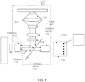
- FIG. 1 is a diagram illustrating an example embodiment of a flouresence imaging system 100 configured in accordance with the system and methods described herein.
- system 100 comprises a light source 104 configured to produce illumination light 104.
- the source 102 can for example be a Light Emitting Diode (LED) or a Laser, depending on the implementation.
- Pinhole optics 106 can then focus light 102 onto a pinhole mask 108.
- Light passing through mask 108 is then incident on mirror 110, such as a dichroic mirror, which directs the light onto sample 114, e.g., via objective optics 112.
- the light 104 is absorbed by fluorophores, which causes them to emit light 116, which passes back through objective 112 and mirror 110 an onto sensor 120.
- a filter 118 can filter the emissions prior the emissions being incident on sensor 120.
- system 100 can include a pinhole mask in the path of light emissions 116 as in conventional systems; however, as explained in detail below, the emissions path pinhole mask can be eliminated in other embodiments.
- the pinhole mask can comprise a predictable pattern that can be defined by a coordinate system, such as a rectangular, square or cylindrical coordinate system.
- a coordinate system such as a rectangular, square or cylindrical coordinate system.
- the mask can be moved in an x-y plane, e.g., as opposed to being rotated on a disk.
- Figure 5 is a diagram illustrating an example mask 500 in accordance with one embodiment.
- mask 500 can comprise multiple pinhole masks, such as masks 501 and 502.
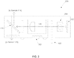
- the light source 102, imaging optics 106, mask 108, mirror 110 and filter 118 can be included in a very compact light cube 200.
- the light cube can also include a circuit board 220 that can be configured to communicate with a control system and to control various aspects of the light cube 200.
- the mask 500 of figure 5 can be configured to be inserted into light cube 200.
- images captured via conventional systems can include periodic visual artifacts, e.g., such as those caused by photobleaching. While conventional methods for reducing these artifacts can be helpful, system 100 can be configured to reduce the effect of such artifacts by capturing the individual partially illuminated images in a random order each time.
- FIG. 3 is a flow chart illustrating an example process for eliminating periodic artifacts such as those produced by photobleaching.
- an image control module 402 e.g., running on a control system 400 can determine the different physical locations that mask 106 must be located in order to properly construct a fully illuminated composite image. Normally, once these positions are determined, the system 400 would then control the translation stage via translation control module(s) 406 to move in a linear fashion, i.e., it would move through each position in order and capture the images. Control module 402 would normally also determine capture settings for each position and control the illumination control 408 in order to capture the images using the capture settings.
- control module 402 causes the translation stage to proceed to each one of the locations in a randomized order and capture the images in step 310. Further, the control module 402 can be configured to cause each image to be captured with the same capture settings each time. This allows for faster individual captures, since the camera or sensor and illumination control do not have to communicate with the control system 400 to confirm new settings before each capture.
- image processing module 404 can be used to generate the composite confocal image in step 315.
- the image processing module 404 can then be configured to differentiate signal from background information and measure the decrease in signal intensity at discrete steps in the capture process in step 320.
- a model such as a curve that has been modeled to match the experimentally observed behavior of photobleaching, i.e., relative brightness as a function of time, can then be fit to the data points in step 325. From that curve, the brightness of all images in the sequence, except the first, can be adjusted in step 330 to eliminate some of the apparent effect of the photobleaching.
- the composite image can be generated before or after the model is applied to the images and the brightness of various data points is adjusted.
- step 325) application of the model (step 325) can be applied to just a few images. Approximate correction of the brightness of the remaining images based on the application to a few images can then be performed as illustrated by optional step 335.
- the model can be applied to an image at the beginning, middle and end of the order and then an exponential decay can be fit to these points. This modified process can result in a relatively quick acquisition of a good quality image.
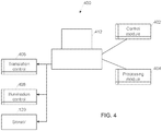
- FIG. 4 is a diagram illustrating an example control system 400 for controlling the operation of illumination system 100.
- system 400 comprises an image authority 412.
- Image authority 412 can comprise all of the resources need to implement certain portions of the system sand methods described herein.
- authority 412 can comprise all of the hardware and software resources needed for those portions including one or more processors, including any signal processors, math co-processors, microcontrollers, etc., one or more servers, one or more routers, one or more terminals, one or more computers, including desk top or portable computers, and all the API's, programs, software modules, etc., needed to perform the those portions or aspects of the systems and methods described herein.
- a module such as those described herein can comprise the hardware and software resources needed to perform the specified function.
- authority 412 can comprise various modules configured to control the operation of system 100 and to process data obtained therefrom. As illustrated in figure 4 , these modules can include an image control module 402, which can be configured to control the translation stages in system 100, e.g., via a translation control module 406. Control module 402 can also be configured to control the illumination via illumination control module 408.
- Authority 410 can also comprise a processing module 404 configured to process the image data obtained by sensor 120.
- translation control module 406 and illumination control module 408 can reside within system 100, e.g., within light cube 200 or within the translation stage to which cube 200 is interfaced.
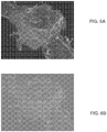
- Figures 6A and 6B illustrate an example wide-field image capture and a corresponding pin-hole image capture.
- a raster scanned confocal image can provide improved resolution and contrast; however, as illustrated in figures 6E and F , the randomly scanned image capture process of figure 3 can provide even better resolution and contrast in less time and with fewer processing resources.
- the systems described herein are multi-point confocal systems.
- a pattern of pinholes is printed on a small, e.g., glass slide as illustrated in figure 5 .
- This slide can be held in front of the excitation light source 102, e.g., as in the light cube configuration of figure 2 .
- the mask is moved around using small translation stages which position the mask in the appropriate location to illuminate a different part of the sample before each capture.
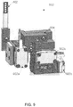
- Figure 9 is a diagram illustrating an example configuration of the translation apparatus 900, including a plurality of translation stages 902a, b, and c as well as tip/tilt adjustment mechanism 904 in accordance with one embodiment.
- the translation stages 902 and the tip/tilt adjustment mechanism 904 can move and position the mask 108, e.g., under the control of control module 402 and translation control 406.
- This type of translation apparatus 900 in addition to the light cube 200 provides a simple and compact solution that allows for several different pinhole patterns, e.g., 501 and 502, to be printed on each slide. This allows for more flexibility, giving the user a choice between speed and quality.
- the systems and methods described herein can be configured to eliminate the need for a pinhole mask on the emission path.
- the systems and methods described herein can be configured to use a high resolution sensor 120, such as a CCD or CMOS device, to virtually mask off the returned image, only recording data in the 'good' regions of the image.
- a high resolution sensor 120 such as a CCD or CMOS device
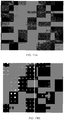
- the locations of the pinholes 108 relative to the sensor 120 must be known. This is accomplished by taking a calibration image at the beginning of the confocal capture routine and using image processing, e.g., within processing module 404 to determine the location of the pinhole array 108 relative to the sensor 120. In this way the system is at least partially self-calibrating and can tolerate small errors in image-to-image system positioning, such as the position of a light cube 200, without significant loss of image quality.
- the pinholes i.e., the bright spots in the image of figure 11A
- the data from these locations are processed to generate a confocal image, while data outside these regions is ignored.
- the process that can be used to establish the location of the pinhole array relative to the camera sensor has several discrete steps as illustrated in figure 10 .
- step 1010 various image processing techniques can be used to enhance the image of the mask to make it more suitable for quantitative analysis.
- a Fourier transform can be used to move the data into the frequency domain, in step 1015, where a bandpass filter can be used, in step 1020, to find data that corresponds with that spacing.
- Noise can then be removed and brightness variation across the image accounted for in step 1025.
- opening technique can be used in step 1025.
- the brightest data can then be selected in step 1030.
- a histogram binning technique can be used to keep only the brightest of this data.
- the pinholes in the enhanced image can be located in step 1035.
- a threshold algorithm can be applied that identifies regions of signal that are bright enough to be considered pinholes. The centroids of these regions can then be calculated and stored for use in the next step.
- the known mask pattern can be fit to the observed data, thereby relating the mask position to the sensor.
- a Random Sample Consensus (RANSAC) method can be used to apply and test a variety of rotation, scale and offset factors to the known mask pattern against two centroids at a time. This iterative process can be parallelized to allow the testing of hundreds of possibilities in seconds or less. Once the best fit is determined, the mask pattern is stored for use in the subsequent confocal capture routine.
- RANSAC Random Sample Consensus
- the entire process of figure 10 can be completed in a matter of seconds, while running on, e.g., a consumer grade computer it is possible and practical to run this calibration before each confocal capture. Further, since multiple pinholes are imaged at once, the system 100 can capture a high resolution image without the time penalty that would be incurred on a single-point system. Still further, compared to a spinning disk system the translating mask approach eliminates the problems of blurring and vibration since the pinholes are stationary during image captures.
- Figure 11A illustrated data captured for an image with the determined pinholes overlaid, wherein the pinhole locations where determined using the process of figure 10 .
- Figures 11B illustrates a close-up of the determined pinholes versus the raw data on the right.
- Figure 8 is a block diagram illustrating an example wired or wireless system 550 that can be used in connection with various embodiments described herein.
- the system 550 can be used as or in conjunction with one or more of the mechanisms or processes described above, and may represent components of system 100 or 400, the corresponding server(s), and/or other devices described herein.
- the system 550 can be a combination of one or more of the following: a server or any conventional personal computer, or any other processor-enabled device that is capable of wired or wireless data communication.
- Other computer systems and/or architectures may be also used, as will be clear to those skilled in the art.
- the system 550 preferably includes one or more processors, such as processor 560. Additional processors may be provided, such as an auxiliary processor to manage input/output, an auxiliary processor to perform floating point mathematical operations, a special-purpose microprocessor having an architecture suitable for fast execution of signal processing algorithms (e.g., digital signal processor), a slave processor subordinate to the main processing system (e.g., back-end processor), an additional microprocessor or controller for dual or multiple processor systems, or a coprocessor. Such auxiliary processors may be discrete processors or may be integrated with the processor 560. Examples of processors which may be used with system 550 include, without limitation, the Pentium® processor, Core i7® processor, and Xeon® processor, all of which are available from Intel Corporation of Santa Clara, California.
- the processor 560 is preferably connected to a communication bus 555.
- the communication bus 555 may include a data channel for facilitating information transfer between storage and other peripheral components of the system 550.
- the communication bus 555 further may provide a set of signals used for communication with the processor 560, including a data bus, address bus, and control bus (not shown).
- the communication bus 555 may comprise any standard or non-standard bus architecture such as, for example, bus architectures compliant with industry standard architecture (ISA), extended industry standard architecture (EISA), Micro Channel Architecture (MCA), peripheral component interconnect (PCI) local bus, or standards promulgated by the Institute of Electrical and Electronics Engineers (IEEE) including IEEE 488 general-purpose interface bus (GPIB), IEEE 696/S-100, and the like.
- ISA industry standard architecture
- EISA extended industry standard architecture
- MCA Micro Channel Architecture
- PCI peripheral component interconnect
- IEEE Institute of Electrical and Electronics Engineers
- IEEE Institute of Electrical and Electronics Engineers
- GPIB general-purpose interface
- System 550 preferably includes a main memory 565 and may also include a secondary memory 570.
- the main memory 565 provides storage of instructions and data for programs executing on the processor 560, such as one or more of the functions and/or modules discussed above. It should be understood that programs stored in the memory and executed by processor 560 may be written and/or compiled according to any suitable language, including without limitation C/C++, Java, JavaScript, Pearl, Visual Basic, .NET, and the like.
- the main memory 565 is typically semiconductor-based memory such as dynamic random access memory (DRAM) and/or static random access memory (SRAM). Other semiconductor-based memory types include, for example, synchronous dynamic random access memory (SDRAM), Rambus dynamic random access memory (RDRAM), ferroelectric random access memory (FRAM), and the like, including read only memory (ROM).
- SDRAM synchronous dynamic random access memory
- RDRAM Rambus dynamic random access memory
- FRAM ferroelectric random access memory
- ROM read only memory
- the secondary memory 570 may optionally include an internal memory 575 and/or a removable medium 580, for example a floppy disk drive, a magnetic tape drive, a compact disc (CD) drive, a digital versatile disc (DVD) drive, other optical drive, a flash memory drive, etc.
- the removable medium 580 is read from and/or written to in a well-known manner.
- Removable storage medium 580 may be, for example, a floppy disk, magnetic tape, CD, DVD, SD card, etc.
- the removable storage medium 580 is a non-transitory computer-readable medium having stored thereon computer executable code (i.e., software) and/or data.
- the computer software or data stored on the removable storage medium 580 is read into the system 550 for execution by the processor 560.
- secondary memory 570 may include other similar means for allowing computer programs or other data or instructions to be loaded into the system 550.
- Such means may include, for example, an external storage medium 595 and an interface 590.
- external storage medium 595 may include an external hard disk drive or an external optical drive, or and external magneto-optical drive.
- secondary memory 570 may include semiconductor-based memory such as programmable read-only memory (PROM), erasable programmable read-only memory (EPROM), electrically erasable read-only memory (EEPROM), or flash memory (block oriented memory similar to EEPROM). Also included are any other removable storage media 580 and communication interface 590, which allow software and data to be transferred from an external medium 595 to the system 550.
- PROM programmable read-only memory
- EPROM erasable programmable read-only memory
- EEPROM electrically erasable read-only memory
- flash memory block oriented memory similar to EEPROM
- System 550 may include a communication interface 590.
- the communication interface 590 allows software and data to be transferred between system 550 and external devices (e.g. printers), networks, or information sources.
- computer software or executable code may be transferred to system 550 from a network server via communication interface 590.
- Examples of communication interface 590 include a built-in network adapter, network interface card (NIC), Personal Computer Memory Card International Association (PCMCIA) network card, card bus network adapter, wireless network adapter, Universal Serial Bus (USB) network adapter, modem, a network interface card (NIC), a wireless data card, a communications port, an infrared interface, an IEEE 1394 fire-wire, or any other device capable of interfacing system 550 with a network or another computing device.
- NIC network interface card
- PCMCIA Personal Computer Memory Card International Association
- USB Universal Serial Bus
- Communication interface 590 preferably implements industry promulgated protocol standards, such as Ethernet IEEE 802 standards, Fiber Channel, digital subscriber line (DSL), asynchronous digital subscriber line (ADSL), frame relay, asynchronous transfer mode (ATM), integrated digital services network (ISDN), personal communications services (PCS), transmission control protocol/Internet protocol (TCP/IP), serial line Internet protocol/point to point protocol (SLIP/PPP), and so on, but may also implement customized or non-standard interface protocols as well.
- industry promulgated protocol standards such as Ethernet IEEE 802 standards, Fiber Channel, digital subscriber line (DSL), asynchronous digital subscriber line (ADSL), frame relay, asynchronous transfer mode (ATM), integrated digital services network (ISDN), personal communications services (PCS), transmission control protocol/Internet protocol (TCP/IP), serial line Internet protocol/point to point protocol (SLIP/PPP), and so on, but may also implement customized or non-standard interface protocols as well.
- industry promulgated protocol standards such as Ethernet IEEE 802 standards, Fiber Channel, digital subscriber
- Software and data transferred via communication interface 590 are generally in the form of electrical communication signals 605. These signals 605 are preferably provided to communication interface 590 via a communication channel 600.
- the communication channel 600 may be a wired or wireless network, or any variety of other communication links.
- Communication channel 600 carries signals 605 and can be implemented using a variety of wired or wireless communication means including wire or cable, fiber optics, conventional phone line, cellular phone link, wireless data communication link, radio frequency (“RF”) link, or infrared link, just to name a few.
- RF radio frequency
- Computer executable code i.e., computer programs or software
- main memory 565 and/or the secondary memory 570 Computer programs can also be received via communication interface 590 and stored in the main memory 565 and/or the secondary memory 570. Such computer programs, when executed, enable the system 550 to perform the various functions of the present invention as previously described.
- computer readable medium is used to refer to any non-transitory computer readable storage media used to provide computer executable code (e.g., software and computer programs) to the system 550.
- Examples of these media include main memory 565, secondary memory 570 (including internal memory 575, removable medium 580, and external storage medium 595), and any peripheral device communicatively coupled with communication interface 590 (including a network information server or other network device).
- These non-transitory computer readable mediums are means for providing executable code, programming instructions, and software to the system 550.
- the software may be stored on a computer readable medium and loaded into the system 550 by way of removable medium 580, I/O interface 585, or communication interface 590.
- the software is loaded into the system 550 in the form of electrical communication signals 605.
- the software when executed by the processor 560, preferably causes the processor 560 to perform the inventive features and functions previously described herein.
- I/O interface 585 provides an interface between one or more components of system 550 and one or more input and/or output devices.
- Example input devices include, without limitation, keyboards, touch screens or other touch-sensitive devices, biometric sensing devices, computer mice, trackballs, pen-based pointing devices, and the like.
- Examples of output devices include, without limitation, cathode ray tubes (CRTs), plasma displays, light-emitting diode (LED) displays, liquid crystal displays (LCDs), printers, vacuum florescent displays (VFDs), surface-conduction electron-emitter displays (SEDs), field emission displays (FEDs), and the like.
- CTRs cathode ray tubes
- LED light-emitting diode
- LCDs liquid crystal displays
- VFDs vacuum florescent displays
- SEDs surface-conduction electron-emitter displays
- FEDs field emission displays
- the system 550 also includes optional wireless communication components that facilitate wireless communication over a voice and over a data network.
- the wireless communication components comprise an antenna system 610, a radio system 615 and a baseband system 620.
- RF radio frequency
- the antenna system 610 may comprise one or more antennae and one or more multiplexors (not shown) that perform a switching function to provide the antenna system 610 with transmit and receive signal paths.
- received RF signals can be coupled from a multiplexor to a low noise amplifier (not shown) that amplifies the received RF signal and sends the amplified signal to the radio system 615.
- the radio system 615 may comprise one or more radios that are configured to communicate over various frequencies.
- the radio system 615 may combine a demodulator (not shown) and modulator (not shown) in one integrated circuit (IC).
- the demodulator and modulator can also be separate components. In the incoming path, the demodulator strips away the RF carrier signal leaving a baseband receive audio signal, which is sent from the radio system 615 to the baseband system 620.
- baseband system 620 decodes the signal and converts it to an analog signal. Then the signal is amplified and sent to a speaker.
- the baseband system 620 also receives analog audio signals from a microphone. These analog audio signals are converted to digital signals and encoded by the baseband system 620.
- the baseband system 620 also codes the digital signals for transmission and generates a baseband transmit audio signal that is routed to the modulator portion of the radio system 615.
- the modulator mixes the baseband transmit audio signal with an RF carrier signal generating an RF transmit signal that is routed to the antenna system and may pass through a power amplifier (not shown).
- the power amplifier amplifies the RF transmit signal and routes it to the antenna system 610 where the signal is switched to the antenna port for transmission.
- the baseband system 620 is also communicatively coupled with the processor 560.
- the central processing unit 560 has access to data storage areas 565 and 570.
- the central processing unit 560 is preferably configured to execute instructions (i.e., computer programs or software) that can be stored in the memory 565 or the secondary memory 570.
- Computer programs can also be received from the baseband processor 610 and stored in the data storage area 565 or in secondary memory 570, or executed upon receipt.
- Such computer programs when executed, enable the system 550 to perform the various functions of the present invention as previously described.
- data storage areas 565 may include various software modules (not shown).
- Various embodiments may also be implemented primarily in hardware using, for example, components such as application specific integrated circuits (ASICs), or field programmable gate arrays (FPGAs).
- ASICs application specific integrated circuits
- FPGAs field programmable gate arrays
- ASICs application specific integrated circuits
- FPGAs field programmable gate arrays
- DSP digital signal processor
- a general-purpose processor can be a microprocessor, but in the alternative, the processor can be any processor, controller, microcontroller, or state machine.
- a processor can also be implemented as a combination of computing devices, for example, a combination of a DSP and a microprocessor, a plurality of microprocessors, one or more microprocessors in conjunction with a DSP core, or any other such configuration.
- a software module can reside in RAM memory, flash memory, ROM memory, EPROM memory, EEPROM memory, registers, hard disk, a removable disk, a CD-ROM, or any other form of storage medium including a network storage medium.
- An exemplary storage medium can be coupled to the processor such that the processor can read information from, and write information to, the storage medium. In the alternative, the storage medium can be integral to the processor.
- the processor and the storage medium can also reside in an ASIC.
- a component may be a stand-alone software package, or it may be a software package incorporated as a "tool" in a larger software product. It may be downloadable from a network, for example, a website, as a stand-alone product or as an add-in package for installation in an existing software application. It may also be available as a client-server software application, as a web-enabled software application, and/or as a mobile application.
Claims (12)
- Système d'imagerie (100), comprenant :une source d'éclairage conçue pour éclairer un échantillon (114) à travers un masque sténopéique (108) à l'aide d'une lumière d'excitation (104) ;un appareil de translation (900) conçu pour déplacer le masque sténopéique (108) ou l'échantillon (114) vers un premier emplacement ;un capteur (120) conçu pour capturer une image de l'échantillon au premier emplacement et convertir l'image en données ;un module de traitement d'image (404) conçu pour :filtrer les données à l'aide de l'espacement connu des sténopés dans le masque sténopéique (108) pour obtenir des données correspondant à l'espacement, utiliser un seuil pour identifier les régions des données restantes suffisamment lumineuses pour être associées à un sténopé, calculer les centroïdes des régions, ajuster un motif connu au masque sténopéique (108) aux régions afin d'identifier le meilleur ajustement des données par rapport aux emplacements des sténopés ;un support de stockage conçu pour mémoriser les données de meilleur ajustement ; etun module de commande (402) conçu pour commander la source d'éclairage et l'appareil de translation (900) afin d'obtenir une pluralité d'images de l'échantillon destinées à être utilisées dans une routine de capture confocale ultérieure.
- Système selon la revendication 1, dans lequel le module de traitement d'image (404) est en outre conçu pour améliorer les données correspondant à l'image capturée.
- Système selon la revendication 2, dans lequel l'amélioration des données comprend l'amplification de la netteté et du contraste des données.
- Système selon la revendication 1, dans lequel le filtrage des données comprend la transformation des données du domaine fréquentiel et l'application d'un filtre passe-bande aux données transformées.
- Système selon la revendication 1, dans lequel le module de traitement d'image (404) est en outre conçu pour supprimer le bruit et tenir compte des variations de luminosité dans les données filtrées.
- Système selon la revendication 5, dans lequel le module de traitement d'image (404) est en outre conçu de manière à ne conserver que les données qui dépassent un seuil de luminosité.
- Système selon la revendication 6, dans lequel le module de traitement d'image (404) est en outre conçu pour appliquer une technique de regroupement d'histogramme pour identifier des données qui dépassent le seuil de luminosité.
- Système selon la revendication 1, dans lequel le module de traitement d'image (404) est en outre conçu pour appliquer au moins l'un parmi les facteurs de rotation, d'échelle et de décalage à des paires de centroïdes dans un processus itératif pour aider à identifier le meilleur ajustement.
- Système selon la revendication 1, dans lequel le module de traitement d'image (404) est en outre conçu pour utiliser les données de meilleur ajustement pour l'emplacement des sténopés afin d'obtenir une image composite confocale de l'échantillon, en traitant les données associées à l'emplacement des sténopés et en ignorant les données non associées à l'emplacement des sténopés.
- Système selon la revendication 1, dans lequel le capteur (120) comprend un dispositif à couplage de charge (CCD) ou un dispositif à CMOS.
- Système selon la revendication 1, dans lequel le module de traitement de formation d'image (404) est en outre conçu pour générer une image composite confocale en utilisant la pluralité d'images et les données de meilleur ajustement.
- Système selon la revendication 1, dans lequel le masque sténopéique (108) est un masque rectangulaire, carré ou cylindrique.
Priority Applications (1)
| Application Number | Priority Date | Filing Date | Title |
|---|---|---|---|
| EP19182013.3A EP3620838A1 (fr) | 2015-06-02 | 2016-05-10 | Systèmes et procédés permettant d'étalonner un système d'imagerie à éclairage structuré et permettant de capturer une image à éclairage structuré |
Applications Claiming Priority (2)
| Application Number | Priority Date | Filing Date | Title |
|---|---|---|---|
| US201562169675P | 2015-06-02 | 2015-06-02 | |
| PCT/US2016/031570 WO2016195927A1 (fr) | 2015-06-02 | 2016-05-10 | Systèmes et procédés permettant d'étalonner un système d'imagerie à éclairage structuré et permettant de capturer une image à éclairage structuré |
Related Child Applications (1)
| Application Number | Title | Priority Date | Filing Date |
|---|---|---|---|
| EP19182013.3A Division EP3620838A1 (fr) | 2015-06-02 | 2016-05-10 | Systèmes et procédés permettant d'étalonner un système d'imagerie à éclairage structuré et permettant de capturer une image à éclairage structuré |
Publications (2)
| Publication Number | Publication Date |
|---|---|
| EP3304166A1 EP3304166A1 (fr) | 2018-04-11 |
| EP3304166B1 true EP3304166B1 (fr) | 2019-06-26 |
Family
ID=56113047
Family Applications (2)
| Application Number | Title | Priority Date | Filing Date |
|---|---|---|---|
| EP16727874.6A Active EP3304166B1 (fr) | 2015-06-02 | 2016-05-10 | Systèmes et procédés permettant d'étalonner un système d'imagerie à éclairage structuré et permettant de capturer une image à éclairage structuré |
| EP19182013.3A Withdrawn EP3620838A1 (fr) | 2015-06-02 | 2016-05-10 | Systèmes et procédés permettant d'étalonner un système d'imagerie à éclairage structuré et permettant de capturer une image à éclairage structuré |
Family Applications After (1)
| Application Number | Title | Priority Date | Filing Date |
|---|---|---|---|
| EP19182013.3A Withdrawn EP3620838A1 (fr) | 2015-06-02 | 2016-05-10 | Systèmes et procédés permettant d'étalonner un système d'imagerie à éclairage structuré et permettant de capturer une image à éclairage structuré |
Country Status (5)
| Country | Link |
|---|---|
| US (1) | US10782514B2 (fr) |
| EP (2) | EP3304166B1 (fr) |
| JP (1) | JP7195738B2 (fr) |
| CN (1) | CN107667310B (fr) |
| WO (1) | WO2016195927A1 (fr) |
Families Citing this family (5)
| Publication number | Priority date | Publication date | Assignee | Title |
|---|---|---|---|---|
| JP6891130B2 (ja) * | 2015-06-02 | 2021-06-18 | ライフ テクノロジーズ コーポレーション | 構造化照明イメージを生成するためのシステムおよび方法 |
| WO2018140773A1 (fr) * | 2017-01-26 | 2018-08-02 | President And Fellows Of Harvard College | Sectionnement optique à grande vitesse et à large champ |
| CN108827920B (zh) * | 2018-03-21 | 2022-05-27 | 苏州国科医工科技发展(集团)有限公司 | 一种低荧光漂白共聚焦成像方法及系统 |
| EP3644044B1 (fr) * | 2018-10-24 | 2020-12-23 | Leica Biosystems Imaging, Inc. | Commande d'exposition de caméra lors de l'acquisition des images d'hybridation in situ en fluorescence |
| US11492140B2 (en) * | 2021-03-25 | 2022-11-08 | Rockwell Collins, Inc. | Camera monitor using close proximity precision injection of light |
Family Cites Families (42)
| Publication number | Priority date | Publication date | Assignee | Title |
|---|---|---|---|---|
| US3960449A (en) * | 1975-06-05 | 1976-06-01 | The Board Of Trustees Of Leland Stanford Junior University | Measurement of angular dependence of scattered light in a flowing stream |
| JPH01201135A (ja) * | 1988-02-04 | 1989-08-14 | Shimadzu Corp | 赤外線散乱トモグラフィ装置 |
| US5900949A (en) * | 1996-05-23 | 1999-05-04 | Hewlett-Packard Company | CCD imager for confocal scanning microscopy |
| JPH1183431A (ja) * | 1997-09-09 | 1999-03-26 | Nikon Corp | 撮像光学系の座標中心位置決定装置 |
| US6248988B1 (en) * | 1998-05-05 | 2001-06-19 | Kla-Tencor Corporation | Conventional and confocal multi-spot scanning optical microscope |
| US7147161B2 (en) * | 1998-06-12 | 2006-12-12 | Symbol Technologies, Inc. | Digitizing bar code symbol data |
| US6328213B1 (en) * | 1998-06-12 | 2001-12-11 | Symbol Technologies, Inc. | Method of processing an analog electrical signal containing information representative of reflected light from coded indicia, wherein the electrical signal contains edge transitions |
| DE29913707U1 (de) * | 1998-08-27 | 1999-11-25 | Evotec Biosystems Ag | Konfokale optische Vorrichtung zur optischen Erfassung eines Beobachtungsvolumens |
| US6307635B1 (en) * | 1998-10-21 | 2001-10-23 | The Regents Of The University Of California | Phase-shifting point diffraction interferometer mask designs |
| US7209287B2 (en) * | 2000-09-18 | 2007-04-24 | Vincent Lauer | Confocal optical scanning device |
| SG118191A1 (en) * | 2003-06-27 | 2006-01-27 | St Microelectronics Asia | Method and system for contrast enhancement of digital video |
| JP4756819B2 (ja) * | 2003-10-21 | 2011-08-24 | オリンパス株式会社 | 走査型顕微鏡システム |
| DE10350918B3 (de) * | 2003-10-31 | 2005-04-14 | Evotec Technologies Gmbh | Vorrichtung und Verfahren zur Messung der Transmission eines Objekts |
| DE502004002547D1 (de) * | 2004-06-22 | 2007-02-15 | Polytec Gmbh | Vorrichtung zum optischen Vermessen eines Objektes |
| US7115848B1 (en) * | 2004-09-29 | 2006-10-03 | Qioptiq Imaging Solutions, Inc. | Methods, systems and computer program products for calibration of microscopy imaging devices |
| WO2006058187A2 (fr) * | 2004-11-23 | 2006-06-01 | Robert Eric Betzig | Microscopie optique de reseau cristallin |
| DE102005020542A1 (de) | 2005-05-03 | 2006-11-09 | Carl Zeiss Jena Gmbh | Einrichtung und Verfahren zur reproduzierbaren Einstellung der Pinholeöffnung und Pinholelage in Laserscanmikroskopen |
| DE102006007170B4 (de) | 2006-02-08 | 2009-06-10 | Sirona Dental Systems Gmbh | Verfahren und Anordnung zur schnellen und robusten chromatisch konfokalen 3D-Messtechnik |
| US7460248B2 (en) * | 2006-05-15 | 2008-12-02 | Carestream Health, Inc. | Tissue imaging system |
| JP4288519B2 (ja) * | 2006-09-13 | 2009-07-01 | セイコーエプソン株式会社 | アライメント装置及びアライメント方法 |
| TWI422962B (zh) * | 2006-12-05 | 2014-01-11 | Hoya Corp | 灰階光罩之檢查方法、液晶裝置製造用灰階光罩之製造方法以及圖案轉印方法 |
| CN101543054B (zh) * | 2007-06-28 | 2011-12-07 | 松下电器产业株式会社 | 图像处理装置、图像处理方法 |
| FI20085062A0 (fi) * | 2008-01-25 | 2008-01-25 | Wallac Oy | Parannettu mittausjärjestelmä ja -menetelmä |
| EP2211343A1 (fr) * | 2009-01-27 | 2010-07-28 | Thomson Licensing | Support d'enregistrement optique à haute densité de données |
| US8218869B2 (en) * | 2009-03-29 | 2012-07-10 | Mitsubishi Electric Research Laboratories, Inc. | Image segmentation using spatial random walks |
| JP5544764B2 (ja) * | 2009-06-09 | 2014-07-09 | ソニー株式会社 | 画像処理装置および方法、並びにプログラム |
| CN101710131B (zh) * | 2009-12-01 | 2011-06-01 | 西安交通大学 | 离焦数字三维微流场荧光测试仪 |
| WO2012039352A1 (fr) * | 2010-09-21 | 2012-03-29 | オリンパス株式会社 | Méthode d'analyse photométrique par détection de particules luminescentes uniques |
| US8559008B2 (en) | 2011-04-07 | 2013-10-15 | Nanometrics Incorporated | Ellipsometer focusing system |
| DE102011114500B4 (de) * | 2011-09-29 | 2022-05-05 | Fei Company | Mikroskopvorrichtung |
| US8908913B2 (en) * | 2011-12-19 | 2014-12-09 | Mitsubishi Electric Research Laboratories, Inc. | Voting-based pose estimation for 3D sensors |
| WO2013126762A1 (fr) * | 2012-02-23 | 2013-08-29 | The United States Of America, As Represented By The Secretary, Department Of Health And Human Services Office Of Technology Transfer, National Institutes Of Health | Systèmes et procédés de microscopie à éclairage structuré à foyers multiples |
| EP2966492B1 (fr) * | 2012-05-02 | 2020-10-21 | Centre National De La Recherche Scientifique | Procédé et appareil de localisation de particules uniques au moyen d'une analyse d'ondelettes |
| DE102012009836A1 (de) | 2012-05-16 | 2013-11-21 | Carl Zeiss Microscopy Gmbh | Lichtmikroskop und Verfahren zur Bildaufnahme mit einem Lichtmikroskop |
| US9183631B2 (en) * | 2012-06-29 | 2015-11-10 | Mitsubishi Electric Research Laboratories, Inc. | Method for registering points and planes of 3D data in multiple coordinate systems |
| US10073045B2 (en) * | 2012-07-24 | 2018-09-11 | Nova Measuring Instruments Ltd. | Optical method and system for measuring isolated features of a structure |
| DE102012217967A1 (de) * | 2012-10-01 | 2014-04-03 | Carl Zeiss Microscopy Gmbh | Konfokales Mikroskop mit frei einstellbarer Probenabtastung |
| US9830865B2 (en) * | 2013-04-04 | 2017-11-28 | Nvidia Corporation | Regional histogramming for global approximation |
| KR101716928B1 (ko) * | 2013-08-22 | 2017-03-15 | 주식회사 만도 | 차량 카메라의 영상 처리 방법 및 이를 이용하는 영상 처리 장치 |
| GB201318598D0 (en) * | 2013-10-21 | 2013-12-04 | Univ Leicester | Improvements in or relating to super-resolution microscopy |
| JP2015084062A (ja) * | 2013-10-25 | 2015-04-30 | 株式会社キーエンス | 顕微鏡撮像装置、顕微鏡撮像方法および顕微鏡撮像プログラム |
| CN104597590B (zh) * | 2014-12-30 | 2018-02-02 | 深圳先进技术研究院 | 一种超分辨荧光光谱成像显微镜 |
-
2016
- 2016-05-10 CN CN201680032373.4A patent/CN107667310B/zh active Active
- 2016-05-10 EP EP16727874.6A patent/EP3304166B1/fr active Active
- 2016-05-10 JP JP2017562599A patent/JP7195738B2/ja active Active
- 2016-05-10 WO PCT/US2016/031570 patent/WO2016195927A1/fr active Application Filing
- 2016-05-10 EP EP19182013.3A patent/EP3620838A1/fr not_active Withdrawn
-
2017
- 2017-11-29 US US15/826,125 patent/US10782514B2/en active Active
Non-Patent Citations (1)
| Title |
|---|
| None * |
Also Published As
| Publication number | Publication date |
|---|---|
| US20180157022A1 (en) | 2018-06-07 |
| US10782514B2 (en) | 2020-09-22 |
| CN107667310A (zh) | 2018-02-06 |
| EP3304166A1 (fr) | 2018-04-11 |
| JP7195738B2 (ja) | 2022-12-26 |
| WO2016195927A1 (fr) | 2016-12-08 |
| EP3620838A1 (fr) | 2020-03-11 |
| JP2018523154A (ja) | 2018-08-16 |
| CN107667310B (zh) | 2021-01-01 |
Similar Documents
| Publication | Publication Date | Title |
|---|---|---|
| US10782514B2 (en) | Systems and methods for calibrating a structured illumination imaging system and for capturing a structured illumination image | |
| JP6416887B2 (ja) | 構造化照明を用いた組織試料の顕微鏡観察 | |
| US10580128B2 (en) | Whole slide multispectral imaging systems and methods | |
| JP4826586B2 (ja) | スペクトル画像処理方法、コンピュータ実行可能なスペクトル画像処理プログラム、スペクトルイメージングシステム | |
| US10684461B2 (en) | Digital pathology system | |
| US11215806B2 (en) | Method for imaging a sample by means of a microscope and microscope | |
| US20200265570A1 (en) | Reducing image artifacts in images | |
| WO2017217325A1 (fr) | Dispositif de récupération de données, système de microscope et procédé de récupération de données | |
| US10921574B2 (en) | Systems and methods for stabilizing a sample stage in a structured illumination imaging system | |
| US11215803B2 (en) | Systems and methods for an interchangeable illumination filter set for use in a structured illumination imaging system | |
| US10634892B2 (en) | Systems and methods for generating a structured illumination image |
Legal Events
| Date | Code | Title | Description |
|---|---|---|---|
| STAA | Information on the status of an ep patent application or granted ep patent |
Free format text: STATUS: THE INTERNATIONAL PUBLICATION HAS BEEN MADE |
|
| PUAI | Public reference made under article 153(3) epc to a published international application that has entered the european phase |
Free format text: ORIGINAL CODE: 0009012 |
|
| STAA | Information on the status of an ep patent application or granted ep patent |
Free format text: STATUS: REQUEST FOR EXAMINATION WAS MADE |
|
| 17P | Request for examination filed |
Effective date: 20171204 |
|
| AK | Designated contracting states |
Kind code of ref document: A1 Designated state(s): AL AT BE BG CH CY CZ DE DK EE ES FI FR GB GR HR HU IE IS IT LI LT LU LV MC MK MT NL NO PL PT RO RS SE SI SK SM TR |
|
| AX | Request for extension of the european patent |
Extension state: BA ME |
|
| DAV | Request for validation of the european patent (deleted) | ||
| DAX | Request for extension of the european patent (deleted) | ||
| GRAP | Despatch of communication of intention to grant a patent |
Free format text: ORIGINAL CODE: EPIDOSNIGR1 |
|
| STAA | Information on the status of an ep patent application or granted ep patent |
Free format text: STATUS: GRANT OF PATENT IS INTENDED |
|
| INTG | Intention to grant announced |
Effective date: 20181219 |
|
| GRAS | Grant fee paid |
Free format text: ORIGINAL CODE: EPIDOSNIGR3 |
|
| GRAA | (expected) grant |
Free format text: ORIGINAL CODE: 0009210 |
|
| STAA | Information on the status of an ep patent application or granted ep patent |
Free format text: STATUS: THE PATENT HAS BEEN GRANTED |
|
| AK | Designated contracting states |
Kind code of ref document: B1 Designated state(s): AL AT BE BG CH CY CZ DE DK EE ES FI FR GB GR HR HU IE IS IT LI LT LU LV MC MK MT NL NO PL PT RO RS SE SI SK SM TR |
|
| REG | Reference to a national code |
Ref country code: GB Ref legal event code: FG4D |
|
| REG | Reference to a national code |
Ref country code: CH Ref legal event code: EP |
|
| REG | Reference to a national code |
Ref country code: AT Ref legal event code: REF Ref document number: 1148961 Country of ref document: AT Kind code of ref document: T Effective date: 20190715 |
|
| REG | Reference to a national code |
Ref country code: DE Ref legal event code: R096 Ref document number: 602016015946 Country of ref document: DE |
|
| REG | Reference to a national code |
Ref country code: IE Ref legal event code: FG4D |
|
| REG | Reference to a national code |
Ref country code: NL Ref legal event code: MP Effective date: 20190626 |
|
| PG25 | Lapsed in a contracting state [announced via postgrant information from national office to epo] |
Ref country code: SE Free format text: LAPSE BECAUSE OF FAILURE TO SUBMIT A TRANSLATION OF THE DESCRIPTION OR TO PAY THE FEE WITHIN THE PRESCRIBED TIME-LIMIT Effective date: 20190626 Ref country code: LT Free format text: LAPSE BECAUSE OF FAILURE TO SUBMIT A TRANSLATION OF THE DESCRIPTION OR TO PAY THE FEE WITHIN THE PRESCRIBED TIME-LIMIT Effective date: 20190626 Ref country code: FI Free format text: LAPSE BECAUSE OF FAILURE TO SUBMIT A TRANSLATION OF THE DESCRIPTION OR TO PAY THE FEE WITHIN THE PRESCRIBED TIME-LIMIT Effective date: 20190626 Ref country code: AL Free format text: LAPSE BECAUSE OF FAILURE TO SUBMIT A TRANSLATION OF THE DESCRIPTION OR TO PAY THE FEE WITHIN THE PRESCRIBED TIME-LIMIT Effective date: 20190626 Ref country code: HR Free format text: LAPSE BECAUSE OF FAILURE TO SUBMIT A TRANSLATION OF THE DESCRIPTION OR TO PAY THE FEE WITHIN THE PRESCRIBED TIME-LIMIT Effective date: 20190626 Ref country code: NO Free format text: LAPSE BECAUSE OF FAILURE TO SUBMIT A TRANSLATION OF THE DESCRIPTION OR TO PAY THE FEE WITHIN THE PRESCRIBED TIME-LIMIT Effective date: 20190926 |
|
| REG | Reference to a national code |
Ref country code: LT Ref legal event code: MG4D |
|
| PG25 | Lapsed in a contracting state [announced via postgrant information from national office to epo] |
Ref country code: GR Free format text: LAPSE BECAUSE OF FAILURE TO SUBMIT A TRANSLATION OF THE DESCRIPTION OR TO PAY THE FEE WITHIN THE PRESCRIBED TIME-LIMIT Effective date: 20190927 Ref country code: LV Free format text: LAPSE BECAUSE OF FAILURE TO SUBMIT A TRANSLATION OF THE DESCRIPTION OR TO PAY THE FEE WITHIN THE PRESCRIBED TIME-LIMIT Effective date: 20190626 Ref country code: BG Free format text: LAPSE BECAUSE OF FAILURE TO SUBMIT A TRANSLATION OF THE DESCRIPTION OR TO PAY THE FEE WITHIN THE PRESCRIBED TIME-LIMIT Effective date: 20190926 Ref country code: RS Free format text: LAPSE BECAUSE OF FAILURE TO SUBMIT A TRANSLATION OF THE DESCRIPTION OR TO PAY THE FEE WITHIN THE PRESCRIBED TIME-LIMIT Effective date: 20190626 |
|
| REG | Reference to a national code |
Ref country code: AT Ref legal event code: MK05 Ref document number: 1148961 Country of ref document: AT Kind code of ref document: T Effective date: 20190626 |
|
| PG25 | Lapsed in a contracting state [announced via postgrant information from national office to epo] |
Ref country code: NL Free format text: LAPSE BECAUSE OF FAILURE TO SUBMIT A TRANSLATION OF THE DESCRIPTION OR TO PAY THE FEE WITHIN THE PRESCRIBED TIME-LIMIT Effective date: 20190626 Ref country code: AT Free format text: LAPSE BECAUSE OF FAILURE TO SUBMIT A TRANSLATION OF THE DESCRIPTION OR TO PAY THE FEE WITHIN THE PRESCRIBED TIME-LIMIT Effective date: 20190626 Ref country code: EE Free format text: LAPSE BECAUSE OF FAILURE TO SUBMIT A TRANSLATION OF THE DESCRIPTION OR TO PAY THE FEE WITHIN THE PRESCRIBED TIME-LIMIT Effective date: 20190626 Ref country code: PT Free format text: LAPSE BECAUSE OF FAILURE TO SUBMIT A TRANSLATION OF THE DESCRIPTION OR TO PAY THE FEE WITHIN THE PRESCRIBED TIME-LIMIT Effective date: 20191028 Ref country code: RO Free format text: LAPSE BECAUSE OF FAILURE TO SUBMIT A TRANSLATION OF THE DESCRIPTION OR TO PAY THE FEE WITHIN THE PRESCRIBED TIME-LIMIT Effective date: 20190626 Ref country code: CZ Free format text: LAPSE BECAUSE OF FAILURE TO SUBMIT A TRANSLATION OF THE DESCRIPTION OR TO PAY THE FEE WITHIN THE PRESCRIBED TIME-LIMIT Effective date: 20190626 Ref country code: SK Free format text: LAPSE BECAUSE OF FAILURE TO SUBMIT A TRANSLATION OF THE DESCRIPTION OR TO PAY THE FEE WITHIN THE PRESCRIBED TIME-LIMIT Effective date: 20190626 |
|
| PG25 | Lapsed in a contracting state [announced via postgrant information from national office to epo] |
Ref country code: ES Free format text: LAPSE BECAUSE OF FAILURE TO SUBMIT A TRANSLATION OF THE DESCRIPTION OR TO PAY THE FEE WITHIN THE PRESCRIBED TIME-LIMIT Effective date: 20190626 Ref country code: SM Free format text: LAPSE BECAUSE OF FAILURE TO SUBMIT A TRANSLATION OF THE DESCRIPTION OR TO PAY THE FEE WITHIN THE PRESCRIBED TIME-LIMIT Effective date: 20190626 Ref country code: IS Free format text: LAPSE BECAUSE OF FAILURE TO SUBMIT A TRANSLATION OF THE DESCRIPTION OR TO PAY THE FEE WITHIN THE PRESCRIBED TIME-LIMIT Effective date: 20191026 Ref country code: IT Free format text: LAPSE BECAUSE OF FAILURE TO SUBMIT A TRANSLATION OF THE DESCRIPTION OR TO PAY THE FEE WITHIN THE PRESCRIBED TIME-LIMIT Effective date: 20190626 |
|
| PG25 | Lapsed in a contracting state [announced via postgrant information from national office to epo] |
Ref country code: TR Free format text: LAPSE BECAUSE OF FAILURE TO SUBMIT A TRANSLATION OF THE DESCRIPTION OR TO PAY THE FEE WITHIN THE PRESCRIBED TIME-LIMIT Effective date: 20190626 |
|
| PG25 | Lapsed in a contracting state [announced via postgrant information from national office to epo] |
Ref country code: DK Free format text: LAPSE BECAUSE OF FAILURE TO SUBMIT A TRANSLATION OF THE DESCRIPTION OR TO PAY THE FEE WITHIN THE PRESCRIBED TIME-LIMIT Effective date: 20190626 Ref country code: PL Free format text: LAPSE BECAUSE OF FAILURE TO SUBMIT A TRANSLATION OF THE DESCRIPTION OR TO PAY THE FEE WITHIN THE PRESCRIBED TIME-LIMIT Effective date: 20190626 |
|
| PG25 | Lapsed in a contracting state [announced via postgrant information from national office to epo] |
Ref country code: IS Free format text: LAPSE BECAUSE OF FAILURE TO SUBMIT A TRANSLATION OF THE DESCRIPTION OR TO PAY THE FEE WITHIN THE PRESCRIBED TIME-LIMIT Effective date: 20200224 |
|
| REG | Reference to a national code |
Ref country code: DE Ref legal event code: R097 Ref document number: 602016015946 Country of ref document: DE |
|
| PLBE | No opposition filed within time limit |
Free format text: ORIGINAL CODE: 0009261 |
|
| STAA | Information on the status of an ep patent application or granted ep patent |
Free format text: STATUS: NO OPPOSITION FILED WITHIN TIME LIMIT |
|
| PG2D | Information on lapse in contracting state deleted |
Ref country code: IS |
|
| 26N | No opposition filed |
Effective date: 20200603 |
|
| PG25 | Lapsed in a contracting state [announced via postgrant information from national office to epo] |
Ref country code: SI Free format text: LAPSE BECAUSE OF FAILURE TO SUBMIT A TRANSLATION OF THE DESCRIPTION OR TO PAY THE FEE WITHIN THE PRESCRIBED TIME-LIMIT Effective date: 20190626 |
|
| PG25 | Lapsed in a contracting state [announced via postgrant information from national office to epo] |
Ref country code: CH Free format text: LAPSE BECAUSE OF NON-PAYMENT OF DUE FEES Effective date: 20200531 Ref country code: MC Free format text: LAPSE BECAUSE OF FAILURE TO SUBMIT A TRANSLATION OF THE DESCRIPTION OR TO PAY THE FEE WITHIN THE PRESCRIBED TIME-LIMIT Effective date: 20190626 Ref country code: LI Free format text: LAPSE BECAUSE OF NON-PAYMENT OF DUE FEES Effective date: 20200531 |
|
| REG | Reference to a national code |
Ref country code: BE Ref legal event code: MM Effective date: 20200531 |
|
| PG25 | Lapsed in a contracting state [announced via postgrant information from national office to epo] |
Ref country code: LU Free format text: LAPSE BECAUSE OF NON-PAYMENT OF DUE FEES Effective date: 20200510 |
|
| PG25 | Lapsed in a contracting state [announced via postgrant information from national office to epo] |
Ref country code: IE Free format text: LAPSE BECAUSE OF NON-PAYMENT OF DUE FEES Effective date: 20200510 |
|
| PG25 | Lapsed in a contracting state [announced via postgrant information from national office to epo] |
Ref country code: BE Free format text: LAPSE BECAUSE OF NON-PAYMENT OF DUE FEES Effective date: 20200531 |
|
| PG25 | Lapsed in a contracting state [announced via postgrant information from national office to epo] |
Ref country code: MT Free format text: LAPSE BECAUSE OF FAILURE TO SUBMIT A TRANSLATION OF THE DESCRIPTION OR TO PAY THE FEE WITHIN THE PRESCRIBED TIME-LIMIT Effective date: 20190626 Ref country code: CY Free format text: LAPSE BECAUSE OF FAILURE TO SUBMIT A TRANSLATION OF THE DESCRIPTION OR TO PAY THE FEE WITHIN THE PRESCRIBED TIME-LIMIT Effective date: 20190626 |
|
| PG25 | Lapsed in a contracting state [announced via postgrant information from national office to epo] |
Ref country code: MK Free format text: LAPSE BECAUSE OF FAILURE TO SUBMIT A TRANSLATION OF THE DESCRIPTION OR TO PAY THE FEE WITHIN THE PRESCRIBED TIME-LIMIT Effective date: 20190626 |
|
| PGFP | Annual fee paid to national office [announced via postgrant information from national office to epo] |
Ref country code: FR Payment date: 20230529 Year of fee payment: 8 Ref country code: DE Payment date: 20230515 Year of fee payment: 8 |
|
| PGFP | Annual fee paid to national office [announced via postgrant information from national office to epo] |
Ref country code: GB Payment date: 20230518 Year of fee payment: 8 |