EP3300118A1 - Flexible display - Google Patents
Flexible display Download PDFInfo
- Publication number
- EP3300118A1 EP3300118A1 EP17191834.5A EP17191834A EP3300118A1 EP 3300118 A1 EP3300118 A1 EP 3300118A1 EP 17191834 A EP17191834 A EP 17191834A EP 3300118 A1 EP3300118 A1 EP 3300118A1
- Authority
- EP
- European Patent Office
- Prior art keywords
- layer
- lower layer
- flexible display
- sinx
- plastic substrate
- Prior art date
- Legal status (The legal status is an assumption and is not a legal conclusion. Google has not performed a legal analysis and makes no representation as to the accuracy of the status listed.)
- Granted
Links
Images



Classifications
-
- H—ELECTRICITY
- H10—SEMICONDUCTOR DEVICES; ELECTRIC SOLID-STATE DEVICES NOT OTHERWISE PROVIDED FOR
- H10K—ORGANIC ELECTRIC SOLID-STATE DEVICES
- H10K77/00—Constructional details of devices covered by this subclass and not covered by groups H10K10/80, H10K30/80, H10K50/80 or H10K59/80
- H10K77/10—Substrates, e.g. flexible substrates
- H10K77/111—Flexible substrates
-
- G—PHYSICS
- G09—EDUCATION; CRYPTOGRAPHY; DISPLAY; ADVERTISING; SEALS
- G09F—DISPLAYING; ADVERTISING; SIGNS; LABELS OR NAME-PLATES; SEALS
- G09F9/00—Indicating arrangements for variable information in which the information is built-up on a support by selection or combination of individual elements
- G09F9/30—Indicating arrangements for variable information in which the information is built-up on a support by selection or combination of individual elements in which the desired character or characters are formed by combining individual elements
- G09F9/301—Indicating arrangements for variable information in which the information is built-up on a support by selection or combination of individual elements in which the desired character or characters are formed by combining individual elements flexible foldable or roll-able electronic displays, e.g. thin LCD, OLED
-
- H—ELECTRICITY
- H10—SEMICONDUCTOR DEVICES; ELECTRIC SOLID-STATE DEVICES NOT OTHERWISE PROVIDED FOR
- H10D—INORGANIC ELECTRIC SEMICONDUCTOR DEVICES
- H10D30/00—Field-effect transistors [FET]
- H10D30/60—Insulated-gate field-effect transistors [IGFET]
- H10D30/67—Thin-film transistors [TFT]
- H10D30/6704—Thin-film transistors [TFT] having supplementary regions or layers in the thin films or in the insulated bulk substrates for controlling properties of the device
- H10D30/6713—Thin-film transistors [TFT] having supplementary regions or layers in the thin films or in the insulated bulk substrates for controlling properties of the device characterised by the properties of the source or drain regions, e.g. compositions or sectional shapes
-
- H—ELECTRICITY
- H10—SEMICONDUCTOR DEVICES; ELECTRIC SOLID-STATE DEVICES NOT OTHERWISE PROVIDED FOR
- H10D—INORGANIC ELECTRIC SEMICONDUCTOR DEVICES
- H10D30/00—Field-effect transistors [FET]
- H10D30/60—Insulated-gate field-effect transistors [IGFET]
- H10D30/67—Thin-film transistors [TFT]
- H10D30/6704—Thin-film transistors [TFT] having supplementary regions or layers in the thin films or in the insulated bulk substrates for controlling properties of the device
- H10D30/6723—Thin-film transistors [TFT] having supplementary regions or layers in the thin films or in the insulated bulk substrates for controlling properties of the device having light shields
-
- H—ELECTRICITY
- H10—SEMICONDUCTOR DEVICES; ELECTRIC SOLID-STATE DEVICES NOT OTHERWISE PROVIDED FOR
- H10D—INORGANIC ELECTRIC SEMICONDUCTOR DEVICES
- H10D30/00—Field-effect transistors [FET]
- H10D30/60—Insulated-gate field-effect transistors [IGFET]
- H10D30/67—Thin-film transistors [TFT]
- H10D30/6729—Thin-film transistors [TFT] characterised by the electrodes
-
- H—ELECTRICITY
- H10—SEMICONDUCTOR DEVICES; ELECTRIC SOLID-STATE DEVICES NOT OTHERWISE PROVIDED FOR
- H10D—INORGANIC ELECTRIC SEMICONDUCTOR DEVICES
- H10D30/00—Field-effect transistors [FET]
- H10D30/60—Insulated-gate field-effect transistors [IGFET]
- H10D30/67—Thin-film transistors [TFT]
- H10D30/674—Thin-film transistors [TFT] characterised by the active materials
- H10D30/6755—Oxide semiconductors, e.g. zinc oxide, copper aluminium oxide or cadmium stannate
-
- H—ELECTRICITY
- H10—SEMICONDUCTOR DEVICES; ELECTRIC SOLID-STATE DEVICES NOT OTHERWISE PROVIDED FOR
- H10D—INORGANIC ELECTRIC SEMICONDUCTOR DEVICES
- H10D30/00—Field-effect transistors [FET]
- H10D30/60—Insulated-gate field-effect transistors [IGFET]
- H10D30/67—Thin-film transistors [TFT]
- H10D30/6758—Thin-film transistors [TFT] characterised by the insulating substrates
-
- H—ELECTRICITY
- H10—SEMICONDUCTOR DEVICES; ELECTRIC SOLID-STATE DEVICES NOT OTHERWISE PROVIDED FOR
- H10D—INORGANIC ELECTRIC SEMICONDUCTOR DEVICES
- H10D86/00—Integrated devices formed in or on insulating or conducting substrates, e.g. formed in silicon-on-insulator [SOI] substrates or on stainless steel or glass substrates
- H10D86/40—Integrated devices formed in or on insulating or conducting substrates, e.g. formed in silicon-on-insulator [SOI] substrates or on stainless steel or glass substrates characterised by multiple TFTs
- H10D86/411—Integrated devices formed in or on insulating or conducting substrates, e.g. formed in silicon-on-insulator [SOI] substrates or on stainless steel or glass substrates characterised by multiple TFTs characterised by materials, geometry or structure of the substrates
-
- H—ELECTRICITY
- H10—SEMICONDUCTOR DEVICES; ELECTRIC SOLID-STATE DEVICES NOT OTHERWISE PROVIDED FOR
- H10D—INORGANIC ELECTRIC SEMICONDUCTOR DEVICES
- H10D86/00—Integrated devices formed in or on insulating or conducting substrates, e.g. formed in silicon-on-insulator [SOI] substrates or on stainless steel or glass substrates
- H10D86/40—Integrated devices formed in or on insulating or conducting substrates, e.g. formed in silicon-on-insulator [SOI] substrates or on stainless steel or glass substrates characterised by multiple TFTs
- H10D86/421—Integrated devices formed in or on insulating or conducting substrates, e.g. formed in silicon-on-insulator [SOI] substrates or on stainless steel or glass substrates characterised by multiple TFTs having a particular composition, shape or crystalline structure of the active layer
- H10D86/423—Integrated devices formed in or on insulating or conducting substrates, e.g. formed in silicon-on-insulator [SOI] substrates or on stainless steel or glass substrates characterised by multiple TFTs having a particular composition, shape or crystalline structure of the active layer comprising semiconductor materials not belonging to the Group IV, e.g. InGaZnO
-
- H—ELECTRICITY
- H10—SEMICONDUCTOR DEVICES; ELECTRIC SOLID-STATE DEVICES NOT OTHERWISE PROVIDED FOR
- H10D—INORGANIC ELECTRIC SEMICONDUCTOR DEVICES
- H10D86/00—Integrated devices formed in or on insulating or conducting substrates, e.g. formed in silicon-on-insulator [SOI] substrates or on stainless steel or glass substrates
- H10D86/40—Integrated devices formed in or on insulating or conducting substrates, e.g. formed in silicon-on-insulator [SOI] substrates or on stainless steel or glass substrates characterised by multiple TFTs
- H10D86/60—Integrated devices formed in or on insulating or conducting substrates, e.g. formed in silicon-on-insulator [SOI] substrates or on stainless steel or glass substrates characterised by multiple TFTs wherein the TFTs are in active matrices
-
- H—ELECTRICITY
- H10—SEMICONDUCTOR DEVICES; ELECTRIC SOLID-STATE DEVICES NOT OTHERWISE PROVIDED FOR
- H10K—ORGANIC ELECTRIC SOLID-STATE DEVICES
- H10K59/00—Integrated devices, or assemblies of multiple devices, comprising at least one organic light-emitting element covered by group H10K50/00
- H10K59/10—OLED displays
- H10K59/12—Active-matrix OLED [AMOLED] displays
-
- H—ELECTRICITY
- H10—SEMICONDUCTOR DEVICES; ELECTRIC SOLID-STATE DEVICES NOT OTHERWISE PROVIDED FOR
- H10P—GENERIC PROCESSES OR APPARATUS FOR THE MANUFACTURE OR TREATMENT OF DEVICES COVERED BY CLASS H10
- H10P14/00—Formation of materials, e.g. in the shape of layers or pillars
- H10P14/20—Formation of materials, e.g. in the shape of layers or pillars of semiconductor materials
-
- H—ELECTRICITY
- H10—SEMICONDUCTOR DEVICES; ELECTRIC SOLID-STATE DEVICES NOT OTHERWISE PROVIDED FOR
- H10P—GENERIC PROCESSES OR APPARATUS FOR THE MANUFACTURE OR TREATMENT OF DEVICES COVERED BY CLASS H10
- H10P14/00—Formation of materials, e.g. in the shape of layers or pillars
- H10P14/20—Formation of materials, e.g. in the shape of layers or pillars of semiconductor materials
- H10P14/34—Deposited materials, e.g. layers
- H10P14/3402—Deposited materials, e.g. layers characterised by the chemical composition
-
- H—ELECTRICITY
- H10—SEMICONDUCTOR DEVICES; ELECTRIC SOLID-STATE DEVICES NOT OTHERWISE PROVIDED FOR
- H10P—GENERIC PROCESSES OR APPARATUS FOR THE MANUFACTURE OR TREATMENT OF DEVICES COVERED BY CLASS H10
- H10P14/00—Formation of materials, e.g. in the shape of layers or pillars
- H10P14/40—Formation of materials, e.g. in the shape of layers or pillars of conductive or resistive materials
-
- H—ELECTRICITY
- H10—SEMICONDUCTOR DEVICES; ELECTRIC SOLID-STATE DEVICES NOT OTHERWISE PROVIDED FOR
- H10P—GENERIC PROCESSES OR APPARATUS FOR THE MANUFACTURE OR TREATMENT OF DEVICES COVERED BY CLASS H10
- H10P14/00—Formation of materials, e.g. in the shape of layers or pillars
- H10P14/60—Formation of materials, e.g. in the shape of layers or pillars of insulating materials
- H10P14/69—Inorganic materials
- H10P14/692—Inorganic materials composed of oxides, glassy oxides or oxide-based glasses
- H10P14/6921—Inorganic materials composed of oxides, glassy oxides or oxide-based glasses containing silicon
- H10P14/69215—Inorganic materials composed of oxides, glassy oxides or oxide-based glasses containing silicon the material being a silicon oxide, e.g. SiO2
-
- H—ELECTRICITY
- H10—SEMICONDUCTOR DEVICES; ELECTRIC SOLID-STATE DEVICES NOT OTHERWISE PROVIDED FOR
- H10P—GENERIC PROCESSES OR APPARATUS FOR THE MANUFACTURE OR TREATMENT OF DEVICES COVERED BY CLASS H10
- H10P14/00—Formation of materials, e.g. in the shape of layers or pillars
- H10P14/60—Formation of materials, e.g. in the shape of layers or pillars of insulating materials
- H10P14/69—Inorganic materials
- H10P14/692—Inorganic materials composed of oxides, glassy oxides or oxide-based glasses
- H10P14/6938—Inorganic materials composed of oxides, glassy oxides or oxide-based glasses the material containing at least one metal element, e.g. metal oxides, metal oxynitrides or metal oxycarbides
- H10P14/6939—Inorganic materials composed of oxides, glassy oxides or oxide-based glasses the material containing at least one metal element, e.g. metal oxides, metal oxynitrides or metal oxycarbides characterised by the metal
- H10P14/69391—Inorganic materials composed of oxides, glassy oxides or oxide-based glasses the material containing at least one metal element, e.g. metal oxides, metal oxynitrides or metal oxycarbides characterised by the metal the material containing aluminium, e.g. Al2O3
-
- Y—GENERAL TAGGING OF NEW TECHNOLOGICAL DEVELOPMENTS; GENERAL TAGGING OF CROSS-SECTIONAL TECHNOLOGIES SPANNING OVER SEVERAL SECTIONS OF THE IPC; TECHNICAL SUBJECTS COVERED BY FORMER USPC CROSS-REFERENCE ART COLLECTIONS [XRACs] AND DIGESTS
- Y02—TECHNOLOGIES OR APPLICATIONS FOR MITIGATION OR ADAPTATION AGAINST CLIMATE CHANGE
- Y02E—REDUCTION OF GREENHOUSE GAS [GHG] EMISSIONS, RELATED TO ENERGY GENERATION, TRANSMISSION OR DISTRIBUTION
- Y02E10/00—Energy generation through renewable energy sources
- Y02E10/50—Photovoltaic [PV] energy
- Y02E10/549—Organic PV cells
Definitions
- the present disclosure relates to a flexible display.
- a large-sized cathode ray tube has been rapidly replaced by a flat panel display (FPD) having advantages of a thin profile, low weight, and a large-sized screen.
- the flat panel display include a liquid crystal display (LCD), a plasma display panel (PDP), an organic light emitting diode (OLED) display, and an electrophoresis display (EPD).
- An OLED display includes self-emitting elements capable of emitting light by themselves and has advantages of a fast response time, a high emission efficiency, a high luminance, and a wide viewing angle.
- the OLED display may use a flexible plastic substrate.
- the OLED display has advantages of a lower driving voltage, lower power consumption, and better color tone as compared to a plasma display panel or an inorganic electroluminescent display.
- the OLED display may include a plurality of buffer layers on a flexible plastic substrate.
- the plurality of buffer layers blocks ions or impurities diffused from the plastic substrate underlying the buffer layers in a manufacturing process of the OLED display. Further, the plurality of buffer layers blocks the penetration of external moisture from the plastic substrate after the OLED display is completed, thereby preventing the degradation of thin film transistors and organic light emitting diodes.
- the buffer layer affects the component adjacent to the buffer layer due to the properties of a material constituting the buffer layer, thereby reducing characteristics of the component.
- the buffer layer may include silicon nitride (SiNx).
- SiNx silicon nitride
- the thin film transistor includes an oxide semiconductor
- hydrogen existing in silicon nitride of the buffer layer is diffused and reduces electrical characteristics of the oxide semiconductor.
- the present disclosure is to provide a display device capable of preventing moisture penetration through a plastic substrate.
- the present disclosure is to also provide a flexible display capable of preventing electrical characteristics of an oxide semiconductor from being reduced by a silicon nitride layer constituting a buffer layer.
- a flexible display including an oxide semiconductor thin film transistor on a plastic substrate, the flexible display including a first buffer layer disposed on the plastic substrate, a second buffer layer disposed on the first buffer layer and formed of silicon oxide (SiOx), and an active layer disposed on the second buffer layer and formed of an oxide semiconductor, wherein the first buffer layer includes a lower layer directly contacting the plastic substrate and formed of silicon nitride (SiNx) and an upper layer disposed on the lower layer and formed of silicon oxide (SiOx).
- a thickness of the lower layer is equal to or greater than a thickness of the upper layer.
- the lower layer includes a first lower layer and a second lower layer that are separated from each other.
- the first lower layer and the second lower layer are formed by separate deposition processes.
- the first lower layer comprises first micro-sized pores and the second lower layer comprises second micro-sized pores, wherein the first micro-sized pores and the second micro-sized pores are separated from each other without being connected to each other.
- the first lower layer has a higher density than the second lower layer.
- the second lower layer is formed on the first lower layer, wherein the first lower layer has dense characteristics and the second lower layer has porous characteristics.
- the flexible display further includes a light shielding layer disposed between the first buffer layer and the second buffer layer and overlapping the active layer.
- a display device is a flexible display in which a display element is formed on a flexible plastic substrate.
- the flexible display according to the embodiment of the disclosure may be implemented based on a liquid crystal display (LCD), a field emission display (FED), a plasma display panel (PDP), an organic light emitting diode (OLED) display, an electrophoresis display (EPD), a quantum dot display (QDD), and the like.
- LCD liquid crystal display
- FED field emission display
- PDP plasma display panel
- OLED organic light emitting diode
- EPD electrophoresis display
- QDD quantum dot display
- a flexible display includes a first electrode, a second electrode opposite the first electrode, and an emission layer between the first electrode and the second electrode.
- the first electrode may be an anode electrode
- the second electrode may be a cathode electrode.
- the flexible display is a self-emission display device configured to form hole-electron pairs, i.e., excitons by combining holes received from the first electrode and electrons received from the second electrode inside the emission layer and emit light by energy generated when the excitons return to a ground level.
- the flexible display according to the embodiment of the disclosure may be applied to both a top emission type display in which light is emitted upwardly, and a bottom emission type display in which light is emitted downwardly.
- the flexible display according to the embodiment of the disclosure may be applied to a transparent display in which an object on the back side can be seen through the flexible display.
- the flexible display according to the embodiment of the disclosure uses a plastic substrate, for example, a polyimide (PI) substrate, so as to secure the flexibility of the display device. Because barrier characteristics of the plastic substrate are very low, a buffer layer performing a barrier function has to be added to the plastic substrate. The buffer layer is positioned on the plastic substrate to block ions or impurities diffused from the plastic substrate and to prevent the moisture penetration from the outside.
- PI polyimide
- the buffer layer may include a silicon oxide (SiOx) layer and a silicon nitride (SiNx) layer. Because the SiOx layer and the SiNx layer each have predetermined barrier characteristics, they can prevent the moisture penetration through the plastic substrate.
- SiOx silicon oxide
- SiNx silicon nitride
- Minimum thicknesses of the SiOx layer and the SiNx layer required to satisfy the predetermined barrier characteristics are different from each other.
- the minimum thickness of the SiNx layer was approximately 8 nm, and the minimum thickness of the SiOx layer was approximately 25 nm.
- WVTR water vapor transmission rate
- the embodiment of the disclosure uses the SiNx layer as the component constituting the buffer layer, considering that i) the SiOx layer has the minimum thickness larger than the SiNx layer so as to satisfy the predetermined barrier characteristics, and ii) the flexibility of the display device is reduced as a thickness of the buffer layer increases.
- the embodiment of the disclosure has to prevent hydrogen from entering the oxide semiconductor.
- a polycrystalline silicon semiconductor requires a hydrogenation process for filling vacancies of a polycrystalline silicon semiconductor material with hydrogen in consideration of a reduction in device characteristics resulting from the presence of vacancies.
- a vacancy in which a covalent bond is not formed, serves as a carrier in an oxide semiconductor material, the oxide semiconductor material needs to have a certain amount of vacancies. Thus, it is necessary to prevent a large amount of hydrogen from entering the oxide semiconductor.
- the buffer layer includes the SiNx layer
- hydrogen existing in the SiNx layer may be diffused into the oxide semiconductor and may change a concentration of carriers inside a channel of the thin film transistor.
- a threshold voltage of an oxide semiconductor thin film transistor may be shifted in a negative direction, or the channel of the oxide semiconductor thin film transistor may become conductive, thereby reducing the image quality of the display device.
- a related art display device cannot use a SiNx layer as a buffer layer when including a thin film transistor using an oxide semiconductor.
- the embodiment of the disclosure describes an improved structure in which the SiNx layer can be used as the buffer layer in providing a display device including an oxide semiconductor thin film transistor.
- FIG. 1 is a schematic block diagram of a flexible display according to an embodiment of the disclosure.
- FIG. 2 illustrates a first example of a circuit configuration of a subpixel.
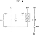
- FIG. 3 illustrates a second example of a circuit configuration of a subpixel.
- a flexible display includes an image processing unit 10, a timing controller 20, a data driver 30, a gate driver 40, and a display panel 50.
- the image processing unit 10 outputs a data signal DATA and a data enable signal DE supplied from the outside.
- the image processing unit 10 may output one or more of a vertical sync signal, a horizontal sync signal, and a clock signal in addition to the data enable signal DE. For the sake of brevity and ease of reading, these signals are not shown.
- the image processing unit 10 is formed on a system circuit board as an integrated circuit (IC).
- the timing controller 20 receives the data signal DATA and driving signals including the data enable signal DE or the vertical sync signal, the horizontal sync signal, the clock signal, etc. from the image processing unit 10.
- the timing controller 20 outputs a gate timing control signal GDC for controlling operation timing of the gate driver 40 and a data timing control signal DDC for controlling operation timing of the data driver 30 based on the driving signals.
- the timing controller 20 may be formed on a control circuit board as an IC.
- the data driver 30 samples and latches the data signal DATA received from the timing controller 20 in response to the data timing control signal DDC supplied from the timing controller 20 and converts the sampled and latched data signal DATA using gamma reference voltages.
- the data driver 30 outputs the converted data signal DATA to data lines DL1 to DLn.
- the data driver 30 is formed on a data circuit substrate as an IC.
- the gate driver 40 outputs a gate signal while shifting a level of a gate voltage in response to the gate timing control signal GDC supplied from the timing controller 20.
- the gate driver 40 outputs the gate signal to gate lines GL1 to GLm.
- the gate driver 40 is formed on a gate circuit board as an IC or is formed on the display panel 50 in a gate-in-panel (GIP) manner.
- the display panel 50 displays an image in response to the data signal DATA and the gate signal respectively received from the data driver 30 and the gate driver 40.
- the display panel 50 includes subpixels SP for displaying an image.
- each subpixel may include a switching transistor SW, a driving transistor DR, a compensation circuit CC, and an organic light emitting diode (OLED).
- the organic light emitting diode operates to emit light based on a driving current generated by the driving transistor DR.
- the switching transistor SW performs a switching operation so that a data signal supplied through a first data line DL1 is stored in a capacitor Cst as a data voltage in response to a gate signal supplied through a first gate line GL1.
- the driving transistor DR enables a driving current to flow between a high potential power line VDD and a low potential power line GND based on the data voltage stored in the capacitor Cst.
- the compensation circuit CC is a circuit for compensating for a threshold voltage of the driving transistor DR.
- a capacitor connected to the switching transistor SW or the driving transistor DR may be mounted inside the compensation circuit CC.
- the compensation circuit CC includes one or more thin film transistors and a capacitor. Configuration of the compensation circuit CC may be variously changed depending on a compensation method. A brief description of the compensation circuit CC will be made.
- a subpixel including the compensation circuit CC may further include a signal line and a power line for driving a compensation TFT and supplying a predetermined signal or electric power.
- the added signal line may be defined as a 1-2 gate line GL1b for driving the compensation TFT included in the subpixel.
- GL1a is a 1-1 gate line for driving the switching transistor SW.
- the added power line may be defined as an initialization power line INIT for initializing a predetermined node of the subpixel to a predetermined voltage.
- this is merely an example, and embodiments are not limited thereto.
- FIGS. 2 and 3 illustrate that one subpixel includes the compensation circuit CC by way of example.
- the compensation circuit CC may be omitted when an object (for example, the data driver 30) to be compensated is positioned outside the subpixel.
- the subpixel has a configuration of 2T(Transistor)1C(Capacitor) in which the switching transistor SW, the driving transistor DR, the capacitor, and the organic light emitting diode are provided.
- the compensation circuit CC when the compensation circuit CC is added to the subpixel, the subpixel may have various configurations such as 3T1C, 4T2C, 5T2C, 6T2C, 7T1C, 7T2C, and the like.
- FIGS. 2 and 3 illustrate that the compensation circuit CC is positioned between the switching transistor SW and the driving transistor DR by way of an example.
- the compensation circuit CC may be further positioned between the driving transistor DR and the organic light emitting diode.
- the position and the structure of the compensation circuit CC are not limited to the ones illustrated in FIGs. 2 and 3 .
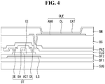
- FIG. 4 is a cross-sectional view of a flexible display according to an embodiment of the disclosure.
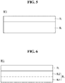
- FIG. 5 schematically illustrates configuration of a first buffer layer according to an embodiment of the disclosure.
- FIG. 6 schematically illustrates configuration of a first buffer layer according to another embodiment of the disclosure.
- a flexible display according to an embodiment of the disclosure includes a thin film transistor DT and an organic light emitting diode OLE on a plastic substrate SUB.
- the plastic substrate SUB may be a polyimide (PI) substrate.
- the flexible display according to the embodiment of the disclosure may have flexible characteristic.
- a first buffer layer BF1 and a second buffer layer BF2 are positioned between the plastic substrate SUB and the thin film transistor DT.
- the first buffer layer BF1 may have a thickness of 100 ⁇ to 11,000 ⁇
- the second buffer layer BF2 may have a thickness of 100 ⁇ to 10,000 ⁇ .
- a light shielding layer LS is positioned between the first buffer layer BF1 and the second buffer layer BF2.
- the light shielding layer LS may be disposed to overlap an active layer ACT, particularly, a channel of the thin film transistor DT and protects an oxide semiconductor element from external light.
- the first buffer layer BF1 blocks ions or impurities diffused from the plastic substrate SUB and prevents the moisture penetration from the outside.
- the first buffer layer BF1 includes a lower layer BL formed of silicon nitride (SiNx) and an upper layer TL formed of silicon oxide (SiOx).
- the lower layer BL and the upper layer TL are sequentially stacked and are positioned between the plastic substrate SUB and the active layer ACT of the thin film transistor DT.
- the lower layer BL is positioned on the plastic substrate SUB.
- the lower layer BL has a thickness capable of performing predetermined barrier characteristics and prevents the moisture penetration through the plastic substrate SUB. Because the lower layer BL is formed of silicon nitride (SiNx), the lower layer BL can satisfy the predetermined barrier characteristics with the thin thickness. Hence, the lower layer BL can prevent an increase in a thickness of the flexible display and secure predetermined flexibility of the flexible display.
- the lower layer BL may have a minimum thickness capable of satisfying the predetermined barrier characteristics. For example, the lower layer BL may have a thickness of 100 ⁇ to 6,000 ⁇ .
- the embodiment of the disclosure sets the SiNx layer (i.e., the lower layer BL), that has the better barrier characteristics than the SiOx layer under the condition of the same thickness, as a layer directly contacting the plastic substrate SUB, thereby simultaneously securing the predetermined barrier characteristics and the predetermined flexibility.
- the SiNx layer i.e., the lower layer BL
- the embodiment of the disclosure directly forms the lower layer BL on the plastic substrate SUB so as to prevent the moisture penetration through the plastic substrate SUB, interface characteristics between the plastic substrate SUB and the lower layer BL need to be considered.
- the embodiment of the disclosure sets the SiNx layer having more similar surface characteristics to the plastic substrate SUB than the SiOx layer as a layer directly contacting the plastic substrate SUB, thereby preventing or minimizing a defective adhesion that may occur at an interface between the plastic substrate SUB and the lower layer BL.
- the embodiment of the disclosure uses not an existing glass substrate but the plastic substrate SUB having relatively low thermal conductivity, an auxiliary means for efficiently dissipating heat generated in an internal driving element, for example, the thin film transistor is necessary.
- the embodiment of the disclosure directly forms the lower layer BL formed of silicon nitride (SiNx) having high thermal conductivity on the plastic substrate SUB, in order to efficiently dissipate heat.
- Thermal conductivity of silicon nitride (SiNx) is approximately 15 times greater than thermal conductivity of silicon oxide (SiOx).
- the embodiment of the disclosure sets the SiNx layer having high thermal conductivity as a layer directly contacting the plastic substrate SUB, thereby efficiently dissipating heat without a separate auxiliary means.
- the upper layer TL is positioned on the lower layer BL.
- the upper layer TL may have a thickness of 100 ⁇ to 5,000 ⁇ .
- the embodiment of the disclosure can relatively increase a length of a moving path of hydrogen existing in the lower layer BL toward the active layer ACT by disposing the upper layer TL between the lower layer BL and the active layer ACT. Further, the embodiment of the disclosure can induce hydrogen diffused from the lower layer BL to move toward not the active layer ACT but the plastic substrate SUB by forming the upper layer TL serving as a barrier on the lower layer BL. Hence, hydrogen diffused from the lower layer BL can move toward the plastic substrate SUB underlying the lower layer BL and can be easily released to the outside.
- the embodiment of the disclosure brings the lower layer BL into contact with the plastic substrate SUB and stacks the upper layer TL on the lower layer BL, thereby preventing or reducing hydrogen from the lower layer BL from entering the active layer ACT. Hence, a reduction in electrical characteristics of the oxide semiconductor can be minimized.
- the thickness of the lower layer BL may be equal to or greater than the thickness of the upper layer TL.
- the lower layer BL may have enough thickness to block foreign substances from the outside.
- the thickness of the upper layer TL may be equal or less than the thickness of the lower layer BL in consideration of the total thickness of the first buffer layer BF1 for the purpose of the flexibility of the flexible display.
- the upper layer TL formed of silicon oxide (SiOx) may have the relatively thin thickness.
- the embodiment of the disclosure can secure the reliability of water vapor transmission (or, water vapor permeation) with the thinner thickness, compared to when the lower layer BL is formed of only silicon oxide (SiOx).
- the embodiment of the disclosure can prevent an increase in the total thickness of the flexible display while securing the barrier characteristics and secure predetermined flexibility of the flexible display.
- the lower layer BL constituting the first buffer layer BF1 may be divided into a first lower layer BL1 and a second lower layer BL2 and dividedly deposited. That is, the first lower layer BL1 and the second lower layer BL2 may be deposited in separate processes. For example, the first lower layer BL1 and the second lower layer BL2 may be sequentially deposited in the same chamber at intervals of predetermined time. Both the first lower layer BL1 and the second lower layer BL2 may be formed of silicon nitride (SiNx).
- the first lower layer BL1 may have a thickness of 100 ⁇ to 3,000 ⁇
- the second lower layer BL2 may have a thickness of 100 ⁇ to 3,000 ⁇ .
- the lower layer BL is not uniformly deposited on the plastic substrate SUB, and thus a thickness variation depending on a position may occur in the lower layer BL. In this instance, surface characteristics of the lower layer BL may be reduced, and the upper layer TL on the lower layer BL may be peeled off.
- CVD chemical vapor deposition
- the embodiment of the disclosure dividedly deposits the lower BL (that is, the first lower layer BL1 and the second lower layer BL2 are deposited in separate processes), thereby reducing the thickness variation of the lower layer BL.
- a corresponding material may be intensively deposited at a specific position during the process, resulting in an excessive thickness variation.
- processes are performed in a temporally and/or spatially separated manner.
- the embodiment of the disclosure can efficiently block a moisture penetration path, that may be formed in the lower layer BL during the process, by dividedly depositing lower layer BL (that is, the first lower layer BL1 and the second lower layer BL2 of the lower layer BL are deposited in separate processes). Namely, micro-sized pores (or fine cracks) may be formed inside the lower layer BL deposited through the CVD process. When the lower layer BL is deposited through a single process, the micro-sized pores formed inside the lower layer BL may be extended in a thickness direction to form a moisture penetration path. On the other hand, when the lower layer BL is dividedly deposited, processes are performed in a temporally and/or spatially separated manner.
- first micro-sized pores are generated in the first lower layer BL1 during a first process and second micro-sized pores are generated in the second lower layer BL2 during a second process, the first micro-sized pores and the second micro-sized pores may be separated from each other without being connected to each other. Therefore, the formation of the moisture penetration path in the thickness direction can be minimized.
- the first lower layer BL1 and the second lower layer BL2 may have different densities.
- the first lower layer BL1 may be formed of silicon nitride (SiNx) having a relatively higher density than the second lower layer BL2 and may have dense characteristics.
- the second lower layer BL2 may be formed of silicon nitride (SiNx) having a relatively lower density than the first lower layer BL1 and may have porous characteristics.
- the embodiment of the disclosure can further improve characteristic of the water vapor permeation by bringing the first lower layer BL1 having the relatively high density into contact with the plastic substrate SUB.
- the second buffer layer BF2 is positioned on the first buffer layer BF1.
- the second buffer layer BF2 functions to prevent the active layer ACT of the thin film transistor DT from being contaminated by impurities and to insulate the light shielding layer LS from the active layer ACT.
- the second buffer layer BF2 is formed of silicon oxide (SiOx).
- the second buffer layer BF2 may have a minimum thickness capable of insulating the light shielding layer LS and the active layer ACT from each other.
- the embodiment of the disclosure can further increase a length of a moving path of hydrogen existing in the lower layer BL toward the active layer ACT by further including the second buffer layer BF2 between the lower layer BL and the active layer ACT. Hence, the embodiment of the disclosure can further reduce hydrogen of the lower layer BL from entering the active layer ACT and minimize a reduction in the electrical characteristics of the oxide semiconductor.
- the thin film transistor DT includes the active layer ACT, a gate electrode GA, a source electrode SE, and a drain electrode DE. More specifically, the active layer ACT is positioned on the second buffer layer BF2.
- the active layer ACT is formed of an oxide semiconductor. Examples of the oxide semiconductor include a zinc oxide semiconductor such as indium gallium zinc oxide (IGZO).
- IGZO indium gallium zinc oxide
- the oxide semiconductor has advantages that it has higher mobility than amorphous silicon and polycrystalline silicon and can be manufactured in a low-temperature process. Because the oxide semiconductor has a low OFF-current, the oxide semiconductor may be suitable for a thin film transistor which has a short ON-time and a long OFF-time. Further, because the oxide semiconductor increases a voltage hold time of the pixel due to the low OFF-current, the oxide semiconductor may be suitable for a display device requiring a low-speed drive and/or low power consumption.
- IGZO indium gallium zinc oxide
- a gate insulating layer GI is positioned on the active layer ACT.
- the gate insulating layer GI insulates the gate electrode GA and may be formed of silicon oxide (SiOx).
- the gate insulating layer GI may not include silicon nitride (SiNx), in order to prevent hydrogen from entering the active layer ACT.
- the gate electrode GA is positioned on the gate insulating layer GI.
- the gate electrode GA may be formed as a single layer or a multilayer formed of one of copper (Cu), molybdenum (Mo), aluminum (Al), chrome (Cr), gold (Au), titanium (Ti), nickel (Ni), neodymium (Nd), tantalum (Ta), and tungsten (W) or a combination thereof.
- the gate electrode GA is positioned corresponding to the channel of the active layer ACT.
- An interlayer dielectric layer ILD is positioned on the gate electrode GA.
- the interlayer dielectric layer ILD insulates the gate electrode GA and the active layer ACT underlying the interlayer dielectric layer ILD.
- the interlayer dielectric layer ILD may be formed as a silicon oxide (SiOx) layer, a silicon nitride (SiNx) layer, or a multilayer thereof. However, the interlayer dielectric layer ILD may not include the SiNx layer, in order to prevent hydrogen from entering the active layer ACT.
- the interlayer dielectric layer ILD has contact holes CH exposing both sides (for example, a source region and a drain region) of the active layer ACT.
- the source electrode SE and the drain electrode DE are positioned on the interlayer dielectric layer ILD.
- Each of the source electrode SE and the drain electrode DE may be formed as a single layer or as a multilayer.
- each of the source electrode SE and the drain electrode DE may be formed of one of molybdenum (Mo), aluminum (Al), chrome (Cr), gold (Au), titanium (Ti), nickel (Ni), neodymium (Nd), and copper (Cu), or a combination thereof.
- each of the source electrode SE and the drain electrode DE may be formed as a double layer of Mo/Al-Nd, Mo/Al, or Ti/Al or as a triple layer of Mo/Al-Nd/Mo, Mo/Al/Mo, or Ti/Al/Ti.
- the source electrode SE and the drain electrode DE are respectively connected to both sides of the active layer ACT through the contact holes CH of the interlayer dielectric layer ILD.
- a passivation layer PAS is positioned on the thin film transistor DT.
- the passivation layer PAS protects the thin film transistor DT and may be formed as a silicon oxide (SiOx) layer, a silicon nitride (SiNx) layer, or a multilayer thereof. However, the passivation layer PAS may not include the SiNx layer, in order to prevent hydrogen from entering the active layer ACT.
- a planarization layer OC is positioned on the passivation layer PAS and reduces a height difference of an underlying structure.
- the planarization layer OC may be formed of an organic material such as photo acryl, polyimide, benzocyclobutene-based resin, and acrylate-based resin.
- One of the passivation layer PAS and the planarization layer OC may be omitted, if necessary or desired.
- the organic light emitting diode OLE is positioned on the planarization layer OC.
- the organic light emitting diode OLE includes a first electrode ANO, an organic light emitting layer OL, and a second electrode CAT. More specifically, the first electrode ANO is positioned on the planarization layer OC.
- the first electrode ANO is connected to the drain electrode DE of the thin film transistor DT through a contact hole penetrating the passivation layer PAS and the planarization layer OC.
- the first electrode ANO may serve as a transmissive electrode formed of a transparent conductive material such as indium tin oxide (ITO), indium zinc oxide (IZO), and zinc oxide (ZnO).
- the first electrode ANO may further include a reflective layer and serve as a reflective electrode.
- the reflective layer may be formed of aluminum (Al), copper (Cu), silver (Ag), nickel (Ni), palladium (Pd) or a combination thereof.
- the reflective layer may be formed of an Ag/Pd/Cu (APC) alloy.
- a bank layer BN defining the pixels is positioned on the plastic substrate SUB including the first electrode ANO.
- the bank layer BN may be formed of an organic material such as polyimide, benzocyclobutene-based resin, and acrylate.
- the organic light emitting layer OL is positioned on the first electrode ANO exposed by the bank layer BN.
- the organic light emitting layer OL is a layer, in which electrons and holes combine and emit light.
- the organic light emitting diode OLE may further include a hole injection layer and/or a hole transport layer between the organic light emitting layer OL and the first electrode ANO, and may further include an electron injection layer and/or an electron transport layer on the organic light emitting layer OL.
- the second electrode CAT is positioned on the organic light emitting layer OL.
- the second electrode CAT may be formed of magnesium (Mg), calcium (Ca), aluminum (Al), silver (Ag), or a combination thereof each having a low work function.
- the second electrode CAT may be thin enough to transmit light and thus may serve as a transmissive electrode. Further, the second electrode CAT may be thick enough to reflect light and thus may serve as a reflective electrode.
- the flexible display according to the embodiment of the disclosure can block ions or impurities diffused from the plastic substrate and prevent the moisture penetration from the outside by forming the buffer layer including the SiNx layer.
- the flexible display according to the embodiment of the disclosure can implement the buffer layer having the thin thickness while securing the predetermined barrier characteristics by using the SiNx layer having a good water vapor transmission rate relative to a thickness.
- the embodiment of the disclosure can provide the flexible display capable of preventing the moisture penetration from the outside while securing the flexibility of the display device.
- the flexible display according to the embodiment of the disclosure can prevent hydrogen included in the SiNx layer from entering the oxide semiconductor by forming the buffer layer including the SiNx layer and the SiOx layer stacked on the SiNx layer.
- the embodiment of the disclosure can prevent a reduction in the electrical characteristics of the oxide semiconductor.
- FIG. 7 schematically illustrates a stacking structure of buffer layers according to a comparative example and an experimental example.
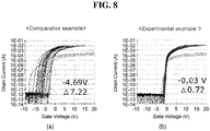
- FIG. 8 is a graph illustrating a current-voltage characteristic of an oxide semiconductor thin film transistor according to a comparative example and an experimental example.
- the following experiments are to examine a change in characteristics of an oxide semiconductor depending on a difference in stacking order of a silicon oxide (SiOx) layer and a silicon nitride (SiNx) layer constituting a first buffer layer between a comparative example and an experimental example, when the first buffer layer according to the comparative example and the first buffer layer according to the experimental example have the same thickness.
- SiOx silicon oxide
- SiNx silicon nitride
- a silicon nitride (SiNx) layer, a silicon oxide (SiOx) layer, and a silicon nitride (SiNx) layer were sequentially stacked on a polyimide (PI) substrate, so that the comparative example was in contrast to the first buffer layer according to the embodiment of the disclosure.
- a thickness of the SiNx layer was 1,000 ⁇ , and a thickness of the SiOx layer was 1,000 ⁇ .
- SiOx silicon oxide
- a thin film transistor including an IGZO active layer was manufactured on the SiOx layer.
- a thickness of the SiOx layer was 3,000 ⁇ .
- a silicon nitride (SiNx) layer, a silicon nitride (SiNx) layer, and a silicon oxide (SiOx) layer constituting the first buffer layer according to the embodiment of the disclosure were sequentially stacked on a polyimide (PI) substrate.
- a thickness of the SiNx layer was 1,000 ⁇ , and a thickness of the SiOx layer was 1,000 ⁇ .
- SiOx silicon oxide
- a thin film transistor including an IGZO active layer was manufactured on the SiOx layer.
- a thickness of the SiOx layer was 3,000 ⁇ .
- FIG. 8 illustrates a result of measuring a current-voltage characteristic of an oxide semiconductor thin film transistor according to the comparative example and the experimental example.
- a threshold voltage of an oxide semiconductor thin film transistor according to the comparative example was shifted by -4.69V in a negative direction and exceeded a normal range. Further, a threshold voltage of an oxide semiconductor thin film transistor according to the experimental example was shifted by -0.03V in the negative direction and was in the normal range.
- the comparative example when the first buffer layer includes the SiNx layer, and the SiNx layer is disposed at an uppermost layer of the first buffer layer, hydrogen existing in the SiNx layer is diffused into the IGZO active layer and changes the device characteristics.
- the first buffer layer includes the SiNx layer, and the SiOx layer is further formed on the SiNx layer as in the experimental example, an amount of hydrogen existing in the SiNx layer entering the IGZO active layer can decrease. Hence, change in the device characteristics can decrease.
- the embodiment of the invention includes the first buffer layer including the SiNx layer and the SiOx layer and disposes the SiOx layer on the SiNx layer in the first buffer layer, thereby securing the reliability of the oxide semiconductor thin film transistor even when the SiNx layer is used.
- a degree of scattering of the threshold voltage in the oxide semiconductor thin film transistor according to the comparative example was ⁇ 7.22 which is beyond a normal range. Further, a degree of scattering of the threshold voltage in the oxide semiconductor thin film transistor according to the experimental example was ⁇ 0.72 which is in the normal range.
- the embodiment of the invention can sufficiently secure a separation distance between the SiNx layer and the oxide semiconductor by disposing the SiOx layer on the SiNx layer in the first buffer layer. Hence, the embodiment of the invention can prevent an influence of the SiNx layer on the oxide semiconductor even when the SiNx layer is formed to have the thickness variation depending on the position, thereby securing the reliability of the components.
Landscapes
- Engineering & Computer Science (AREA)
- Physics & Mathematics (AREA)
- General Physics & Mathematics (AREA)
- Theoretical Computer Science (AREA)
- Microelectronics & Electronic Packaging (AREA)
- Electroluminescent Light Sources (AREA)
- Thin Film Transistor (AREA)
- Devices For Indicating Variable Information By Combining Individual Elements (AREA)
Abstract
Description
- The present disclosure relates to a flexible display.
- With the development of information society, demands for display devices displaying an image are increasing in various ways. In a field of the display devices, a large-sized cathode ray tube (CRT) has been rapidly replaced by a flat panel display (FPD) having advantages of a thin profile, low weight, and a large-sized screen. Examples of the flat panel display include a liquid crystal display (LCD), a plasma display panel (PDP), an organic light emitting diode (OLED) display, and an electrophoresis display (EPD).
- An OLED display includes self-emitting elements capable of emitting light by themselves and has advantages of a fast response time, a high emission efficiency, a high luminance, and a wide viewing angle. In particular, the OLED display may use a flexible plastic substrate. In addition, the OLED display has advantages of a lower driving voltage, lower power consumption, and better color tone as compared to a plasma display panel or an inorganic electroluminescent display.
- The OLED display may include a plurality of buffer layers on a flexible plastic substrate. The plurality of buffer layers blocks ions or impurities diffused from the plastic substrate underlying the buffer layers in a manufacturing process of the OLED display. Further, the plurality of buffer layers blocks the penetration of external moisture from the plastic substrate after the OLED display is completed, thereby preventing the degradation of thin film transistors and organic light emitting diodes.
- However, the buffer layer affects the component adjacent to the buffer layer due to the properties of a material constituting the buffer layer, thereby reducing characteristics of the component. For example, the buffer layer may include silicon nitride (SiNx). When the thin film transistor includes an oxide semiconductor, hydrogen existing in silicon nitride of the buffer layer is diffused and reduces electrical characteristics of the oxide semiconductor.
- The present disclosure is to provide a display device capable of preventing moisture penetration through a plastic substrate.
- The present disclosure is to also provide a flexible display capable of preventing electrical characteristics of an oxide semiconductor from being reduced by a silicon nitride layer constituting a buffer layer.
- In one aspect, there is provided a flexible display including an oxide semiconductor thin film transistor on a plastic substrate, the flexible display including a first buffer layer disposed on the plastic substrate, a second buffer layer disposed on the first buffer layer and formed of silicon oxide (SiOx), and an active layer disposed on the second buffer layer and formed of an oxide semiconductor, wherein the first buffer layer includes a lower layer directly contacting the plastic substrate and formed of silicon nitride (SiNx) and an upper layer disposed on the lower layer and formed of silicon oxide (SiOx).
- In one or more embodiments, a thickness of the lower layer is equal to or greater than a thickness of the upper layer.
- In one or more embodiments, the lower layer includes a first lower layer and a second lower layer that are separated from each other.
- In one or more embodiments, the first lower layer and the second lower layer are formed by separate deposition processes.
- In one or more embodiments, the first lower layer comprises first micro-sized pores and the second lower layer comprises second micro-sized pores, wherein the first micro-sized pores and the second micro-sized pores are separated from each other without being connected to each other.
- In one or more embodiments, the first lower layer has a higher density than the second lower layer.
- In one or more embodiments, the second lower layer is formed on the first lower layer, wherein the first lower layer has dense characteristics and the second lower layer has porous characteristics.
- In one or more embodiments, the flexible display further includes a light shielding layer disposed between the first buffer layer and the second buffer layer and overlapping the active layer.
- The accompanying drawings, which are included to provide a further understanding of the disclosure and are incorporated in and constitute a part of this specification, illustrate aspects of the disclosure and together with the description serve to explain the principles of the disclosure. In the drawings:
-
FIG. 1 is a schematic block diagram of a flexible display according to an embodiment of the disclosure; -
FIG. 2 illustrates a first example of a circuit configuration of a subpixel; -
FIG. 3 illustrates a second example of a circuit configuration of a subpixel; -
FIG. 4 is a cross-sectional view of a flexible display according to an embodiment of the disclosure; -
FIG. 5 schematically illustrates configuration of a first buffer layer according to an embodiment of the disclosure; -
FIG. 6 schematically illustrates configuration of a first buffer layer according to another embodiment of the disclosure; -
FIG. 7 schematically illustrates a stacking structure of buffer layers according to a comparative example and an experimental example; and -
FIG. 8 is a graph illustrating a current-voltage characteristic of an oxide semiconductor thin film transistor according to a comparative example and an experimental example. - Reference will now be made in detail to embodiments of the disclosure, examples of which are illustrated in the accompanying drawings. Wherever possible, the same reference numbers will be used throughout the drawings to refer to the same or like parts. It will be paid attention that detailed description of known arts will be omitted if it is determined that the arts can mislead the embodiments of the disclosure. Names of the respective elements used in the following explanations are selected only for convenience of writing the specification and may be thus different from those used in actual products.
- A display device according to an embodiment of the disclosure is a flexible display in which a display element is formed on a flexible plastic substrate. The flexible display according to the embodiment of the disclosure may be implemented based on a liquid crystal display (LCD), a field emission display (FED), a plasma display panel (PDP), an organic light emitting diode (OLED) display, an electrophoresis display (EPD), a quantum dot display (QDD), and the like. In the following description, for convenience of explanation, a case where the flexible display includes organic light emitting diodes will be described as an example.
- A flexible display includes a first electrode, a second electrode opposite the first electrode, and an emission layer between the first electrode and the second electrode. The first electrode may be an anode electrode, and the second electrode may be a cathode electrode. The flexible display is a self-emission display device configured to form hole-electron pairs, i.e., excitons by combining holes received from the first electrode and electrons received from the second electrode inside the emission layer and emit light by energy generated when the excitons return to a ground level.
- The flexible display according to the embodiment of the disclosure may be applied to both a top emission type display in which light is emitted upwardly, and a bottom emission type display in which light is emitted downwardly. In addition, the flexible display according to the embodiment of the disclosure may be applied to a transparent display in which an object on the back side can be seen through the flexible display.
- The flexible display according to the embodiment of the disclosure uses a plastic substrate, for example, a polyimide (PI) substrate, so as to secure the flexibility of the display device. Because barrier characteristics of the plastic substrate are very low, a buffer layer performing a barrier function has to be added to the plastic substrate. The buffer layer is positioned on the plastic substrate to block ions or impurities diffused from the plastic substrate and to prevent the moisture penetration from the outside.
- In general, the buffer layer may include a silicon oxide (SiOx) layer and a silicon nitride (SiNx) layer. Because the SiOx layer and the SiNx layer each have predetermined barrier characteristics, they can prevent the moisture penetration through the plastic substrate.
- Minimum thicknesses of the SiOx layer and the SiNx layer required to satisfy the predetermined barrier characteristics are different from each other. As a result of actually measuring the minimum thicknesses of the SiOx layer and the SiNx layer capable of satisfying a water vapor transmission rate (WVTR) of 10-2 to 10-4 g/m2/day, the minimum thickness of the SiNx layer was approximately 8 nm, and the minimum thickness of the SiOx layer was approximately 25 nm. Namely, assuming that the SiOx layer and the SiNx layer have the same thickness, it can be seen that the barrier characteristics of the SiNx layer are much better than the barrier characteristics of the SiOx layer.
- The embodiment of the disclosure uses the SiNx layer as the component constituting the buffer layer, considering that i) the SiOx layer has the minimum thickness larger than the SiNx layer so as to satisfy the predetermined barrier characteristics, and ii) the flexibility of the display device is reduced as a thickness of the buffer layer increases.
- However, because the display device according to the embodiment of the disclosure includes a thin film transistor (TFT) using an oxide semiconductor, the embodiment of the disclosure has to prevent hydrogen from entering the oxide semiconductor. Namely, a polycrystalline silicon semiconductor requires a hydrogenation process for filling vacancies of a polycrystalline silicon semiconductor material with hydrogen in consideration of a reduction in device characteristics resulting from the presence of vacancies. On the other hand, because a vacancy, in which a covalent bond is not formed, serves as a carrier in an oxide semiconductor material, the oxide semiconductor material needs to have a certain amount of vacancies. Thus, it is necessary to prevent a large amount of hydrogen from entering the oxide semiconductor.
- More specifically, when the buffer layer includes the SiNx layer, hydrogen existing in the SiNx layer may be diffused into the oxide semiconductor and may change a concentration of carriers inside a channel of the thin film transistor. Hence, a threshold voltage of an oxide semiconductor thin film transistor may be shifted in a negative direction, or the channel of the oxide semiconductor thin film transistor may become conductive, thereby reducing the image quality of the display device. Because of the above problems, a related art display device cannot use a SiNx layer as a buffer layer when including a thin film transistor using an oxide semiconductor.
- The embodiment of the disclosure describes an improved structure in which the SiNx layer can be used as the buffer layer in providing a display device including an oxide semiconductor thin film transistor.
-
FIG. 1 is a schematic block diagram of a flexible display according to an embodiment of the disclosure.FIG. 2 illustrates a first example of a circuit configuration of a subpixel.FIG. 3 illustrates a second example of a circuit configuration of a subpixel. - Referring to
FIG. 1 , a flexible display according to an embodiment of the disclosure includes animage processing unit 10, atiming controller 20, adata driver 30, agate driver 40, and adisplay panel 50. - The
image processing unit 10 outputs a data signal DATA and a data enable signal DE supplied from the outside. Theimage processing unit 10 may output one or more of a vertical sync signal, a horizontal sync signal, and a clock signal in addition to the data enable signal DE. For the sake of brevity and ease of reading, these signals are not shown. Theimage processing unit 10 is formed on a system circuit board as an integrated circuit (IC). - The
timing controller 20 receives the data signal DATA and driving signals including the data enable signal DE or the vertical sync signal, the horizontal sync signal, the clock signal, etc. from theimage processing unit 10. - The
timing controller 20 outputs a gate timing control signal GDC for controlling operation timing of thegate driver 40 and a data timing control signal DDC for controlling operation timing of thedata driver 30 based on the driving signals. Thetiming controller 20 may be formed on a control circuit board as an IC. - The
data driver 30 samples and latches the data signal DATA received from thetiming controller 20 in response to the data timing control signal DDC supplied from thetiming controller 20 and converts the sampled and latched data signal DATA using gamma reference voltages. Thedata driver 30 outputs the converted data signal DATA to data lines DL1 to DLn. Thedata driver 30 is formed on a data circuit substrate as an IC. - The
gate driver 40 outputs a gate signal while shifting a level of a gate voltage in response to the gate timing control signal GDC supplied from thetiming controller 20. Thegate driver 40 outputs the gate signal to gate lines GL1 to GLm. Thegate driver 40 is formed on a gate circuit board as an IC or is formed on thedisplay panel 50 in a gate-in-panel (GIP) manner. - The
display panel 50 displays an image in response to the data signal DATA and the gate signal respectively received from thedata driver 30 and thegate driver 40. Thedisplay panel 50 includes subpixels SP for displaying an image. - As shown in
FIG. 2 , each subpixel may include a switching transistor SW, a driving transistor DR, a compensation circuit CC, and an organic light emitting diode (OLED). The organic light emitting diode operates to emit light based on a driving current generated by the driving transistor DR. - The switching transistor SW performs a switching operation so that a data signal supplied through a first data line DL1 is stored in a capacitor Cst as a data voltage in response to a gate signal supplied through a first gate line GL1. The driving transistor DR enables a driving current to flow between a high potential power line VDD and a low potential power line GND based on the data voltage stored in the capacitor Cst. The compensation circuit CC is a circuit for compensating for a threshold voltage of the driving transistor DR. A capacitor connected to the switching transistor SW or the driving transistor DR may be mounted inside the compensation circuit CC.
- The compensation circuit CC includes one or more thin film transistors and a capacitor. Configuration of the compensation circuit CC may be variously changed depending on a compensation method. A brief description of the compensation circuit CC will be made.
- As shown in
FIG. 3 , a subpixel including the compensation circuit CC may further include a signal line and a power line for driving a compensation TFT and supplying a predetermined signal or electric power. The added signal line may be defined as a 1-2 gate line GL1b for driving the compensation TFT included in the subpixel. InFIG. 3 , "GL1a" is a 1-1 gate line for driving the switching transistor SW. The added power line may be defined as an initialization power line INIT for initializing a predetermined node of the subpixel to a predetermined voltage. However, this is merely an example, and embodiments are not limited thereto. -
FIGS. 2 and3 illustrate that one subpixel includes the compensation circuit CC by way of example. However, the compensation circuit CC may be omitted when an object (for example, the data driver 30) to be compensated is positioned outside the subpixel. The subpixel has a configuration of 2T(Transistor)1C(Capacitor) in which the switching transistor SW, the driving transistor DR, the capacitor, and the organic light emitting diode are provided. However, when the compensation circuit CC is added to the subpixel, the subpixel may have various configurations such as 3T1C, 4T2C, 5T2C, 6T2C, 7T1C, 7T2C, and the like. - Also,
FIGS. 2 and3 illustrate that the compensation circuit CC is positioned between the switching transistor SW and the driving transistor DR by way of an example. However, the compensation circuit CC may be further positioned between the driving transistor DR and the organic light emitting diode. The position and the structure of the compensation circuit CC are not limited to the ones illustrated inFIGs. 2 and3 . -
FIG. 4 is a cross-sectional view of a flexible display according to an embodiment of the disclosure.FIG. 5 schematically illustrates configuration of a first buffer layer according to an embodiment of the disclosure.FIG. 6 schematically illustrates configuration of a first buffer layer according to another embodiment of the disclosure. - Referring to
FIGS. 4 and5 , a flexible display according to an embodiment of the disclosure includes a thin film transistor DT and an organic light emitting diode OLE on a plastic substrate SUB. For example, the plastic substrate SUB may be a polyimide (PI) substrate. Thus, the flexible display according to the embodiment of the disclosure may have flexible characteristic. - A first buffer layer BF1 and a second buffer layer BF2 are positioned between the plastic substrate SUB and the thin film transistor DT. The first buffer layer BF1 may have a thickness of 100 Å to 11,000 Å, and the second buffer layer BF2 may have a thickness of 100 Å to 10,000 Å. A light shielding layer LS is positioned between the first buffer layer BF1 and the second buffer layer BF2. The light shielding layer LS may be disposed to overlap an active layer ACT, particularly, a channel of the thin film transistor DT and protects an oxide semiconductor element from external light.
- The first buffer layer BF1 blocks ions or impurities diffused from the plastic substrate SUB and prevents the moisture penetration from the outside. The first buffer layer BF1 includes a lower layer BL formed of silicon nitride (SiNx) and an upper layer TL formed of silicon oxide (SiOx). The lower layer BL and the upper layer TL are sequentially stacked and are positioned between the plastic substrate SUB and the active layer ACT of the thin film transistor DT.
- The lower layer BL is positioned on the plastic substrate SUB. The lower layer BL has a thickness capable of performing predetermined barrier characteristics and prevents the moisture penetration through the plastic substrate SUB. Because the lower layer BL is formed of silicon nitride (SiNx), the lower layer BL can satisfy the predetermined barrier characteristics with the thin thickness. Hence, the lower layer BL can prevent an increase in a thickness of the flexible display and secure predetermined flexibility of the flexible display. In other words, the lower layer BL may have a minimum thickness capable of satisfying the predetermined barrier characteristics. For example, the lower layer BL may have a thickness of 100 Å to 6,000 Å. The embodiment of the disclosure sets the SiNx layer (i.e., the lower layer BL), that has the better barrier characteristics than the SiOx layer under the condition of the same thickness, as a layer directly contacting the plastic substrate SUB, thereby simultaneously securing the predetermined barrier characteristics and the predetermined flexibility.
- Because the embodiment of the disclosure directly forms the lower layer BL on the plastic substrate SUB so as to prevent the moisture penetration through the plastic substrate SUB, interface characteristics between the plastic substrate SUB and the lower layer BL need to be considered.
- For example, when a SiOx layer is directly formed on the plastic substrate SUB, a peeling may occur at an interface between the plastic substrate SUB and the SiOx layer due to a difference between the properties of the plastic substrate SUB and the SiOx layer. The embodiment of the disclosure sets the SiNx layer having more similar surface characteristics to the plastic substrate SUB than the SiOx layer as a layer directly contacting the plastic substrate SUB, thereby preventing or minimizing a defective adhesion that may occur at an interface between the plastic substrate SUB and the lower layer BL.
- Because the embodiment of the disclosure uses not an existing glass substrate but the plastic substrate SUB having relatively low thermal conductivity, an auxiliary means for efficiently dissipating heat generated in an internal driving element, for example, the thin film transistor is necessary. The embodiment of the disclosure directly forms the lower layer BL formed of silicon nitride (SiNx) having high thermal conductivity on the plastic substrate SUB, in order to efficiently dissipate heat. Thermal conductivity of silicon nitride (SiNx) is approximately 15 times greater than thermal conductivity of silicon oxide (SiOx). The embodiment of the disclosure sets the SiNx layer having high thermal conductivity as a layer directly contacting the plastic substrate SUB, thereby efficiently dissipating heat without a separate auxiliary means.
- The upper layer TL is positioned on the lower layer BL. The upper layer TL may have a thickness of 100 Å to 5,000 Å. The embodiment of the disclosure can relatively increase a length of a moving path of hydrogen existing in the lower layer BL toward the active layer ACT by disposing the upper layer TL between the lower layer BL and the active layer ACT. Further, the embodiment of the disclosure can induce hydrogen diffused from the lower layer BL to move toward not the active layer ACT but the plastic substrate SUB by forming the upper layer TL serving as a barrier on the lower layer BL. Hence, hydrogen diffused from the lower layer BL can move toward the plastic substrate SUB underlying the lower layer BL and can be easily released to the outside. The embodiment of the disclosure brings the lower layer BL into contact with the plastic substrate SUB and stacks the upper layer TL on the lower layer BL, thereby preventing or reducing hydrogen from the lower layer BL from entering the active layer ACT. Hence, a reduction in electrical characteristics of the oxide semiconductor can be minimized.
- The thickness of the lower layer BL may be equal to or greater than the thickness of the upper layer TL. The lower layer BL may have enough thickness to block foreign substances from the outside. Further, the thickness of the upper layer TL may be equal or less than the thickness of the lower layer BL in consideration of the total thickness of the first buffer layer BF1 for the purpose of the flexibility of the flexible display.
- Because ions or impurities diffused from the plastic substrate SUB and moisture from the outside are mostly blocked by the lower layer BL formed of silicon nitride (SiNx), the upper layer TL formed of silicon oxide (SiOx) may have the relatively thin thickness. Namely, the embodiment of the disclosure can secure the reliability of water vapor transmission (or, water vapor permeation) with the thinner thickness, compared to when the lower layer BL is formed of only silicon oxide (SiOx). Namely, the embodiment of the disclosure can prevent an increase in the total thickness of the flexible display while securing the barrier characteristics and secure predetermined flexibility of the flexible display.
- Referring to
FIG. 6 , the lower layer BL constituting the first buffer layer BF1 may be divided into a first lower layer BL1 and a second lower layer BL2 and dividedly deposited. That is, the first lower layer BL1 and the second lower layer BL2 may be deposited in separate processes. For example, the first lower layer BL1 and the second lower layer BL2 may be sequentially deposited in the same chamber at intervals of predetermined time. Both the first lower layer BL1 and the second lower layer BL2 may be formed of silicon nitride (SiNx). The first lower layer BL1 may have a thickness of 100 Å to 3,000 Å, and the second lower layer BL2 may have a thickness of 100 Å to 3,000 Å. - In a chemical vapor deposition (CVD) process, the lower layer BL is not uniformly deposited on the plastic substrate SUB, and thus a thickness variation depending on a position may occur in the lower layer BL. In this instance, surface characteristics of the lower layer BL may be reduced, and the upper layer TL on the lower layer BL may be peeled off.
- The embodiment of the disclosure dividedly deposits the lower BL (that is, the first lower layer BL1 and the second lower layer BL2 are deposited in separate processes), thereby reducing the thickness variation of the lower layer BL. Namely, when the lower layer BL is deposited through a single process, a corresponding material may be intensively deposited at a specific position during the process, resulting in an excessive thickness variation. On the other hand, when the lower layer BL is dividedly deposited, processes are performed in a temporally and/or spatially separated manner. Thus, even if a corresponding material is intensively deposited at a predetermined position during a first process, the position where the material is intensively deposited may be changed during a second process. Therefore, the thickness variation depending on the position can be reduced.
- Further, the embodiment of the disclosure can efficiently block a moisture penetration path, that may be formed in the lower layer BL during the process, by dividedly depositing lower layer BL (that is, the first lower layer BL1 and the second lower layer BL2 of the lower layer BL are deposited in separate processes). Namely, micro-sized pores (or fine cracks) may be formed inside the lower layer BL deposited through the CVD process. When the lower layer BL is deposited through a single process, the micro-sized pores formed inside the lower layer BL may be extended in a thickness direction to form a moisture penetration path. On the other hand, when the lower layer BL is dividedly deposited, processes are performed in a temporally and/or spatially separated manner. Thus, even if first micro-sized pores are generated in the first lower layer BL1 during a first process and second micro-sized pores are generated in the second lower layer BL2 during a second process, the first micro-sized pores and the second micro-sized pores may be separated from each other without being connected to each other. Therefore, the formation of the moisture penetration path in the thickness direction can be minimized.
- The first lower layer BL1 and the second lower layer BL2 may have different densities. The first lower layer BL1 may be formed of silicon nitride (SiNx) having a relatively higher density than the second lower layer BL2 and may have dense characteristics. The second lower layer BL2 may be formed of silicon nitride (SiNx) having a relatively lower density than the first lower layer BL1 and may have porous characteristics. The embodiment of the disclosure can further improve characteristic of the water vapor permeation by bringing the first lower layer BL1 having the relatively high density into contact with the plastic substrate SUB.
- The second buffer layer BF2 is positioned on the first buffer layer BF1. The second buffer layer BF2 functions to prevent the active layer ACT of the thin film transistor DT from being contaminated by impurities and to insulate the light shielding layer LS from the active layer ACT. The second buffer layer BF2 is formed of silicon oxide (SiOx). The second buffer layer BF2 may have a minimum thickness capable of insulating the light shielding layer LS and the active layer ACT from each other.
- The embodiment of the disclosure can further increase a length of a moving path of hydrogen existing in the lower layer BL toward the active layer ACT by further including the second buffer layer BF2 between the lower layer BL and the active layer ACT. Hence, the embodiment of the disclosure can further reduce hydrogen of the lower layer BL from entering the active layer ACT and minimize a reduction in the electrical characteristics of the oxide semiconductor.
- The thin film transistor DT includes the active layer ACT, a gate electrode GA, a source electrode SE, and a drain electrode DE. More specifically, the active layer ACT is positioned on the second buffer layer BF2. The active layer ACT is formed of an oxide semiconductor. Examples of the oxide semiconductor include a zinc oxide semiconductor such as indium gallium zinc oxide (IGZO). The oxide semiconductor has advantages that it has higher mobility than amorphous silicon and polycrystalline silicon and can be manufactured in a low-temperature process. Because the oxide semiconductor has a low OFF-current, the oxide semiconductor may be suitable for a thin film transistor which has a short ON-time and a long OFF-time. Further, because the oxide semiconductor increases a voltage hold time of the pixel due to the low OFF-current, the oxide semiconductor may be suitable for a display device requiring a low-speed drive and/or low power consumption.
- A gate insulating layer GI is positioned on the active layer ACT. The gate insulating layer GI insulates the gate electrode GA and may be formed of silicon oxide (SiOx). The gate insulating layer GI may not include silicon nitride (SiNx), in order to prevent hydrogen from entering the active layer ACT. The gate electrode GA is positioned on the gate insulating layer GI. The gate electrode GA may be formed as a single layer or a multilayer formed of one of copper (Cu), molybdenum (Mo), aluminum (Al), chrome (Cr), gold (Au), titanium (Ti), nickel (Ni), neodymium (Nd), tantalum (Ta), and tungsten (W) or a combination thereof. The gate electrode GA is positioned corresponding to the channel of the active layer ACT. An interlayer dielectric layer ILD is positioned on the gate electrode GA.
- The interlayer dielectric layer ILD insulates the gate electrode GA and the active layer ACT underlying the interlayer dielectric layer ILD. The interlayer dielectric layer ILD may be formed as a silicon oxide (SiOx) layer, a silicon nitride (SiNx) layer, or a multilayer thereof. However, the interlayer dielectric layer ILD may not include the SiNx layer, in order to prevent hydrogen from entering the active layer ACT.
- The interlayer dielectric layer ILD has contact holes CH exposing both sides (for example, a source region and a drain region) of the active layer ACT. The source electrode SE and the drain electrode DE are positioned on the interlayer dielectric layer ILD. Each of the source electrode SE and the drain electrode DE may be formed as a single layer or as a multilayer. When each of the source electrode SE and the drain electrode DE is formed as the single layer, each of the source electrode SE and the drain electrode DE may be formed of one of molybdenum (Mo), aluminum (Al), chrome (Cr), gold (Au), titanium (Ti), nickel (Ni), neodymium (Nd), and copper (Cu), or a combination thereof. When each of the source electrode SE and the drain electrode DE is formed as the multilayer, each of the source electrode SE and the drain electrode DE may be formed as a double layer of Mo/Al-Nd, Mo/Al, or Ti/Al or as a triple layer of Mo/Al-Nd/Mo, Mo/Al/Mo, or Ti/Al/Ti. The source electrode SE and the drain electrode DE are respectively connected to both sides of the active layer ACT through the contact holes CH of the interlayer dielectric layer ILD.
- A passivation layer PAS is positioned on the thin film transistor DT. The passivation layer PAS protects the thin film transistor DT and may be formed as a silicon oxide (SiOx) layer, a silicon nitride (SiNx) layer, or a multilayer thereof. However, the passivation layer PAS may not include the SiNx layer, in order to prevent hydrogen from entering the active layer ACT.
- A planarization layer OC is positioned on the passivation layer PAS and reduces a height difference of an underlying structure. The planarization layer OC may be formed of an organic material such as photo acryl, polyimide, benzocyclobutene-based resin, and acrylate-based resin. One of the passivation layer PAS and the planarization layer OC may be omitted, if necessary or desired.
- The organic light emitting diode OLE is positioned on the planarization layer OC. The organic light emitting diode OLE includes a first electrode ANO, an organic light emitting layer OL, and a second electrode CAT. More specifically, the first electrode ANO is positioned on the planarization layer OC. The first electrode ANO is connected to the drain electrode DE of the thin film transistor DT through a contact hole penetrating the passivation layer PAS and the planarization layer OC. The first electrode ANO may serve as a transmissive electrode formed of a transparent conductive material such as indium tin oxide (ITO), indium zinc oxide (IZO), and zinc oxide (ZnO). Further, the first electrode ANO may further include a reflective layer and serve as a reflective electrode. The reflective layer may be formed of aluminum (Al), copper (Cu), silver (Ag), nickel (Ni), palladium (Pd) or a combination thereof. For example, the reflective layer may be formed of an Ag/Pd/Cu (APC) alloy.
- In addition, a bank layer BN defining the pixels is positioned on the plastic substrate SUB including the first electrode ANO. The bank layer BN may be formed of an organic material such as polyimide, benzocyclobutene-based resin, and acrylate. The organic light emitting layer OL is positioned on the first electrode ANO exposed by the bank layer BN. The organic light emitting layer OL is a layer, in which electrons and holes combine and emit light. The organic light emitting diode OLE may further include a hole injection layer and/or a hole transport layer between the organic light emitting layer OL and the first electrode ANO, and may further include an electron injection layer and/or an electron transport layer on the organic light emitting layer OL.
- The second electrode CAT is positioned on the organic light emitting layer OL. The second electrode CAT may be formed of magnesium (Mg), calcium (Ca), aluminum (Al), silver (Ag), or a combination thereof each having a low work function. The second electrode CAT may be thin enough to transmit light and thus may serve as a transmissive electrode. Further, the second electrode CAT may be thick enough to reflect light and thus may serve as a reflective electrode.
- The flexible display according to the embodiment of the disclosure can block ions or impurities diffused from the plastic substrate and prevent the moisture penetration from the outside by forming the buffer layer including the SiNx layer.
- The flexible display according to the embodiment of the disclosure can implement the buffer layer having the thin thickness while securing the predetermined barrier characteristics by using the SiNx layer having a good water vapor transmission rate relative to a thickness. Thus, the embodiment of the disclosure can provide the flexible display capable of preventing the moisture penetration from the outside while securing the flexibility of the display device.
- The flexible display according to the embodiment of the disclosure can prevent hydrogen included in the SiNx layer from entering the oxide semiconductor by forming the buffer layer including the SiNx layer and the SiOx layer stacked on the SiNx layer. Thus, the embodiment of the disclosure can prevent a reduction in the electrical characteristics of the oxide semiconductor.
- Effects of the flexible display according to the embodiment of the disclosure will be described below through a comparative example and an experimental example. The experiments described below are only examples of the embodiment of the disclosure, and the embodiment of the disclosure is not limited to the following experimental examples.
FIG. 7 schematically illustrates a stacking structure of buffer layers according to a comparative example and an experimental example.FIG. 8 is a graph illustrating a current-voltage characteristic of an oxide semiconductor thin film transistor according to a comparative example and an experimental example. - The following experiments are to examine a change in characteristics of an oxide semiconductor depending on a difference in stacking order of a silicon oxide (SiOx) layer and a silicon nitride (SiNx) layer constituting a first buffer layer between a comparative example and an experimental example, when the first buffer layer according to the comparative example and the first buffer layer according to the experimental example have the same thickness.
- As shown in (a) of
FIG. 7 , a silicon nitride (SiNx) layer, a silicon oxide (SiOx) layer, and a silicon nitride (SiNx) layer were sequentially stacked on a polyimide (PI) substrate, so that the comparative example was in contrast to the first buffer layer according to the embodiment of the disclosure. A thickness of the SiNx layer was 1,000 Å, and a thickness of the SiOx layer was 1,000 Å. - Next, a silicon oxide (SiOx) layer was stacked on the SiNx layer, so that the comparative example was in contrast to the second buffer layer according to the embodiment of the disclosure. A thin film transistor including an IGZO active layer was manufactured on the SiOx layer. A thickness of the SiOx layer was 3,000 Å.
- As shown in (b) of
FIG. 7 , a silicon nitride (SiNx) layer, a silicon nitride (SiNx) layer, and a silicon oxide (SiOx) layer constituting the first buffer layer according to the embodiment of the disclosure were sequentially stacked on a polyimide (PI) substrate. A thickness of the SiNx layer was 1,000 Å, and a thickness of the SiOx layer was 1,000 Å. - Next, a silicon oxide (SiOx) layer constituting the second buffer layer according to the embodiment of the disclosure was stacked, and a thin film transistor including an IGZO active layer was manufactured on the SiOx layer. A thickness of the SiOx layer was 3,000 Å.
-
FIG. 8 illustrates a result of measuring a current-voltage characteristic of an oxide semiconductor thin film transistor according to the comparative example and the experimental example. - Referring to
FIG. 8 , a threshold voltage of an oxide semiconductor thin film transistor according to the comparative example was shifted by -4.69V in a negative direction and exceeded a normal range. Further, a threshold voltage of an oxide semiconductor thin film transistor according to the experimental example was shifted by -0.03V in the negative direction and was in the normal range. - It can be seen from the comparative example that when the first buffer layer includes the SiNx layer, and the SiNx layer is disposed at an uppermost layer of the first buffer layer, hydrogen existing in the SiNx layer is diffused into the IGZO active layer and changes the device characteristics. On the other hand, when the first buffer layer includes the SiNx layer, and the SiOx layer is further formed on the SiNx layer as in the experimental example, an amount of hydrogen existing in the SiNx layer entering the IGZO active layer can decrease. Hence, change in the device characteristics can decrease. Thus, the embodiment of the invention includes the first buffer layer including the SiNx layer and the SiOx layer and disposes the SiOx layer on the SiNx layer in the first buffer layer, thereby securing the reliability of the oxide semiconductor thin film transistor even when the SiNx layer is used.
- Referring again to
FIG. 8 , a degree of scattering of the threshold voltage in the oxide semiconductor thin film transistor according to the comparative example was Δ7.22 which is beyond a normal range. Further, a degree of scattering of the threshold voltage in the oxide semiconductor thin film transistor according to the experimental example was Δ0.72 which is in the normal range. - More specifically, when a thickness variation of the SiNx layer occurs depending on the position in the CVD process, an influence of the SiNx layer on the oxide semiconductor varies depending on the position. As a result, the degree of scattering of the threshold voltage of the oxide semiconductor increases.
- The embodiment of the invention can sufficiently secure a separation distance between the SiNx layer and the oxide semiconductor by disposing the SiOx layer on the SiNx layer in the first buffer layer. Hence, the embodiment of the invention can prevent an influence of the SiNx layer on the oxide semiconductor even when the SiNx layer is formed to have the thickness variation depending on the position, thereby securing the reliability of the components.
- Although aspects have been described with reference to a number of illustrative aspects thereof, it should be understood that numerous other modifications and aspects can be devised by those skilled in the art that will fall within the scope of the principles of this disclosure. More particularly, various variations and modifications are possible in the component parts and/or arrangements of the subject combination arrangement within the scope of the disclosure, the drawings and the appended claims. In addition to variations and modifications in the component parts and/or arrangements, alternative uses will also be apparent to those skilled in the art.
Claims (8)
- A flexible display including an oxide semiconductor thin film transistor (DT) on a plastic substrate (SUB), comprising:a first buffer layer (BF1) disposed on the plastic substrate (SUB);a second buffer layer (BF2) disposed on the first buffer layer (BF1) and formed of silicon oxide; andan active layer (ACT) disposed on the second buffer layer (BF2) and formed of an oxide semiconductor,wherein the first buffer layer (BF1) includes:a lower layer (BL) directly contacting the plastic substrate (SUB) and formed of silicon nitride; andan upper layer (TL) disposed on the lower layer (BL) and formed of silicon oxide.
- The flexible display of claim 1, wherein a thickness of the lower layer (BL) is equal to or greater than a thickness of the upper layer (TL).
- The flexible display of claim 1 or 2, wherein the lower layer (BL) includes a first lower layer (BL1) and a second lower layer (BL2) that are separated from each other.
- The flexible display device of claim 3, wherein the first lower layer (BL1) and the second lower layer (BL2) are formed by separate deposition processes.
- The flexible display device of claim 3 or 4, wherein the first lower layer (BL1) comprises first micro-sized pores and the second lower layer (BL2) comprises second micro-sized pores, wherein the first micro-sized pores and the second micro-sized pores are separated from each other without being connected to each other.
- The flexible display of any one of claims 3 to 5, wherein the first lower layer (BL1) has a higher density than the second lower layer (BL2).
- The flexible display of claim 3 or 4, wherein the second lower layer (BL2) is formed on the first lower layer (BL1), and wherein the first lower layer (BL1) has dense characteristics and the second lower layer (BL2) has porous characteristics.
- The flexible display of any one of claims 1 to 7, further comprising a light shielding layer (LS) disposed between the first buffer layer (BF1) and the second buffer layer (BF2) and overlapping the active layer (ACT).
Applications Claiming Priority (1)
| Application Number | Priority Date | Filing Date | Title |
|---|---|---|---|
| KR1020160122489A KR102832749B1 (en) | 2016-09-23 | 2016-09-23 | Flexible display device |
Publications (2)
| Publication Number | Publication Date |
|---|---|
| EP3300118A1 true EP3300118A1 (en) | 2018-03-28 |
| EP3300118B1 EP3300118B1 (en) | 2020-05-06 |
Family
ID=59955365
Family Applications (1)
| Application Number | Title | Priority Date | Filing Date |
|---|---|---|---|
| EP17191834.5A Active EP3300118B1 (en) | 2016-09-23 | 2017-09-19 | Flexible display |
Country Status (4)
| Country | Link |
|---|---|
| US (1) | US10276723B2 (en) |
| EP (1) | EP3300118B1 (en) |
| KR (1) | KR102832749B1 (en) |
| CN (1) | CN107871750B (en) |
Families Citing this family (10)
| Publication number | Priority date | Publication date | Assignee | Title |
|---|---|---|---|---|
| CN107564922B (en) * | 2017-09-19 | 2020-03-13 | 京东方科技集团股份有限公司 | Array substrate, manufacturing method thereof and display device |
| CN108054186B (en) * | 2017-12-14 | 2021-01-29 | 京东方科技集团股份有限公司 | Flexible array substrate, preparation method and display device |
| US10950436B2 (en) * | 2018-12-05 | 2021-03-16 | Wuhan China Star Optoelectronics Semiconductor Display Technology Co., Ltd. | Array substrate manufacturing using fluorine and hydrogenation processes |
| KR102749086B1 (en) * | 2019-03-14 | 2025-01-03 | 삼성디스플레이 주식회사 | Display device |
| CN111584575A (en) * | 2020-05-14 | 2020-08-25 | 深圳市华星光电半导体显示技术有限公司 | OLED display panel and preparation method |
| KR20220014346A (en) * | 2020-07-23 | 2022-02-07 | 삼성디스플레이 주식회사 | Display device |
| CN111682036B (en) * | 2020-07-31 | 2024-04-19 | 合肥鑫晟光电科技有限公司 | Array substrate, display panel, display device and preparation method of display device |
| EP4120378A1 (en) * | 2021-07-12 | 2023-01-18 | Samsung Display Co., Ltd. | Display device and method of manufacturing the same |
| WO2023062695A1 (en) * | 2021-10-11 | 2023-04-20 | シャープディスプレイテクノロジー株式会社 | Display device |
| KR20230146709A (en) | 2022-04-12 | 2023-10-20 | 삼성디스플레이 주식회사 | Display device and method of manufacturing the display device |
Citations (3)
| Publication number | Priority date | Publication date | Assignee | Title |
|---|---|---|---|---|
| US20040018674A1 (en) * | 2002-07-25 | 2004-01-29 | Chartered Semiconductor Manufacturing Ltd. | Method of fabricating a gate dielectric layer with reduced gate tunnelling current and reduced boron penetration |
| US20160141310A1 (en) * | 2012-08-10 | 2016-05-19 | Samsung Display Co., Ltd. | Thin film transistor substrate and method of manufacturing the same |
| US20160172623A1 (en) * | 2014-12-15 | 2016-06-16 | Lg Display Co., Ltd. | Flexible display device having support layer with rounded edge |
Family Cites Families (14)
| Publication number | Priority date | Publication date | Assignee | Title |
|---|---|---|---|---|
| JP2008276211A (en) * | 2007-04-05 | 2008-11-13 | Fujifilm Corp | Organic electroluminescent display device and patterning method |
| WO2011043195A1 (en) * | 2009-10-09 | 2011-04-14 | Semiconductor Energy Laboratory Co., Ltd. | Semiconductor device |
| KR101862606B1 (en) | 2011-10-05 | 2018-07-06 | 엘지디스플레이 주식회사 | Flexible OLED device |
| JP6108898B2 (en) * | 2013-03-19 | 2017-04-05 | 株式会社東芝 | Display device, thin film transistor, method for manufacturing display device, and method for manufacturing thin film transistor |
| KR102180037B1 (en) * | 2013-11-06 | 2020-11-18 | 삼성디스플레이 주식회사 | Flexible display and manufacturing method thereof |
| US9960280B2 (en) * | 2013-12-26 | 2018-05-01 | Semiconductor Energy Laboratory Co., Ltd. | Semiconductor device |
| US9691799B2 (en) * | 2014-02-24 | 2017-06-27 | Lg Display Co., Ltd. | Thin film transistor substrate and display using the same |
| KR102141082B1 (en) * | 2014-05-02 | 2020-08-05 | 엘지디스플레이 주식회사 | Organic light emitting diode display device and method of fabricating the same |
| KR102230619B1 (en) * | 2014-07-25 | 2021-03-24 | 삼성디스플레이 주식회사 | Thin film transsistor substrate and method for fabricating the same |
| US9544994B2 (en) * | 2014-08-30 | 2017-01-10 | Lg Display Co., Ltd. | Flexible display device with side crack protection structure and manufacturing method for the same |
| TWI699897B (en) * | 2014-11-21 | 2020-07-21 | 日商半導體能源研究所股份有限公司 | Semiconductor device |
| JP6519073B2 (en) * | 2014-12-03 | 2019-05-29 | 株式会社Joled | THIN FILM TRANSISTOR, METHOD FOR MANUFACTURING THE SAME, AND DISPLAY DEVICE |
| KR20160103806A (en) * | 2015-02-25 | 2016-09-02 | 엘에스엠트론 주식회사 | Transparent gas barrier film and method for manufacturing transparent gas barrier film |
| KR102325514B1 (en) * | 2015-02-26 | 2021-11-15 | 삼성디스플레이 주식회사 | Display device and method of manufacturing a display device |
-
2016
- 2016-09-23 KR KR1020160122489A patent/KR102832749B1/en active Active
-
2017
- 2017-09-19 EP EP17191834.5A patent/EP3300118B1/en active Active
- 2017-09-20 CN CN201710853965.9A patent/CN107871750B/en active Active
- 2017-09-25 US US15/714,000 patent/US10276723B2/en active Active
Patent Citations (3)
| Publication number | Priority date | Publication date | Assignee | Title |
|---|---|---|---|---|
| US20040018674A1 (en) * | 2002-07-25 | 2004-01-29 | Chartered Semiconductor Manufacturing Ltd. | Method of fabricating a gate dielectric layer with reduced gate tunnelling current and reduced boron penetration |
| US20160141310A1 (en) * | 2012-08-10 | 2016-05-19 | Samsung Display Co., Ltd. | Thin film transistor substrate and method of manufacturing the same |
| US20160172623A1 (en) * | 2014-12-15 | 2016-06-16 | Lg Display Co., Ltd. | Flexible display device having support layer with rounded edge |
Also Published As
| Publication number | Publication date |
|---|---|
| US20180090617A1 (en) | 2018-03-29 |
| EP3300118B1 (en) | 2020-05-06 |
| KR102832749B1 (en) | 2025-07-10 |
| KR20180033385A (en) | 2018-04-03 |
| US10276723B2 (en) | 2019-04-30 |
| CN107871750B (en) | 2021-08-06 |
| CN107871750A (en) | 2018-04-03 |
Similar Documents
| Publication | Publication Date | Title |
|---|---|---|
| EP3300118B1 (en) | Flexible display | |
| EP3503238B1 (en) | Display device | |
| US10038046B2 (en) | Organic light emitting diode display | |
| KR101309863B1 (en) | Luminescence display and fabricating method thereof | |
| US10950822B2 (en) | Display device capable of improving light extraction efficiency | |
| US10950678B2 (en) | Thin film transistor substrate and organic light-emitting display using the same | |
| KR102268493B1 (en) | Organic light emitting diode device and method of fabricating the same | |
| US10665820B2 (en) | Display device | |
| US20150162399A1 (en) | Semiconductor device, method of manufacturing the same, display unit, and electronic apparatus | |
| KR20120017661A (en) | Organic light emitting display | |
| US20220028963A1 (en) | Organic light emitting display device | |
| KR20170080306A (en) | Organic light emitting display device and method of fabricating the same | |
| KR20120080912A (en) | Organic light emitting display device | |
| KR102565699B1 (en) | Display device and methode for the manufacturing the same | |
| US11222940B2 (en) | Display device including a heat dissipation layer in a curved region | |
| US8669700B2 (en) | Organic light emitting diode display including source and drain electrodes separated from a gate electrode | |
| US12431084B2 (en) | Display device and method of manufacturing same | |
| US10026794B2 (en) | Display device having an insulating pattern covered via and electrode holes | |
| KR20120080913A (en) | Organic light emitting display device | |
| US11626473B2 (en) | Organic light-emitting diode display device having a second electrode with improved electrical contact with a connection electrode in a contact area | |
| KR101936124B1 (en) | Organic Light Emitting Display Device | |
| KR100739645B1 (en) | Organic light emitting display | |
| KR20250164045A (en) | Pixels and display devices including the same | |
| KR20240012892A (en) | Display apparatus | |
| KR20090035840A (en) | Organic light emitting display device |
Legal Events
| Date | Code | Title | Description |
|---|---|---|---|
| PUAI | Public reference made under article 153(3) epc to a published international application that has entered the european phase |
Free format text: ORIGINAL CODE: 0009012 |
|
| STAA | Information on the status of an ep patent application or granted ep patent |
Free format text: STATUS: REQUEST FOR EXAMINATION WAS MADE |
|
| 17P | Request for examination filed |
Effective date: 20170919 |
|
| AK | Designated contracting states |
Kind code of ref document: A1 Designated state(s): AL AT BE BG CH CY CZ DE DK EE ES FI FR GB GR HR HU IE IS IT LI LT LU LV MC MK MT NL NO PL PT RO RS SE SI SK SM TR |
|
| AX | Request for extension of the european patent |
Extension state: BA ME |
|
| RBV | Designated contracting states (corrected) |
Designated state(s): AL AT BE BG CH CY CZ DE DK EE ES FI FR GB GR HR HU IE IS IT LI LT LU LV MC MK MT NL NO PL PT RO RS SE SI SK SM TR |
|
| GRAP | Despatch of communication of intention to grant a patent |
Free format text: ORIGINAL CODE: EPIDOSNIGR1 |
|
| STAA | Information on the status of an ep patent application or granted ep patent |
Free format text: STATUS: GRANT OF PATENT IS INTENDED |
|
| R17P | Request for examination filed (corrected) |
Effective date: 20170919 |
|
| INTG | Intention to grant announced |
Effective date: 20200219 |
|
| GRAS | Grant fee paid |
Free format text: ORIGINAL CODE: EPIDOSNIGR3 |
|
| GRAA | (expected) grant |
Free format text: ORIGINAL CODE: 0009210 |
|
| STAA | Information on the status of an ep patent application or granted ep patent |
Free format text: STATUS: THE PATENT HAS BEEN GRANTED |
|
| AK | Designated contracting states |
Kind code of ref document: B1 Designated state(s): AL AT BE BG CH CY CZ DE DK EE ES FI FR GB GR HR HU IE IS IT LI LT LU LV MC MK MT NL NO PL PT RO RS SE SI SK SM TR |
|
| REG | Reference to a national code |
Ref country code: GB Ref legal event code: FG4D |
|
| REG | Reference to a national code |
Ref country code: CH Ref legal event code: EP Ref country code: AT Ref legal event code: REF Ref document number: 1268218 Country of ref document: AT Kind code of ref document: T Effective date: 20200515 |
|
| REG | Reference to a national code |
Ref country code: IE Ref legal event code: FG4D |
|
| REG | Reference to a national code |
Ref country code: DE Ref legal event code: R096 Ref document number: 602017016091 Country of ref document: DE |
|
| REG | Reference to a national code |
Ref country code: LT Ref legal event code: MG4D |
|
| REG | Reference to a national code |
Ref country code: NL Ref legal event code: MP Effective date: 20200506 |
|
| PG25 | Lapsed in a contracting state [announced via postgrant information from national office to epo] |
Ref country code: SE Free format text: LAPSE BECAUSE OF FAILURE TO SUBMIT A TRANSLATION OF THE DESCRIPTION OR TO PAY THE FEE WITHIN THE PRESCRIBED TIME-LIMIT Effective date: 20200506 Ref country code: PT Free format text: LAPSE BECAUSE OF FAILURE TO SUBMIT A TRANSLATION OF THE DESCRIPTION OR TO PAY THE FEE WITHIN THE PRESCRIBED TIME-LIMIT Effective date: 20200907 Ref country code: FI Free format text: LAPSE BECAUSE OF FAILURE TO SUBMIT A TRANSLATION OF THE DESCRIPTION OR TO PAY THE FEE WITHIN THE PRESCRIBED TIME-LIMIT Effective date: 20200506 Ref country code: IS Free format text: LAPSE BECAUSE OF FAILURE TO SUBMIT A TRANSLATION OF THE DESCRIPTION OR TO PAY THE FEE WITHIN THE PRESCRIBED TIME-LIMIT Effective date: 20200906 Ref country code: NO Free format text: LAPSE BECAUSE OF FAILURE TO SUBMIT A TRANSLATION OF THE DESCRIPTION OR TO PAY THE FEE WITHIN THE PRESCRIBED TIME-LIMIT Effective date: 20200806 Ref country code: GR Free format text: LAPSE BECAUSE OF FAILURE TO SUBMIT A TRANSLATION OF THE DESCRIPTION OR TO PAY THE FEE WITHIN THE PRESCRIBED TIME-LIMIT Effective date: 20200807 Ref country code: LT Free format text: LAPSE BECAUSE OF FAILURE TO SUBMIT A TRANSLATION OF THE DESCRIPTION OR TO PAY THE FEE WITHIN THE PRESCRIBED TIME-LIMIT Effective date: 20200506 |
|
| PG25 | Lapsed in a contracting state [announced via postgrant information from national office to epo] |
Ref country code: LV Free format text: LAPSE BECAUSE OF FAILURE TO SUBMIT A TRANSLATION OF THE DESCRIPTION OR TO PAY THE FEE WITHIN THE PRESCRIBED TIME-LIMIT Effective date: 20200506 Ref country code: BG Free format text: LAPSE BECAUSE OF FAILURE TO SUBMIT A TRANSLATION OF THE DESCRIPTION OR TO PAY THE FEE WITHIN THE PRESCRIBED TIME-LIMIT Effective date: 20200806 Ref country code: RS Free format text: LAPSE BECAUSE OF FAILURE TO SUBMIT A TRANSLATION OF THE DESCRIPTION OR TO PAY THE FEE WITHIN THE PRESCRIBED TIME-LIMIT Effective date: 20200506 Ref country code: HR Free format text: LAPSE BECAUSE OF FAILURE TO SUBMIT A TRANSLATION OF THE DESCRIPTION OR TO PAY THE FEE WITHIN THE PRESCRIBED TIME-LIMIT Effective date: 20200506 |
|
| REG | Reference to a national code |
Ref country code: AT Ref legal event code: MK05 Ref document number: 1268218 Country of ref document: AT Kind code of ref document: T Effective date: 20200506 |
|
| PG25 | Lapsed in a contracting state [announced via postgrant information from national office to epo] |
Ref country code: NL Free format text: LAPSE BECAUSE OF FAILURE TO SUBMIT A TRANSLATION OF THE DESCRIPTION OR TO PAY THE FEE WITHIN THE PRESCRIBED TIME-LIMIT Effective date: 20200506 Ref country code: AL Free format text: LAPSE BECAUSE OF FAILURE TO SUBMIT A TRANSLATION OF THE DESCRIPTION OR TO PAY THE FEE WITHIN THE PRESCRIBED TIME-LIMIT Effective date: 20200506 |
|
| PG25 | Lapsed in a contracting state [announced via postgrant information from national office to epo] |
Ref country code: RO Free format text: LAPSE BECAUSE OF FAILURE TO SUBMIT A TRANSLATION OF THE DESCRIPTION OR TO PAY THE FEE WITHIN THE PRESCRIBED TIME-LIMIT Effective date: 20200506 Ref country code: EE Free format text: LAPSE BECAUSE OF FAILURE TO SUBMIT A TRANSLATION OF THE DESCRIPTION OR TO PAY THE FEE WITHIN THE PRESCRIBED TIME-LIMIT Effective date: 20200506 Ref country code: AT Free format text: LAPSE BECAUSE OF FAILURE TO SUBMIT A TRANSLATION OF THE DESCRIPTION OR TO PAY THE FEE WITHIN THE PRESCRIBED TIME-LIMIT Effective date: 20200506 Ref country code: IT Free format text: LAPSE BECAUSE OF FAILURE TO SUBMIT A TRANSLATION OF THE DESCRIPTION OR TO PAY THE FEE WITHIN THE PRESCRIBED TIME-LIMIT Effective date: 20200506 Ref country code: SM Free format text: LAPSE BECAUSE OF FAILURE TO SUBMIT A TRANSLATION OF THE DESCRIPTION OR TO PAY THE FEE WITHIN THE PRESCRIBED TIME-LIMIT Effective date: 20200506 Ref country code: DK Free format text: LAPSE BECAUSE OF FAILURE TO SUBMIT A TRANSLATION OF THE DESCRIPTION OR TO PAY THE FEE WITHIN THE PRESCRIBED TIME-LIMIT Effective date: 20200506 Ref country code: ES Free format text: LAPSE BECAUSE OF FAILURE TO SUBMIT A TRANSLATION OF THE DESCRIPTION OR TO PAY THE FEE WITHIN THE PRESCRIBED TIME-LIMIT Effective date: 20200506 Ref country code: CZ Free format text: LAPSE BECAUSE OF FAILURE TO SUBMIT A TRANSLATION OF THE DESCRIPTION OR TO PAY THE FEE WITHIN THE PRESCRIBED TIME-LIMIT Effective date: 20200506 |
|
| REG | Reference to a national code |
Ref country code: DE Ref legal event code: R097 Ref document number: 602017016091 Country of ref document: DE |
|
| PG25 | Lapsed in a contracting state [announced via postgrant information from national office to epo] |
Ref country code: SK Free format text: LAPSE BECAUSE OF FAILURE TO SUBMIT A TRANSLATION OF THE DESCRIPTION OR TO PAY THE FEE WITHIN THE PRESCRIBED TIME-LIMIT Effective date: 20200506 Ref country code: PL Free format text: LAPSE BECAUSE OF FAILURE TO SUBMIT A TRANSLATION OF THE DESCRIPTION OR TO PAY THE FEE WITHIN THE PRESCRIBED TIME-LIMIT Effective date: 20200506 |
|
| PLBE | No opposition filed within time limit |
Free format text: ORIGINAL CODE: 0009261 |
|
| STAA | Information on the status of an ep patent application or granted ep patent |
Free format text: STATUS: NO OPPOSITION FILED WITHIN TIME LIMIT |
|
| 26N | No opposition filed |
Effective date: 20210209 |
|
| REG | Reference to a national code |
Ref country code: CH Ref legal event code: PL |
|
| PG25 | Lapsed in a contracting state [announced via postgrant information from national office to epo] |
Ref country code: SI Free format text: LAPSE BECAUSE OF FAILURE TO SUBMIT A TRANSLATION OF THE DESCRIPTION OR TO PAY THE FEE WITHIN THE PRESCRIBED TIME-LIMIT Effective date: 20200506 |
|
| REG | Reference to a national code |
Ref country code: BE Ref legal event code: MM Effective date: 20200930 |
|
| PG25 | Lapsed in a contracting state [announced via postgrant information from national office to epo] |
Ref country code: LU Free format text: LAPSE BECAUSE OF NON-PAYMENT OF DUE FEES Effective date: 20200919 |
|
| PG25 | Lapsed in a contracting state [announced via postgrant information from national office to epo] |
Ref country code: CH Free format text: LAPSE BECAUSE OF NON-PAYMENT OF DUE FEES Effective date: 20200930 Ref country code: BE Free format text: LAPSE BECAUSE OF NON-PAYMENT OF DUE FEES Effective date: 20200930 Ref country code: IE Free format text: LAPSE BECAUSE OF NON-PAYMENT OF DUE FEES Effective date: 20200919 Ref country code: LI Free format text: LAPSE BECAUSE OF NON-PAYMENT OF DUE FEES Effective date: 20200930 |
|
| PG25 | Lapsed in a contracting state [announced via postgrant information from national office to epo] |
Ref country code: TR Free format text: LAPSE BECAUSE OF FAILURE TO SUBMIT A TRANSLATION OF THE DESCRIPTION OR TO PAY THE FEE WITHIN THE PRESCRIBED TIME-LIMIT Effective date: 20200506 Ref country code: MT Free format text: LAPSE BECAUSE OF FAILURE TO SUBMIT A TRANSLATION OF THE DESCRIPTION OR TO PAY THE FEE WITHIN THE PRESCRIBED TIME-LIMIT Effective date: 20200506 Ref country code: CY Free format text: LAPSE BECAUSE OF FAILURE TO SUBMIT A TRANSLATION OF THE DESCRIPTION OR TO PAY THE FEE WITHIN THE PRESCRIBED TIME-LIMIT Effective date: 20200506 |
|
| PG25 | Lapsed in a contracting state [announced via postgrant information from national office to epo] |
Ref country code: MK Free format text: LAPSE BECAUSE OF FAILURE TO SUBMIT A TRANSLATION OF THE DESCRIPTION OR TO PAY THE FEE WITHIN THE PRESCRIBED TIME-LIMIT Effective date: 20200506 Ref country code: MC Free format text: LAPSE BECAUSE OF FAILURE TO SUBMIT A TRANSLATION OF THE DESCRIPTION OR TO PAY THE FEE WITHIN THE PRESCRIBED TIME-LIMIT Effective date: 20200506 |
|
| REG | Reference to a national code |
Ref country code: DE Ref legal event code: R079 Ref document number: 602017016091 Country of ref document: DE Free format text: PREVIOUS MAIN CLASS: H01L0029786000 Ipc: H10D0030670000 |
|
| PGFP | Annual fee paid to national office [announced via postgrant information from national office to epo] |
Ref country code: DE Payment date: 20250721 Year of fee payment: 9 |
|
| PGFP | Annual fee paid to national office [announced via postgrant information from national office to epo] |
Ref country code: GB Payment date: 20250722 Year of fee payment: 9 |
|
| PGFP | Annual fee paid to national office [announced via postgrant information from national office to epo] |
Ref country code: FR Payment date: 20250725 Year of fee payment: 9 |