EP3300086A1 - Method for manufacturing layered bus bar unit - Google Patents
Method for manufacturing layered bus bar unit Download PDFInfo
- Publication number
- EP3300086A1 EP3300086A1 EP16796102.8A EP16796102A EP3300086A1 EP 3300086 A1 EP3300086 A1 EP 3300086A1 EP 16796102 A EP16796102 A EP 16796102A EP 3300086 A1 EP3300086 A1 EP 3300086A1
- Authority
- EP
- European Patent Office
- Prior art keywords
- bus bar
- layer
- electrode terminal
- cured
- bus bars
- Prior art date
- Legal status (The legal status is an assumption and is not a legal conclusion. Google has not performed a legal analysis and makes no representation as to the accuracy of the status listed.)
- Granted
Links
Images


Classifications
-
- B—PERFORMING OPERATIONS; TRANSPORTING
- B32—LAYERED PRODUCTS
- B32B—LAYERED PRODUCTS, i.e. PRODUCTS BUILT-UP OF STRATA OF FLAT OR NON-FLAT, e.g. CELLULAR OR HONEYCOMB, FORM
- B32B7/00—Layered products characterised by the relation between layers; Layered products characterised by the relative orientation of features between layers, or by the relative values of a measurable parameter between layers, i.e. products comprising layers having different physical, chemical or physicochemical properties; Layered products characterised by the interconnection of layers
- B32B7/04—Interconnection of layers
- B32B7/12—Interconnection of layers using interposed adhesives or interposed materials with bonding properties
-
- C—CHEMISTRY; METALLURGY
- C25—ELECTROLYTIC OR ELECTROPHORETIC PROCESSES; APPARATUS THEREFOR
- C25D—PROCESSES FOR THE ELECTROLYTIC OR ELECTROPHORETIC PRODUCTION OF COATINGS; ELECTROFORMING; APPARATUS THEREFOR
- C25D13/00—Electrophoretic coating characterised by the process
- C25D13/04—Electrophoretic coating characterised by the process with organic material
-
- B—PERFORMING OPERATIONS; TRANSPORTING
- B32—LAYERED PRODUCTS
- B32B—LAYERED PRODUCTS, i.e. PRODUCTS BUILT-UP OF STRATA OF FLAT OR NON-FLAT, e.g. CELLULAR OR HONEYCOMB, FORM
- B32B15/00—Layered products comprising a layer of metal
- B32B15/04—Layered products comprising a layer of metal comprising metal as the main or only constituent of a layer, which is next to another layer of the same or of a different material
- B32B15/08—Layered products comprising a layer of metal comprising metal as the main or only constituent of a layer, which is next to another layer of the same or of a different material of synthetic resin
-
- B—PERFORMING OPERATIONS; TRANSPORTING
- B32—LAYERED PRODUCTS
- B32B—LAYERED PRODUCTS, i.e. PRODUCTS BUILT-UP OF STRATA OF FLAT OR NON-FLAT, e.g. CELLULAR OR HONEYCOMB, FORM
- B32B15/00—Layered products comprising a layer of metal
- B32B15/04—Layered products comprising a layer of metal comprising metal as the main or only constituent of a layer, which is next to another layer of the same or of a different material
- B32B15/08—Layered products comprising a layer of metal comprising metal as the main or only constituent of a layer, which is next to another layer of the same or of a different material of synthetic resin
- B32B15/088—Layered products comprising a layer of metal comprising metal as the main or only constituent of a layer, which is next to another layer of the same or of a different material of synthetic resin comprising polyamides
-
- B—PERFORMING OPERATIONS; TRANSPORTING
- B32—LAYERED PRODUCTS
- B32B—LAYERED PRODUCTS, i.e. PRODUCTS BUILT-UP OF STRATA OF FLAT OR NON-FLAT, e.g. CELLULAR OR HONEYCOMB, FORM
- B32B15/00—Layered products comprising a layer of metal
- B32B15/04—Layered products comprising a layer of metal comprising metal as the main or only constituent of a layer, which is next to another layer of the same or of a different material
- B32B15/08—Layered products comprising a layer of metal comprising metal as the main or only constituent of a layer, which is next to another layer of the same or of a different material of synthetic resin
- B32B15/092—Layered products comprising a layer of metal comprising metal as the main or only constituent of a layer, which is next to another layer of the same or of a different material of synthetic resin comprising epoxy resins
-
- B—PERFORMING OPERATIONS; TRANSPORTING
- B32—LAYERED PRODUCTS
- B32B—LAYERED PRODUCTS, i.e. PRODUCTS BUILT-UP OF STRATA OF FLAT OR NON-FLAT, e.g. CELLULAR OR HONEYCOMB, FORM
- B32B27/00—Layered products comprising a layer of synthetic resin
- B32B27/06—Layered products comprising a layer of synthetic resin as the main or only constituent of a layer, which is next to another layer of the same or of a different material
-
- B—PERFORMING OPERATIONS; TRANSPORTING
- B32—LAYERED PRODUCTS
- B32B—LAYERED PRODUCTS, i.e. PRODUCTS BUILT-UP OF STRATA OF FLAT OR NON-FLAT, e.g. CELLULAR OR HONEYCOMB, FORM
- B32B27/00—Layered products comprising a layer of synthetic resin
- B32B27/28—Layered products comprising a layer of synthetic resin comprising synthetic resins not wholly covered by any one of the sub-groups B32B27/30 - B32B27/42
- B32B27/281—Layered products comprising a layer of synthetic resin comprising synthetic resins not wholly covered by any one of the sub-groups B32B27/30 - B32B27/42 comprising polyimides
-
- B—PERFORMING OPERATIONS; TRANSPORTING
- B32—LAYERED PRODUCTS
- B32B—LAYERED PRODUCTS, i.e. PRODUCTS BUILT-UP OF STRATA OF FLAT OR NON-FLAT, e.g. CELLULAR OR HONEYCOMB, FORM
- B32B27/00—Layered products comprising a layer of synthetic resin
- B32B27/34—Layered products comprising a layer of synthetic resin comprising polyamides
-
- B—PERFORMING OPERATIONS; TRANSPORTING
- B32—LAYERED PRODUCTS
- B32B—LAYERED PRODUCTS, i.e. PRODUCTS BUILT-UP OF STRATA OF FLAT OR NON-FLAT, e.g. CELLULAR OR HONEYCOMB, FORM
- B32B27/00—Layered products comprising a layer of synthetic resin
- B32B27/38—Layered products comprising a layer of synthetic resin comprising epoxy resins
-
- C—CHEMISTRY; METALLURGY
- C25—ELECTROLYTIC OR ELECTROPHORETIC PROCESSES; APPARATUS THEREFOR
- C25D—PROCESSES FOR THE ELECTROLYTIC OR ELECTROPHORETIC PRODUCTION OF COATINGS; ELECTROFORMING; APPARATUS THEREFOR
- C25D13/00—Electrophoretic coating characterised by the process
- C25D13/12—Electrophoretic coating characterised by the process characterised by the article coated
-
- C—CHEMISTRY; METALLURGY
- C25—ELECTROLYTIC OR ELECTROPHORETIC PROCESSES; APPARATUS THEREFOR
- C25D—PROCESSES FOR THE ELECTROLYTIC OR ELECTROPHORETIC PRODUCTION OF COATINGS; ELECTROFORMING; APPARATUS THEREFOR
- C25D13/00—Electrophoretic coating characterised by the process
- C25D13/22—Servicing or operating apparatus or multistep processes
-
- H—ELECTRICITY
- H01—ELECTRIC ELEMENTS
- H01B—CABLES; CONDUCTORS; INSULATORS; SELECTION OF MATERIALS FOR THEIR CONDUCTIVE, INSULATING OR DIELECTRIC PROPERTIES
- H01B13/00—Apparatus or processes specially adapted for manufacturing conductors or cables
- H01B13/0036—Details
-
- B—PERFORMING OPERATIONS; TRANSPORTING
- B32—LAYERED PRODUCTS
- B32B—LAYERED PRODUCTS, i.e. PRODUCTS BUILT-UP OF STRATA OF FLAT OR NON-FLAT, e.g. CELLULAR OR HONEYCOMB, FORM
- B32B37/00—Methods or apparatus for laminating, e.g. by curing or by ultrasonic bonding
- B32B37/14—Methods or apparatus for laminating, e.g. by curing or by ultrasonic bonding characterised by the properties of the layers
- B32B37/24—Methods or apparatus for laminating, e.g. by curing or by ultrasonic bonding characterised by the properties of the layers with at least one layer not being coherent before laminating, e.g. made up from granular material sprinkled onto a substrate
- B32B2037/243—Coating
-
- B—PERFORMING OPERATIONS; TRANSPORTING
- B32—LAYERED PRODUCTS
- B32B—LAYERED PRODUCTS, i.e. PRODUCTS BUILT-UP OF STRATA OF FLAT OR NON-FLAT, e.g. CELLULAR OR HONEYCOMB, FORM
- B32B38/00—Ancillary operations in connection with laminating processes
- B32B2038/0052—Other operations not otherwise provided for
- B32B2038/0076—Curing, vulcanising, cross-linking
-
- B—PERFORMING OPERATIONS; TRANSPORTING
- B32—LAYERED PRODUCTS
- B32B—LAYERED PRODUCTS, i.e. PRODUCTS BUILT-UP OF STRATA OF FLAT OR NON-FLAT, e.g. CELLULAR OR HONEYCOMB, FORM
- B32B2250/00—Layers arrangement
- B32B2250/03—3 layers
-
- B—PERFORMING OPERATIONS; TRANSPORTING
- B32—LAYERED PRODUCTS
- B32B—LAYERED PRODUCTS, i.e. PRODUCTS BUILT-UP OF STRATA OF FLAT OR NON-FLAT, e.g. CELLULAR OR HONEYCOMB, FORM
- B32B2250/00—Layers arrangement
- B32B2250/44—Number of layers variable across the laminate
-
- B—PERFORMING OPERATIONS; TRANSPORTING
- B32—LAYERED PRODUCTS
- B32B—LAYERED PRODUCTS, i.e. PRODUCTS BUILT-UP OF STRATA OF FLAT OR NON-FLAT, e.g. CELLULAR OR HONEYCOMB, FORM
- B32B2255/00—Coating on the layer surface
- B32B2255/06—Coating on the layer surface on metal layer
-
- B—PERFORMING OPERATIONS; TRANSPORTING
- B32—LAYERED PRODUCTS
- B32B—LAYERED PRODUCTS, i.e. PRODUCTS BUILT-UP OF STRATA OF FLAT OR NON-FLAT, e.g. CELLULAR OR HONEYCOMB, FORM
- B32B2255/00—Coating on the layer surface
- B32B2255/26—Polymeric coating
-
- B—PERFORMING OPERATIONS; TRANSPORTING
- B32—LAYERED PRODUCTS
- B32B—LAYERED PRODUCTS, i.e. PRODUCTS BUILT-UP OF STRATA OF FLAT OR NON-FLAT, e.g. CELLULAR OR HONEYCOMB, FORM
- B32B2307/00—Properties of the layers or laminate
- B32B2307/20—Properties of the layers or laminate having particular electrical or magnetic properties, e.g. piezoelectric
- B32B2307/202—Conductive
-
- B—PERFORMING OPERATIONS; TRANSPORTING
- B32—LAYERED PRODUCTS
- B32B—LAYERED PRODUCTS, i.e. PRODUCTS BUILT-UP OF STRATA OF FLAT OR NON-FLAT, e.g. CELLULAR OR HONEYCOMB, FORM
- B32B2307/00—Properties of the layers or laminate
- B32B2307/20—Properties of the layers or laminate having particular electrical or magnetic properties, e.g. piezoelectric
- B32B2307/206—Insulating
-
- B—PERFORMING OPERATIONS; TRANSPORTING
- B32—LAYERED PRODUCTS
- B32B—LAYERED PRODUCTS, i.e. PRODUCTS BUILT-UP OF STRATA OF FLAT OR NON-FLAT, e.g. CELLULAR OR HONEYCOMB, FORM
- B32B2307/00—Properties of the layers or laminate
- B32B2307/30—Properties of the layers or laminate having particular thermal properties
- B32B2307/306—Resistant to heat
-
- B—PERFORMING OPERATIONS; TRANSPORTING
- B32—LAYERED PRODUCTS
- B32B—LAYERED PRODUCTS, i.e. PRODUCTS BUILT-UP OF STRATA OF FLAT OR NON-FLAT, e.g. CELLULAR OR HONEYCOMB, FORM
- B32B2307/00—Properties of the layers or laminate
- B32B2307/50—Properties of the layers or laminate having particular mechanical properties
- B32B2307/54—Yield strength; Tensile strength
-
- B—PERFORMING OPERATIONS; TRANSPORTING
- B32—LAYERED PRODUCTS
- B32B—LAYERED PRODUCTS, i.e. PRODUCTS BUILT-UP OF STRATA OF FLAT OR NON-FLAT, e.g. CELLULAR OR HONEYCOMB, FORM
- B32B2307/00—Properties of the layers or laminate
- B32B2307/50—Properties of the layers or laminate having particular mechanical properties
- B32B2307/542—Shear strength
-
- B—PERFORMING OPERATIONS; TRANSPORTING
- B32—LAYERED PRODUCTS
- B32B—LAYERED PRODUCTS, i.e. PRODUCTS BUILT-UP OF STRATA OF FLAT OR NON-FLAT, e.g. CELLULAR OR HONEYCOMB, FORM
- B32B2311/00—Metals, their alloys or their compounds
-
- B—PERFORMING OPERATIONS; TRANSPORTING
- B32—LAYERED PRODUCTS
- B32B—LAYERED PRODUCTS, i.e. PRODUCTS BUILT-UP OF STRATA OF FLAT OR NON-FLAT, e.g. CELLULAR OR HONEYCOMB, FORM
- B32B2457/00—Electrical equipment
-
- C—CHEMISTRY; METALLURGY
- C09—DYES; PAINTS; POLISHES; NATURAL RESINS; ADHESIVES; COMPOSITIONS NOT OTHERWISE PROVIDED FOR; APPLICATIONS OF MATERIALS NOT OTHERWISE PROVIDED FOR
- C09D—COATING COMPOSITIONS, e.g. PAINTS, VARNISHES OR LACQUERS; FILLING PASTES; CHEMICAL PAINT OR INK REMOVERS; INKS; CORRECTING FLUIDS; WOODSTAINS; PASTES OR SOLIDS FOR COLOURING OR PRINTING; USE OF MATERIALS THEREFOR
- C09D5/00—Coating compositions, e.g. paints, varnishes or lacquers, characterised by their physical nature or the effects produced; Filling pastes
- C09D5/44—Coating compositions, e.g. paints, varnishes or lacquers, characterised by their physical nature or the effects produced; Filling pastes for electrophoretic applications
-
- H—ELECTRICITY
- H01—ELECTRIC ELEMENTS
- H01B—CABLES; CONDUCTORS; INSULATORS; SELECTION OF MATERIALS FOR THEIR CONDUCTIVE, INSULATING OR DIELECTRIC PROPERTIES
- H01B3/00—Insulators or insulating bodies characterised by the insulating materials; Selection of materials for their insulating or dielectric properties
- H01B3/18—Insulators or insulating bodies characterised by the insulating materials; Selection of materials for their insulating or dielectric properties mainly consisting of organic substances
- H01B3/30—Insulators or insulating bodies characterised by the insulating materials; Selection of materials for their insulating or dielectric properties mainly consisting of organic substances plastics; resins; waxes
-
- H—ELECTRICITY
- H01—ELECTRIC ELEMENTS
- H01B—CABLES; CONDUCTORS; INSULATORS; SELECTION OF MATERIALS FOR THEIR CONDUCTIVE, INSULATING OR DIELECTRIC PROPERTIES
- H01B3/00—Insulators or insulating bodies characterised by the insulating materials; Selection of materials for their insulating or dielectric properties
- H01B3/18—Insulators or insulating bodies characterised by the insulating materials; Selection of materials for their insulating or dielectric properties mainly consisting of organic substances
- H01B3/30—Insulators or insulating bodies characterised by the insulating materials; Selection of materials for their insulating or dielectric properties mainly consisting of organic substances plastics; resins; waxes
- H01B3/303—Macromolecular compounds obtained by reactions forming a linkage containing nitrogen with or without oxygen or carbon in the main chain of the macromolecule, not provided for in groups H01B3/38 or H01B3/302
- H01B3/305—Polyamides or polyesteramides
-
- H—ELECTRICITY
- H01—ELECTRIC ELEMENTS
- H01B—CABLES; CONDUCTORS; INSULATORS; SELECTION OF MATERIALS FOR THEIR CONDUCTIVE, INSULATING OR DIELECTRIC PROPERTIES
- H01B3/00—Insulators or insulating bodies characterised by the insulating materials; Selection of materials for their insulating or dielectric properties
- H01B3/18—Insulators or insulating bodies characterised by the insulating materials; Selection of materials for their insulating or dielectric properties mainly consisting of organic substances
- H01B3/30—Insulators or insulating bodies characterised by the insulating materials; Selection of materials for their insulating or dielectric properties mainly consisting of organic substances plastics; resins; waxes
- H01B3/303—Macromolecular compounds obtained by reactions forming a linkage containing nitrogen with or without oxygen or carbon in the main chain of the macromolecule, not provided for in groups H01B3/38 or H01B3/302
- H01B3/306—Polyimides or polyesterimides
-
- H—ELECTRICITY
- H01—ELECTRIC ELEMENTS
- H01B—CABLES; CONDUCTORS; INSULATORS; SELECTION OF MATERIALS FOR THEIR CONDUCTIVE, INSULATING OR DIELECTRIC PROPERTIES
- H01B3/00—Insulators or insulating bodies characterised by the insulating materials; Selection of materials for their insulating or dielectric properties
- H01B3/18—Insulators or insulating bodies characterised by the insulating materials; Selection of materials for their insulating or dielectric properties mainly consisting of organic substances
- H01B3/30—Insulators or insulating bodies characterised by the insulating materials; Selection of materials for their insulating or dielectric properties mainly consisting of organic substances plastics; resins; waxes
- H01B3/40—Insulators or insulating bodies characterised by the insulating materials; Selection of materials for their insulating or dielectric properties mainly consisting of organic substances plastics; resins; waxes epoxy resins
-
- H—ELECTRICITY
- H02—GENERATION; CONVERSION OR DISTRIBUTION OF ELECTRIC POWER
- H02G—INSTALLATION OF ELECTRIC CABLES OR LINES, OR OF COMBINED OPTICAL AND ELECTRIC CABLES OR LINES
- H02G5/00—Installations of bus-bars
- H02G5/005—Laminated bus-bars
Definitions
- the present invention relates to a method for producing a multi-layer bus bar unit, and more particularly relates to a method for producing a multi-layer bus bar unit in which a plurality of metal bodies (electric conductors) running parallel to each other are covered with resin covering layers.
- Patent Literature 1 An example of a conventional multi-layer bus bar unit of this type is shown in Patent Literature 1 disclosed under the title of "MULTI-LAYER BUS BAR ASSEMBLY AND MOLDING DEVICE FOR THE SAME.”
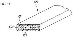
- a disclosed multi-layer bus bar assembly 100 includes: flat plate-shaped conductors (bus bars) 101 and 102 running parallel to each other face-to-face; and a resin molded part 103 that fills a gap between the bus bars 101 and 102 and covers all circumferences of the respective bus bars 101 and 102.
- Patent Literature 1 Japanese Patent Application Laid-Open No: 2007-215340
- the bus bars 101 and 102 set in a cavity formed by an upper mold and a lower mold are subjected to insert injection molding with a molding resin to form the resin molded part 103.
- a new mold needs to be designed and manufactured. Therefore, it may take time from the designing to launching of a product, thereby missing the timing to commercialize the product.
- initial introduction costs including a cost for designing and manufacturing the mold are increased, thus leading to increase in the production costs.
- the present invention has been made in view of the above-described problems and it is an object of the present invention to provide a multi-layer bus bar unit capable of: easily coping with a demand for a multi-layer bus bar assembly (referred to as a "multi-layer bus bar unit" in the present invention) having different specifications such as a shape and dimensions; reducing an amount of time required before launching a product; reducing production costs including initial introduction costs such as a cost for designing and manufacturing a die; and ensuring long-term reliability including electrical and temporal reliability.
- an invention as set forth in claim 1 of the present invention provides a method for producing a multi-layer bus bar unit having a multi-layer structure including a plurality of bus bars.
- the method includes the steps of: preparing a plurality of metal flat plate-shaped bus bars each having electrode terminal parts at two or more locations; depositing a coating film over an entire surface of each of the plurality of bus bars by electrodeposition coating with an electrodeposition coating material having heat resistance and insulation properties; subjecting a coating film of a predetermined bus bar among the plurality of bus bars with the coating films to a heating treatment, so that the coating film of the predetermined bus bar is completely cured; subjecting a bus bar other than the predetermined bus bar among the plurality of bus bars with the coating films to a heat treatment so that the bus bar other than the predetermined bus bar is semi-cured; and obtaining the multi-layer structure by alternately overlapping, and then subjecting to a pressure and heating treatment, the bus bar having the completely-cured coating film and the bus bar having the semi-cured coating film
- An invention as set forth in claim 2 of the present invention is characterized in that the electrodeposition coating material in claim 1 is any of polyimide, polyamide, epoxy, and polyamidimide.
- An invention as set forth in claim 3 of the present invention is characterized in that a step of applying masking to the electrode terminal parts of each of the plurality of bus bars is provided before the step of depositing the coating films, and a step of removing the masking and thereby exposing the electrode terminal parts is provided after the step of obtaining the multi-layer structure in any of claim 1 or claim 2.
- An invention as set forth in claim 4 of the present invention is characterized in that a step of removing the completely-cured coating films covering the electrode terminal parts and thereby exposing the electrode terminal parts is provided after the step of obtaining the multi-layer structure in any of claim 1 or claim 2.
- An invention as set forth in claim 5 of the present invention provides a method for producing a multi-layer bus bar unit having a multi-layer structure including a plurality of bus bars.
- the method includes the steps of: preparing a plurality of metal flat plate-shaped bus bars each having electrode terminal parts at two or more locations; depositing a coating film over an entire surface of each of the plurality of bus bars by electrodeposition coating with an electrodeposition coating material having heat resistance and insulation properties; subjecting the plurality of bus bars with the coating films to a heating treatment, so that the plurality of bus bars are semi-cured; and obtaining the multi-layer structure by overlapping, and then subjecting to a pressure and heating treatment, the bus bars having the semi-cured coating films with a space retention member being interposed therebetween, so that the semi-cured coating films are completely cured and the plurality of bus bars adhere to each other by the completely-cured coating films.
- An invention as set forth in claim 6 of the present invention is characterized in that the electrodeposition coating material in claim 5 is any of polyimide, polyamide, epoxy, and polyamidimide.
- An invention as set forth in claim 7 of the present invention is characterized in that the space retention member in any of claim 5 or claim 6 is any of a glass bead, a silica bead, and a sheet material of the same kind as the electrodeposition coating material.
- An invention as set forth in claim 8 of the present invention is characterized in that a step of applying masking to the electrode terminal parts of each of the plurality of bus bars is provided before the step of depositing the coating films, and a step of removing the masking and thereby exposing the electrode terminal parts is provided after the step of obtaining the multi-layer structure in any one of claims 5 to 7.
- An invention as set forth in claim 9 of the present invention is characterized in that a step of removing the completely-cured coating films covering the electrode terminal parts and thereby exposing the electrode terminal parts is provided after the step of obtaining the multi-layer structure in any one of claims 5 to 7.
- the coating film of the predetermined bus bar among the plurality of bus bars with the coating films formed by electrodeposition coating is completely cured, and the coating film of the bus bar other than the predetermined bus bar is semi-cured.
- the bus bar having the completely-cured coating film and the bus bar having the semi-cured coating film are overlapped alternately, and the semi-cured coating film is completely cured.
- the multi-layer bus bar unit having the multi-layer structure in which the plurality of bus bars adhere to each other by the completely-cured coating film is fabricated.
- a press die for punching a bus bar is generally only one component newly required to commercialize a product coping with a demand for different specifications.
- production costs including initial costs such as a cost for manufacturing a die can be reduced.
- the coating films never experience, because of their production method, the occurrence of defects such as a weld line or a short, which may be generated in the injection molding. In addition, the occurrence of voids can be reduced sufficiently.
- a coating material having a high heat resistance property and a high mechanical strength such as polyimide, polyamide, epoxy, or preferably polyamidimide, is used in the electrodeposition coating. Consequently, the occurrence of defects such as separation caused by stress applied during use or thermal history can be reduced sufficiently, thereby ensuring long-term reliability including electrical and temporal reliability.
- FIGS. 1 to 10 identical parts will be denoted by the same reference numerals.
- the embodiments to be described below are preferred specific examples of the present invention, and thus include technically-preferred various limitations.
- the scope of the present invention is not limited to these embodiments unless explicitly stated in the following description that the present invention is limited thereby.
- FIG. 1 is an explanatory diagram showing a multi-layer bus bar unit of a first embodiment according to the present invention.
- FIG. 1(a) is a plan view
- FIG. 1(b) is a cross-sectional view taken along line A-A in FIG. 1(a) .
- a multi-layer bus bar unit 1 of the present embodiment two bus bars, i.e., a first bus bar 10 and a second bus bar 20 each formed from a metal member, are covered with resin covering layers 12 and 22 formed from polyimide, polyamide, epoxy, or preferably polyamidimide having excellent heat resistance and insulation properties.
- the bus bars 10 and 20 adhere to each other by the resin covering layers 12 and 22 to form the multi-layer bus bar unit 1 having a two-layer structure.
- the first bus bar 10 constituting the multi-layer bus bar unit 1 has: an extended part 10a having a long plate shape; and a pair of electrode terminal parts 10b and 10c protruding in a direction substantially perpendicular to an extended direction from respective ends of the extended part 10a.
- the second bus bar 20 constituting the multi-layer bus bar unit 1 has: an extended part 20a having a long plate shape; and a pair of electrode terminal parts 20b and 20c protruding in a direction substantially perpendicular to an extended direction from respective ends of the extended part 20a.
- the extended part 10a of the first bus bar 10 and the extended part 20a of the second bus bar 20 each function as a current path (power path).
- a current path power path
- one set of the electrode terminal parts 10b and 10c in the first bus bar 10 and the electrode terminal parts 20b and 20c in the second bus bar 20 are connected to a positive electrode and a negative electrode of an external power source and function to receive externally-supplied power
- the other set of the electrode terminal parts 10c and 20c are connected to a positive electrode and a negative electrode of an external device and function to feed the power having passed through the first bus bar 10 and the second bus bar 20 to the external device.
- first bus bar 10 and the second bus bar 20 have substantially the same outline and dimensions, and have a positional relationship in which the first bus bar 10 and the second bus bar 20 are disposed face-to-face while being displaced relative to each other in a longitudinal direction thereof.
- the first bus bar 10 and the second bus bar 20 run parallel to each other with the extended parts 10a and 20a facing each other with a uniform predetermined interval therebetween.
- the first bus bar 10 and the second bus bar 20 are covered with the resin covering layers 12 and 22 over the entire surfaces thereof excluding the pair of electrode terminal parts 10b and 10c in the first bus bar 10 and the pair of electrode terminal parts 20b and 20c in the second bus bar 20.
- the gap between the extended parts 10a and 20a running parallel to each other is filled also with the resin covering layers 12 and 22, so that the extended parts 10a and 20a adhere to each other via the resin covering layers 12 and 22.
- bus bars i.e., the flat plate-shaped first bus bar 10 and second bus bar 20 formed from metal members machined to have predetermined substantially the same outline and dimensions by means of punching with a punching press die, for example, are prepared.
- the first bus bar 10 constituting the multi-layer bus bar unit 1 has: the extended part 10a having a long plate shape; and the pair of electrode terminal parts 10b and 10c protruding in the direction substantially perpendicular to the extended direction from the respective ends of the extended part 10a.
- the second bus bar 20 constituting the multi-layer bus bar unit 1 has: the extended part 20a having a long plate shape; and the pair of electrode terminal parts 20b and 20c protruding in the direction substantially perpendicular to the extended direction from the respective ends of the extended part 20a (see FIG. 1 ).
- a film coating step in FIG. 2(b) masking is applied in advance to each of the pair of electrode terminal parts 10b and 10c in the first bus bar 10 and the pair of electrode terminal parts 20b and 20c in the second bus bar 20.
- Coating films 11 and 21 are formed over the entire surface of the first bus bar 10 excluding the pair of electrode terminal parts 10b and 10c and the entire surface of the second bus bar 20 excluding the pair of electrode terminal parts 20b and 20c.
- the coating film 11 of the first bus bar 10 and the coating film 21 of the second bus bar 20 are each formed by surface deposition by a conventional electrodeposition coating process with an electrodeposition coating material by a solution of a resin, such as polyimide, polyamide, epoxy, or preferably polyamidimide having excellent heat resistance and insulation properties.
- a resin such as polyimide, polyamide, epoxy, or preferably polyamidimide having excellent heat resistance and insulation properties.
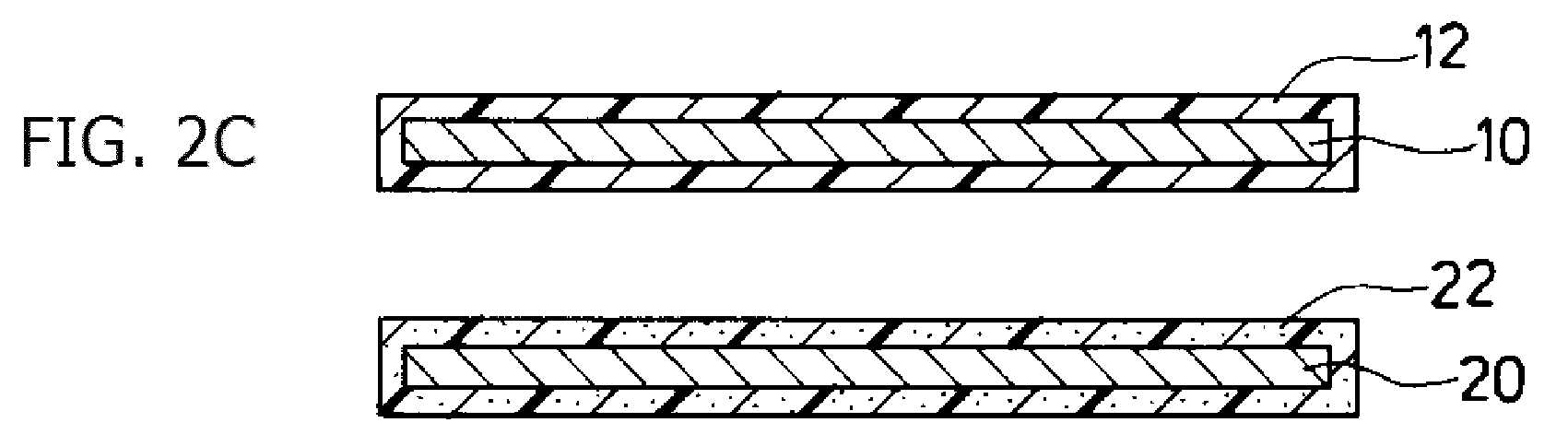
- the first bus bar 10 is subjected to a heating treatment at an appropriate temperature, so that the coating film 11 is dried by baking to form the completely-cured resin covering layer 12.
- the resin covering layer 12 having a predetermined and uniform thickness can be obtained. Even if the coating film 11 deposited on the surface of the first bus bar 10 has a pinhole, such a pinhole is compensated by its surrounding electrodeposition coating material during the heating treatment and thus filled up with the delayed arrival coating material. Thus, uniformity in the thickness of the resin covering layer 12 can be ensured.
- the second bus bar 20 is subjected to a heating treatment at an appropriate temperature, so that the coating film 21 is semi-cured to form the resin covering layer 22 in a soft state.
- the first bus bar 10 covered with the completely-cured resin covering layer 12 and the second bus bar 20 covered with the semi-cured resin covering layer 22 are overlapped with each other with the extended parts 10a and 20a being displaced relative to each other by a predetermined distance in the longitudinal direction.
- the first bus bar 10 and the second bus bar 20 are subjected to a heating treatment at an appropriate temperature while applying pressure thereto from the both sides thereof with an appropriate pressure. Consequently, the semi-cured resin covering layer 22 of the second bus bar 20 is cured again by being dried by baking with the thickness thereof being reduced by the application of pressure, thereby resulting in complete cure.
- the multi-layer bus bar unit 1 having the two-layer structure in which the first bus bar 10 and the second bus bar 20 are bonded to each other by the adhesion between the resin covering layers 12 and 22 is completed.
- the present inventors performed a confirmation test on adhesive strength of metal plates by resin covering layers using thermal shock test. Its test samples, test conditions, test direction, and test results will be described below.
- FIG. 3 As shown in FIG. 3 (FIG. 3(a) is a plan view, and FIG. 3 (b) is a side view), a first metal plate 70 having a thickness of 1.2 mm, a width of 20 mm, and a length of 100 mm and a second metal plate 71 having a thickness of 1.2 mm, a width of 10 mm, and a length of 100 mm were used as a test sample.
- the first metal plate 70 in which a coating film formed by an electrodeposition coating process using a polyamidimide resin solution was completely cured by a heating treatment and the second metal plate 71 in which a coating film similarly formed by the electrodeposition coating process using the polyamidimide resin solution was semi-cured by a heating treatment were overlapped with each other by 18 mm from the front edge of the second metal plate 71.
- the first metal plate 70 and the second metal plate 71 were subjected to a heating treatment while applying pressure thereto from the both sides thereof with an appropriate pressure. Consequently, the semi-cured resin covering layer of the second metal plate 71 was cured again, thereby resulting in complete cure. In this manner, the first metal plate 70 and the second metal plate 71 adhered to each other and thus integrated together via a resin covering layer 72 having a layer pressure of 0.1 mm (average).
- test samples 500 cycles, 1000 cycles, 2000 cycles, and 3000 cycles of thermal shock test, where one cycle (30 minutes) corresponds to -40°C/15 minutes and 165°C/15 minutes, were performed.
- test method was based on JIS K6850 [test method for tensile shear adhesive strength between adhesive and rigid adherend].
- the test rate was 0.3 mm/min.
- the test results show that an average tensile load of about 90 kgf and an average shear strength of about 5 MPa were maintained after the 3000 cycles of thermal shock test as compared to initial values (a tensile strength of about 200 kgf and a shear strength of about 11 MPa).
- the test sample has the average tensile strength after the 3000 cycles of thermal shock test of about 90 kgf and thus has a strength retention rate corresponding to about 45% of the initial value.
- the test sample has the average shear strength of about 5 MPa and thus has a strength retention rate also corresponding to about 45% of the initial value.
- a press die for punching a bus bar is generally only one component newly required for each demand for a multi-layer bus bar unit having different specifications such as a shape and dimensions.
- a press die for punching a bus bar is generally only one component newly required for each demand for a multi-layer bus bar unit having different specifications such as a shape and dimensions.
- production costs including initial introduction costs such as a cost for designing and manufacturing a die can be reduced.
- the resin covering layers for making the first bus bar and the second bus bar adhere to each other never experience, because of their production method, the occurrence of defects such as a weld line or a short, which may be generated in the injection molding. In addition, the occurrence of voids can be reduced sufficiently.
- a coating material having a high heat resistance property and a high mechanical strength such as polyimide, polyamide, epoxy, or preferably polyamidimide, is used in the electrodeposition coating. Consequently, the occurrence of defects such as separation caused by stress applied during use or thermal history can be reduced sufficiently, thereby ensuring long-term reliability including electrical and temporal reliability.
- FIG. 5 is a plan view
- FIG. 5 (b) is a cross-sectional view taken along line B-B in FIG. 5 (a) ) as a second embodiment
- an interval between a first bus bar 10 and a second bus bar 20 can be kept at an appropriate interval and uniformly by disposing space retention members 25 in an adhesion part between the first bus bar 10 covered with a resin covering layer 12 and the second bus bar 20 covered with a resin covering layer 22.
- two bus bars i.e., the first bus bar 10 formed from a metal flat plate machined to have a predetermined outline and dimensions and having masking applied to a pair of electrode terminal parts 10b and 10c and the second bus bar 20 formed from a metal flat plate machined to have a predetermined outline and dimensions and having masking applied to a pair of electrode terminal parts 20b and 20c, are prepared in advance.
- Coating films 11 and 21 are formed over the entire surface of the first bus bar 10 excluding the pair of electrode terminal parts 10b and 10c and the entire surface of the second bus bar 20 excluding the pair of electrode terminal parts 20b and 20c by the electrodeposition coating process (see FIG. 5 ).
- the coating films 11 and 21 of the first bus bar 10 and the second bus bar 20 are subjected to a heating treatment to form the semi-cured resin covering layers 12 and 22 as shown in FIG. 6(b) .
- the space retention members 25 formed from, for example, a plurality of glass beads or silica beads having a uniform diameter are disposed at substantially regular intervals between adhesion surfaces of the semi-cured resin covering layers 12 and 22 of the first bus bar 10 and the second bus bar 20 as shown in FIG. 6 (c) .
- the first bus bar 10 and the second bus bar 20 are overlapped with each other with the space retention members 25 being interposed therebetween.
- the first bus bar 10 and the second bus bar 20 are subjected to a heating treatment while applying pressure thereto from the both sides thereof with an appropriate pressure. Consequently, the semi-cured resin covering layers 12 and 22 of the first bus bar 10 and the second bus bar 20 are completely cured.
- a multi-layer bus bar unit 2 having a two-layer structure in which the first bus bar 10 and the second bus bar 20 with the interval therebetween being retained by the space retention members 25 are bonded to each other by the adhesion between the resin covering layers 12 and 22 is formed.
- the space retention members 25 With the use of the space retention members 25, a uniform interval between the bus bars can be reliably ensured even when the lengths of the bus bars are elongated. In addition, the interval between the bus bars can be easily set to a desired interval by appropriately selecting a size (diameter) of the space retention member 25. Even when the space retention members formed from a material of a different kind are included in the resin covering layers for making the bus bars adhere to each other as described above, the shear tensile strength can be kept at a practically problem-free level due to the large adhesion area of the elongated bus bars.
- a sheet material of the same kind as a resin material (electrodeposition coating material) for forming resin covering layers can be used as a space retention member in place of the above-described space retention members formed from glass or silica beads.
- a multi-layer bus bar unit 3 having a two-layer structure is formed, for example, by making a first bus bar 10 covered with a resin covering layer 12 formed from polyamidimide and a second bus bar 20 similarly covered with a resin covering layer 22 formed from polyamidimide adhere to each other via a space retention member 25 formed from a polyamidimide (PAI) sheet as shown in FIG. 7 (FIG. 7(a) is a plan view, and FIG. 7(b) is a cross-sectional view taken along line C-C in FIG. 7(a) ).
- PAI polyamidimide
- coating films are formed over the entire surface of the first bus bar 10 excluding a pair of electrode terminal parts 10b and 10c and the entire surface of the second bus bar 20 excluding a pair of electrode terminal parts 20b and 20c by the electrodeposition coating process. Thereafter, the coating films are subjected to a heating treatment at an appropriate temperature, so that the coating films are semi-cured to form the resin covering layers 12 and 22.
- the first bus bar 10 and the second bus bar 20 covered with the semi-cured resin covering layers 12 and 22, respectively, are overlapped with each other with the space retention member 25, formed from the PAI sheet, being interposed therebetween.
- the first bus bar 10 and the second bus bar 20 are subjected to a heating treatment at an appropriate temperature while applying pressure thereto from the both sides thereof with an appropriate pressure. Consequently, the semi-cured resin covering layers 12 and 22 are cured again by being dried by baking, thereby resulting in complete cure.
- the multi-layer bus bar unit 3 having the two-layer structure including the two bus bars bonded to each other by the adhesion between the first bus bar 10 covered with the resin covering layer 12 and the second bus bar 20 covered with the resin covering layer 22 via the space retention member 25 formed from the PAI sheet is completed.
- the multi-layer bus bar unit 3 that uses the PAI sheet as the space retention member 25 employs the sheet material of the same kind as the resin material (electrodeposition coating material) for forming the resin covering layers 12 and 22 to be adhesion layers.
- the resin material electrodeposition coating material
- FIG. 8 is a plan view
- FIG. 8(b) is a cross-sectional view taken along line D-D in FIG.
- a multi-layer bus bar unit 4 having, for example, a three-layer structure formed from three bus bars including a first bus bar 30 covered with a resin covering layer 32, a second bus bar 35 covered with a resin covering layer 37, and a third bus bar 40 covered with a resin covering layer 42 can be formed.
- the three bus bars i. e. , the first bus bar 30 formed from a metal flat plate machined to have a predetermined outline and dimensions and having masking applied to a pair of electrode terminal parts 30b and 30c, the second bus bar 35 formed from a metal flat plate machined to have a predetermined outline and dimensions and having masking applied to a pair of electrode terminal parts 35b and 35c, and the third bus bar 40 formed from a metal flat plate machined to have a predetermined outline and dimensions and having masking applied to a pair of electrode terminal parts 40b and 40c, are prepared in advance.
- Coating films 31, 36, and 41 are formed over the entire surface of the first bus bar 30 excluding the pair of electrode terminal parts 30b and 30c, the entire surface of the second bus bar 35 excluding the pair of electrode terminal parts 35b and 35c, and the entire surface of the third bus bar 40 excluding the pair of electrode terminal parts 40b and 40c by the electrodeposition coating process (see FIG. 8 ).
- the coating films 31 and 41 of the two bus bars, i.e., the first bus bar 30 and the third bus bar 40, among the three bus bars are subjected to a heating treatment to form the completely-cured resin covering layers 32 and 42 as shown in FIG. 9(b) .
- the coating film 36 of the second bus bar 35 is subjected to a heating treatment to form the semi-cured resin covering layer 37.
- the first bus bar 30 and the third bus bar 40 covered with the completely-cured resin covering layers 32 and 42, respectively, are overlapped with each other with the second bus bar 35 covered with the semi-cured resin covering layer 37 being interposed therebetween.
- These bus bars are subjected to a heating treatment while applying pressure thereto from the both sides thereof with an appropriate pressure. Consequently, the semi-cured resin covering layer 37 of the second bus bar 35 is completely cured.
- the multi-layer bus bar unit 4 having the three-layer structure including the three bus bars bonded to one another by the adhesion between the resin covering layers 32 and 37 of the first bus bar 30 and the second bus bar 35 and the adhesion between the resin covering layers 37 and 42 of the second bus bar 35 and the third bus bar 40 is formed.
- FIG. 10 (FIG. 10(a) is a plan view, and FIG. 10(b) is a cross-sectional view taken along line E-E in FIG. 10 (a) ) shows a fifth embodiment.
- a multi-layer bus bar unit 5 having a four-layer structure in which four bus bars, i.e., a first bus bar 50 covered with a resin covering layer 52 over the entire surface thereof excluding electrode terminal parts 50b and 50c, a second bus bar 55 covered with a resin covering layer 57 over the entire surface thereof excluding electrode terminal parts 55b and 55c, a third bus bar 60 covered with a resin covering layer 62 over the entire surface thereof excluding electrode terminal parts 60b and 60c, and a fourth bus bar 65 covered with a resin covering layer 67 over the entire surface thereof excluding electrode terminal parts 65b and 65c, are bonded to one another is formed.
- the electrode terminal part 50b of the first bus bar 50 at the bottom layer and the electrode terminal part 60b of the third bus bar 60 at the third layer from the bottom as well as the electrode terminal part 50c and the electrode terminal part 60c are connected to each other by swaging, for example.
- the electrode terminal part 55b of the second bus bar 55 at the second layer from the bottom and the electrode terminal part 65b of the fourth bus bar 65 at the top layer as well as the electrode terminal part 55c and the electrode terminal part 65c are connected to each other by swaging, for example.
- coating films are formed over the entire surface of the first bus bar 50 excluding the pair of electrode terminal parts 50b and 50c, the entire surface of the second bus bar 55 excluding the pair of electrode terminal parts 55b and 55c, the entire surface of the third bus bar 60 excluding the pair of electrode terminal parts 60b and 60c, and the entire surface of the fourth bus bar 65 excluding the pair of electrode terminal parts 65b and 65c by the electrodeposition coating process.
- the coating films formed on the bus bars positioned at every other layer, for example, the first bus bar 50 and the third bus bar 60, in the multi-layer bus bar unit 5 having the four-layer structure are subjected to a heating treatment to be completely cured.
- the coating films formed on the remaining second bus bar 55 and fourth bus bar 65 are subjected to a heating treatment to be semi-cured.
- the first bus bar 50 and the third bus bar 60 covered with the completely-cured resin covering layers 52 and 62 and the second bus bar 55 and the fourth bus bar 65 covered with the semi-cured resin covering layers 57 and 67 are overlapped alternately.
- These bus bars are subjected to a heating treatment at an appropriate temperature while applying pressure thereto from the both sides thereof with an appropriate pressure. Consequently, the semi-cured resin covering layers 57 and 67 are cured again by being dried by baking, thereby resulting in complete cure. In this manner, the multi-layer bus bar unit having the four-layer structure including the four bus bars is completed.
- the first bus bar 50 and the third bus bar 60 having the electrode terminal parts 50b and 60b joined together and the second bus bar 55 and the fourth bus bar 65 having the electrode terminal parts 55b and 65b joined together are layered alternately.
- capacitance between the joined electrode terminal parts 50b and 60b and the joined electrode terminal parts 55b and 65b can be increased.
- the adhesion area of each of the four bus bars equals an opposed area between bus bars 101 and 102 that constitute a conventional multi-layer bus bar assembly 100 shown in FIG.
- the multi-layer bus bar unit 5 of the present embodiment has capacitance about three times that of the conventional multi-layer bus bar assembly 100.
- the pressure and heating treatment is performed when at least one bus bar is in a semi-cured state having high viscosity.
- a bus bar is prone to generate air bubbles or entrain air bubbles. Therefore, the bonding step involving the application of pressure and heating is preferably performed in a vacuum or under reduced pressure environment to prevent the mixing-in of air bubbles, although the bonding step can be performed under atmospheric pressure environment depending on demanded specifications of a multi-layer bus bar unit.
- the pressure and heating treatment is performed with the completely-cured resin covering layer or the hard space retention member being positioned between the bus bars opposed to each other.
- the diameters of the air bubbles in the thickness direction of the bus bar can be kept smaller than or equal to the thickness of the resin covering layer that has been deformed thinly from the semi-cured state to the completely-cured state.
- the thickness accuracy between the bus bars can be kept at or above a certain level, and deterioration in pressure resistance by the resin covering layers can be reduced.
- the coating films are formed over the entire surfaces of the bus bars excluding the electrode terminal parts in the film coating step.
- the coating films may be formed over the entire surfaces of the bus bars in the film coating step, and the electrode terminal parts may be exposed in a post-treatment step after the fabrication of the multi-layer bus bar unit.
- a method for removing the resin covering films that cover the electrode terminal parts in the multi-layer bus bar unit by laser machining, for example, is conceivable.
- a bus bar module in which a bus bar and an external circuit are integrated together can be configured by providing an exposed part at an appropriate position in the bus bar covered with a resin covering layer by a masking treatment before the film coating step or laser machining after the fabrication and then joining the exposed part with an electrode part of the external circuit, such as a circuit board, by solder joint, for example.
- achievement in downsizing can be expected as compared to a case where the bus bar and the external circuit are prepared separately and then modularized.
- the production process is completed by the electrodeposition film coating step, the thermal curing step, and the bonding step.
- a press die for punching a bus bar is generally only one component newly required for each demand for a multi-layer bus bar unit having different specifications such as a shape and dimensions.
- production costs including initial introduction costs such as a cost for designing and manufacturing a die can be reduced. It is also possible to cope with small lot production easily.
- the resin covering layers for covering the bus bars and making the bus bars adhere to each other are formed by the electrodeposition coating process.
- defects such as a weld line or a short, which may be generated in the injection molding, never occur because of their production method.
- the occurrence of voids can be reduced sufficiently.
- a coating material having a high heat resistance property and a high mechanical strength such as polyimide, polyamide, epoxy, or preferably polyamidimide, is used in the electrodeposition coating. Consequently, the occurrence of defects such as separation caused by stress applied during use or thermal history can be reduced sufficiently, thereby ensuring long-term reliability including electrical and temporal reliability.
Landscapes
- Chemical & Material Sciences (AREA)
- Engineering & Computer Science (AREA)
- Chemical Kinetics & Catalysis (AREA)
- Electrochemistry (AREA)
- Materials Engineering (AREA)
- Metallurgy (AREA)
- Organic Chemistry (AREA)
- Manufacturing & Machinery (AREA)
- Connection Of Batteries Or Terminals (AREA)
- Organic Insulating Materials (AREA)
- Inverter Devices (AREA)
- Fuses (AREA)
Abstract


Description
- The present invention relates to a method for producing a multi-layer bus bar unit, and more particularly relates to a method for producing a multi-layer bus bar unit in which a plurality of metal bodies (electric conductors) running parallel to each other are covered with resin covering layers.
- An example of a conventional multi-layer bus bar unit of this type is shown in
Patent Literature 1 disclosed under the title of "MULTI-LAYER BUS BAR ASSEMBLY AND MOLDING DEVICE FOR THE SAME." - As shown in
FIG. 11 , a disclosed multi-layerbus bar assembly 100 includes: flat plate-shaped conductors (bus bars) 101 and 102 running parallel to each other face-to-face; and a resin moldedpart 103 that fills a gap between thebus bars respective bus bars - Patent Literature 1: Japanese Patent Application Laid-Open No:
2007-215340 - By the way, to cover the
bus bars part 103 in the multi-layerbus bar assembly 100 having the above-described configuration, thebus bars part 103. Thus, every time a multi-layer bus bar unit having different specifications such as a shape and dimensions is demanded, a new mold needs to be designed and manufactured. Therefore, it may take time from the designing to launching of a product, thereby missing the timing to commercialize the product. Moreover, initial introduction costs including a cost for designing and manufacturing the mold are increased, thus leading to increase in the production costs. - If an interval between the
bus bars bus bar assembly 100 and increase capacitance between thebus bars bus bars bus bars - Due to the stress applied by operations such as assembling and wiring when the multi-layer
bus bar assembly 100 is mounted to a device or thermal history during long-term use, separation may occur between thebus bars part 103, thus deteriorating reliability for long-term use. - The present invention has been made in view of the above-described problems and it is an object of the present invention to provide a multi-layer bus bar unit capable of: easily coping with a demand for a multi-layer bus bar assembly (referred to as a "multi-layer bus bar unit" in the present invention) having different specifications such as a shape and dimensions; reducing an amount of time required before launching a product; reducing production costs including initial introduction costs such as a cost for designing and manufacturing a die; and ensuring long-term reliability including electrical and temporal reliability.
- To solve the above problems, an invention as set forth in
claim 1 of the present invention provides a method for producing a multi-layer bus bar unit having a multi-layer structure including a plurality of bus bars. The method includes the steps of: preparing a plurality of metal flat plate-shaped bus bars each having electrode terminal parts at two or more locations; depositing a coating film over an entire surface of each of the plurality of bus bars by electrodeposition coating with an electrodeposition coating material having heat resistance and insulation properties; subjecting a coating film of a predetermined bus bar among the plurality of bus bars with the coating films to a heating treatment, so that the coating film of the predetermined bus bar is completely cured; subjecting a bus bar other than the predetermined bus bar among the plurality of bus bars with the coating films to a heat treatment so that the bus bar other than the predetermined bus bar is semi-cured; and obtaining the multi-layer structure by alternately overlapping, and then subjecting to a pressure and heating treatment, the bus bar having the completely-cured coating film and the bus bar having the semi-cured coating film, so that the semi-cured coating film is completely cured and the plurality of bus bars adhere to each other by the completely-cured coating film. - An invention as set forth in
claim 2 of the present invention is characterized in that the electrodeposition coating material inclaim 1 is any of polyimide, polyamide, epoxy, and polyamidimide. - An invention as set forth in
claim 3 of the present invention is characterized in that a step of applying masking to the electrode terminal parts of each of the plurality of bus bars is provided before the step of depositing the coating films, and a step of removing the masking and thereby exposing the electrode terminal parts is provided after the step of obtaining the multi-layer structure in any ofclaim 1 orclaim 2. - An invention as set forth in claim 4 of the present invention is characterized in that a step of removing the completely-cured coating films covering the electrode terminal parts and thereby exposing the electrode terminal parts is provided after the step of obtaining the multi-layer structure in any of
claim 1 orclaim 2. - An invention as set forth in
claim 5 of the present invention provides a method for producing a multi-layer bus bar unit having a multi-layer structure including a plurality of bus bars. The method includes the steps of: preparing a plurality of metal flat plate-shaped bus bars each having electrode terminal parts at two or more locations; depositing a coating film over an entire surface of each of the plurality of bus bars by electrodeposition coating with an electrodeposition coating material having heat resistance and insulation properties; subjecting the plurality of bus bars with the coating films to a heating treatment, so that the plurality of bus bars are semi-cured; and obtaining the multi-layer structure by overlapping, and then subjecting to a pressure and heating treatment, the bus bars having the semi-cured coating films with a space retention member being interposed therebetween, so that the semi-cured coating films are completely cured and the plurality of bus bars adhere to each other by the completely-cured coating films. - An invention as set forth in claim 6 of the present invention is characterized in that the electrodeposition coating material in
claim 5 is any of polyimide, polyamide, epoxy, and polyamidimide. - An invention as set forth in claim 7 of the present invention is characterized in that the space retention member in any of
claim 5 or claim 6 is any of a glass bead, a silica bead, and a sheet material of the same kind as the electrodeposition coating material. - An invention as set forth in claim 8 of the present invention is characterized in that a step of applying masking to the electrode terminal parts of each of the plurality of bus bars is provided before the step of depositing the coating films, and a step of removing the masking and thereby exposing the electrode terminal parts is provided after the step of obtaining the multi-layer structure in any one of
claims 5 to 7. - An invention as set forth in claim 9 of the present invention is characterized in that a step of removing the completely-cured coating films covering the electrode terminal parts and thereby exposing the electrode terminal parts is provided after the step of obtaining the multi-layer structure in any one of
claims 5 to 7. - According to the present invention, the coating film of the predetermined bus bar among the plurality of bus bars with the coating films formed by electrodeposition coating is completely cured, and the coating film of the bus bar other than the predetermined bus bar is semi-cured. The bus bar having the completely-cured coating film and the bus bar having the semi-cured coating film are overlapped alternately, and the semi-cured coating film is completely cured. In this manner, the multi-layer bus bar unit having the multi-layer structure in which the plurality of bus bars adhere to each other by the completely-cured coating film is fabricated.
- Accordingly, a press die for punching a bus bar is generally only one component newly required to commercialize a product coping with a demand for different specifications. Thus, it is possible to cope with a new product easily, and an amount of time required before launching the product can be reduced. Additionally, as compared to a case where an injection mold is used, production costs including initial costs such as a cost for manufacturing a die can be reduced.
- Moreover, the coating films never experience, because of their production method, the occurrence of defects such as a weld line or a short, which may be generated in the injection molding. In addition, the occurrence of voids can be reduced sufficiently.
- Furthermore, a coating material having a high heat resistance property and a high mechanical strength, such as polyimide, polyamide, epoxy, or preferably polyamidimide, is used in the electrodeposition coating. Consequently, the occurrence of defects such as separation caused by stress applied during use or thermal history can be reduced sufficiently, thereby ensuring long-term reliability including electrical and temporal reliability.
-
-
FIG. 1 is an explanatory diagram showing a multi-layer bus bar unit of a first embodiment. -
FIG. 2 is an explanatory diagram showing a production process of the multi-layer bus bar unit of the first embodiment. -
FIG. 3 is an explanatory diagram showing a test sample for thermal shock test. -
FIG. 4 is a table showing test results of thermal shock test. -
FIG. 5 is an explanatory diagram showing a multi-layer bus bar unit of a second embodiment. -
FIG. 6 is an explanatory diagram showing a production process of the multi-layer bus bar unit of the second embodiment. -
FIG. 7 is an explanatory diagram showing a multi-layer bus bar unit of a third embodiment. -
FIG. 8 is an explanatory diagram showing a multi-layer bus bar unit of a fourth embodiment. -
FIG. 9 is an explanatory diagram showing a production process of the multi-layer bus bar unit of the fourth embodiment. -
FIG. 10 is an explanatory diagram showing a multi-layer bus bar unit of a fifth embodiment. -
FIG. 11 is an explanatory diagram showing a conventional example. - Hereinafter, preferred embodiments of the present invention will be described in detail with reference to
FIGS. 1 to 10 (identical parts will be denoted by the same reference numerals). The embodiments to be described below are preferred specific examples of the present invention, and thus include technically-preferred various limitations. The scope of the present invention, however, is not limited to these embodiments unless explicitly stated in the following description that the present invention is limited thereby. -
FIG. 1 is an explanatory diagram showing a multi-layer bus bar unit of a first embodiment according to the present invention.FIG. 1(a) is a plan view, andFIG. 1(b) is a cross-sectional view taken along line A-A inFIG. 1(a) . - In a multi-layer
bus bar unit 1 of the present embodiment, two bus bars, i.e., afirst bus bar 10 and asecond bus bar 20 each formed from a metal member, are covered withresin covering layers bus bars resin covering layers bus bar unit 1 having a two-layer structure. - The
first bus bar 10 constituting the multi-layerbus bar unit 1 has: anextended part 10a having a long plate shape; and a pair ofelectrode terminal parts extended part 10a. Similarly, thesecond bus bar 20 constituting the multi-layerbus bar unit 1 has: anextended part 20a having a long plate shape; and a pair ofelectrode terminal parts extended part 20a. - The
extended part 10a of thefirst bus bar 10 and theextended part 20a of thesecond bus bar 20 each function as a current path (power path). Among the pair ofelectrode terminal parts first bus bar 10 and theelectrode terminal parts second bus bar 20, one set of theelectrode terminal parts electrode terminal parts first bus bar 10 and thesecond bus bar 20 to the external device. - In other words, the
first bus bar 10 and thesecond bus bar 20 have substantially the same outline and dimensions, and have a positional relationship in which thefirst bus bar 10 and thesecond bus bar 20 are disposed face-to-face while being displaced relative to each other in a longitudinal direction thereof. - The
first bus bar 10 and thesecond bus bar 20 run parallel to each other with the extendedparts first bus bar 10 and thesecond bus bar 20 are covered with theresin covering layers electrode terminal parts first bus bar 10 and the pair ofelectrode terminal parts second bus bar 20. At the same time, the gap between theextended parts resin covering layers extended parts resin covering layers - A method for producing the multi-layer bus bar unit having the above-described configuration will be described next with reference to
FIG. 2 . - First, in a step of preparing bus bars shown in
FIG. 2 (a) , two bus bars, i.e., the flat plate-shapedfirst bus bar 10 andsecond bus bar 20 formed from metal members machined to have predetermined substantially the same outline and dimensions by means of punching with a punching press die, for example, are prepared. - The
first bus bar 10 constituting the multi-layerbus bar unit 1 has: theextended part 10a having a long plate shape; and the pair ofelectrode terminal parts extended part 10a. Thesecond bus bar 20 constituting the multi-layerbus bar unit 1 has: theextended part 20a having a long plate shape; and the pair ofelectrode terminal parts extended part 20a (seeFIG. 1 ). - Next, in a film coating step in
FIG. 2(b) , masking is applied in advance to each of the pair ofelectrode terminal parts first bus bar 10 and the pair ofelectrode terminal parts second bus bar 20.Coating films first bus bar 10 excluding the pair ofelectrode terminal parts second bus bar 20 excluding the pair ofelectrode terminal parts - The
coating film 11 of thefirst bus bar 10 and thecoating film 21 of thesecond bus bar 20 are each formed by surface deposition by a conventional electrodeposition coating process with an electrodeposition coating material by a solution of a resin, such as polyimide, polyamide, epoxy, or preferably polyamidimide having excellent heat resistance and insulation properties. - Next, in a step of thermal curing the coating films in
FIG. 2(c) , thefirst bus bar 10 is subjected to a heating treatment at an appropriate temperature, so that thecoating film 11 is dried by baking to form the completely-curedresin covering layer 12. In this manner, theresin covering layer 12 having a predetermined and uniform thickness can be obtained. Even if thecoating film 11 deposited on the surface of thefirst bus bar 10 has a pinhole, such a pinhole is compensated by its surrounding electrodeposition coating material during the heating treatment and thus filled up with the delayed arrival coating material. Thus, uniformity in the thickness of theresin covering layer 12 can be ensured. - The
second bus bar 20, on the other hand, is subjected to a heating treatment at an appropriate temperature, so that thecoating film 21 is semi-cured to form theresin covering layer 22 in a soft state. - Finally, in a bonding step in
FIG. 2(d) , thefirst bus bar 10 covered with the completely-curedresin covering layer 12 and thesecond bus bar 20 covered with the semi-curedresin covering layer 22 are overlapped with each other with theextended parts first bus bar 10 and thesecond bus bar 20 are subjected to a heating treatment at an appropriate temperature while applying pressure thereto from the both sides thereof with an appropriate pressure. Consequently, the semi-curedresin covering layer 22 of thesecond bus bar 20 is cured again by being dried by baking with the thickness thereof being reduced by the application of pressure, thereby resulting in complete cure. In this manner, the multi-layerbus bar unit 1 having the two-layer structure in which thefirst bus bar 10 and thesecond bus bar 20 are bonded to each other by the adhesion between theresin covering layers - For the large-scale production of such a multi-layer bus bar unit, continuously-connected multi-layer bus bar units are introduced into the production process. Accordingly, a dicing step of cutting the continuously-connected multi-layer bus bar units at predetermined dicing positions for singulation into individual multi-layer bus bar units is provided after the bonding step, although such a step is not shown in the figures.
- The present inventors performed a confirmation test on adhesive strength of metal plates by resin covering layers using thermal shock test. Its test samples, test conditions, test direction, and test results will be described below.
- As shown in
FIG. 3 (FIG. 3(a) is a plan view, andFIG. 3 (b) is a side view), afirst metal plate 70 having a thickness of 1.2 mm, a width of 20 mm, and a length of 100 mm and asecond metal plate 71 having a thickness of 1.2 mm, a width of 10 mm, and a length of 100 mm were used as a test sample. Thefirst metal plate 70 in which a coating film formed by an electrodeposition coating process using a polyamidimide resin solution was completely cured by a heating treatment and thesecond metal plate 71 in which a coating film similarly formed by the electrodeposition coating process using the polyamidimide resin solution was semi-cured by a heating treatment were overlapped with each other by 18 mm from the front edge of thesecond metal plate 71. Thefirst metal plate 70 and thesecond metal plate 71 were subjected to a heating treatment while applying pressure thereto from the both sides thereof with an appropriate pressure. Consequently, the semi-cured resin covering layer of thesecond metal plate 71 was cured again, thereby resulting in complete cure. In this manner, thefirst metal plate 70 and thesecond metal plate 71 adhered to each other and thus integrated together via aresin covering layer 72 having a layer pressure of 0.1 mm (average). - As to the test conditions, 500 cycles, 1000 cycles, 2000 cycles, and 3000 cycles of thermal shock test, where one cycle (30 minutes) corresponds to -40°C/15 minutes and 165°C/15 minutes, were performed. The number (n) of the test samples was n = 3 for each thermal shock cycle number.
- The test method was based on JIS K6850 [test method for tensile shear adhesive strength between adhesive and rigid adherend]. The test rate was 0.3 mm/min.
- As shown in a table in
FIG. 4 , despite of being exposed to severe thermal shock test with a temperature variation range of 200°C or more, the test results show that an average tensile load of about 90 kgf and an average shear strength of about 5 MPa were maintained after the 3000 cycles of thermal shock test as compared to initial values (a tensile strength of about 200 kgf and a shear strength of about 11 MPa). In other words, the test sample has the average tensile strength after the 3000 cycles of thermal shock test of about 90 kgf and thus has a strength retention rate corresponding to about 45% of the initial value. Further, the test sample has the average shear strength of about 5 MPa and thus has a strength retention rate also corresponding to about 45% of the initial value. - Although a high-temperature heating test for 300°C/five minutes was performed in addition to the aforementioned adhesive strength test, no separation between
metal plates 55 and 56 was observed. - By producing a multi-layer bus bar unit by the above-described production method, the electrodeposition film coating step, the thermal curing step, and the bonding step complete the production process. Thus, a press die for punching a bus bar is generally only one component newly required for each demand for a multi-layer bus bar unit having different specifications such as a shape and dimensions. Thus, it is possible to cope with demanded specifications of a multi-layer bus bar unit easily, and an amount of time required before launching a product can be reduced. Additionally, as compared to a case where an injection mold is used, production costs including initial introduction costs such as a cost for designing and manufacturing a die can be reduced.
- Moreover, the resin covering layers for making the first bus bar and the second bus bar adhere to each other never experience, because of their production method, the occurrence of defects such as a weld line or a short, which may be generated in the injection molding. In addition, the occurrence of voids can be reduced sufficiently.
- Furthermore, a coating material having a high heat resistance property and a high mechanical strength, such as polyimide, polyamide, epoxy, or preferably polyamidimide, is used in the electrodeposition coating. Consequently, the occurrence of defects such as separation caused by stress applied during use or thermal history can be reduced sufficiently, thereby ensuring long-term reliability including electrical and temporal reliability.
- As shown in
FIG. 5 (FIG. 5(a) is a plan view, andFIG. 5 (b) is a cross-sectional view taken along line B-B inFIG. 5 (a) ) as a second embodiment, an interval between afirst bus bar 10 and asecond bus bar 20 can be kept at an appropriate interval and uniformly by disposingspace retention members 25 in an adhesion part between thefirst bus bar 10 covered with aresin covering layer 12 and thesecond bus bar 20 covered with aresin covering layer 22. - Specifically, as shown in
FIG. 6 (a) , two bus bars, i.e., thefirst bus bar 10 formed from a metal flat plate machined to have a predetermined outline and dimensions and having masking applied to a pair ofelectrode terminal parts second bus bar 20 formed from a metal flat plate machined to have a predetermined outline and dimensions and having masking applied to a pair ofelectrode terminal parts Coating films first bus bar 10 excluding the pair ofelectrode terminal parts second bus bar 20 excluding the pair ofelectrode terminal parts FIG. 5 ). - Next, the coating
films first bus bar 10 and thesecond bus bar 20 are subjected to a heating treatment to form the semi-curedresin covering layers FIG. 6(b) . - Finally, the
space retention members 25 formed from, for example, a plurality of glass beads or silica beads having a uniform diameter are disposed at substantially regular intervals between adhesion surfaces of the semi-curedresin covering layers first bus bar 10 and thesecond bus bar 20 as shown inFIG. 6 (c) . Thefirst bus bar 10 and thesecond bus bar 20 are overlapped with each other with thespace retention members 25 being interposed therebetween. Thefirst bus bar 10 and thesecond bus bar 20 are subjected to a heating treatment while applying pressure thereto from the both sides thereof with an appropriate pressure. Consequently, the semi-curedresin covering layers first bus bar 10 and thesecond bus bar 20 are completely cured. In this manner, a multi-layerbus bar unit 2 having a two-layer structure in which thefirst bus bar 10 and thesecond bus bar 20 with the interval therebetween being retained by thespace retention members 25 are bonded to each other by the adhesion between theresin covering layers - With the use of the
space retention members 25, a uniform interval between the bus bars can be reliably ensured even when the lengths of the bus bars are elongated. In addition, the interval between the bus bars can be easily set to a desired interval by appropriately selecting a size (diameter) of thespace retention member 25. Even when the space retention members formed from a material of a different kind are included in the resin covering layers for making the bus bars adhere to each other as described above, the shear tensile strength can be kept at a practically problem-free level due to the large adhesion area of the elongated bus bars. - As a third embodiment, a sheet material of the same kind as a resin material (electrodeposition coating material) for forming resin covering layers can be used as a space retention member in place of the above-described space retention members formed from glass or silica beads. Specifically, a multi-layer
bus bar unit 3 having a two-layer structure is formed, for example, by making afirst bus bar 10 covered with aresin covering layer 12 formed from polyamidimide and asecond bus bar 20 similarly covered with aresin covering layer 22 formed from polyamidimide adhere to each other via aspace retention member 25 formed from a polyamidimide (PAI) sheet as shown inFIG. 7 (FIG. 7(a) is a plan view, andFIG. 7(b) is a cross-sectional view taken along line C-C inFIG. 7(a) ). - Although a production process of the multi-layer
bus bar unit 3 according to the present embodiment is not shown in the figures, coating films are formed over the entire surface of thefirst bus bar 10 excluding a pair ofelectrode terminal parts second bus bar 20 excluding a pair ofelectrode terminal parts resin covering layers first bus bar 10 and thesecond bus bar 20 covered with the semi-curedresin covering layers space retention member 25, formed from the PAI sheet, being interposed therebetween. Thefirst bus bar 10 and thesecond bus bar 20 are subjected to a heating treatment at an appropriate temperature while applying pressure thereto from the both sides thereof with an appropriate pressure. Consequently, the semi-curedresin covering layers bus bar unit 3 having the two-layer structure including the two bus bars bonded to each other by the adhesion between thefirst bus bar 10 covered with theresin covering layer 12 and thesecond bus bar 20 covered with theresin covering layer 22 via thespace retention member 25 formed from the PAI sheet is completed. - The multi-layer
bus bar unit 3 that uses the PAI sheet as thespace retention member 25 employs the sheet material of the same kind as the resin material (electrodeposition coating material) for forming theresin covering layers - Although the multi-layer
bus bar units first bus bar 10 and thesecond bus bar 20 have been described in the first to third embodiments described above, a multi-layer bus bar unit is not necessarily limited to the two-layer structure. As a fourth embodiment (seeFIG. 8 (FIG. 8(a) is a plan view, andFIG. 8(b) is a cross-sectional view taken along line D-D inFIG. 8 (a) )), a multi-layer bus bar unit 4 having, for example, a three-layer structure formed from three bus bars including afirst bus bar 30 covered with aresin covering layer 32, asecond bus bar 35 covered with aresin covering layer 37, and athird bus bar 40 covered with aresin covering layer 42 can be formed. - In such a case, as shown in
FIG. 9 (a) , the three bus bars, i. e. , thefirst bus bar 30 formed from a metal flat plate machined to have a predetermined outline and dimensions and having masking applied to a pair ofelectrode terminal parts second bus bar 35 formed from a metal flat plate machined to have a predetermined outline and dimensions and having masking applied to a pair ofelectrode terminal parts third bus bar 40 formed from a metal flat plate machined to have a predetermined outline and dimensions and having masking applied to a pair ofelectrode terminal parts Coating films first bus bar 30 excluding the pair ofelectrode terminal parts second bus bar 35 excluding the pair ofelectrode terminal parts third bus bar 40 excluding the pair ofelectrode terminal parts FIG. 8 ). - Next, the coating
films 31 and 41 of the two bus bars, i.e., thefirst bus bar 30 and thethird bus bar 40, among the three bus bars are subjected to a heating treatment to form the completely-curedresin covering layers FIG. 9(b) . Thecoating film 36 of thesecond bus bar 35, on the other hand, is subjected to a heating treatment to form the semi-curedresin covering layer 37. - Finally, as shown in
FIG. 9 (c) , thefirst bus bar 30 and thethird bus bar 40 covered with the completely-curedresin covering layers second bus bar 35 covered with the semi-curedresin covering layer 37 being interposed therebetween. These bus bars are subjected to a heating treatment while applying pressure thereto from the both sides thereof with an appropriate pressure. Consequently, the semi-curedresin covering layer 37 of thesecond bus bar 35 is completely cured. In this manner, the multi-layer bus bar unit 4 having the three-layer structure including the three bus bars bonded to one another by the adhesion between theresin covering layers first bus bar 30 and thesecond bus bar 35 and the adhesion between theresin covering layers second bus bar 35 and thethird bus bar 40 is formed. -
FIG. 10 (FIG. 10(a) is a plan view, andFIG. 10(b) is a cross-sectional view taken along line E-E inFIG. 10 (a) ) shows a fifth embodiment. In the present embodiment, a multi-layerbus bar unit 5 having a four-layer structure in which four bus bars, i.e., afirst bus bar 50 covered with aresin covering layer 52 over the entire surface thereof excludingelectrode terminal parts second bus bar 55 covered with aresin covering layer 57 over the entire surface thereof excludingelectrode terminal parts third bus bar 60 covered with aresin covering layer 62 over the entire surface thereof excludingelectrode terminal parts fourth bus bar 65 covered with aresin covering layer 67 over the entire surface thereof excludingelectrode terminal parts - The
electrode terminal part 50b of thefirst bus bar 50 at the bottom layer and theelectrode terminal part 60b of thethird bus bar 60 at the third layer from the bottom as well as theelectrode terminal part 50c and theelectrode terminal part 60c are connected to each other by swaging, for example. Similarly, theelectrode terminal part 55b of thesecond bus bar 55 at the second layer from the bottom and theelectrode terminal part 65b of thefourth bus bar 65 at the top layer as well as theelectrode terminal part 55c and theelectrode terminal part 65c are connected to each other by swaging, for example. - Although a production process of the multi-layer
bus bar unit 5 according to the present embodiment is not shown in the figures, coating films are formed over the entire surface of thefirst bus bar 50 excluding the pair ofelectrode terminal parts second bus bar 55 excluding the pair ofelectrode terminal parts third bus bar 60 excluding the pair ofelectrode terminal parts fourth bus bar 65 excluding the pair ofelectrode terminal parts first bus bar 50 and thethird bus bar 60, in the multi-layerbus bar unit 5 having the four-layer structure are subjected to a heating treatment to be completely cured. The coating films formed on the remainingsecond bus bar 55 andfourth bus bar 65 are subjected to a heating treatment to be semi-cured. - Thereafter, the
first bus bar 50 and thethird bus bar 60 covered with the completely-curedresin covering layers second bus bar 55 and thefourth bus bar 65 covered with the semi-curedresin covering layers resin covering layers - In this case, the
first bus bar 50 and thethird bus bar 60 having theelectrode terminal parts second bus bar 55 and thefourth bus bar 65 having theelectrode terminal parts electrode terminal parts electrode terminal parts bus bars bus bar assembly 100 shown inFIG. 11 and an interval between two bus bars bonded to each other among the four bus bars equals an interval between the bus bars 101 and 102 that constitute the multi-layerbus bar assembly 100, the multi-layerbus bar unit 5 of the present embodiment has capacitance about three times that of the conventional multi-layerbus bar assembly 100. - In the first to fifth embodiments described above, the pressure and heating treatment is performed when at least one bus bar is in a semi-cured state having high viscosity. Thus, such a bus bar is prone to generate air bubbles or entrain air bubbles. Therefore, the bonding step involving the application of pressure and heating is preferably performed in a vacuum or under reduced pressure environment to prevent the mixing-in of air bubbles, although the bonding step can be performed under atmospheric pressure environment depending on demanded specifications of a multi-layer bus bar unit.
- However, suppose a case where by introducing a bus bar covered with a completely-cured resin covering layer or a hard space retention member into the bonding step, the pressure and heating treatment is performed with the completely-cured resin covering layer or the hard space retention member being positioned between the bus bars opposed to each other. In such a case, even when air bubbles are mixed in by performing the pressure and heating treatment under the atmospheric pressure environment, the diameters of the air bubbles in the thickness direction of the bus bar can be kept smaller than or equal to the thickness of the resin covering layer that has been deformed thinly from the semi-cured state to the completely-cured state. Thus, the thickness accuracy between the bus bars can be kept at or above a certain level, and deterioration in pressure resistance by the resin covering layers can be reduced.
- In the production processes of the multi-layer bus bar units described above, masking is applied to the electrode terminal parts before the film coating step of the coating films, so that the coating films are formed over the entire surfaces of the bus bars excluding the electrode terminal parts in the film coating step. However, the coating films may be formed over the entire surfaces of the bus bars in the film coating step, and the electrode terminal parts may be exposed in a post-treatment step after the fabrication of the multi-layer bus bar unit. Specifically, a method for removing the resin covering films that cover the electrode terminal parts in the multi-layer bus bar unit by laser machining, for example, is conceivable.
- Moreover, a bus bar module in which a bus bar and an external circuit are integrated together can be configured by providing an exposed part at an appropriate position in the bus bar covered with a resin covering layer by a masking treatment before the film coating step or laser machining after the fabrication and then joining the exposed part with an electrode part of the external circuit, such as a circuit board, by solder joint, for example. In this case, achievement in downsizing can be expected as compared to a case where the bus bar and the external circuit are prepared separately and then modularized.
- As described above, in the method for producing a multi-layer bus bar unit according to the present invention, the production process is completed by the electrodeposition film coating step, the thermal curing step, and the bonding step. Thus, a press die for punching a bus bar is generally only one component newly required for each demand for a multi-layer bus bar unit having different specifications such as a shape and dimensions. Thus, it is possible to cope with demanded specifications of a multi-layer bus bar unit easily, and an amount of time required before launching a product can be reduced. Additionally, as compared to a case where an injection mold is used, production costs including initial introduction costs such as a cost for designing and manufacturing a die can be reduced. It is also possible to cope with small lot production easily.
- Moreover, the resin covering layers for covering the bus bars and making the bus bars adhere to each other are formed by the electrodeposition coating process. Thus, defects such as a weld line or a short, which may be generated in the injection molding, never occur because of their production method. In addition, the occurrence of voids can be reduced sufficiently.
- Moreover, a coating material having a high heat resistance property and a high mechanical strength, such as polyimide, polyamide, epoxy, or preferably polyamidimide, is used in the electrodeposition coating. Consequently, the occurrence of defects such as separation caused by stress applied during use or thermal history can be reduced sufficiently, thereby ensuring long-term reliability including electrical and temporal reliability.
- Furthermore, when a plurality of bus bars, each formed from a metal flat plate, are multiply-disposed face-to-face via resin covering layers, the formation of the resin covering layers is performed by the step including the electrodeposition coating and the pressure and heating treatment. Thus, an interval between the bus bars disposed face-to-face can be made small, thereby increasing capacitance between the bus bars. Consequently, the use in a power line of a switching circuit, for example, enables the prevention of surge by fine decoupling effect due to the capacitance between the bus bars. Reference Signs List
-
- 1
- multi-layer bus bar unit
- 2
- multi-layer bus bar unit
- 3
- multi-layer bus bar unit
- 4
- multi-layer bus bar unit
- 5
- multi-layer bus bar unit
- 10
- first bus bar
- 10a
- extended part
- 10b
- electrode terminal part
- 10c
- electrode terminal part
- 11
- coating film
- 12
- resin covering layer
- 20
- second bus bar
- 20a
- extended part
- 20b
- electrode terminal part
- 20c
- electrode terminal part
- 21
- coating film
- 22
- resin covering layer
- 25
- space retention member
- 30
- first bus bar
- 30b
- electrode terminal part
- 30c
- electrode terminal part
- 31
- coating film
- 32
- resin covering layer
- 35
- second bus bar
- 35b
- electrode terminal part
- 35c
- electrode terminal part
- 36
- coating film
- 37
- resin covering layer
- 40
- third bus bar
- 40b
- electrode terminal part
- 40c
- electrode terminal part
- 41
- coating film
- 42
- resin covering layer
- 50
- first bus bar
- 50b
- electrode terminal part
- 50c
- electrode terminal part
- 52
- resin covering layer
- 55
- second bus bar
- 55b
- electrode terminal part
- 55c
- electrode terminal part
- 57
- resin covering layer
- 60
- third bus bar
- 60b
- electrode terminal part
- 60c
- electrode terminal part
- 62
- resin covering layer
- 65
- fourth bus bar
- 65b
- electrode terminal part
- 65c
- electrode terminal part
- 67
- resin covering layer
- 70
- first metal plate
- 71
- second metal plate
- 72
- resin covering layer
Claims (9)
- A method for producing a multi-layer bus bar unit having a multi-layer structure including a plurality of bus bars, the method comprising the steps of:preparing a plurality of metal flat plate-shaped bus bars each having electrode terminal parts at two or more locations;depositing a coating film over an entire surface of each of the plurality of bus bars by electrodeposition coating with an electrodeposition coating material having heat resistance and insulation properties;subjecting a coating film of a predetermined bus bar among the plurality of bus bars with the coating films to a heating treatment, so that the coating film of the predetermined bus bar is completely cured;subjecting a bus bar other than the predetermined bus bar among the plurality of bus bars with the coating films to a heat treatment so that the bus bar other than the predetermined bus bar is semi-cured; andobtaining the multi-layer structure by alternately overlapping, and then subjecting to a pressure and heating treatment, the bus bar having the completely-cured coating film and the bus bar having the semi-cured coating film, so that the semi-cured coating film is completely cured and the plurality of bus bars adhere to each other by the completely-cured coating film.
- The method for producing a multi-layer bus bar unit according to claim 1, wherein the electrodeposition coating material is any of polyimide, polyamide, epoxy, and polyamidimide.
- The method for producing a multi-layer bus bar unit according to claim 1 or 2, comprising:before the step of depositing the coating films, a step of applying masking to the electrode terminal parts of each of the plurality of bus bars, andafter the step of obtaining the multi-layer structure, a step of removing the masking and thereby exposing the electrode terminal parts.
- The method for producing a multi-layer bus bar unit according to claim 1 or 2, comprising:after the step of obtaining the multi-layer structure, a step of removing the completely-cured coating films covering the electrode terminal parts and thereby exposing the electrode terminal parts.
- A method for producing a multi-layer bus bar unit having a multi-layer structure including a plurality of bus bars, the method comprising the steps of:preparing a plurality of metal flat plate-shaped bus bars each having electrode terminal parts at two or more locations;depositing a coating film over an entire surface of each of the plurality of bus bars by electrodeposition coating with an electrodeposition coating material having heat resistance and insulation properties;subjecting the plurality of bus bars with the coating films to a heating treatment, so that the plurality of bus bars are semi-cured; andobtaining the multi-layer structure by overlapping, and then subjecting to a pressure and heating treatment, the bus bars having the semi-cured coating films with a space retention member being interposed therebetween, so that the semi-cured coating films are completely cured and the plurality of bus bars adhere to each other by the completely-cured coating films.
- The method for producing a multi-layer bus bar unit according to claim 5, wherein the electrodeposition coating material is any of polyimide, polyamide, epoxy, and polyamidimide.
- The method for producing a multi-layer bus bar unit according to claim 5 or 6, wherein the space retention member is any of a glass bead, a silica bead, and a sheet material of a same kind as the electrodeposition coating material.
- The method for producing a multi-layer bus bar unit according to any one of claims 5 to 7, comprising:before the step of depositing the coating films, a step of applying masking to the electrode terminal parts of each of the plurality of bus bars; andafter the step of obtaining the multi-layer structure, a step of removing the masking and thereby exposing the electrode terminal parts.
- The method for producing a multi-layer bus bar unit according to any one of claims 5 to 7, comprising:after the step of obtaining the multi-layer structure, a step of removing the completely-cured coating films covering the electrode terminal parts and thereby exposing the electrode terminal parts.
Applications Claiming Priority (2)
| Application Number | Priority Date | Filing Date | Title |
|---|---|---|---|
| JP2015100708A JP6487769B2 (en) | 2015-05-18 | 2015-05-18 | Manufacturing method of laminated busbar unit |
| PCT/JP2016/002379 WO2016185706A1 (en) | 2015-05-18 | 2016-05-16 | Method for manufacturing layered bus bar unit |
Publications (3)
| Publication Number | Publication Date |
|---|---|
| EP3300086A1 true EP3300086A1 (en) | 2018-03-28 |
| EP3300086A4 EP3300086A4 (en) | 2019-01-02 |
| EP3300086B1 EP3300086B1 (en) | 2020-07-01 |
Family
ID=57319859
Family Applications (1)
| Application Number | Title | Priority Date | Filing Date |
|---|---|---|---|
| EP16796102.8A Active EP3300086B1 (en) | 2015-05-18 | 2016-05-16 | Method for manufacturing layered bus bar unit |
Country Status (4)
| Country | Link |
|---|---|
| US (1) | US10907268B2 (en) |
| EP (1) | EP3300086B1 (en) |
| JP (1) | JP6487769B2 (en) |
| WO (1) | WO2016185706A1 (en) |
Cited By (2)
| Publication number | Priority date | Publication date | Assignee | Title |
|---|---|---|---|---|
| WO2020083530A1 (en) * | 2018-10-25 | 2020-04-30 | Eaton Intelligent Power Limited | Low inductance bus assembly and power converter apparatus including the same |
| GB2552057B (en) * | 2016-05-04 | 2021-09-01 | Fujitsu Ltd | Line, arrangement and server insert |
Families Citing this family (23)
| Publication number | Priority date | Publication date | Assignee | Title |
|---|---|---|---|---|
| JP6637002B2 (en) | 2017-09-04 | 2020-01-29 | サンコール株式会社 | Busbar assembly manufacturing method |
| JP6637003B2 (en) | 2017-09-08 | 2020-01-29 | サンコール株式会社 | Busbar assembly |
| JP6868198B2 (en) * | 2017-11-09 | 2021-05-12 | 日立金属株式会社 | Manufacturing method of insulated busbar and manufacturing method of laminated insulated busbar |
| JP7271130B2 (en) | 2018-10-23 | 2023-05-11 | サンコール株式会社 | busbar assembly |
| KR102041494B1 (en) * | 2019-01-22 | 2019-11-07 | 에스 티 (주) | Connecting busbar manufacturing method of battery for electric vehicle |
| US10741313B1 (en) * | 2019-02-06 | 2020-08-11 | Eaton Intelligent Power Limited | Bus bar assembly with integrated surge arrestor |
| JP7016836B2 (en) * | 2019-06-10 | 2022-02-07 | 矢崎総業株式会社 | Conductive system |
| JP7271333B2 (en) | 2019-06-25 | 2023-05-11 | サンコール株式会社 | Busbar assembly and manufacturing method thereof |
| JP6884835B2 (en) | 2019-09-27 | 2021-06-09 | サンコール株式会社 | Busbar assembly and its manufacturing method |
| KR102739498B1 (en) * | 2019-11-04 | 2024-12-06 | 주식회사 엘지에너지솔루션 | Flexible Busbar and Method Thereof |
| JP7123514B2 (en) * | 2020-06-17 | 2022-08-23 | 矢崎総業株式会社 | conductive structure |
| EP4170685A4 (en) | 2020-07-09 | 2024-03-13 | Suncall Corporation | BUS BAR ASSEMBLY AND ITS MANUFACTURING METHOD |
| US11551993B2 (en) | 2020-08-28 | 2023-01-10 | Ge Aviation Systems Llc | Power overlay module and method of assembling |
| RU2749558C1 (en) * | 2020-09-29 | 2021-06-15 | федеральное государственное бюджетное образовательное учреждение высшего образования «Томский государственный университет систем управления и радиоэлектроники» | Method for manufacturing power transmission line with spiral cross-section and device based on its basis |
| JP7569656B2 (en) | 2020-10-12 | 2024-10-18 | サンコール株式会社 | Manufacturing method of busbar assembly |
| JP7535918B2 (en) * | 2020-11-17 | 2024-08-19 | サンコール株式会社 | Busbar assembly and manufacturing method thereof |
| US11791597B2 (en) | 2021-02-05 | 2023-10-17 | Aptiv Technologies (2) S.À R.L. | Flexible electrical bus bar and method of manufacturing the same |
| JP7007512B1 (en) * | 2021-05-31 | 2022-02-10 | 株式会社アテックス | Conductive member and its manufacturing method |
| EP4187595A1 (en) * | 2021-11-29 | 2023-05-31 | Infineon Technologies AG | Terminal element or bus bar, and power semiconductor module arrangement comprising a terminal element or bus bar |
| US11832390B2 (en) | 2022-03-07 | 2023-11-28 | Rolls-Royce Corporation | Multilayer copper bus bars with soldered through hole components |
| US11876364B2 (en) | 2022-03-07 | 2024-01-16 | Rolls-Royce Corporation | Multilayer electronic components with soldered through holes |
| US20240429686A1 (en) * | 2023-06-20 | 2024-12-26 | Abb Schweiz Ag | Electrical busway assemblies and methods of assembling same |
| WO2026110374A1 (en) * | 2024-11-22 | 2026-05-28 | 三菱ケミカル株式会社 | Metal-resin joined body, flexible bus bar, and method for producing same |
Family Cites Families (23)
| Publication number | Priority date | Publication date | Assignee | Title |
|---|---|---|---|---|
| DE1515478B1 (en) * | 1965-05-18 | 1971-03-18 | Bbc Brown Boveri & Cie | Process for the production of a flat cable harness |
| US3345455A (en) * | 1965-11-15 | 1967-10-03 | Fed Pacific Electric Co | Insulated bus bar |
| US3662088A (en) * | 1970-01-20 | 1972-05-09 | Methode Mfg Corp | Electostatically coated laminated bus bar assembly |
| US3708609A (en) * | 1971-08-17 | 1973-01-02 | Rogers Corp | Laminated bus bar assembly |
| US4133101A (en) * | 1972-09-18 | 1979-01-09 | Amp Incorporated | Method of fabricating a laminated bus bar |
| JPS55160418A (en) * | 1979-05-31 | 1980-12-13 | Nippon Mektron Kk | Capacitor internally containing laminate bus and method of fabricating same |
| US4346257A (en) * | 1980-03-18 | 1982-08-24 | Eldre Components, Inc. | Laminated bus bar with dielectric ceramic inserts |
| US4430522A (en) * | 1982-07-16 | 1984-02-07 | Eldre Components, Inc. | Laminated bus bar with capacitors and method of making same |
| US4517406A (en) * | 1984-05-14 | 1985-05-14 | Eldre Components, Inc. | Laminated bus bar containing multilayer ceramic capacitors |
| US4867696A (en) * | 1988-07-15 | 1989-09-19 | Amp Incorporated | Laminated bus bar with power tabs |
| CN1268048C (en) | 2000-10-26 | 2006-08-02 | 铁道部株洲电力机车研究所 | Design and manufacture of low-inductance bus |
| DE10113258A1 (en) * | 2001-03-16 | 2002-09-19 | Alstom Switzerland Ltd | Manufacturing conducting rods involves insulating of coating sub-conductors, sintering, partial hardening of coating, assembly to form rod, sintering with compression and final hardening |
| JP4321001B2 (en) * | 2002-02-08 | 2009-08-26 | 日産自動車株式会社 | Painting method |
| US7557298B2 (en) * | 2002-10-14 | 2009-07-07 | World Properties, Inc. | Laminated bus bar assembly |
| JP2005251673A (en) * | 2004-03-08 | 2005-09-15 | Toyota Motor Corp | Bus bar manufacturing method, bus bar |
| JP4791713B2 (en) * | 2004-07-08 | 2011-10-12 | 株式会社協豊製作所 | Energizer |
| JP4815935B2 (en) | 2005-08-02 | 2011-11-16 | 日立電線株式会社 | Method for producing molded body |
| JP4822854B2 (en) | 2006-01-18 | 2011-11-24 | 株式会社有沢製作所 | Polyamideimide resin for flexible printed wiring board, metal-clad laminate, coverlay, flexible printed wiring board, and resin composition using the resin |
| JP4432913B2 (en) | 2006-02-10 | 2010-03-17 | 株式会社デンソー | Laminated bus bar assembly and molding apparatus therefor |
| JP5609298B2 (en) * | 2010-06-18 | 2014-10-22 | 富士電機株式会社 | Laminated busbar |
| GB2502926B (en) * | 2011-03-31 | 2014-11-26 | Eldre Corp | Multiple wrapped laminated bus bar system and method |
| US20170103831A1 (en) * | 2015-10-13 | 2017-04-13 | Littelfuse, Inc. | Methods for Manufacturing an Insulated Busbar |
| JP2018181780A (en) * | 2017-04-21 | 2018-11-15 | 矢崎総業株式会社 | Stacked bus bars and battery modules |
-
2015
- 2015-05-18 JP JP2015100708A patent/JP6487769B2/en active Active
-
2016
- 2016-05-16 US US15/575,208 patent/US10907268B2/en active Active
- 2016-05-16 WO PCT/JP2016/002379 patent/WO2016185706A1/en not_active Ceased
- 2016-05-16 EP EP16796102.8A patent/EP3300086B1/en active Active
Cited By (2)
| Publication number | Priority date | Publication date | Assignee | Title |
|---|---|---|---|---|
| GB2552057B (en) * | 2016-05-04 | 2021-09-01 | Fujitsu Ltd | Line, arrangement and server insert |
| WO2020083530A1 (en) * | 2018-10-25 | 2020-04-30 | Eaton Intelligent Power Limited | Low inductance bus assembly and power converter apparatus including the same |
Also Published As
| Publication number | Publication date |
|---|---|
| EP3300086B1 (en) | 2020-07-01 |
| JP6487769B2 (en) | 2019-03-20 |
| WO2016185706A1 (en) | 2016-11-24 |
| JP2016216766A (en) | 2016-12-22 |
| US20180148855A1 (en) | 2018-05-31 |
| EP3300086A4 (en) | 2019-01-02 |
| US10907268B2 (en) | 2021-02-02 |
Similar Documents
| Publication | Publication Date | Title |
|---|---|---|
| US10907268B2 (en) | Method for producing multi-layer bus bar unit | |
| US10910296B2 (en) | Lead frame and method of fabricating the same | |
| US10988418B2 (en) | Copper-ceramic substrate, copper precursor for producing a copper-ceramic substrate and process for producing a copper-ceramic substrate | |
| CN105103665B (en) | The manufacture method of resin multilayer substrate | |
| JP2007038490A (en) | Molded product and method for producing the same | |
| CN107211527A (en) | Semi-flexible printed circuit board (PCB) with embedded components | |
| TWI671829B (en) | Manufacturing method of semiconductor device | |
| CN107591421B (en) | Camera module chip packaging base assembly and preparation method thereof | |
| CN115923158B (en) | Method for manufacturing bonded component | |
| US10123413B2 (en) | Package substrate and manufacturing method thereof | |
| US7685707B2 (en) | Method for manufacturing circuit forming substrate | |
| US9178093B2 (en) | Solar cell module on molded lead-frame and method of manufacture | |
| US10729013B2 (en) | Semi-finished product for the production of connection systems for electronic components and method | |
| CN109411453B (en) | Vertical interconnection method for three-dimensional packaging | |
| CN110225678B (en) | Circuit board pressing method and prefabricated substrate | |
| KR101501407B1 (en) | Mica heater and production method thereof | |
| US20200305279A1 (en) | Semi-finished product for the production of connection systems for electronic components | |
| JP4053047B2 (en) | Manufacturing method of semiconductor device | |
| CN111696928B (en) | Semiconductor package structure and manufacturing method thereof | |
| CN103037638A (en) | Press fit method for to-be-pressed multi-layer plate with chip window | |
| CN109411366B (en) | A three-dimensional packaging method for surface protection | |
| KR20250033964A (en) | Method for manufacturing a fan-out package | |
| JP5709732B2 (en) | Manufacturing method of ceramic multilayer substrate | |
| JP2003338686A (en) | Method for manufacturing printed wiring board | |
| JP2019075428A (en) | Resin-sealed mold and resin sealing method |
Legal Events
| Date | Code | Title | Description |
|---|---|---|---|
| STAA | Information on the status of an ep patent application or granted ep patent |
Free format text: STATUS: THE INTERNATIONAL PUBLICATION HAS BEEN MADE |
|
| PUAI | Public reference made under article 153(3) epc to a published international application that has entered the european phase |
Free format text: ORIGINAL CODE: 0009012 |
|
| STAA | Information on the status of an ep patent application or granted ep patent |
Free format text: STATUS: REQUEST FOR EXAMINATION WAS MADE |
|
| 17P | Request for examination filed |
Effective date: 20171116 |
|
| AK | Designated contracting states |
Kind code of ref document: A1 Designated state(s): AL AT BE BG CH CY CZ DE DK EE ES FI FR GB GR HR HU IE IS IT LI LT LU LV MC MK MT NL NO PL PT RO RS SE SI SK SM TR |
|
| AX | Request for extension of the european patent |
Extension state: BA ME |
|
| DAV | Request for validation of the european patent (deleted) | ||
| DAX | Request for extension of the european patent (deleted) | ||
| RIC1 | Information provided on ipc code assigned before grant |
Ipc: C25D 13/00 20060101ALI20181119BHEP Ipc: B32B 15/08 20060101ALI20181119BHEP Ipc: C09D 5/44 20060101ALI20181119BHEP Ipc: C25D 13/06 20060101ALI20181119BHEP Ipc: H02G 5/00 20060101ALI20181119BHEP Ipc: H01B 13/00 20060101AFI20181119BHEP Ipc: H01B 3/40 20060101ALI20181119BHEP Ipc: C25D 13/12 20060101ALI20181119BHEP Ipc: H01B 3/30 20060101ALI20181119BHEP Ipc: C25D 13/22 20060101ALI20181119BHEP |
|
| A4 | Supplementary search report drawn up and despatched |
Effective date: 20181130 |
|
| STAA | Information on the status of an ep patent application or granted ep patent |
Free format text: STATUS: EXAMINATION IS IN PROGRESS |
|
| 17Q | First examination report despatched |
Effective date: 20191008 |
|
| REG | Reference to a national code |
Ref country code: DE Ref legal event code: R079 Ref document number: 602016039204 Country of ref document: DE Free format text: PREVIOUS MAIN CLASS: H01B0013000000 Ipc: C25D0013120000 |
|
| GRAP | Despatch of communication of intention to grant a patent |
Free format text: ORIGINAL CODE: EPIDOSNIGR1 |
|
| STAA | Information on the status of an ep patent application or granted ep patent |
Free format text: STATUS: GRANT OF PATENT IS INTENDED |
|
| RIC1 | Information provided on ipc code assigned before grant |
Ipc: C25D 13/22 20060101ALI20200127BHEP Ipc: C25D 13/12 20060101AFI20200127BHEP |
|
| INTG | Intention to grant announced |
Effective date: 20200218 |
|
| GRAS | Grant fee paid |
Free format text: ORIGINAL CODE: EPIDOSNIGR3 |
|
| GRAA | (expected) grant |
Free format text: ORIGINAL CODE: 0009210 |
|
| STAA | Information on the status of an ep patent application or granted ep patent |
Free format text: STATUS: THE PATENT HAS BEEN GRANTED |
|
| AK | Designated contracting states |
Kind code of ref document: B1 Designated state(s): AL AT BE BG CH CY CZ DE DK EE ES FI FR GB GR HR HU IE IS IT LI LT LU LV MC MK MT NL NO PL PT RO RS SE SI SK SM TR |
|
| REG | Reference to a national code |
Ref country code: CH Ref legal event code: EP Ref country code: AT Ref legal event code: REF Ref document number: 1286265 Country of ref document: AT Kind code of ref document: T Effective date: 20200715 |
|
| REG | Reference to a national code |
Ref country code: IE Ref legal event code: FG4D |
|
| REG | Reference to a national code |
Ref country code: DE Ref legal event code: R096 Ref document number: 602016039204 Country of ref document: DE |
|
| REG | Reference to a national code |
Ref country code: DE Ref legal event code: R081 Ref document number: 602016039204 Country of ref document: DE Owner name: SUNCALL CORPORATION, KYOTO-SHI, JP Free format text: FORMER OWNER: SUNCALL CORP., KYOTO-SHI, JP Ref country code: DE Ref legal event code: R081 Ref document number: 602016039204 Country of ref document: DE Owner name: STANLEY ELECTRIC CO., LTD., JP Free format text: FORMER OWNER: SUNCALL CORP., KYOTO-SHI, JP Ref country code: DE Ref legal event code: R082 Ref document number: 602016039204 Country of ref document: DE Representative=s name: WAGNER & GEYER PARTNERSCHAFT MBB PATENT- UND R, DE |
|
| REG | Reference to a national code |
Ref country code: LT Ref legal event code: MG4D |
|
| PG25 | Lapsed in a contracting state [announced via postgrant information from national office to epo] |
Ref country code: BG Free format text: LAPSE BECAUSE OF FAILURE TO SUBMIT A TRANSLATION OF THE DESCRIPTION OR TO PAY THE FEE WITHIN THE PRESCRIBED TIME-LIMIT Effective date: 20201001 |
|
| REG | Reference to a national code |
Ref country code: NL Ref legal event code: MP Effective date: 20200701 |
|
| REG | Reference to a national code |
Ref country code: AT Ref legal event code: MK05 Ref document number: 1286265 Country of ref document: AT Kind code of ref document: T Effective date: 20200701 |
|
| PG25 | Lapsed in a contracting state [announced via postgrant information from national office to epo] |
Ref country code: GR Free format text: LAPSE BECAUSE OF FAILURE TO SUBMIT A TRANSLATION OF THE DESCRIPTION OR TO PAY THE FEE WITHIN THE PRESCRIBED TIME-LIMIT Effective date: 20201002 Ref country code: SE Free format text: LAPSE BECAUSE OF FAILURE TO SUBMIT A TRANSLATION OF THE DESCRIPTION OR TO PAY THE FEE WITHIN THE PRESCRIBED TIME-LIMIT Effective date: 20200701 Ref country code: NO Free format text: LAPSE BECAUSE OF FAILURE TO SUBMIT A TRANSLATION OF THE DESCRIPTION OR TO PAY THE FEE WITHIN THE PRESCRIBED TIME-LIMIT Effective date: 20201001 Ref country code: AT Free format text: LAPSE BECAUSE OF FAILURE TO SUBMIT A TRANSLATION OF THE DESCRIPTION OR TO PAY THE FEE WITHIN THE PRESCRIBED TIME-LIMIT Effective date: 20200701 Ref country code: FI Free format text: LAPSE BECAUSE OF FAILURE TO SUBMIT A TRANSLATION OF THE DESCRIPTION OR TO PAY THE FEE WITHIN THE PRESCRIBED TIME-LIMIT Effective date: 20200701 Ref country code: HR Free format text: LAPSE BECAUSE OF FAILURE TO SUBMIT A TRANSLATION OF THE DESCRIPTION OR TO PAY THE FEE WITHIN THE PRESCRIBED TIME-LIMIT Effective date: 20200701 Ref country code: PT Free format text: LAPSE BECAUSE OF FAILURE TO SUBMIT A TRANSLATION OF THE DESCRIPTION OR TO PAY THE FEE WITHIN THE PRESCRIBED TIME-LIMIT Effective date: 20201102 Ref country code: CZ Free format text: LAPSE BECAUSE OF FAILURE TO SUBMIT A TRANSLATION OF THE DESCRIPTION OR TO PAY THE FEE WITHIN THE PRESCRIBED TIME-LIMIT Effective date: 20200701 Ref country code: LT Free format text: LAPSE BECAUSE OF FAILURE TO SUBMIT A TRANSLATION OF THE DESCRIPTION OR TO PAY THE FEE WITHIN THE PRESCRIBED TIME-LIMIT Effective date: 20200701 Ref country code: ES Free format text: LAPSE BECAUSE OF FAILURE TO SUBMIT A TRANSLATION OF THE DESCRIPTION OR TO PAY THE FEE WITHIN THE PRESCRIBED TIME-LIMIT Effective date: 20200701 |
|
| PG25 | Lapsed in a contracting state [announced via postgrant information from national office to epo] |
Ref country code: LV Free format text: LAPSE BECAUSE OF FAILURE TO SUBMIT A TRANSLATION OF THE DESCRIPTION OR TO PAY THE FEE WITHIN THE PRESCRIBED TIME-LIMIT Effective date: 20200701 Ref country code: PL Free format text: LAPSE BECAUSE OF FAILURE TO SUBMIT A TRANSLATION OF THE DESCRIPTION OR TO PAY THE FEE WITHIN THE PRESCRIBED TIME-LIMIT Effective date: 20200701 Ref country code: RS Free format text: LAPSE BECAUSE OF FAILURE TO SUBMIT A TRANSLATION OF THE DESCRIPTION OR TO PAY THE FEE WITHIN THE PRESCRIBED TIME-LIMIT Effective date: 20200701 Ref country code: IS Free format text: LAPSE BECAUSE OF FAILURE TO SUBMIT A TRANSLATION OF THE DESCRIPTION OR TO PAY THE FEE WITHIN THE PRESCRIBED TIME-LIMIT Effective date: 20201101 |
|
| PG25 | Lapsed in a contracting state [announced via postgrant information from national office to epo] |
Ref country code: NL Free format text: LAPSE BECAUSE OF FAILURE TO SUBMIT A TRANSLATION OF THE DESCRIPTION OR TO PAY THE FEE WITHIN THE PRESCRIBED TIME-LIMIT Effective date: 20200701 |
|
| REG | Reference to a national code |
Ref country code: DE Ref legal event code: R097 Ref document number: 602016039204 Country of ref document: DE |
|
| PG25 | Lapsed in a contracting state [announced via postgrant information from national office to epo] |
Ref country code: IT Free format text: LAPSE BECAUSE OF FAILURE TO SUBMIT A TRANSLATION OF THE DESCRIPTION OR TO PAY THE FEE WITHIN THE PRESCRIBED TIME-LIMIT Effective date: 20200701 Ref country code: EE Free format text: LAPSE BECAUSE OF FAILURE TO SUBMIT A TRANSLATION OF THE DESCRIPTION OR TO PAY THE FEE WITHIN THE PRESCRIBED TIME-LIMIT Effective date: 20200701 Ref country code: SM Free format text: LAPSE BECAUSE OF FAILURE TO SUBMIT A TRANSLATION OF THE DESCRIPTION OR TO PAY THE FEE WITHIN THE PRESCRIBED TIME-LIMIT Effective date: 20200701 Ref country code: RO Free format text: LAPSE BECAUSE OF FAILURE TO SUBMIT A TRANSLATION OF THE DESCRIPTION OR TO PAY THE FEE WITHIN THE PRESCRIBED TIME-LIMIT Effective date: 20200701 Ref country code: DK Free format text: LAPSE BECAUSE OF FAILURE TO SUBMIT A TRANSLATION OF THE DESCRIPTION OR TO PAY THE FEE WITHIN THE PRESCRIBED TIME-LIMIT Effective date: 20200701 |
|
| PLBE | No opposition filed within time limit |
Free format text: ORIGINAL CODE: 0009261 |
|
| STAA | Information on the status of an ep patent application or granted ep patent |
Free format text: STATUS: NO OPPOSITION FILED WITHIN TIME LIMIT |
|
| PG25 | Lapsed in a contracting state [announced via postgrant information from national office to epo] |
Ref country code: AL Free format text: LAPSE BECAUSE OF FAILURE TO SUBMIT A TRANSLATION OF THE DESCRIPTION OR TO PAY THE FEE WITHIN THE PRESCRIBED TIME-LIMIT Effective date: 20200701 |
|
| 26N | No opposition filed |
Effective date: 20210406 |
|
| PG25 | Lapsed in a contracting state [announced via postgrant information from national office to epo] |
Ref country code: SK Free format text: LAPSE BECAUSE OF FAILURE TO SUBMIT A TRANSLATION OF THE DESCRIPTION OR TO PAY THE FEE WITHIN THE PRESCRIBED TIME-LIMIT Effective date: 20200701 |
|
| PG25 | Lapsed in a contracting state [announced via postgrant information from national office to epo] |
Ref country code: SI Free format text: LAPSE BECAUSE OF FAILURE TO SUBMIT A TRANSLATION OF THE DESCRIPTION OR TO PAY THE FEE WITHIN THE PRESCRIBED TIME-LIMIT Effective date: 20200701 |
|
| REG | Reference to a national code |
Ref country code: CH Ref legal event code: PL |
|
| PG25 | Lapsed in a contracting state [announced via postgrant information from national office to epo] |
Ref country code: LI Free format text: LAPSE BECAUSE OF NON-PAYMENT OF DUE FEES Effective date: 20210531 Ref country code: MC Free format text: LAPSE BECAUSE OF FAILURE TO SUBMIT A TRANSLATION OF THE DESCRIPTION OR TO PAY THE FEE WITHIN THE PRESCRIBED TIME-LIMIT Effective date: 20200701 Ref country code: LU Free format text: LAPSE BECAUSE OF NON-PAYMENT OF DUE FEES Effective date: 20210516 Ref country code: CH Free format text: LAPSE BECAUSE OF NON-PAYMENT OF DUE FEES Effective date: 20210531 |
|
| REG | Reference to a national code |
Ref country code: BE Ref legal event code: MM Effective date: 20210531 |
|
| PG25 | Lapsed in a contracting state [announced via postgrant information from national office to epo] |
Ref country code: IE Free format text: LAPSE BECAUSE OF NON-PAYMENT OF DUE FEES Effective date: 20210516 |
|
| PG25 | Lapsed in a contracting state [announced via postgrant information from national office to epo] |
Ref country code: BE Free format text: LAPSE BECAUSE OF NON-PAYMENT OF DUE FEES Effective date: 20210531 |
|
| PG25 | Lapsed in a contracting state [announced via postgrant information from national office to epo] |
Ref country code: HU Free format text: LAPSE BECAUSE OF FAILURE TO SUBMIT A TRANSLATION OF THE DESCRIPTION OR TO PAY THE FEE WITHIN THE PRESCRIBED TIME-LIMIT; INVALID AB INITIO Effective date: 20160516 |
|
| PG25 | Lapsed in a contracting state [announced via postgrant information from national office to epo] |
Ref country code: CY Free format text: LAPSE BECAUSE OF FAILURE TO SUBMIT A TRANSLATION OF THE DESCRIPTION OR TO PAY THE FEE WITHIN THE PRESCRIBED TIME-LIMIT Effective date: 20200701 |
|
| PG25 | Lapsed in a contracting state [announced via postgrant information from national office to epo] |
Ref country code: MK Free format text: LAPSE BECAUSE OF FAILURE TO SUBMIT A TRANSLATION OF THE DESCRIPTION OR TO PAY THE FEE WITHIN THE PRESCRIBED TIME-LIMIT Effective date: 20200701 |
|
| PG25 | Lapsed in a contracting state [announced via postgrant information from national office to epo] |
Ref country code: MT Free format text: LAPSE BECAUSE OF FAILURE TO SUBMIT A TRANSLATION OF THE DESCRIPTION OR TO PAY THE FEE WITHIN THE PRESCRIBED TIME-LIMIT Effective date: 20200701 |
|
| PG25 | Lapsed in a contracting state [announced via postgrant information from national office to epo] |
Ref country code: TR Free format text: LAPSE BECAUSE OF FAILURE TO SUBMIT A TRANSLATION OF THE DESCRIPTION OR TO PAY THE FEE WITHIN THE PRESCRIBED TIME-LIMIT Effective date: 20200701 |
|
| PGFP | Annual fee paid to national office [announced via postgrant information from national office to epo] |
Ref country code: GB Payment date: 20260409 Year of fee payment: 11 |
|
| PGFP | Annual fee paid to national office [announced via postgrant information from national office to epo] |
Ref country code: DE Payment date: 20260402 Year of fee payment: 11 |
|
| PGFP | Annual fee paid to national office [announced via postgrant information from national office to epo] |
Ref country code: FR Payment date: 20260401 Year of fee payment: 11 |