EP3297827B1 - Thermoformed plastic cover for electronics and related method of manufacture - Google Patents
Thermoformed plastic cover for electronics and related method of manufacture Download PDFInfo
- Publication number
- EP3297827B1 EP3297827B1 EP16795951.9A EP16795951A EP3297827B1 EP 3297827 B1 EP3297827 B1 EP 3297827B1 EP 16795951 A EP16795951 A EP 16795951A EP 3297827 B1 EP3297827 B1 EP 3297827B1
- Authority
- EP
- European Patent Office
- Prior art keywords
- cover
- substrate film
- electronics
- light
- electronic component
- Prior art date
- Legal status (The legal status is an assumption and is not a legal conclusion. Google has not performed a legal analysis and makes no representation as to the accuracy of the status listed.)
- Active
Links
Images


Classifications
-
- H—ELECTRICITY
- H05—ELECTRIC TECHNIQUES NOT OTHERWISE PROVIDED FOR
- H05K—PRINTED CIRCUITS; CASINGS OR CONSTRUCTIONAL DETAILS OF ELECTRIC APPARATUS; MANUFACTURE OF ASSEMBLAGES OF ELECTRICAL COMPONENTS
- H05K1/00—Printed circuits
- H05K1/18—Printed circuits structurally associated with non-printed electric components
- H05K1/182—Printed circuits structurally associated with non-printed electric components associated with components mounted in the printed circuit board, e.g. insert mounted components [IMC]
- H05K1/185—Components encapsulated in the insulating substrate of the printed circuit or incorporated in internal layers of a multilayer circuit
- H05K1/186—Components encapsulated in the insulating substrate of the printed circuit or incorporated in internal layers of a multilayer circuit manufactured by mounting on or connecting to patterned circuits before or during embedding
-
- H—ELECTRICITY
- H01—ELECTRIC ELEMENTS
- H01L—SEMICONDUCTOR DEVICES NOT COVERED BY CLASS H10
- H01L23/00—Details of semiconductor or other solid state devices
- H01L23/48—Arrangements for conducting electric current to or from the solid state body in operation, e.g. leads, terminal arrangements ; Selection of materials therefor
- H01L23/488—Arrangements for conducting electric current to or from the solid state body in operation, e.g. leads, terminal arrangements ; Selection of materials therefor consisting of soldered or bonded constructions
- H01L23/498—Leads, i.e. metallisations or lead-frames on insulating substrates, e.g. chip carriers
- H01L23/4985—Flexible insulating substrates
-
- H—ELECTRICITY
- H01—ELECTRIC ELEMENTS
- H01L—SEMICONDUCTOR DEVICES NOT COVERED BY CLASS H10
- H01L23/00—Details of semiconductor or other solid state devices
- H01L23/52—Arrangements for conducting electric current within the device in operation from one component to another, i.e. interconnections, e.g. wires, lead frames
- H01L23/538—Arrangements for conducting electric current within the device in operation from one component to another, i.e. interconnections, e.g. wires, lead frames the interconnection structure between a plurality of semiconductor chips being formed on, or in, insulating substrates
- H01L23/5387—Flexible insulating substrates
-
- H—ELECTRICITY
- H01—ELECTRIC ELEMENTS
- H01L—SEMICONDUCTOR DEVICES NOT COVERED BY CLASS H10
- H01L33/00—Semiconductor devices with at least one potential-jump barrier or surface barrier specially adapted for light emission; Processes or apparatus specially adapted for the manufacture or treatment thereof or of parts thereof; Details thereof
- H01L33/48—Semiconductor devices with at least one potential-jump barrier or surface barrier specially adapted for light emission; Processes or apparatus specially adapted for the manufacture or treatment thereof or of parts thereof; Details thereof characterised by the semiconductor body packages
- H01L33/52—Encapsulations
-
- H—ELECTRICITY
- H05—ELECTRIC TECHNIQUES NOT OTHERWISE PROVIDED FOR
- H05K—PRINTED CIRCUITS; CASINGS OR CONSTRUCTIONAL DETAILS OF ELECTRIC APPARATUS; MANUFACTURE OF ASSEMBLAGES OF ELECTRICAL COMPONENTS
- H05K1/00—Printed circuits
- H05K1/02—Details
- H05K1/0274—Optical details, e.g. printed circuits comprising integral optical means
-
- H—ELECTRICITY
- H05—ELECTRIC TECHNIQUES NOT OTHERWISE PROVIDED FOR
- H05K—PRINTED CIRCUITS; CASINGS OR CONSTRUCTIONAL DETAILS OF ELECTRIC APPARATUS; MANUFACTURE OF ASSEMBLAGES OF ELECTRICAL COMPONENTS
- H05K1/00—Printed circuits
- H05K1/02—Details
- H05K1/0296—Conductive pattern lay-out details not covered by sub groups H05K1/02 - H05K1/0295
- H05K1/0298—Multilayer circuits
-
- H—ELECTRICITY
- H05—ELECTRIC TECHNIQUES NOT OTHERWISE PROVIDED FOR
- H05K—PRINTED CIRCUITS; CASINGS OR CONSTRUCTIONAL DETAILS OF ELECTRIC APPARATUS; MANUFACTURE OF ASSEMBLAGES OF ELECTRICAL COMPONENTS
- H05K3/00—Apparatus or processes for manufacturing printed circuits
- H05K3/22—Secondary treatment of printed circuits
- H05K3/28—Applying non-metallic protective coatings
- H05K3/284—Applying non-metallic protective coatings for encapsulating mounted components
-
- H—ELECTRICITY
- H10—SEMICONDUCTOR DEVICES; ELECTRIC SOLID-STATE DEVICES NOT OTHERWISE PROVIDED FOR
- H10K—ORGANIC ELECTRIC SOLID-STATE DEVICES
- H10K77/00—Constructional details of devices covered by this subclass and not covered by groups H10K10/80, H10K30/80, H10K50/80 or H10K59/80
- H10K77/10—Substrates, e.g. flexible substrates
- H10K77/111—Flexible substrates
-
- H—ELECTRICITY
- H01—ELECTRIC ELEMENTS
- H01L—SEMICONDUCTOR DEVICES NOT COVERED BY CLASS H10
- H01L2224/00—Indexing scheme for arrangements for connecting or disconnecting semiconductor or solid-state bodies and methods related thereto as covered by H01L24/00
- H01L2224/01—Means for bonding being attached to, or being formed on, the surface to be connected, e.g. chip-to-package, die-attach, "first-level" interconnects; Manufacturing methods related thereto
- H01L2224/10—Bump connectors; Manufacturing methods related thereto
- H01L2224/12—Structure, shape, material or disposition of the bump connectors prior to the connecting process
- H01L2224/13—Structure, shape, material or disposition of the bump connectors prior to the connecting process of an individual bump connector
- H01L2224/13001—Core members of the bump connector
- H01L2224/13099—Material
- H01L2224/1319—Material with a principal constituent of the material being a polymer, e.g. polyester, phenolic based polymer, epoxy
-
- H—ELECTRICITY
- H01—ELECTRIC ELEMENTS
- H01L—SEMICONDUCTOR DEVICES NOT COVERED BY CLASS H10
- H01L2933/00—Details relating to devices covered by the group H01L33/00 but not provided for in its subgroups
- H01L2933/0008—Processes
- H01L2933/0033—Processes relating to semiconductor body packages
- H01L2933/005—Processes relating to semiconductor body packages relating to encapsulations
-
- H—ELECTRICITY
- H05—ELECTRIC TECHNIQUES NOT OTHERWISE PROVIDED FOR
- H05K—PRINTED CIRCUITS; CASINGS OR CONSTRUCTIONAL DETAILS OF ELECTRIC APPARATUS; MANUFACTURE OF ASSEMBLAGES OF ELECTRICAL COMPONENTS
- H05K1/00—Printed circuits
- H05K1/18—Printed circuits structurally associated with non-printed electric components
- H05K1/189—Printed circuits structurally associated with non-printed electric components characterised by the use of a flexible or folded printed circuit
-
- H—ELECTRICITY
- H05—ELECTRIC TECHNIQUES NOT OTHERWISE PROVIDED FOR
- H05K—PRINTED CIRCUITS; CASINGS OR CONSTRUCTIONAL DETAILS OF ELECTRIC APPARATUS; MANUFACTURE OF ASSEMBLAGES OF ELECTRICAL COMPONENTS
- H05K2201/00—Indexing scheme relating to printed circuits covered by H05K1/00
- H05K2201/01—Dielectrics
- H05K2201/0104—Properties and characteristics in general
- H05K2201/0129—Thermoplastic polymer, e.g. auto-adhesive layer; Shaping of thermoplastic polymer
-
- H—ELECTRICITY
- H05—ELECTRIC TECHNIQUES NOT OTHERWISE PROVIDED FOR
- H05K—PRINTED CIRCUITS; CASINGS OR CONSTRUCTIONAL DETAILS OF ELECTRIC APPARATUS; MANUFACTURE OF ASSEMBLAGES OF ELECTRICAL COMPONENTS
- H05K2201/00—Indexing scheme relating to printed circuits covered by H05K1/00
- H05K2201/05—Flexible printed circuits [FPCs]
-
- H—ELECTRICITY
- H05—ELECTRIC TECHNIQUES NOT OTHERWISE PROVIDED FOR
- H05K—PRINTED CIRCUITS; CASINGS OR CONSTRUCTIONAL DETAILS OF ELECTRIC APPARATUS; MANUFACTURE OF ASSEMBLAGES OF ELECTRICAL COMPONENTS
- H05K2201/00—Indexing scheme relating to printed circuits covered by H05K1/00
- H05K2201/09—Shape and layout
- H05K2201/09818—Shape or layout details not covered by a single group of H05K2201/09009 - H05K2201/09809
- H05K2201/09872—Insulating conformal coating
-
- H—ELECTRICITY
- H05—ELECTRIC TECHNIQUES NOT OTHERWISE PROVIDED FOR
- H05K—PRINTED CIRCUITS; CASINGS OR CONSTRUCTIONAL DETAILS OF ELECTRIC APPARATUS; MANUFACTURE OF ASSEMBLAGES OF ELECTRICAL COMPONENTS
- H05K2201/00—Indexing scheme relating to printed circuits covered by H05K1/00
- H05K2201/10—Details of components or other objects attached to or integrated in a printed circuit board
- H05K2201/10007—Types of components
- H05K2201/10106—Light emitting diode [LED]
-
- H—ELECTRICITY
- H05—ELECTRIC TECHNIQUES NOT OTHERWISE PROVIDED FOR
- H05K—PRINTED CIRCUITS; CASINGS OR CONSTRUCTIONAL DETAILS OF ELECTRIC APPARATUS; MANUFACTURE OF ASSEMBLAGES OF ELECTRICAL COMPONENTS
- H05K2201/00—Indexing scheme relating to printed circuits covered by H05K1/00
- H05K2201/10—Details of components or other objects attached to or integrated in a printed circuit board
- H05K2201/10007—Types of components
- H05K2201/10151—Sensor
-
- H—ELECTRICITY
- H05—ELECTRIC TECHNIQUES NOT OTHERWISE PROVIDED FOR
- H05K—PRINTED CIRCUITS; CASINGS OR CONSTRUCTIONAL DETAILS OF ELECTRIC APPARATUS; MANUFACTURE OF ASSEMBLAGES OF ELECTRICAL COMPONENTS
- H05K2203/00—Indexing scheme relating to apparatus or processes for manufacturing printed circuits covered by H05K3/00
- H05K2203/13—Moulding and encapsulation; Deposition techniques; Protective layers
- H05K2203/1305—Moulding and encapsulation
- H05K2203/1316—Moulded encapsulation of mounted components
-
- H—ELECTRICITY
- H05—ELECTRIC TECHNIQUES NOT OTHERWISE PROVIDED FOR
- H05K—PRINTED CIRCUITS; CASINGS OR CONSTRUCTIONAL DETAILS OF ELECTRIC APPARATUS; MANUFACTURE OF ASSEMBLAGES OF ELECTRICAL COMPONENTS
- H05K2203/00—Indexing scheme relating to apparatus or processes for manufacturing printed circuits covered by H05K3/00
- H05K2203/13—Moulding and encapsulation; Deposition techniques; Protective layers
- H05K2203/1305—Moulding and encapsulation
- H05K2203/1322—Encapsulation comprising more than one layer
-
- Y—GENERAL TAGGING OF NEW TECHNOLOGICAL DEVELOPMENTS; GENERAL TAGGING OF CROSS-SECTIONAL TECHNOLOGIES SPANNING OVER SEVERAL SECTIONS OF THE IPC; TECHNICAL SUBJECTS COVERED BY FORMER USPC CROSS-REFERENCE ART COLLECTIONS [XRACs] AND DIGESTS
- Y02—TECHNOLOGIES OR APPLICATIONS FOR MITIGATION OR ADAPTATION AGAINST CLIMATE CHANGE
- Y02E—REDUCTION OF GREENHOUSE GAS [GHG] EMISSIONS, RELATED TO ENERGY GENERATION, TRANSMISSION OR DISTRIBUTION
- Y02E10/00—Energy generation through renewable energy sources
- Y02E10/50—Photovoltaic [PV] energy
- Y02E10/549—Organic PV cells
-
- Y—GENERAL TAGGING OF NEW TECHNOLOGICAL DEVELOPMENTS; GENERAL TAGGING OF CROSS-SECTIONAL TECHNOLOGIES SPANNING OVER SEVERAL SECTIONS OF THE IPC; TECHNICAL SUBJECTS COVERED BY FORMER USPC CROSS-REFERENCE ART COLLECTIONS [XRACs] AND DIGESTS
- Y02—TECHNOLOGIES OR APPLICATIONS FOR MITIGATION OR ADAPTATION AGAINST CLIMATE CHANGE
- Y02P—CLIMATE CHANGE MITIGATION TECHNOLOGIES IN THE PRODUCTION OR PROCESSING OF GOODS
- Y02P70/00—Climate change mitigation technologies in the production process for final industrial or consumer products
- Y02P70/50—Manufacturing or production processes characterised by the final manufactured product
Landscapes
- Engineering & Computer Science (AREA)
- Microelectronics & Electronic Packaging (AREA)
- Manufacturing & Machinery (AREA)
- Computer Hardware Design (AREA)
- Power Engineering (AREA)
- Physics & Mathematics (AREA)
- General Physics & Mathematics (AREA)
- Condensed Matter Physics & Semiconductors (AREA)
- Non-Metallic Protective Coatings For Printed Circuits (AREA)
- Electromagnetism (AREA)
- Laminated Bodies (AREA)
- Injection Moulding Of Plastics Or The Like (AREA)
- Structures Or Materials For Encapsulating Or Coating Semiconductor Devices Or Solid State Devices (AREA)
Description
- The present invention concerns in general the technical field of electronics, related devices, structures, and methods of manufacture. In particular, however not exclusively, the present invention concerns manufacturing a multilayer structure for integrated and embedded electronics.
- Generally there exists a variety of different stacked assemblies and structures in the context of electronics and electronic products.
- The motivation behind the integration of electronics and related products may be as diverse as the related use contexts. Relatively often size savings, weight savings, cost savings, or just efficient integration of components is sought for when the resulting solution ultimately exhibits a multilayer nature. In turn, the associated use scenarios may relate to product packages or food casings, visual design of device housings, wearable electronics, personal electronic devices, displays, detectors or sensors, vehicle interiors, antennae, labels, vehicle electronics, etc.
- Electronics such as electronic components, ICs (integrated circuit), and conductors, may be generally provided onto a substrate element by a plurality of different techniques. For example, ready-made electronics such as various surface mount devices (SMD) may be mounted on a substrate surface that ultimately forms an inner or outer interface layer of a multilayer structure. Additionally, technologies falling under the term "printed electronics" may be applied to actually produce electronics directly to the associated substrate. The term "printed" refers in this context to various printing techniques capable of producing electronics/electrical elements, including but not limited to screen printing, flexography, and inkjet printing, through substantially additive printing process. The used substrates may be flexible and printed materials organic, which is however, not necessarily always the case.
- For example, the aforementioned wearable electronics and generally wearable technology such as smart clothing fuses textiles, other wearable materials and electronic devices to make a wearer's life easier by implementing different aspects of ubiquitous computing for both private and business purposes in wearable items such as garments. Recent advancements in material technology and miniaturization have brought forward solutions that the users have only dreamed about a decade or two ago. Hard shell wearable technology such as various smart watches or generally wristop devices has been limitedly available for some time now starting from the 80's wristop calculator watches evolving into sports/fitness computers, activity monitors and most recently, various communications-enabled apparatuses approaching e.g. cell phones and tablets in terms of embedded features. Yet, few wearable smart glasses and e.g. personal security-related products have hit the markets since. Actual e-textiles or 'smart textiles' have also been introduced during the last few years with reference to fabrics that provided for integration with electronics such as sensory integration. The e-textiles may incorporate both electrically conductive materials, such as conductive yarn, and insulating materials for providing the desired electrical properties to the components embedded therewithin.
-
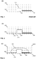
Fig. 1 illustrates one example of amultilayer structure 100 of integrated and embedded electronics. Asubstrate 102 is provided to accommodate a number ofelectronic components 104 and a number ofconductor traces 106 for connecting theelectronic components 104. Additionally, atop layer 108 is provided on top of theelectronic components 104 andsubstrate layer 102 as a support structure using a suitable lamination method involving the use of e.g. adhesives, elevated temperatures and/or pressure. - However, one drawback of the prior art solution is that the
electronic components 104 may easily crack or break when thetop layer 108 is provided on top of theelectronic components 104. InFigure 1 a prospective crack in the component is illustrated with adashed line 110. For example the regulation of the pressure/temperature to maintain it at a decent level during the lamination is challenging. If the pressure/temperature is too high thecomponents 104 may crack or break, and on the other hand if the pressure/temperature is too low the composition of thetop layer 108 turns out incorrect and/or the top layer is not attached properly, for instance. The cracking or breaking of theelectronic components 104 during the manufacturing process cause increase in manufacturing costs for multilayer structural electronic devices. Therefore there exists a need for improving the manufacturing procedure of the multilayer structures for the electronic devices.US20090154182 exhibits an electrical device including a circuit board with electrical components, which are encapsulated with a polymer material.US20130062652 discloses lenses on a substrate covered with a thermoformed layer and overmolded with a thermoplastic material - An objective of the invention is to present a multilayer structure and method for an electronic device at least alleviating one or more of the defects of the prior art described above.
- The objectives of the invention are reached by a multilayer structure and a method as defined by the respective independent claims. Various embodiments of the multilayer structure and the method for an electronic device provide a solution to protect and optionally secure the electronics when a further top layer is provided on top of the electronics or from environmental conditions such as moisture, heat, cold, dirt, shocks, etc.
- According to a first aspect a multilayer structure for an electronic device comprises a flexible substrate film for accommodating electronics; at least one electronic component provided on said substrate film; and a number of conductive traces provided on said substrate film for electrically powering and/or connecting electronics including said at least one electronic component, wherein at least one cover is attached to said substrate film on top of said at least one electronic component, being overmolded with thermoplastic material.
- Said cover is or comprises plastic, thermoformed so as to substantially define a dome or other applicable cap shape for accommodating underlying electronics.
- The at least one cover may comprise a single cover placed on top of a plurality of electronic components. Alternatively or in addition, the multilayer structure may comprise at least two covers placed at least partially on top of at least two electronic components, respectively. A plurality of at least functionally separate covers may be physically provided as a one continuous, optionally monolithic, object or as a plurality of discrete physical objects.
- The substrate film (surface) may be encompassed partially or completely by at least one, preferably plastic, cover. The at least one cover may define a number of optionally rounded, preferably dome-shaped, protective caps for electronics. Additionally, the at least one cover may comprise optically transparent or translucent material having regard to predefined electromagnetic wavelengths including wavelengths of e.g. visible spectrum. The at least one cover may further comprise or define a number of through-holes configured, for instance, to enable the light emitted and/or captured by the at least one electronic component to propagate therewithin and outcouple therefrom.
- The substrate film may comprise optically transparent or translucent material as to predefined electromagnetic wavelengths including wavelengths of e.g. visible spectrum.
- Also the thermoplastic material may comprise optically transparent or translucent material having regard to predefined wavelengths including e.g. wavelengths of visible spectrum. The thermoplastic material may optionally comprise a plurality of layers, wherein different layers may exhibit different properties such as elasticity, optical transparency/transmittance, glass transition temperature, and/or melting point.
- The at least one electronic component may include at least one optoelectronic, light-emitting, light-detecting, and/or light-sensing component, preferably a LED (light-emitting diode) or photodiode. Alternatively or additionally it may include e.g. a communications, memory and/or processing element, optionally in a form of an integrated circuit. For example, a microcontroller or a communication chip may be included.
- According to a second aspect, an electronic device is provided. The electronic device is optionally a light-emitting device, light-detecting device, light-sensing device, smart garment or other wearable electronics, smart compression garment, wristop device, armband device, cellular device, tablet, phablet, controller device, computer mouse, joystick, other computer accessory, a display device, vehicle or in-vehicle (e.g. dashboard) electronics, or e.g. a laptop computer, comprising an embodiment of the multilayer structure as described above.
- According to a third aspect, a method for manufacturing a multilayer structure for an electronic device is provided. The method comprises steps of obtaining a flexible substrate film for accommodating electronics; providing, preferably printing, a number of conductor traces on said substrate film for electrically powering and/or connecting electronic components and/or a number of predefined areas on the substrate; providing at least one electronic component on said substrate film, preferably by means of printed electronics and/or surface mounting; placing at least one cover at least partially on top of said at least one electronic component; attaching said at least one cover to said substrate film; and molding thermoplastic material on said at least one cover and substrate film accommodating the electronic components.
- The method comprises initially thermoforming the cover.
- The selected printing method may be one of so-called printed electronics printing methods including e.g. screen printing and ink jetting. Preferably, additive manufacturing such as additive printing technology is thus applied in connection with embodiments of the present invention.
- The attaching may comprise securing the at least one cover with adhesive, soldering, and/or mechanical fixing such as hook and loop fasteners. The molding may comprise injection molding. The method may further comprise providing a number of through-holes to the cover to enable the light emitted, detected and/or sensed by the at least one component to propagate therewithin and outcouple therefrom.
- The expression "a number of" may herein refer to any positive integer starting from one (1).
- The expression "a plurality of" may refer to any positive integer starting from two (2), respectively.
- The exemplary embodiments of the invention presented in this patent application are not to be interpreted to pose limitations to the applicability of the appended claims. The verb "to comprise" is used in this patent application as an open limitation that does not exclude the existence of also un-recited features. The features recited in depending claims are mutually freely combinable unless otherwise explicitly stated.
- The novel features which are considered as characteristic of the invention are set forth in particular in the appended claims. The invention itself, however, both as to its construction and its method of operation, together with additional objectives and advantages thereof, will be best understood from the following description of specific embodiments when read in connection with the accompanying drawings.
- The embodiments of the invention are illustrated by way of example, and not by way of limitation, in the figures of the accompanying drawings.
-
Figure 1 illustrates one example of a prior art multilayer structure. -
Figure 2 illustrates a side view of an embodiment of a multilayer structure according to the present invention. -
Figure 3 illustrates a side view of a second embodiment of a multilayer structure according to the present invention. -
Figure 4A illustrates a side view of a third embodiment of a multilayer structure according to the present invention. -
Figure 4B illustrates a side view of a fourth embodiment of a multilayer structure according to the present invention. -
Figure 4C illustrates a side view of a fifth embodiment of a multilayer structure according to the present invention. -
Figure 5 illustrates a flow diagram disclosing an embodiment of a method according to the present invention. -
Figure 2 illustrates a side view of an embodiment of a planartype multilayer structure 200 according to the present invention comprising asubstrate film 202, at least oneelectronic component 204, at least one, preferably thermoformed,cover 210, and at least onethermoplastic material layer 208. Thesubstrate 202, preferably a flexible plastic film, foil, or sheet, is shown as cut and/or otherwise configured into a substantially rectangular or other desired shape. Thesubstrate 202 may be generally shaped according to the requirements set by each use scenario. It may also exhibit e.g. a circular or square general shape. - The
substrate film 202 may substantially consist of or at least comprise one material selected from the group consisting of: polymer, thermoplastic material, PMMA (Polymethyl methacrylate), Poly Carbonate (PC), polyimide, a copolymer of Methyl Methacrylate and Styrene (MS resin), glass and Polyethylene Terephthalate (PET). - In some embodiments, the
substrate film 202 may be coated or covered by further material layers e.g. on the side facing the environment (i.e. not the electronics). E.g. a textile layer or biological or bio-based materials (e.g. leather, wood, paper, cardboard) in addition to or instead of more conventional additional layers may be provided. Also e.g. rubber or generally rubberous material may be used. - Additionally, the
substrate film 202 may at least partially be optically substantially opaque or at least translucent, if not transparent, having regard to predefined wavelengths e.g. in visible spectrum. Thesubstrate film 202 may have been initially provided with visually distinguishable, decorative/aesthetic and/or informative, features such as graphical pattern thereon. The features may have been provided on the same side of thesubstrate film 202 with theelectronics 204 so that they have been also sealed by the overmoldedplastic material layer 208. Accordingly, IML (in-mold labeling) or IMD (in-mold decoration) technique may be thus applied in the manufacturing phase. Optionally, a number of optical features could be provided by surface relief forms such as grooves or protrusions of thesubstrate film 202. Such features could be obtained by embossing, carving, stamping, molding, etc. - The
substrate film 202 may contain recesses, notches, cuts or openings for providing optical path and/or e.g. access to the elements provided on thesubstrate film 202, on either side thereof. For example, for enabling a battery change (of embedded battery) or generally component change, or for accessing a UI (user interface) feature (e.g. touch-sensitive area, button or switch) thesubstrate film 202 could be provided with a related access route. - The
multilayer structure 200 presented inFigure 2 comprises at least oneelectronic component 204 that is provided on thesubstrate film 202. The multilayer structures may compriseelectronics 204 including one or more electronic components such as passive components and/or active components, which may comprise optoelectronic component(s). The optoelectronic component(s) may include a number of LEDs (light-emitting diode), or other light-emitting components, for example. Alternatively or additionally, the component(s) may include a light-receiving or light-sensitive component such as a photodiode, photoresistor, other photodetector, or e.g. a photovoltaic cell. - The
electronics 204 may include at least one element selected from the group consisting of: optoelectronic component, microcontroller, microprosessor, signal processor, DSP (digital signal processor), sensor, programmable logic chip, memory, transistor, resistor, capacitor, inductor, memory array, memory chip, data interface, transceiver, wireless transceiver, transmitter, receiver, wireless transmitter, and wireless receiver. Different sensing and/or other functionalities may be implemented by the embedded ICs, dedicated components, or shared ICs/electronics (multi-purpose electronics). - The
electronics 204 may include printed electronics obtained by printed electronics technology such as screen printing or ink jetting. Additionally or alternatively, theelectronics 204 may include e.g. surface-mounted elements. For example, adhesive may be utilized for mechanically securing the electronics on the substrate. - Electrical connections such as a number of
traces 206 between theelectronic components 204 or between the electronic component(s) 204 and e.g. external electronics disposed outside the multilayer structure may be provided by conductors and contact areas, which may be printed, for instance, on thesubstrate 202 by means of printed electronics and e.g. conductive ink. The conductive traces 206 may be used for power supply and signalling of control and/or other data. Conductive materials such as conductive adhesive and/or solder may be applied for establishing electrical and also mechanical connections. - The
cover 210 defining e.g. a protective cap may be placed at least partially on top of theelectronic component 204. Thecover 210 is configured to be attached to thesubstrate film 202 with e.g. adhesive, solder, and/or mechanical fixing such as screws, nails, bolts, or hook and loop fasteners (colloquially known as Velcro) applicable for securing thethermoformed cover 210 on thesubstrate film 202. Thecover 210 protects and optionally secures theelectronic components 204 whenthermoplastic material 208 is further molded on thesubstrate film 202 already accommodating theelectronic components 204. Additionally, thecover 210, which may indeed define a protective cap for the underlying electronics, may be configured to protect theelectronics 204 from e.g. environmental conditions such as moisture, heat, cold, dirt, shocks, etc. Thermoforming from plastic sheet or film is a fast and low-cost procedure to obtain a cover with desired shapes to protect and secure theelectronic components 204. Additionally, the placing and attaching of thecover 210 may be provided so that theelectronic components 204 are not damaged. - The
cover 210 may substantially consist of or at least comprise at least one material selected from the group consisting of: polymer, thermoplastic material, PMMA (Polymethyl methacrylate), Poly Carbonate (PC), polyimide, a copolymer of Methyl Methacrylate and Styrene (MS resin), glass and Polyethylene Terephthalate (PET). Thecover 210 may also consist of or comprise rubber or rubbery material, e.g. natural rubber such as latex or synthetic rubber such as styrene butadiene (SBR), polybutadiene (BR), polyether urethane (EU), or fluoro silicone (FMQ), etc. The elasticity of the rubbery material may be preferable at some situations. Additionally, thecover 210 may also consist of or at least comprise conductive metallic material such as aluminium, copper or other similar materials to provide e.g. a Faraday cage around theelectronic components 204 to protect thecomponents 204 from electric charges. - The material of
cover 210 may in some embodiments be opaque. Alternatively, it may at least partially be optically transparent or translucent so that the visible light and/or electromagnetic radiation at some other predefined wavelength(s) are enabled to pass through it with negligible loss. The transmittance may be at least about 80%, 85%, 90%, or 95% at those wavelength(s). Alternatively or in addition, thethermoformed cover 210 may comprise a number of through-holes, cuts, and/or openings configured to enable e.g. the light emitted, detected and/or sensed by at least oneelectronic component 204 to propagate therewithin and outcouple therefrom. Generally, the holes or cuts may enable more efficient interaction of the embedded electronics with the environment outside thecover 210. - The shape and generally dimensions of the
cover 210 may be decided application-specifically. The shape may be angular, rounded e.g. dome-shaped etc. The rounded-shapedcover 210 may exhibit better pressure distribution and/or durability. The shape and/or dimensions of thecover 210 may also be defined according to the shape and/or dimensions of the relatingelectronic components 204. Thecover 210 may coat partially or completely the surface of thesubstrate film 202 that accommodates theelectronic components 204. InFigure 2 thecover 210 extends at the edges of thesubstrate film 202 to overlay the (top surface of the)substrate film 202 completely. Alternatively, thecover 210 could overlap thesubstrate film 202 partially as illustrated inFigure 2 , where thecover 210 might alternatively end e.g. at the location of a dashedline 212. - Instead of or in addition to opaque material, the molded
thermoplastic material 208 may comprise optically substantially transparent or translucent material so as to enable the visible light and/or electromagnetic radiation at some other predefined wavelength(s) to pass through it with negligible loss. The transmittance may be at least about 80%, 85%, 90%, or 95% at those wavelength(s). The radiation/light may be emitted, detected and/or sensed by theelectronics 204 provided on thesubstrate film 202. The shape and generally dimensions of the moldedlayer 208 may be decided application-specifically. InFigure 2 , the moldedlayer 208 exhibits a rectangular profile but e.g. a rounded profile is possible as well. - The thermoplastic material may comprise multiple layers, which is illustrated with a side view of an embodiment in
Figure 3 . The materials ofthermoplastic layers - In some optional embodiments as indicated by numeral 202B and the dashed potentially missing/removed
portion 304B of moldedsecond material 304 thereon, one or more edges or edge areas of thesubstrate 202 may indeed be left unmolded or the molded material may be removed therefrom afterwards so that e.g. electrical coupling to external elements and/or mounting is facilitated. Such edge portions may accommodate part of theconductors 206 for the purpose. Alternatively or additionally, the electrical coupling elements such as conductors could be funnelled from the inside of themultilayer structure 300 to the border/edge therefor in favour of external connectivity even if thesubstrate edge 202B was not kept free from the molded material. -
Figure 4A presents a side view of one embodiment of e.g. planartype multilayer structure 400a according to the present invention comprisingsubstrate film 202, a number ofelectronic components 204, one preferablythermoformed cover 210, and at least onethermoplastic material layer 208 molded thereon. The considerations set forth regardingFigure 2 or Figure 3 generally apply also here and vice versa what comes to properties and configuration of different materials, dimensions, electronics, etc. Thecover 210 may be placed at least partially on top of the multipleelectronic components 204 for protecting and securing the electronic components 2104 when thethermoplastic material 208 is molded on thesubstrate film 202 accommodating theelectronic components 204. - Another embodiment of a planar
type multilayer structure 400b according to the present invention comprisingsubstrate film 202, a number ofelectronic components 204, a plurality of at least functionally separable (e.g. in the light of target electronics such as components such as passive components or chips to be protected) if not physically separate, preferably thermoformed, covers 210, and at least onethermoplastic material layer 208 is illustrated inFigure 4B . The considerations set forth regardingFigure 2 or 3 generally apply also here and vice versa what comes to properties and configuration of different materials, dimensions, electronics, etc. Eachcover 210 of said number may be placed at least partially on top of exactly one or at least oneelectronic component 204 for protecting and securing the underlying electronic component(s) 204 when thethermoplastic material 208 is molded on thesubstrate film 202 accommodating thecomponents 204. - Some optional embodiments of multilayer structures according to the present invention may comprise combinations of the features of the embodiments presented in
Figures 4A and 4B. Figure 4C thus illustrates a side view of one further embodiment, which discloses amultilayer structure 400c comprising a number ofelectronic components 204 and a number of preferably thermoformed covers 210, so that at least onecover 210 may be placed at least partially on top of exactly oneelectronic component 204 and at least oneother cover 210 may be placed at least partially on top of a plurality ofelectronic components 204. - As alluded to above, the
cover 210 layer may define or incorporate a substantially continuous piece or object of material for a plurality of thermoformed covers and/or discrete item for each thermoformed cover. In other words, functionally a plurality of thermoformed covers 210 may be provided as a one physically continuous object defining multiple suitable cover shapes such as domes or recesses depending on the viewpoint for the underlying electronics as illustrated inFigure 4B , or each of the thermoformed covers 210 may be provided as a discrete object as illustrated inFigure 4C (on the right), or a combination of these approaches may be used to provide the thermoformed covers. A single cover or object of multiple covers may comprise one or more different materials. The cover materials may mutually differ even within a multilayer structure. And, the cover(s) 210 may at least collectively extend substantially completely over the surface of theconcerned substrate film 202 that accommodates theelectronics 204 as presented inFigures 4A and 4B , or the overlap may only be partial as presented inFigure 4C . - The dimensions and the thickness of the
thermoformed cover 210 may vary from an embodiment to another. For example the dimensions may be defined by the dimensions of the electronic component(s) 204. The thickness of the established multilayer structure may be few hundreds of microns or one or few millimetres, for instance. Accordingly, the thickness of the moldedthermoplastic layer thermoplastic layer electronic components 204 may be generally similar or smaller so that the structure can still host and embed them to a sufficient extent. The dimensions and thickness of thesubstrate film 202 may also vary from an embodiment to another. The thickness may be about 100 microns or few hundred microns, or a millimetre, for instance. The dimensions of thecover 210 may generally be similar, for instance. Wall thicknesses of thecover 210 may be considerably less than the actual height of thecover 210 as the cover may define dome or other hollow space for accommodating protrusions ofelectronics 204 on thesubstrate 202 . The dimensions of the features of the embodiments illustrated in Figures are not in any particularly preferred scale with each other but have been mainly selected for clarity reasons instead. - Multilayer structures presented herein may find use in various electronic devices. For example, a portable electronic apparatus such as a wristop device could be provided with an embodiment of the structure, the structure optionally forming at least part of the associated wristband. Alternatively or additionally, the multilayer structures may be used in a light-emitting device, light-detecting device, light-sensing device, smart garment/wearable electronics, armband device, cellular device, tablet, phablet, controller device, computer mouse, joystick, other computer accessory, a display device, or a laptop computer. The suggested solution may further find use in vehicle electronics.
-
Figure 5 is a flow diagram disclosing an embodiment of a method according to the present invention. - At the beginning of the method for manufacturing the multilayer structure, a start-up
phase 502 may be executed. During start-up 502, the necessary tasks such as material, component and tools selection, acquisition, calibration and other configuration may take place. Specific care must be taken that the individual elements and material selections work together and survive the selected manufacturing and installation process, which is naturally preferably checked up-front on the basis of the manufacturing process specifications and component data sheets, or by investigating and testing the produced prototypes, for example. The used equipment such as molding/IMD (in-mold decoration), lamination, bonding, thermoforming, and/or printing equipment, among others, may be thus ramped up to operational status at this stage. - At 504, at least one, preferably flexible, substrate film for accommodating electronics is obtained. A ready-made element of substrate material, e.g. roll of plastic film, may be acquired. In some embodiments the substrate film itself may be first produced in-house by molding or other methods from the desired starting material(s). Optionally, the substrate film is processed. It may be, for example, provided with openings, notches, recesses, cuts, reliefs, etc.
- At 506, a number of conductive elements, such as conductor traces and contact areas (e.g. pads) for electrically coupling to the electronic components are provided on the substrate, preferably by one or more techniques of printed electronics. For example, screen, inkjet, flexographic, gravure or offset lithographic printing may be utilized. The traces may provide necessary electrical interconnections between the components and electronics in general.
- At 508, electronics are provided on the substrate. Ready-made components such as various SMDs (surface-mount device) may be attached to the contact areas by solder and adhesives. Alternatively or additionally, printed electronics technology may be applied to actually manufacture at least part of the components, such as OLEDs (Organic LED), directly onto the film.
- At 510, at least one cover for protecting and securing the electronic components is obtained. It is typically thermoformed. The thermoforming of the cover may be done by using a mold corresponding to the related electronic components, so that cover material is shaped in the presence of suction/heat according to the shape of the mold. The cover is configured to be attached 512 to the substrate film on top of the electronic component(s) with e.g. adhesive, soldering, and/or mechanical fixing such as hook and loop fasteners (colloquially known as Velcro). Alternatively or additionally, the cover(s) may be produced directly on top of the related electronic component provided on substrate film. The covers may be provided well in advance and a number of covers provided in advance may be stored in the meantime. The covers may also be purchased as ready-made or almost ready-made.
- In some embodiments, a number of through-holes may be provided 520 to the cover to enable e.g. the light emitted, detected and/or sensed by the at least one component to propagate therewithin and outcouple therefrom. The through-holes may be for example drilled or stamped through the cover after e.g. thermoforming and before attaching the cover to the substrate film on top of the electronic components. Alternatively, the through-hole may be provided to the cover before e.g. thermoforming. In case the cover is manufactured by molding, hole(s) may be produced by proper mold design. The though-holes may enable the thermoplastic material to be molded through the through-holes also inside the cover between the cover and the electronics. Alternatively, the through-holes may be dimensioned so that the molded thermoplastic material will not enter the through-hole during the molding procedure or enters the hole and following space e.g. in a limited, more controllable fashion.
- At 514, the thermoplastic material is molded upon at least one side of the substrate film and at least partially covered electronics thereon, such as a number of electronic components, related traces and contact areas. The applicable molding methods include injection molding, for instance. In some embodiments a plurality of thermoplastic material layers may be utilized. The plurality of thermoplastic materials may be molded using a multi-shot molding method. A molding machine with multiple molding units may be utilized. Alternatively, multiple machines or a single re-configurable machine could be used for sequentially providing the materials.
-
Item 516, refers to possible post-processing tasks. Further layers may be added into the multilayer structure. The layers may be of indicative or aesthetic value, for instance, and contain e.g. textile or rubber materials instead of or in addition to further plastics. The structure may be installed at a host device or host element such as a piece of footwear (e.g. shoes or (in)sole), helmet, shirt, trousers, compression garment, other garment, etc. Further elements such as electronics may be installed at the outer surface(s) of the structure, such as the exterior surface of the substrate. - At 518, method execution is ended.
- Features reviewed in the preceding description may be used in combinations other than the combinations explicitly indicated. Although certain functions have been described with reference to certain features, those functions may be performable by other features whether described or not. Although some features have been described with reference to certain embodiments only, those features may also be present in other embodiments whether described or not.
Claims (18)
- A multilayer structure (200, 300, 400a, 400b, 400c) for an electronic device, comprising
a flexible substrate film (202) for accommodating electronics (204),
at least one electronic component (204) provided on said substrate film (202), a number of conductive traces (206) provided on said substrate film (202) for electrically powering and/or connecting electronics including said at least one electronic component (204), characterised in that at least one, thermoformed, cover (210) is attached to said substrate film (202) on top of said at least one electronic component (204), being overmolded with thermoplastic material (208). - The structure of claim 1, wherein said at least one cover comprises a cover (400a, 210) placed at on top of a plurality of electronic components (204).
- The structure of any preceding claim, comprising at least two covers (400c, 210) placed at least partially on top of at least two electronic components (204) respectively.
- The structure of any preceding claim, wherein a continuous, optionally monolithic, object (400b, 210) defines multiple cover shapes, each cover shape being configured to accommodate one or more electronic components
- The structure of any preceding claim, wherein said at least one cover (210) extends over the surface of the substrate film (202) accommodating said at least one electronic component partially or completely.
- The structure of any preceding claim, wherein said at least one cover (210) defines a number of optionally rounded, preferably dome-shaped, protective caps for electronics (204).
- The structure of any preceding claim, wherein said at least one cover (210) comprises optically transparent or translucent material having regard to predefined electromagnetic wavelengths preferably including wavelengths of visible spectrum.
- The structure of any preceding claim, wherein said at least one cover (210) comprises a number of through-holes optionally configured to enable the light emitted and/or detected by the at least one electronic component (201) to propagate therewithin and outcouple therefrom.
- The structure of any preceding claim, wherein said substrate film (202) comprises optically transparent or translucent material as to predetermined electromagnetic wavelengths preferably including wavelengths of visible spectrum.
- The structure of any preceding claim, wherein said thermoplastic material (208) comprises optically transparent or translucent material having regard to predefined wavelengths preferably including wavelengths of visible spectrum.
- The structure of any preceding claim, wherein said thermoplastic material comprises a plurality of layers (302, 304), wherein the thermoplastic material layers (302, 304) exhibit different elasticities, optical transparencies/transmittances, glass transition temperatures, and/or melting points.
- The structure of any preceding claim, wherein said at least one electronic component (204) includes at least one optoelectronic, light-emitting, light-detecting, and/or light-sensing component, preferably a LED (light-emitting diode) or photodiode.
- An electronic device, optionally a light-emitting device, light-detecting device, light-sensing device, smart garment, smart compression garment, wristop device, armband device, cellular device, tablet, phablet, controller device, computer mouse, joystick, other computer accessory, a display device, or a laptop computer, comprising the structure of any preceding claim.
- A method for manufacturing a multilayer structure for an electronic device, comprising
obtaining a flexible substrate film for accommodating electronics (504),
providing, preferably printing, a number of conductor traces on said substrate film for electrically powering and/or connecting electronic components and/or a number of predefined areas on the substrate (506),
providing at least one electronic component on said substrate film (508), preferably by means of printed electronics and/or surface mounting,
placing at least one thermoformed cover at least partially on top of said at least one electronic component (510),
attaching said at least one cover to said substrate film (512), and
molding a thermoplastic material on said at least one thermoformed cover and substrate film accommodating the electronic components (514). - The method of claim 14, further comprising thermoforming the cover.
- The method of any of claims 14-15, wherein said attaching comprises securing the at least one cover with adhesive, soldering, and/or mechanical fixing such as hook and loop fasteners.
- The method of any of claims 14-16, wherein said molding comprises injection molding.
- The method of any of claims 14-17, comprising providing a number of through-holes to the cover to enable the light emitted, detected and/or sensed by the at least one component to propagate therewithin and outcouple therefrom (520).
Applications Claiming Priority (2)
| Application Number | Priority Date | Filing Date | Title |
|---|---|---|---|
| US201562163410P | 2015-05-19 | 2015-05-19 | |
| PCT/FI2016/050337 WO2016185096A1 (en) | 2015-05-19 | 2016-05-19 | Thermoformed plastic cover for electronics and related method of manufacture |
Publications (3)
| Publication Number | Publication Date |
|---|---|
| EP3297827A1 EP3297827A1 (en) | 2018-03-28 |
| EP3297827A4 EP3297827A4 (en) | 2019-01-09 |
| EP3297827B1 true EP3297827B1 (en) | 2020-03-11 |
Family
ID=57319490
Family Applications (1)
| Application Number | Title | Priority Date | Filing Date |
|---|---|---|---|
| EP16795951.9A Active EP3297827B1 (en) | 2015-05-19 | 2016-05-19 | Thermoformed plastic cover for electronics and related method of manufacture |
Country Status (8)
| Country | Link |
|---|---|
| US (2) | US10064282B2 (en) |
| EP (1) | EP3297827B1 (en) |
| JP (1) | JP6784701B2 (en) |
| KR (1) | KR102366620B1 (en) |
| CN (1) | CN107709007B (en) |
| MX (1) | MX2017014803A (en) |
| TW (1) | TW201703208A (en) |
| WO (1) | WO2016185096A1 (en) |
Families Citing this family (33)
| Publication number | Priority date | Publication date | Assignee | Title |
|---|---|---|---|---|
| CN107709007B (en) * | 2015-05-19 | 2021-01-05 | 塔科图特科有限责任公司 | Thermoformed plastic cover for electronic device and associated manufacturing method |
| WO2018138892A1 (en) * | 2017-01-27 | 2018-08-02 | 三菱電機株式会社 | Display unit, display device and method for manufacturing display unit |
| US11665830B2 (en) * | 2017-06-28 | 2023-05-30 | Honda Motor Co., Ltd. | Method of making smart functional leather |
| EP3421278B1 (en) * | 2017-06-29 | 2022-10-19 | PLASMAN Europe AB | Illuminated decorative strip |
| US10768358B2 (en) | 2017-08-17 | 2020-09-08 | Dura Operating, Llc | Printed film with mounted light emitting diodes encapsulated in light guide |
| US11685102B2 (en) | 2017-11-08 | 2023-06-27 | Hytech Worldwide, Inc. | Three dimensional thermoforming and lamination |
| US10807300B2 (en) * | 2017-11-08 | 2020-10-20 | Hytech Worldwide, Inc. | Three dimensional thermoforming of plastics with electronic components |
| US10715140B2 (en) | 2017-11-30 | 2020-07-14 | Dura Operating, Llc | Laminated light guide and electrical component carrier |
| US10055530B1 (en) * | 2017-12-13 | 2018-08-21 | Tactotek Oy | Arrangement and method for facilitating electronics design in connection with 3D structures |
| US10219368B1 (en) | 2017-12-22 | 2019-02-26 | Dura Operating, Llc | Laminated light guide and carrier having a circuit board with light emitting diodes and through bores with a light guide disposed therein with an opaque film overlapping the through bore |
| US10564341B2 (en) | 2017-12-22 | 2020-02-18 | Dura Operating, Llc | Light guide and printed circuit board film positioner |
| US10656317B2 (en) | 2017-12-22 | 2020-05-19 | Dura Operating, Llc | Laminated printed circuit board with over-molded light guide |
| US11143597B2 (en) | 2018-01-25 | 2021-10-12 | Xerox Corporation | Water ingress indicator for electronic devices |
| US10669054B1 (en) | 2018-03-19 | 2020-06-02 | Amazon Technologies, Inc. | Right-sized thermoformed cavities for packaging items |
| US10939544B2 (en) | 2018-05-10 | 2021-03-02 | Dura Operating, Llc | Multiple resin over-mold for printed circuit board electronics and light guide |
| US10688916B2 (en) | 2018-05-10 | 2020-06-23 | Dura Operating, Llc | Multiple resin over-mold for printed circuit board electronics and light guide |
| US20210249316A1 (en) | 2018-07-16 | 2021-08-12 | Nano Dimension Technologies Ltd. | Methods and system of improving connectivity of integrated components embedded in a host structure |
| CN108738234A (en) * | 2018-07-31 | 2018-11-02 | 北京梦之墨科技有限公司 | A kind of low-melting-point metal circuit board and preparation method thereof |
| GB2577286B (en) | 2018-09-19 | 2022-12-14 | Conductive Transfers Ltd | Transfer including an electrical component |
| WO2020086863A1 (en) * | 2018-10-25 | 2020-04-30 | Jabil Inc. | Printing of multilayer circuits on graphics |
| US11857299B2 (en) * | 2018-12-27 | 2024-01-02 | Polar Electro Oy | Wearable heart activity sensor device |
| EP3673797A1 (en) * | 2018-12-27 | 2020-07-01 | Polar Electro Oy | Wearable heart activity sensor device |
| US11166363B2 (en) | 2019-01-11 | 2021-11-02 | Tactotek Oy | Electrical node, method for manufacturing electrical node and multilayer structure comprising electrical node |
| CN110324973B (en) * | 2019-08-07 | 2022-10-28 | 深圳市恒翊科技有限公司 | Film-coated injection-molded circuit structure and method for manufacturing same |
| EP3787381A1 (en) * | 2019-08-30 | 2021-03-03 | Nederlandse Organisatie voor toegepast- natuurwetenschappelijk Onderzoek TNO | Electronic device with multilayer laminate |
| CN111836462B (en) * | 2020-08-03 | 2022-02-01 | Oppo广东移动通信有限公司 | Wearable device |
| CN114430624B (en) * | 2020-10-29 | 2024-03-15 | 鹏鼎控股(深圳)股份有限公司 | Circuit board manufacturing method and circuit board |
| JP7143046B2 (en) * | 2020-12-07 | 2022-09-28 | Nissha株式会社 | Resin case with electronic parts and its manufacturing method |
| KR102486207B1 (en) * | 2021-02-10 | 2023-01-10 | 주식회사 파이헬스케어 | Substrate for light source and fabricating method thereof |
| US20220302329A1 (en) * | 2021-03-19 | 2022-09-22 | GAF Energy LLC | Photovoltaic module with a laminated potted printed circuit board |
| KR102394587B1 (en) * | 2021-07-19 | 2022-05-06 | 인탑스 주식회사 | Multiple structure of In-mold electronics and method producing the same |
| US11415308B1 (en) | 2021-12-22 | 2022-08-16 | Neil Haney | Curtain lights kit and curtain lights device |
| US20230367427A1 (en) * | 2022-05-12 | 2023-11-16 | Ligitek Electronics Co., Ltd. | Touch Light-Emitting Module and Manufacturing Method Thereof |
Family Cites Families (66)
| Publication number | Priority date | Publication date | Assignee | Title |
|---|---|---|---|---|
| US64282A (en) * | 1867-04-30 | Peters | ||
| JPS62124877U (en) * | 1986-01-30 | 1987-08-08 | ||
| US5718326A (en) * | 1996-07-22 | 1998-02-17 | Delco Electronics Corporation | Backlit button/switchpad assembly |
| US6049463A (en) * | 1997-07-25 | 2000-04-11 | Motorola, Inc. | Microelectronic assembly including an antenna element embedded within a polymeric card, and method for forming same |
| JP3637809B2 (en) * | 1999-05-26 | 2005-04-13 | 松下電工株式会社 | Infrared data communication module |
| US6614103B1 (en) * | 2000-09-01 | 2003-09-02 | General Electric Company | Plastic packaging of LED arrays |
| CN101938829B (en) * | 2000-11-16 | 2012-03-28 | 株式会社Ntt都科摩 | Method of registering position of mobile communication terminal, general calling method for mobile communication terminal and mobile communication method |
| SG104293A1 (en) | 2002-01-09 | 2004-06-21 | Micron Technology Inc | Elimination of rdl using tape base flip chip on flex for die stacking |
| EP1328141B1 (en) * | 2002-01-12 | 2010-11-10 | odelo GmbH | Assembly having a conductor from flexible material and method for manufacturing such an assembly |
| US6682331B1 (en) * | 2002-09-20 | 2004-01-27 | Agilent Technologies, Inc. | Molding apparatus for molding light emitting diode lamps |
| JP4107952B2 (en) | 2002-12-04 | 2008-06-25 | 三洋電機株式会社 | Circuit device manufacturing method |
| US20080102726A2 (en) * | 2003-03-12 | 2008-05-01 | Balu Jeganathan | Lamp and a process for producing a lamp |
| US7128442B2 (en) * | 2003-05-09 | 2006-10-31 | Kian Shin Lee | Illumination unit with a solid-state light generating source, a flexible substrate, and a flexible and optically transparent encapsulant |
| CN1802883A (en) * | 2003-07-03 | 2006-07-12 | 株式会社日立制作所 | Assembly apparatus and its manufacturing method |
| JP4688679B2 (en) * | 2003-09-09 | 2011-05-25 | 三洋電機株式会社 | Semiconductor module |
| JP2005317661A (en) * | 2004-04-27 | 2005-11-10 | Sharp Corp | Semiconductor light emitting device and its manufacturing method |
| JP2006012943A (en) * | 2004-06-23 | 2006-01-12 | Murata Mfg Co Ltd | Electronic device and method of manufacturing the same |
| US20080206549A1 (en) * | 2004-07-14 | 2008-08-28 | Mycoal Products Corporation, | Heat Generating Body |
| US7343675B2 (en) * | 2004-11-12 | 2008-03-18 | Harris Corporation | Method of constructing a structural circuit |
| US7343060B2 (en) * | 2005-03-04 | 2008-03-11 | Fuji Xerox Co., Ltd. | Light transmission and reception module, sub-mount, and method of manufacturing the sub-mount |
| FR2883653B1 (en) * | 2005-03-22 | 2007-05-25 | Gemplus Sa | ELECTRONIC MODULE AND CHIP CARD WITH LUMINOUS INDICATOR |
| US7365371B2 (en) * | 2005-08-04 | 2008-04-29 | Cree, Inc. | Packages for semiconductor light emitting devices utilizing dispensed encapsulants |
| JP4945106B2 (en) * | 2005-09-08 | 2012-06-06 | スタンレー電気株式会社 | Semiconductor light emitting device |
| JP5237540B2 (en) * | 2005-09-20 | 2013-07-17 | パナソニック株式会社 | Light emitting device |
| US8465175B2 (en) * | 2005-11-29 | 2013-06-18 | GE Lighting Solutions, LLC | LED lighting assemblies with thermal overmolding |
| WO2007116452A1 (en) * | 2006-03-30 | 2007-10-18 | Fujitsu Limited | Electronic apparatus, management method, and management program |
| JP2008003254A (en) * | 2006-06-21 | 2008-01-10 | Idemitsu Kosan Co Ltd | Multilayer sheet for beam reflection, and reflector, illuminator and liquid crystal display device using the same |
| WO2008024761A2 (en) * | 2006-08-21 | 2008-02-28 | Innotec Corporation | Electrical device having boardless electrical component mounting arrangement |
| KR20090115803A (en) * | 2007-02-13 | 2009-11-06 | 쓰리엠 이노베이티브 프로퍼티즈 컴파니 | Led devices having lenses and methods of making same |
| US7729570B2 (en) * | 2007-05-18 | 2010-06-01 | Ibiden Co., Ltd. | Photoelectric circuit board and device for optical communication |
| FR2919218B1 (en) * | 2007-07-25 | 2011-12-02 | Faurecia Automotive Ind | INSONORIZATION MOLD COMPONENT AND METHOD FOR MANUFACTURING THE SAME |
| EP2977080B1 (en) * | 2007-07-27 | 2024-02-14 | Cortigent, Inc. | Implantable device for the brain |
| EP2232592B1 (en) * | 2007-12-12 | 2013-07-17 | Innotec Corporation | Method for overmolding a circuit board |
| JP4744573B2 (en) * | 2008-01-23 | 2011-08-10 | サンユレック株式会社 | Manufacturing method of electronic device |
| US7786821B2 (en) * | 2008-06-02 | 2010-08-31 | Bsc Filters Ltd. | Compact end launch transition including a body with an antenna and an electrical connector |
| FI121862B (en) * | 2008-10-24 | 2011-05-13 | Valtion Teknillinen | Arrangement for touch screen and corresponding manufacturing method |
| KR20110085481A (en) * | 2010-01-20 | 2011-07-27 | 삼성전자주식회사 | Stacked semiconductor package |
| US9036359B2 (en) * | 2010-10-15 | 2015-05-19 | Leonovo Innovations Limited (Hong Kong) | Component built-in module, electronic device including same, and method for manufacturing component built-in module |
| JPWO2012049895A1 (en) * | 2010-10-15 | 2014-02-24 | 日本電気株式会社 | Component built-in module, electronic device including the same, and method of manufacturing component built-in module |
| US9395057B2 (en) | 2011-02-07 | 2016-07-19 | Cree, Inc. | Lighting device with flexibly coupled heatsinks |
| US20120315382A1 (en) | 2011-06-10 | 2012-12-13 | Aliphcom | Component protective overmolding using protective external coatings |
| DE102012204630A1 (en) * | 2012-03-22 | 2013-09-26 | Robert Bosch Gmbh | Control device for controlling thermoplastic molding, during manufacturing of e.g. chip, has substrate and electronic component enclosed by mold where device is surrounded by cover over sealing region that is overlapped in exposed region |
| JP6192897B2 (en) * | 2012-04-11 | 2017-09-06 | サターン ライセンシング エルエルシーSaturn Licensing LLC | LIGHT EMITTING DEVICE, DISPLAY DEVICE, AND LIGHTING DEVICE |
| KR102079188B1 (en) * | 2012-05-09 | 2020-02-19 | 가부시키가이샤 한도오따이 에네루기 켄큐쇼 | Light-emitting device and electronic device |
| US10285270B2 (en) * | 2012-09-07 | 2019-05-07 | Joseph Fjelstad | Solder alloy free electronic (safe) rigid-flexible/stretchable circuit assemblies having integral, conductive and heat spreading sections and methods for their manufacture |
| WO2014063060A1 (en) * | 2012-10-19 | 2014-04-24 | Prism Microwave, Inc. | Radio frequency filter assembly |
| EP2743786B1 (en) * | 2012-12-17 | 2018-10-31 | The Swatch Group Research and Development Ltd. | Portable electronic device and method for manufacturing such a device |
| JP5958558B2 (en) * | 2012-12-18 | 2016-08-02 | 株式会社村田製作所 | Resin multilayer board |
| US9254166B2 (en) * | 2013-01-17 | 2016-02-09 | Arthrocare Corporation | Systems and methods for turbinate reduction |
| DE102013102003A1 (en) * | 2013-02-28 | 2014-08-28 | Bundesdruckerei Gmbh | Chip card with integrated active components |
| CN105593921A (en) * | 2013-03-13 | 2016-05-18 | 廷克有限公司 | Automatic sensing methods and devices for inventory control |
| US10108086B2 (en) * | 2013-03-15 | 2018-10-23 | Nanonex Corporation | System and methods of mold/substrate separation for imprint lithography |
| US9657903B2 (en) * | 2013-08-20 | 2017-05-23 | Nthdegree Technologies Worldwide Inc. | Geometrical light extraction structures for printed LEDs |
| JP6414427B2 (en) * | 2013-10-03 | 2018-10-31 | 日亜化学工業株式会社 | Light emitting device mounting structure |
| JP6331688B2 (en) * | 2014-05-23 | 2018-05-30 | 株式会社リコー | Liquid discharge head, method for manufacturing the same, liquid discharge apparatus, and image forming apparatus |
| US10421218B2 (en) * | 2014-06-03 | 2019-09-24 | Scivax Corporation | Roller-type depressing device, imprinting device, and roller-type depressing method |
| KR20160006891A (en) * | 2014-07-09 | 2016-01-20 | 삼성전자주식회사 | Light source module and lighting device having the same |
| US9304335B2 (en) * | 2014-07-16 | 2016-04-05 | Globalfoundries Inc. | Integrated LDMOS devices for silicon photonics |
| US20160070339A1 (en) * | 2014-09-08 | 2016-03-10 | Aliphcom | Divice-based activity classification using predictive feature analysis |
| US20160066859A1 (en) * | 2014-09-08 | 2016-03-10 | Aliphcom | Device-based activity classification using predictive feature analysis |
| US20160072554A1 (en) * | 2014-09-08 | 2016-03-10 | Aliphcom | Near-field antennas and methods of implementing the same for wearable pods and devices that include metalized interfaces |
| US20160072177A1 (en) * | 2014-09-08 | 2016-03-10 | Aliphcom | Antennas and methods of implementing the same for wearable pods and devices that include metalized interfaces |
| US10091887B2 (en) * | 2015-04-02 | 2018-10-02 | Tactotek Oy | Multi-material structure with embedded electronics |
| US10082913B2 (en) * | 2015-05-10 | 2018-09-25 | Microsoft Technology Licensing, Llc | Embroidered sensor assembly |
| CN107709007B (en) * | 2015-05-19 | 2021-01-05 | 塔科图特科有限责任公司 | Thermoformed plastic cover for electronic device and associated manufacturing method |
| JP5988004B1 (en) * | 2016-04-12 | 2016-09-07 | Tdk株式会社 | Electronic circuit package |
-
2016
- 2016-05-19 CN CN201680037545.7A patent/CN107709007B/en active Active
- 2016-05-19 KR KR1020177035848A patent/KR102366620B1/en active IP Right Grant
- 2016-05-19 WO PCT/FI2016/050337 patent/WO2016185096A1/en active Application Filing
- 2016-05-19 MX MX2017014803A patent/MX2017014803A/en unknown
- 2016-05-19 TW TW105115510A patent/TW201703208A/en unknown
- 2016-05-19 US US15/158,645 patent/US10064282B2/en active Active
- 2016-05-19 JP JP2017560136A patent/JP6784701B2/en active Active
- 2016-05-19 EP EP16795951.9A patent/EP3297827B1/en active Active
-
2018
- 2018-03-27 US US15/937,172 patent/US10383232B2/en active Active
Non-Patent Citations (1)
| Title |
|---|
| None * |
Also Published As
| Publication number | Publication date |
|---|---|
| KR20180010208A (en) | 2018-01-30 |
| EP3297827A4 (en) | 2019-01-09 |
| WO2016185096A1 (en) | 2016-11-24 |
| CN107709007B (en) | 2021-01-05 |
| JP6784701B2 (en) | 2020-11-11 |
| WO2016185096A9 (en) | 2017-12-07 |
| US10064282B2 (en) | 2018-08-28 |
| TW201703208A (en) | 2017-01-16 |
| KR102366620B1 (en) | 2022-02-22 |
| US20180220534A1 (en) | 2018-08-02 |
| CN107709007A (en) | 2018-02-16 |
| US20160345437A1 (en) | 2016-11-24 |
| EP3297827A1 (en) | 2018-03-28 |
| MX2017014803A (en) | 2018-05-11 |
| US10383232B2 (en) | 2019-08-13 |
| JP2018524799A (en) | 2018-08-30 |
Similar Documents
| Publication | Publication Date | Title |
|---|---|---|
| US10383232B2 (en) | Thermoformed plastic cover for electronics and related method of manufacture | |
| US10251278B2 (en) | Multi-material structure with embedded electronics | |
| US10248277B2 (en) | Multilayer structure with embedded multilayer electronics | |
| KR102616605B1 (en) | Multilayer structure for accommodating electronics and related method of manufacture | |
| EP3610707B1 (en) | Multilayer structure and related method of manufacture of multilayer structure | |
| JP2019192919A (en) | Multi-layer structure for electronic apparatus and related manufacturing method | |
| US20170094800A1 (en) | Method and arrangement for providing electrical connection to in-mold electronics | |
| EP3357310A1 (en) | Multilayer structure and related method of manufacture for electronics |
Legal Events
| Date | Code | Title | Description |
|---|---|---|---|
| STAA | Information on the status of an ep patent application or granted ep patent |
Free format text: STATUS: THE INTERNATIONAL PUBLICATION HAS BEEN MADE |
|
| PUAI | Public reference made under article 153(3) epc to a published international application that has entered the european phase |
Free format text: ORIGINAL CODE: 0009012 |
|
| STAA | Information on the status of an ep patent application or granted ep patent |
Free format text: STATUS: REQUEST FOR EXAMINATION WAS MADE |
|
| 17P | Request for examination filed |
Effective date: 20171212 |
|
| AK | Designated contracting states |
Kind code of ref document: A1 Designated state(s): AL AT BE BG CH CY CZ DE DK EE ES FI FR GB GR HR HU IE IS IT LI LT LU LV MC MK MT NL NO PL PT RO RS SE SI SK SM TR |
|
| AX | Request for extension of the european patent |
Extension state: BA ME |
|
| DAV | Request for validation of the european patent (deleted) | ||
| DAX | Request for extension of the european patent (deleted) | ||
| A4 | Supplementary search report drawn up and despatched |
Effective date: 20181212 |
|
| RIC1 | Information provided on ipc code assigned before grant |
Ipc: H01L 23/538 20060101ALI20181206BHEP Ipc: H05K 3/28 20060101ALI20181206BHEP Ipc: F21K 9/00 20160101ALI20181206BHEP Ipc: B32B 27/08 20060101AFI20181206BHEP Ipc: H05K 1/03 20060101ALI20181206BHEP Ipc: H05K 5/00 20060101ALI20181206BHEP |
|
| GRAP | Despatch of communication of intention to grant a patent |
Free format text: ORIGINAL CODE: EPIDOSNIGR1 |
|
| STAA | Information on the status of an ep patent application or granted ep patent |
Free format text: STATUS: GRANT OF PATENT IS INTENDED |
|
| INTG | Intention to grant announced |
Effective date: 20191202 |
|
| GRAS | Grant fee paid |
Free format text: ORIGINAL CODE: EPIDOSNIGR3 |
|
| GRAA | (expected) grant |
Free format text: ORIGINAL CODE: 0009210 |
|
| STAA | Information on the status of an ep patent application or granted ep patent |
Free format text: STATUS: THE PATENT HAS BEEN GRANTED |
|
| AK | Designated contracting states |
Kind code of ref document: B1 Designated state(s): AL AT BE BG CH CY CZ DE DK EE ES FI FR GB GR HR HU IE IS IT LI LT LU LV MC MK MT NL NO PL PT RO RS SE SI SK SM TR |
|
| REG | Reference to a national code |
Ref country code: GB Ref legal event code: FG4D |
|
| REG | Reference to a national code |
Ref country code: CH Ref legal event code: EP |
|
| REG | Reference to a national code |
Ref country code: AT Ref legal event code: REF Ref document number: 1242631 Country of ref document: AT Kind code of ref document: T Effective date: 20200315 |
|
| REG | Reference to a national code |
Ref country code: IE Ref legal event code: FG4D |
|
| REG | Reference to a national code |
Ref country code: DE Ref legal event code: R096 Ref document number: 602016031657 Country of ref document: DE |
|
| PG25 | Lapsed in a contracting state [announced via postgrant information from national office to epo] |
Ref country code: FI Free format text: LAPSE BECAUSE OF FAILURE TO SUBMIT A TRANSLATION OF THE DESCRIPTION OR TO PAY THE FEE WITHIN THE PRESCRIBED TIME-LIMIT Effective date: 20200311 Ref country code: RS Free format text: LAPSE BECAUSE OF FAILURE TO SUBMIT A TRANSLATION OF THE DESCRIPTION OR TO PAY THE FEE WITHIN THE PRESCRIBED TIME-LIMIT Effective date: 20200311 Ref country code: NO Free format text: LAPSE BECAUSE OF FAILURE TO SUBMIT A TRANSLATION OF THE DESCRIPTION OR TO PAY THE FEE WITHIN THE PRESCRIBED TIME-LIMIT Effective date: 20200611 |
|
| REG | Reference to a national code |
Ref country code: NL Ref legal event code: MP Effective date: 20200311 |
|
| PG25 | Lapsed in a contracting state [announced via postgrant information from national office to epo] |
Ref country code: GR Free format text: LAPSE BECAUSE OF FAILURE TO SUBMIT A TRANSLATION OF THE DESCRIPTION OR TO PAY THE FEE WITHIN THE PRESCRIBED TIME-LIMIT Effective date: 20200612 Ref country code: BG Free format text: LAPSE BECAUSE OF FAILURE TO SUBMIT A TRANSLATION OF THE DESCRIPTION OR TO PAY THE FEE WITHIN THE PRESCRIBED TIME-LIMIT Effective date: 20200611 Ref country code: SE Free format text: LAPSE BECAUSE OF FAILURE TO SUBMIT A TRANSLATION OF THE DESCRIPTION OR TO PAY THE FEE WITHIN THE PRESCRIBED TIME-LIMIT Effective date: 20200311 Ref country code: HR Free format text: LAPSE BECAUSE OF FAILURE TO SUBMIT A TRANSLATION OF THE DESCRIPTION OR TO PAY THE FEE WITHIN THE PRESCRIBED TIME-LIMIT Effective date: 20200311 Ref country code: LV Free format text: LAPSE BECAUSE OF FAILURE TO SUBMIT A TRANSLATION OF THE DESCRIPTION OR TO PAY THE FEE WITHIN THE PRESCRIBED TIME-LIMIT Effective date: 20200311 |
|
| REG | Reference to a national code |
Ref country code: LT Ref legal event code: MG4D |
|
| PG25 | Lapsed in a contracting state [announced via postgrant information from national office to epo] |
Ref country code: NL Free format text: LAPSE BECAUSE OF FAILURE TO SUBMIT A TRANSLATION OF THE DESCRIPTION OR TO PAY THE FEE WITHIN THE PRESCRIBED TIME-LIMIT Effective date: 20200311 |
|
| PG25 | Lapsed in a contracting state [announced via postgrant information from national office to epo] |
Ref country code: SM Free format text: LAPSE BECAUSE OF FAILURE TO SUBMIT A TRANSLATION OF THE DESCRIPTION OR TO PAY THE FEE WITHIN THE PRESCRIBED TIME-LIMIT Effective date: 20200311 Ref country code: EE Free format text: LAPSE BECAUSE OF FAILURE TO SUBMIT A TRANSLATION OF THE DESCRIPTION OR TO PAY THE FEE WITHIN THE PRESCRIBED TIME-LIMIT Effective date: 20200311 Ref country code: LT Free format text: LAPSE BECAUSE OF FAILURE TO SUBMIT A TRANSLATION OF THE DESCRIPTION OR TO PAY THE FEE WITHIN THE PRESCRIBED TIME-LIMIT Effective date: 20200311 Ref country code: SK Free format text: LAPSE BECAUSE OF FAILURE TO SUBMIT A TRANSLATION OF THE DESCRIPTION OR TO PAY THE FEE WITHIN THE PRESCRIBED TIME-LIMIT Effective date: 20200311 Ref country code: PT Free format text: LAPSE BECAUSE OF FAILURE TO SUBMIT A TRANSLATION OF THE DESCRIPTION OR TO PAY THE FEE WITHIN THE PRESCRIBED TIME-LIMIT Effective date: 20200805 Ref country code: CZ Free format text: LAPSE BECAUSE OF FAILURE TO SUBMIT A TRANSLATION OF THE DESCRIPTION OR TO PAY THE FEE WITHIN THE PRESCRIBED TIME-LIMIT Effective date: 20200311 Ref country code: IS Free format text: LAPSE BECAUSE OF FAILURE TO SUBMIT A TRANSLATION OF THE DESCRIPTION OR TO PAY THE FEE WITHIN THE PRESCRIBED TIME-LIMIT Effective date: 20200711 Ref country code: RO Free format text: LAPSE BECAUSE OF FAILURE TO SUBMIT A TRANSLATION OF THE DESCRIPTION OR TO PAY THE FEE WITHIN THE PRESCRIBED TIME-LIMIT Effective date: 20200311 |
|
| REG | Reference to a national code |
Ref country code: AT Ref legal event code: MK05 Ref document number: 1242631 Country of ref document: AT Kind code of ref document: T Effective date: 20200311 |
|
| REG | Reference to a national code |
Ref country code: DE Ref legal event code: R097 Ref document number: 602016031657 Country of ref document: DE |
|
| PLBE | No opposition filed within time limit |
Free format text: ORIGINAL CODE: 0009261 |
|
| STAA | Information on the status of an ep patent application or granted ep patent |
Free format text: STATUS: NO OPPOSITION FILED WITHIN TIME LIMIT |
|
| PG25 | Lapsed in a contracting state [announced via postgrant information from national office to epo] |
Ref country code: ES Free format text: LAPSE BECAUSE OF FAILURE TO SUBMIT A TRANSLATION OF THE DESCRIPTION OR TO PAY THE FEE WITHIN THE PRESCRIBED TIME-LIMIT Effective date: 20200311 Ref country code: IT Free format text: LAPSE BECAUSE OF FAILURE TO SUBMIT A TRANSLATION OF THE DESCRIPTION OR TO PAY THE FEE WITHIN THE PRESCRIBED TIME-LIMIT Effective date: 20200311 Ref country code: LI Free format text: LAPSE BECAUSE OF NON-PAYMENT OF DUE FEES Effective date: 20200531 Ref country code: DK Free format text: LAPSE BECAUSE OF FAILURE TO SUBMIT A TRANSLATION OF THE DESCRIPTION OR TO PAY THE FEE WITHIN THE PRESCRIBED TIME-LIMIT Effective date: 20200311 Ref country code: AT Free format text: LAPSE BECAUSE OF FAILURE TO SUBMIT A TRANSLATION OF THE DESCRIPTION OR TO PAY THE FEE WITHIN THE PRESCRIBED TIME-LIMIT Effective date: 20200311 Ref country code: CH Free format text: LAPSE BECAUSE OF NON-PAYMENT OF DUE FEES Effective date: 20200531 Ref country code: MC Free format text: LAPSE BECAUSE OF FAILURE TO SUBMIT A TRANSLATION OF THE DESCRIPTION OR TO PAY THE FEE WITHIN THE PRESCRIBED TIME-LIMIT Effective date: 20200311 |
|
| 26N | No opposition filed |
Effective date: 20201214 |
|
| PG25 | Lapsed in a contracting state [announced via postgrant information from national office to epo] |
Ref country code: SI Free format text: LAPSE BECAUSE OF FAILURE TO SUBMIT A TRANSLATION OF THE DESCRIPTION OR TO PAY THE FEE WITHIN THE PRESCRIBED TIME-LIMIT Effective date: 20200311 Ref country code: PL Free format text: LAPSE BECAUSE OF FAILURE TO SUBMIT A TRANSLATION OF THE DESCRIPTION OR TO PAY THE FEE WITHIN THE PRESCRIBED TIME-LIMIT Effective date: 20200311 |
|
| REG | Reference to a national code |
Ref country code: BE Ref legal event code: MM Effective date: 20200531 |
|
| PG25 | Lapsed in a contracting state [announced via postgrant information from national office to epo] |
Ref country code: LU Free format text: LAPSE BECAUSE OF NON-PAYMENT OF DUE FEES Effective date: 20200519 |
|
| PG25 | Lapsed in a contracting state [announced via postgrant information from national office to epo] |
Ref country code: IE Free format text: LAPSE BECAUSE OF NON-PAYMENT OF DUE FEES Effective date: 20200519 |
|
| PG25 | Lapsed in a contracting state [announced via postgrant information from national office to epo] |
Ref country code: BE Free format text: LAPSE BECAUSE OF NON-PAYMENT OF DUE FEES Effective date: 20200531 |
|
| PG25 | Lapsed in a contracting state [announced via postgrant information from national office to epo] |
Ref country code: TR Free format text: LAPSE BECAUSE OF FAILURE TO SUBMIT A TRANSLATION OF THE DESCRIPTION OR TO PAY THE FEE WITHIN THE PRESCRIBED TIME-LIMIT Effective date: 20200311 Ref country code: MT Free format text: LAPSE BECAUSE OF FAILURE TO SUBMIT A TRANSLATION OF THE DESCRIPTION OR TO PAY THE FEE WITHIN THE PRESCRIBED TIME-LIMIT Effective date: 20200311 Ref country code: CY Free format text: LAPSE BECAUSE OF FAILURE TO SUBMIT A TRANSLATION OF THE DESCRIPTION OR TO PAY THE FEE WITHIN THE PRESCRIBED TIME-LIMIT Effective date: 20200311 |
|
| PG25 | Lapsed in a contracting state [announced via postgrant information from national office to epo] |
Ref country code: MK Free format text: LAPSE BECAUSE OF FAILURE TO SUBMIT A TRANSLATION OF THE DESCRIPTION OR TO PAY THE FEE WITHIN THE PRESCRIBED TIME-LIMIT Effective date: 20200311 Ref country code: AL Free format text: LAPSE BECAUSE OF FAILURE TO SUBMIT A TRANSLATION OF THE DESCRIPTION OR TO PAY THE FEE WITHIN THE PRESCRIBED TIME-LIMIT Effective date: 20200311 |
|
| P01 | Opt-out of the competence of the unified patent court (upc) registered |
Effective date: 20230524 |
|
| PGFP | Annual fee paid to national office [announced via postgrant information from national office to epo] |
Ref country code: FR Payment date: 20230516 Year of fee payment: 8 Ref country code: DE Payment date: 20230524 Year of fee payment: 8 |
|
| PGFP | Annual fee paid to national office [announced via postgrant information from national office to epo] |
Ref country code: GB Payment date: 20230523 Year of fee payment: 8 |