EP3297750B1 - Methods and apparatus for forming apertures in a solid state membrane using dielectric breakdown - Google Patents
Methods and apparatus for forming apertures in a solid state membrane using dielectric breakdown Download PDFInfo
- Publication number
- EP3297750B1 EP3297750B1 EP16727070.1A EP16727070A EP3297750B1 EP 3297750 B1 EP3297750 B1 EP 3297750B1 EP 16727070 A EP16727070 A EP 16727070A EP 3297750 B1 EP3297750 B1 EP 3297750B1
- Authority
- EP
- European Patent Office
- Prior art keywords
- membrane
- layer
- aperture
- fluidic
- sub
- Prior art date
- Legal status (The legal status is an assumption and is not a legal conclusion. Google has not performed a legal analysis and makes no representation as to the accuracy of the status listed.)
- Revoked
Links
Images


Classifications
-
- B—PERFORMING OPERATIONS; TRANSPORTING
- B01—PHYSICAL OR CHEMICAL PROCESSES OR APPARATUS IN GENERAL
- B01D—SEPARATION
- B01D67/00—Processes specially adapted for manufacturing semi-permeable membranes for separation processes or apparatus
- B01D67/0039—Inorganic membrane manufacture
- B01D67/0053—Inorganic membrane manufacture by inducing porosity into non porous precursor membranes
- B01D67/006—Inorganic membrane manufacture by inducing porosity into non porous precursor membranes by elimination of segments of the precursor, e.g. nucleation-track membranes, lithography or laser methods
- B01D67/0062—Inorganic membrane manufacture by inducing porosity into non porous precursor membranes by elimination of segments of the precursor, e.g. nucleation-track membranes, lithography or laser methods by micromachining techniques, e.g. using masking and etching steps, photolithography
-
- B—PERFORMING OPERATIONS; TRANSPORTING
- B01—PHYSICAL OR CHEMICAL PROCESSES OR APPARATUS IN GENERAL
- B01D—SEPARATION
- B01D69/00—Semi-permeable membranes for separation processes or apparatus characterised by their form, structure or properties; Manufacturing processes specially adapted therefor
- B01D69/02—Semi-permeable membranes for separation processes or apparatus characterised by their form, structure or properties; Manufacturing processes specially adapted therefor characterised by their properties
-
- B—PERFORMING OPERATIONS; TRANSPORTING
- B01—PHYSICAL OR CHEMICAL PROCESSES OR APPARATUS IN GENERAL
- B01D—SEPARATION
- B01D69/00—Semi-permeable membranes for separation processes or apparatus characterised by their form, structure or properties; Manufacturing processes specially adapted therefor
- B01D69/12—Composite membranes; Ultra-thin membranes
- B01D69/1214—Chemically bonded layers, e.g. cross-linking
-
- C—CHEMISTRY; METALLURGY
- C12—BIOCHEMISTRY; BEER; SPIRITS; WINE; VINEGAR; MICROBIOLOGY; ENZYMOLOGY; MUTATION OR GENETIC ENGINEERING
- C12Q—MEASURING OR TESTING PROCESSES INVOLVING ENZYMES, NUCLEIC ACIDS OR MICROORGANISMS; COMPOSITIONS OR TEST PAPERS THEREFOR; PROCESSES OF PREPARING SUCH COMPOSITIONS; CONDITION-RESPONSIVE CONTROL IN MICROBIOLOGICAL OR ENZYMOLOGICAL PROCESSES
- C12Q1/00—Measuring or testing processes involving enzymes, nucleic acids or microorganisms; Compositions therefor; Processes of preparing such compositions
- C12Q1/68—Measuring or testing processes involving enzymes, nucleic acids or microorganisms; Compositions therefor; Processes of preparing such compositions involving nucleic acids
- C12Q1/6869—Methods for sequencing
-
- C—CHEMISTRY; METALLURGY
- C25—ELECTROLYTIC OR ELECTROPHORETIC PROCESSES; APPARATUS THEREFOR
- C25F—PROCESSES FOR THE ELECTROLYTIC REMOVAL OF MATERIALS FROM OBJECTS; APPARATUS THEREFOR
- C25F3/00—Electrolytic etching or polishing
- C25F3/02—Etching
-
- C—CHEMISTRY; METALLURGY
- C25—ELECTROLYTIC OR ELECTROPHORETIC PROCESSES; APPARATUS THEREFOR
- C25F—PROCESSES FOR THE ELECTROLYTIC REMOVAL OF MATERIALS FROM OBJECTS; APPARATUS THEREFOR
- C25F3/00—Electrolytic etching or polishing
- C25F3/02—Etching
- C25F3/14—Etching locally
-
- C—CHEMISTRY; METALLURGY
- C25—ELECTROLYTIC OR ELECTROPHORETIC PROCESSES; APPARATUS THEREFOR
- C25F—PROCESSES FOR THE ELECTROLYTIC REMOVAL OF MATERIALS FROM OBJECTS; APPARATUS THEREFOR
- C25F7/00—Constructional parts, or assemblies thereof, of cells for electrolytic removal of material from objects; Servicing or operating
-
- G—PHYSICS
- G01—MEASURING; TESTING
- G01N—INVESTIGATING OR ANALYSING MATERIALS BY DETERMINING THEIR CHEMICAL OR PHYSICAL PROPERTIES
- G01N33/00—Investigating or analysing materials by specific methods not covered by groups G01N1/00 - G01N31/00
- G01N33/48—Biological material, e.g. blood, urine; Haemocytometers
- G01N33/483—Physical analysis of biological material
- G01N33/487—Physical analysis of biological material of liquid biological material
- G01N33/48707—Physical analysis of biological material of liquid biological material by electrical means
- G01N33/48721—Investigating individual macromolecules, e.g. by translocation through nanopores
-
- B—PERFORMING OPERATIONS; TRANSPORTING
- B01—PHYSICAL OR CHEMICAL PROCESSES OR APPARATUS IN GENERAL
- B01D—SEPARATION
- B01D2323/00—Details relating to membrane preparation
- B01D2323/42—Details of membrane preparation apparatus
-
- B—PERFORMING OPERATIONS; TRANSPORTING
- B01—PHYSICAL OR CHEMICAL PROCESSES OR APPARATUS IN GENERAL
- B01D—SEPARATION
- B01D2325/00—Details relating to properties of membranes
- B01D2325/02—Details relating to pores or porosity of the membranes
- B01D2325/021—Pore shapes
-
- B—PERFORMING OPERATIONS; TRANSPORTING
- B01—PHYSICAL OR CHEMICAL PROCESSES OR APPARATUS IN GENERAL
- B01D—SEPARATION
- B01D2325/00—Details relating to properties of membranes
- B01D2325/06—Surface irregularities
-
- B—PERFORMING OPERATIONS; TRANSPORTING
- B82—NANOTECHNOLOGY
- B82Y—SPECIFIC USES OR APPLICATIONS OF NANOSTRUCTURES; MEASUREMENT OR ANALYSIS OF NANOSTRUCTURES; MANUFACTURE OR TREATMENT OF NANOSTRUCTURES
- B82Y40/00—Manufacture or treatment of nanostructures
Definitions
- the invention relates to a method and apparatus for forming single or multiple apertures in a solid state membrane using dielectric breakdown.
- the apertures may be nanoscale apertures, which may be referred to as nanopores, each having dimensions at the nanometre scale, for example a length and/or diameter of less than about 100 nm.
- the resultant porous membrane may be used in a wide number of applications.
- Nanopores may be used in various devices where operations at the nanoscale are required.
- One important application is in localising, detecting and/or characterising molecules such as polynucleotides or polypeptides.
- Nanopore filters and nanoscale porous membranes are likewise important for many critical biological separation and characterization procedures, as well as filtration processes. Many other microfluidic and nano-fluidic processing and control applications similarly rely on nanoscale features in nanometric materials.
- High precision nanoscale processing has historically required a one-at-a-time fabrication paradigm that is often costly and inefficient.
- the high-volume, batch fabrication techniques of conventional microelectronic production have been incompatible with nanoscale feature production and material manipulation. This has impeded commercial implementation of many important nanoscale applications.
- Each of the target regions comprises a region where the thickness of membrane material separating the first bath from the second bath is thinner than elsewhere (so as to favour dielectric breakdown in that particular region relative to other regions).
- the average depth of the recess or fluidic passage will typically be at least 10% less and may be at least 20%, 30%, 40%, 50%, 60%, 70%, 80%, 90%, 95% or 99% less than an average thickness of the membrane in regions where recesses or fluidic passages are not present.
- the thickness in the recess or fluidic passage is about 5-6nm and the thickness in regions outside of the recess or fluidic passage is about 50-60nm.
- the aperture in each target region is grown until a diameter of the aperture is equal to or greater than a minimum thickness of membrane material separating the first bath from the second bath in the target region.
- the minimum thickness may be the thickness at the bottom of a recess or the thickness at the end of a fluidic passage.
- the inventors have recognised that a rate of growth of the aperture reduces suddenly when the diameter of the aperture is equal to or slightly greater than a thickness of membrane material (typically between about 1 and 1.5 times the thickness of the membrane material) in which the aperture is being formed. This is because the access resistance becomes significant when the aperture diameter is comparable to the aperture thickness, which results in the voltage drop across the aperture being reduced. In other words, the access resistance acts as a limiting resistor.
- the diameter of the apertures that may be produced using the method of the invention may range from 0.1nm to 100nm, such as from 1.0nm to 10nm. Apertures of 0.5nm, 0.6nm, 0.7nm, 0.8nm, 0.9nm, 1.5nm, 2nm, 3nm, 4nm or 5nm may be produced.
- the distance (pitch) between the apertures may be 10nm or more, optionally 50nm or more, optionally 100nm or more, optionally 1 micron or more, optionally 50 microns or more depending upon the application.
- the apertures may be provided in a regular array, for example a square or hexagonal packed array, or an irregular array. For example, a square packed array with apertures having a diameter of 2nm and a separation between the apertures of 20nm, the density of the apertures in the array is 1/121nm 2 .
- the thickness of the membrane material at the bottom of recesses or at the end of fluidic passages is controlled by forming the membrane from a plurality of different layers (e.g. two layers) and using the interface between two of the layers to define a boundary of the recess or fluidic passage (e.g. the bottom or end, respectively), e.g. by arranging for an etching process to slow down or stop at or near (e.g. just beyond) the interface.
- Arranging for the etching process to slow down or stop at or near the interface can be achieved by selecting the compositions of the layers and the nature of the etching process (e.g. etchant composition) such that the etching process proceeds quickly for one of the layers and slowly or not at all for the other layer.
- the voltage will be reduced by approximately R 2 /(R 1 + R 2 ) where R 2 is the resistance of the fluidic passage, and R 1 is the resistance of the aperture. This expression does not take into account the effects of access resistance or fully account for regions where the electrical field lines change direction.
- one or more of the target regions comprises a fluidic passage and in each of one or more of the fluidic passages an aperture is formed which has a fluidic electrical resistance of less than 10 times the fluidic electrical resistance of the fluidic passage, optionally less than 5 times, optionally less than 2 times.
- one or more of the target regions comprises a fluidic passage and in each of one or more of the fluidic passages an aperture is formed which has a fluidic electrical resistance that is less than the fluidic electrical resistance of the fluidic passage. Arranging for the fluidic electrical resistance of a fluidic passage to be a least a significant portion (e.g.
- fluidic electrical resistance of the aperture in this manner ensures that after aperture formation there is a significant voltage drop along the length of the fluidic resistor, reducing the voltage drop across the membrane material in the region of the aperture. Furthermore, providing fluidic passages having a significant fluidic electrical resistance reduces the effect of the formation of an aperture in one fluidic passage on the electrical field in any neighbouring fluidic passage. Even in a case where an erroneously large aperture is formed in one fluidic passage, the fluidic electrical resistance of the fluidic passage itself will prevent any excessive reduction in the electrical field in neighbouring fluidic passages, such that apertures can still be correctly formed in those passages.
- fluidic passages having different fluidic electrical resistances are provided in different target regions, and a corresponding plurality of differently sized apertures are grown in parallel via the voltage applied via the first and second electrodes.
- This allows efficient formation of multiple apertures of different size in a controlled manner.
- the reduction in voltage across the aperture after the aperture has been formed will be different for each of the fluidic passages having a different fluidic electrical resistance.
- the subsequent rate of growth of the apertures will thus be different. This can be exploited to enable simultaneous formation of apertures of different size, even if the thickness of the membrane material at the end of the fluidic passages is the same.
- the size of aperture at which the rate of growth slows markedly will be different for each of the fluidic passages having a different fluidic electrical resistance.
- a method of forming an aperture in a solid state membrane using dielectric breakdown comprising: contacting the first surface area portion of the membrane with a first bath comprising ionic solution and the second surface area portion with a second bath comprising ionic solution; and applying a voltage across the membrane via first and second electrodes in respective contact with the first and second baths comprising ionic solutions to form an aperture in the membrane, wherein a current limiting resistor is provided in series between the membrane and the first or second electrode, the current limiting resistor having an electrical resistances which is at least 10% as high as an electrical resistance of the aperture at any time after formation of the aperture, optionally at least 20%, optionally at least 50%, optionally at least 100%.
- the current limiting resistor provides a resistance that is in addition to the access resistance associated with the ionic solutions in the first and second baths when the current limiting resistor is not present.
- the current limiting resistor increases an amount of reduction of voltage across the aperture when the aperture is formed, relative to a case where the current limiting resistor is not provided.
- the current limiting resistor may comprise either or both of a fluidic resistor provided in the first or second bath and an external resistor that is provided at least partially outside of the first and second baths.
- the external resistor may be a conventional resistor of the passive solid state type which is routinely used in electrical circuits not involving fluids.
- the current limiting resistor provides a simple way of controlling the rate of the aperture diameter growth process without sophisticated and expensive electronics.
- the current limiting resistor determines the eventual aperture diameter at a given applied voltage.
- the approach is simpler for example than prior art alternatives in which electronic feedback is used to cut off the voltage when dielectric breakdown begins, or in which very short voltage pulses are used to allow the voltage to be stopped quickly enough.
- the method may nonetheless comprise the use of electronic feedback to indicate the formation of the apertures, for example by measurement of the change in ion current flowing through the apertures between the electrodes.
- the feedback may be operative for example to limit the number of apertures formed, for example by switching off the dielectric breakdown process after a particular value of ion current has been exceeded.
- a method of forming an aperture in a solid state membrane using dielectric breakdown comprising: applying a voltage across the membrane to form the aperture using dielectric breakdown, wherein: the membrane comprises a plurality of sub-layers; at least two of the sub-layers have a different composition relative to each other; and each of the sub-layers is formed by atomic layer deposition.
- the inventors have found that forming the membrane from multiple sub-layers of different composition using atomic layer deposition makes it possible to control the geometry of apertures with high accuracy, even where the membrane is extremely thin.
- Atomic layer deposition allows very uniform and precise thickness control at resolutions of the order of ⁇ 1 ⁇ . Materials which are inert to many reactive ion etch (RIE) processes can be applied using atomic layer deposition.
- RIE reactive ion etch
- the level of control provided by atomic layer deposition is higher than can be achieved typically using alternative film growth techniques.
- the length of the aperture which is dictated by the thickness of the layer or layers in which the aperture is formed, can be controlled with high accuracy.
- the aperture is used for sensing a molecular entity (e.g. DNA material) passing through the aperture
- performance e.g. the ability to distinguish between different DNA bases
- the accuracy has been found to depend critically on the diameter and length of the aperture. Improving the accuracy with which the diameter and/or length can be controlled improves performance.
- the inventors have furthermore found that forming the membrane from multiple sub-layers of different composition using atomic layer deposition provides an aperture that is highly stable during use. For example, the diameters and lengths of apertures formed in this way have been found to remain stable over long periods of time (e.g. several weeks or over a month) during use.
- the plurality of sub-layers comprises a sequence of sub-layers that repeats a plurality of times, each repeating sequence comprising at least a first sub-layer and a second sub-layer directly adjacent to the first sub-layer, preferably with the first sub-layers being non-epitaxial with respect to the second sub-layers.
- an apparatus for forming a plurality of apertures in a solid state membrane using dielectric breakdown comprising: a first bath configured to hold an ionic solution in contact with all of a first surface area portion on one side of a solid state membrane; a second bath configured to hold an ionic solution in contact with all of a second surface area portion on the other side of the membrane; and a voltage applicator comprising a first electrode configured to contact the ionic solution in the first bath and a second electrode configured to contact the ionic solution in the second bath, wherein the membrane comprises a plurality of target regions, each target region comprising a recess or fluidic passage in the membrane that opens out into the first or second surface area portion; and the target regions are configured such that a voltage applied via the first and second electrodes can cause formation of a single aperture in each of the target regions.
- an apparatus 1 for forming a plurality of apertures in a membrane for forming a plurality of apertures in a membrane.
- the apertures are formed by dielectric breakdown of the membrane.
- the membrane is a solid state membrane.
- the apertures are nanoscale apertures, for example apertures having a characteristic dimension (e.g. diameter or depth or both) of the order of 100nm or less, optionally 50nm or less, optionally 20nm or less, optionally 10nm or less, optionally 5nm or less, optionally 2nm or less, optionally 1nm or less.
- Each aperture provides a conduit extending from one side of the membrane to the other side of the membrane, thereby fully traversing the membrane.
- FIG. 1 depicts an example configuration for the membrane 2.
- the membrane 2 is attached to a support structure 8,10.
- the combination of the membrane 2 and support structure 8,10 may be referred to as a membrane assembly 36.
- the membrane assembly 36 may be formed by manufacturing a plurality of membrane assemblies using a single integral membrane 2 (e.g. a wafer) and cutting out the membrane assembly 36 from the plurality of membrane assemblies.
- the plurality of membrane assemblies may remain connected together with the apparatus 1 being configured to interact with just one of the membrane assemblies.
- other instances of the apparatus 1 may be provided to interact with other ones of the membrane assemblies.
- the membrane assembly 36 may comprise the whole of a wafer forming the membrane 2.
- a voltage applicator for applying a voltage across the membrane 2, including in target regions 5.
- the voltage is applied via the ionic solution 32,34 and the first and second surface area portions 6,7 of the membrane 2.
- the voltage applicator comprises a first electrode 28 and a second electrode 30.
- the first electrode 28 is configured to contact the ionic solution 32 in the first bath 38.
- the second electrode 30 is configured to contact the ionic solution 34 in the second bath 40.
- the voltage applicator comprises a controller 26 for controlling the voltage applied by the voltage applicator.
- the apparatus 1 is configured such that a voltage applied via the first and second electrodes 28,30 can cause formation of a single aperture 20 in each of the target regions 5.
- the target regions 5 are spaced apart from each sufficiently that the reduction in resistance that occurs when dielectric breakdown is initiated in one target region 5 does not prevent dielectric breakdown from being initiated in a neighbouring target region 5. This is important because although the voltage is applied simultaneously to all of the target regions 5, the exact moment when dielectric breakdown begins may vary significantly between different target regions. The reduction in resistance will tend to reduce the magnitude of the electric field in the region of the target region 5.
- Figures 7 and 8 are top and bottom plan views respectively of a portion of the membrane 2 of Figure 1 .
- the first surface area portion 6 ( Figure 7 ) consists of a single area without any holes.
- the second surface area portion 7 comprises a plurality of isolated regions which are separated from each other by the layer 8 of the support structure.
- the white areas shown correspond to a bottom surface 22 of layer 10 of the support structure.
- the isolated regions of the second surface area portion 7 are square with dimensions 15x15 microns.
- the shape of the isolated regions is determined by the particular process chosen for fabrication. KOH etch produces square shape etch pits but reactive ion etch could take any other shape, for example, circular shape (e.g. with diameter of 15 microns).
- the sequence of the first and second voltages is applied a plurality of times. This may be necessary to ensure that apertures 20 are initiated in all of the target regions 5.
- the sequence of first and second voltages may be applied repeatedly until it is detected that the current across the membrane 2 is stable. The inventors found that applying this approach to the arrangement shown in Figure 1 , for example, can be used reliably to produce plural apertures 20 having a uniform diameter of 15nm.
- the above described embodiments, and other embodiments, allow membranes 2 to be formed which comprise a plurality of apertures 20.
- the aperture diameter can be controlled by the thickness of the material in which the apertures are formed, for example by growing each aperture until its diameter is equal to or greater than a thickness of the membrane material separating the two baths in the region where the aperture is formed.
- Modern fabrication processes allow the membrane thickness to be controlled with very high precision (e.g. down to 1nm or less), thereby allowing accurate control of the aperture diameter. It is not essential for each aperture to be grown until its diameter is equal to or greater than a thickness of the membrane 2 in the region where the aperture is formed. In other embodiments, apertures are formed that are smaller than this.
- Relatively high voltages can be required to initiate the dielectric breakdown process. This is particularly the case where relatively large apertures (e.g. greater than about 30nm) need to be formed, because this requires a thicker membrane in the target regions and, consequently, a higher voltage for breakdown.
- the sudden reduction in resistance that occurs when the dielectric breakdown first occurs can lead to a large current flowing through the baths 32 and 34 and newly formed aperture 20.
- the large current could in principle oxidise or reduce a species present in the ionic solution in the baths and/or lead to damage to, or unpredictable behaviour of, the aperture 20 itself.
- an applied voltage of 20-30V is required to initiate dielectric breakdown.
- the current driven through the system after dielectric breakdown can completely destroy the aperture 20.
- the required aspect ratio of the fluidic resistor can be very large.
- a ⁇ 2nm diameter aperture 20 in a 10nm thick membrane 2 will require 20-30 ⁇ m long fluidic channel if the diameter is limited to 100nm.
- Increasing the resistivity of solution in the fluidic resistor can help reduce the aspect ratio requirement. Since there is no diffusion across the membrane 2 before dielectric breakdown, diluting the solution to increase the resistivity can proportionally reduce the required aspect ratio of the fluidic resistor if application of the voltage is stopped quickly after breakdown, before diffusion reaches the steady state.
- ⁇ cis and ⁇ trans are the bulk resistivity of solution in the cis and trans chamber respectively. According to this equation, a same 2nm diameter and 10nm thick pore only requires ⁇ 115nm diameter and 1 ⁇ m long fluidic resistor if we fill the fluidic resistor with a solution that is 1000 times more resistive.
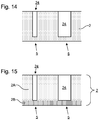
- Figures 14 and 15 show schematically a portion of a membrane 2 in which fluidic passages 24 having different aspect ratios have been formed, each of these fluidic passages 24 thereby having different fluidic resistances relative to each other.
- the left fluidic passage 24 in this particular example had a diameter of 50nm and the right a diameter of 100nm.
- the fluidic passages 24 were formed in a 300nm thick SiNx membrane 2.
- the thickness of the membrane 2 at the end of the fluidic passages 24 was 10nm. It was found that applying 10V across the membrane 2 caused a single aperture 20 to be formed in each of the two fluidic passages 24.
- Providing a fluidic passage 24 having a large enough aspect ratio to provide a functionally significant fluidic electrical resistance may require a thicker membrane 2 than is required in embodiments with shallower recesses 4 (e.g. as in Figures 4 and 5 ).
- a 300nm membrane 2 formed from SiNx was used, with fluidic passages 24 formed lithographically.
- the etch process needs to be stopped at the appropriate point to ensure the thickness of the membrane 2 at the end of the fluidic passages 24 is as required.
- small thicknesses e.g. 10nm
- the use of a membrane 2 formed from multiple layers of different compositions can be used more generally to achieve accurate thicknesses of target regions 5, recesses 4 and/or fluidic passages 24 of any form, due to different etching rates of the individual layers. Interfaces between layers of different compositions, which correspond to sudden changes or stopping of an etching process when the interfaces are reached, can be used to define any boundaries of structures formed in the membrane 2 (e.g. bottoms of recesses 4 or ends of fluidic passages 24).
- the membrane 2 comprises a first layer (e.g. the upper layer 2A in Figure 15 ) and a second layer (e.g.
- atomic layer deposition allows very uniform and precise thickness control at resolutions of the order of ⁇ 1 ⁇ .
- Materials which are inert to many reactive ion etch (RIE) processes can be applied using atomic layer deposition.
- the level of control provided by atomic layer deposition is higher than can be achieved typically using alternative film growth techniques.
- the length of the aperture which is dictated by the thickness of the layer or layers in which the aperture is formed (e.g. the lower layer 2B in Figure 15 ), can be controlled with high accuracy. More details about example configurations for the second layer (e.g. materials and sub-layers) are given below.
- fluidic passages 24 are provided using a porous layer which comprises pores that allow the ionic solution to pass from one side of the porous layer to the other side of the porous layer.
- the pores in this case are fluidic passages.
- This approach is a convenient way of providing fluidic passages 24 of high aspect ratio, due to the naturally narrow form adopted by pores in many porous materials.
- apertures 20 may be formed at the end of every pore of the porous layer that is traversed by the ionic solution. This may be desirable where the spatial distribution of the pores is suitable. However, in many cases it may be desired to form apertures 20 that are spaced apart differently (e.g. further apart), and/or are provided in different numbers (e.g.
- the porous layer may be provided in combination with a layer which comprises other fluidic passages 24 which define where the apertures 20 will be formed.
- the porous layer may provide a plurality of fluidic passages 24 which are fluidically in parallel with each other but in series with a further fluidic passage 24 provided in a separate layer which defines where the aperture 20 will be formed.
- the fluidic passage 24 in the separate layer will therefore have an opening which provides access to a plurality of the fluidic passages 24 provided by the porous layer.
- the porous layer may comprise a layer of anodized aluminium oxide (AAO).
- AAO can be formed with very high aspect ratio pores (e.g. greater than 1000:1), spaced apart in a lattice with a lattice constant of several hundred nanometres. The pore diameter and lattice constant can be tuned by forming the AAO on a suitably pre-patterned surface.
- fluidic passages 24 acting as current limiting resistors may be formed as channels within a layer of PDMS, oxide, and/or nitride.
- Embodiments have been described which allow membranes 2 to be formed which comprise a plurality of target regions 5 in each of which an aperture 20 is formed.
- Each target region 5 comprises a recess 4 or a fluidic passage 24 defining where the aperture 20 will be formed.
- Each aperture 20 is located within a different one of the target regions 5 and has a diameter determined by the resistance of any limiting resistor, the voltage regime applied and/or the thickness of the target region 5.
- the diameter may be equal to or greater than a minimum thickness of the membrane material separating the first and second baths where thickness is used as a primary means to control the diameter. Alternatively the diameter can be made smaller than the thickness of the membrane material.
- Figures 16-19 depict steps in an example method of manufacturing a membrane assembly 36 in which atomic layer deposition is used to form a membrane 2.
- the membrane 2 is suitable for allowing formation of one or more apertures using dielectric breakdown according to any of the embodiments described herein.
- Figure 16 shows an arrangement which may be formed in the same way as the membrane assembly 36 described above with reference to Figure 1 , except that the arrangement of Figure 16 does not yet have any recesses 4 formed in a membrane.
- the upper covering layer 51 in Figure 16 may be formed in the same way as the membrane 2 of Figure 1 (e.g. from SiNx).
- the lower covering layer 52 of Figure 16 may be formed in the same way as layer 10 in Figure 1 (e.g. from SiNx).
- Atomic layer deposition is used to deposit an ALD layer 54 to provide the arrangement shown in Figure 17 .
- Atomic layer deposition which may be referred to as ALD, is a known technique for depositing thin films of material. The following is one example of a review paper on this topic: Steven M. George, "Atomic Layer Deposition: An Overview", Chem. Rev. 2010, 110, 111-131 .
- a fluidic passage 24 is formed in the upper covering layer 51, for example by lithography followed by a reactive ion etch.
- the fluidic passage 24 may be formed, for example, by etching through the upper covering layer 51 to the interface between the upper covering layer 51 and the ALD layer 54.
- the membrane assembly 36 shown in Figure 18 is thereby provided.
- the ALD layer 54 could be deposited at an earlier stage, for example prior to processing of a wafer to form the layer 8 (e.g. by KOH etching to selectively remove portions of the wafer to form the layer 8, which make the structure more fragile) and/or prior to growth of the upper covering layer 51 (e.g. SiNx).
- the ALD layer 54 may even be sandwiched between two layers forming all or part of the upper covering layer 51 (e.g. between two SiNx layers).
- Forming the ALD layer 54 earlier may desirably reduce the number of processing steps that need to be carried out while the membrane assembly is in a relatively fragile state (e.g. while thin membranes are present and/or after a wafer has been processed to form the layer 8).
- the membrane assemblies 36 shown in Figures 18 and 19 are examples in which a membrane 2 comprises a first layer (the upper covering layer 51 in Figures 18 and 19 ) and a second layer (the ALD layer 54 in Figures 18 and 19 ), and the second layer is formed by atomic layer deposition.
- the plurality of sub-layers 61,62 comprises a sequence of sub-layers 61,62 that repeats a plurality of times, each repeating sequence comprising at least a first sub-layer 61 and a second sub-layer 62 directly adjacent to the first sub-layer 61.
- the first sub-layers 61 have a different composition to the second sub-layers 62.
- each unit of the repeating sequence consists of a single first sub-layer 61 and a single second sub-layer 62 but this is not essential.
- each repeating unit may comprise more than two sub-layers (e.g. three sub-layers, four sub-layers, or more).
- all of the first sub-layers 61 have the same composition as each other and all of the second sub-layers 62 have the same composition as each other.
- a repeating sequence comprising four units, each consisting of a first sub-layer 61 and a second sub-layer 62 is shown for ease of depiction (with an additional first sub-layer 61 being provided so that the two outermost surfaces of the plurality of sub-layers have the same composition). In practice a larger number of sub-layers will normally be provided.
- each of the first and second sub-layers 61,62 is formed using four or fewer cycles of atomic layer deposition, for example one cycle, two cycles, three cycles, or four cycles.
- each of one or both of the first and second sub-layers 61,62 can be formed using more than four cycles of atomic layer deposition.
- Each of the first and second sub-layers 61,62 will typically have a thickness of the order of ⁇ 1 ⁇ per cycle of atomic layer deposition used to create them.
- the number of first and second sub-layers 61,62 (and any other sub-layers that are provided) is chosen to provide a desired overall thickness for the plurality of sub-layers.
- the thickness of the plurality of sub-layers 61,62 defines the length of any aperture formed through the plurality of sub-layers 61,62.
- the thickness of the plurality of sub-layers 61,62 is in the range of 2-6nm, optionally 2-4nm, optionally 2-3nm. In an embodiment, about 20-60 cycles of atomic layer deposition are used to form the plurality of sub-layers 61,62.
- the first sub-layers 61 are non-epitaxial with respect to the second sub-layers 62. Arranging for the first sub-layers 61 to be non-epitaxial with respect to the second sub-layers 62 reduces the formation of defects due to crystal growth within the sub-layers 61,62, preserving an amorphous film. Where the plurality of sub-layers comprises other sub-layers, it is preferably arranged that all sub-layers are non-epitaxial with respect to any directly adjacent sub-layers.
- the first sub-layers 61 and the second sub-layers 62 can be formed from a wide range of different materials.
- the first sub-layers 61 comprise HfO 2 and the second sub-layers 62 comprise Al 2 O 3 .
- HfO 2 has good dielectric properties. These two materials are compatible with atomic layer deposition and are non-epitaxial with respect to each other.
- the removal of the protective layer 63 will result in a repeating sequence of sub-layers 61,62 and an additional layer, such that the two outermost sub-layers are both first sub-layers 61 (as shown in Figures 20 and 21 ).
- An aperture is subsequently formed by dielectric breakdown through the freestanding membrane.
- one or more of the apertures 20 formed using the methods and apparatus discussed above, or according to other embodiments are used to sense a molecular entity by performing a measurement (e.g. an electrical measurement or an optical measurement) that is dependent on an interaction between the molecular entity and the aperture.
- a sensing apparatus is provided having a plurality of the apertures 20 thus formed and a measurement system configured to sense a molecular entity in each of the apertures 20 by performing a measurement that is dependent on an interaction between the molecular entity and the aperture 20.
- Sensing of molecular entities can provide the basis for identifying single molecules and molecular entities. There are a wide range of possible applications, such as sequencing of DNA or other nucleic acids; sensing of chemical or biological molecules for security and defence; detection of biological markers for diagnostics; ion channel screening for drug development; and label free analysis of interactions between biological molecules.
- the polynucleotide may be labelled with one of more of a fluorescent label, an optical label, a magnetic species or a chemical species, wherein detection of the species or label is indicative of the polynucleotide.
- Nucleic acid probes may be hybridised to the polynucleotide and resultant structure detected by translocation through an aperture of the array, such as disclosed in published application WO2007/041621 .
- the polynucleotide may be labelled with one or more acceptor labels, which interact with one or more donor labels attached to an aperture of the array, such as disclosed by published application WO2011/040996 .
- the polynucleotide may be any synthetic nucleic acid known in the art.
- the molecular entity may be an aptamer. The molecular entity is caused to translocate the aperture and the interactions between the molecular entity and the aperture measured.
- the solid state membrane may comprise either or both of organic and inorganic materials, including, but not limited to, microelectronic materials, whether electrically conducting, electrically semiconducting, or electrically insulating, including materials such as II-IV and III-V materials, oxides and nitrides, such as silicon nitride, Al 2 O 3 , and SiO 2 , Si, MoS 2 , solid state organic and inorganic polymers such as polyamide, plastics such as Teflon®, or elastomers such as two-component addition-cure silicone rubber, and glasses.
- a membrane may be formed from monatomic layers, such as graphene, or layers that are only a few atoms thick such as those disclosed in U.S. Patent No.
- a biological nanopore may be provided within a solid state aperture.
- a biological nanopore may be provided within a solid state aperture.
- the measurement may for example be electrical, optical or both.
- the electrical measurement may comprise measurement of ion flow through the apertures under a potential difference or concentration gradient. Electrical measurements may be made using standard single channel recording equipment as described in Stoddart D et al., Proc Natl Acad Sci, 12;106(19):7702-7 , Lieberman KR et al, J Am Chem Soc. 2010;132(50):17961-72 , and International Application WO-2000/28312 . Alternatively, electrical measurements may be made using a multi-channel system, for example as described in International Application WO-2009/077734 and International Application WO-2011/067559 . Optical measurements may be combined with electrical measurements ( Soni GV et al., Rev Sci Instrum. 2010 Jan;81(1):014301 ).
- the sensing apparatus may comprise a measurement system arranged as disclosed in any of WO-2008/102210 , WO-2009/07734 , WO-2010/122293 , WO-2011/067559 or WO2014/04443 .
- the sensing apparatus may comprise electrodes arranged on each side of the membrane in order to measure an ion current through an aperture under a potential difference.
- the electrodes may be connected to an electrical circuit which includes a control circuit arranged to supply a voltage to the electrodes and a measurement circuit. arranged to measure the ion flow.
- a common electrode may be provided to measure ion flow through the apertures between the common electrode and electrodes provided on the opposite side of the membrane.
- one or more polymer units may be present in the pore at any particular time and the measurement carried out may be dependent on a group of k polymer units, where k is an integer.
- a group of k polymer units where k is greater than one may be referred to as a k-mer.
- this might be thought of as the measurement system having a "blunt reader head" that is bigger than the polymer unit being measured.
- Determination of a sequence characteristic of k polymer units involving the measurement of k-mers may be carried out by methods disclosed by International Patent Applications PCT/GB2012/052343 and PCT/GB2013/050381 .
- determination of sequence information or molecular sequence classification may be carried out using an artificial neural network (ANN).
- ANN artificial neural network
- the voltage used is preferably in a range having a lower limit selected from -400 mV, -300 mV, -200 mV, -150 mV, -100 mV, -50 mV, -20mV and 0 mV and an upper limit independently selected from +10 mV, + 20 mV, +50 mV, +100 mV, +150 mV, +200 mV, +300 mV and +400 mV.
- the voltage used is more preferably in the range 100mV to 2V. It is possible to increase discrimination between different nucleotides by an aperture by using an increased applied potential.
- measurement of a conductance or resistance may be carried out.
- Alternative or additional measurements associated with movement of the molecular entity with respect to the aperture may be carried out, such as measurement of a tunnelling current across the aperture ( Ivanov AP et al., Nano Lett. 2011 Jan 12;11(1):279-85 ), or a field effect transistor (FET) device, such as disclosed by WO 2005/124888 , US8828138 , WO 2009/035647 , or Xie et al, Nat Nanotechnol. 2011 Dec 11; 7(2): 119-125 .
- the measurement device may be an FET nanopore device comprising source and drain electrodes to determine the presence or passage of a molecular entity in the apertures.
Landscapes
- Chemical & Material Sciences (AREA)
- Engineering & Computer Science (AREA)
- Chemical Kinetics & Catalysis (AREA)
- Life Sciences & Earth Sciences (AREA)
- Health & Medical Sciences (AREA)
- Organic Chemistry (AREA)
- Physics & Mathematics (AREA)
- Electrochemistry (AREA)
- Materials Engineering (AREA)
- Metallurgy (AREA)
- Biomedical Technology (AREA)
- Proteomics, Peptides & Aminoacids (AREA)
- Biochemistry (AREA)
- Immunology (AREA)
- Molecular Biology (AREA)
- Analytical Chemistry (AREA)
- Biophysics (AREA)
- General Health & Medical Sciences (AREA)
- Manufacturing & Machinery (AREA)
- Inorganic Chemistry (AREA)
- Optics & Photonics (AREA)
- Zoology (AREA)
- Wood Science & Technology (AREA)
- Spectroscopy & Molecular Physics (AREA)
- Hematology (AREA)
- General Physics & Mathematics (AREA)
- Medicinal Chemistry (AREA)
- Food Science & Technology (AREA)
- Nanotechnology (AREA)
- Pathology (AREA)
- Urology & Nephrology (AREA)
- Microbiology (AREA)
- Biotechnology (AREA)
- Bioinformatics & Cheminformatics (AREA)
- General Engineering & Computer Science (AREA)
- Genetics & Genomics (AREA)
- Physical Or Chemical Processes And Apparatus (AREA)
- Micromachines (AREA)
- Separation Using Semi-Permeable Membranes (AREA)
- Semiconductor Integrated Circuits (AREA)
Description
- The invention relates to a method and apparatus for forming single or multiple apertures in a solid state membrane using dielectric breakdown. The apertures may be nanoscale apertures, which may be referred to as nanopores, each having dimensions at the nanometre scale, for example a length and/or diameter of less than about 100 nm. The resultant porous membrane may be used in a wide number of applications.
- Nanopores may be used in various devices where operations at the nanoscale are required. One important application is in localising, detecting and/or characterising molecules such as polynucleotides or polypeptides. Nanopore filters and nanoscale porous membranes are likewise important for many critical biological separation and characterization procedures, as well as filtration processes. Many other microfluidic and nano-fluidic processing and control applications similarly rely on nanoscale features in nanometric materials.
- To produce a nanoscale structure such as a nanopore in a nanometrically-thin material, it is in general required to manipulate with the precision of single atoms. This is in contrast to most conventional microelectronic fabrication processes, which characteristically only require precision down to 10s of nanometres. Without feature resolution and fabrication precision at the atomic level, it is challenging to manipulate nanometrically-thin materials in a manner that exploits the particular characteristics which emerge at the nanoscale. Numerous methods for preparing nanopores in solid state membranes have been proposed, such as for example the methods disclosed in
WO03003446 A3 - High precision nanoscale processing has historically required a one-at-a-time fabrication paradigm that is often costly and inefficient. Generally, the high-volume, batch fabrication techniques of conventional microelectronic production have been incompatible with nanoscale feature production and material manipulation. This has impeded commercial implementation of many important nanoscale applications.
- Dielectric breakdown has been explored as an alternative approach for forming nanoscale apertures. However, controlling the dielectric process has been found to be challenging. Individual electronic control of the breakdown process for each aperture was found to be necessary to avoid damage to the membrane in which the apertures were formed and/or to achieve a desired aperture size. Forming apertures in thicker membranes was difficult because larger voltages were necessary. Larger voltages increase the risk of damage to the membrane or the formation of irregular apertures. Apertures of a precise desired size between a given solution chamber could only be produced one at a time, unless complex microfluidic arrangements were provided for forming multiple, mutually isolated fluid chambers at different positions, limiting the possibilities of commercial application.
- It is an object of the invention to provide methods and apparatus which allow single or multiple apertures to be formed quickly and cheaply in a solid state membrane, particularly at the nanoscale.
- According to an aspect of the invention, there is provided a method according to
claim 1 of forming a plurality of apertures in a solid state membrane using dielectric breakdown, wherein the membrane comprises a first surface area portion on one side of the membrane and a second surface area portion on the other side of the membrane, and each of a plurality of target regions comprises a recess or fluidic passage in the membrane that opens out into the first or second surface area portion, the method comprising: contacting all of the first surface area portion of the membrane with a first bath comprising ionic solution and all of the second surface area portion with a second bath comprising ionic solution; and applying a voltage across the membrane via first and second electrodes in respective contact with the first and second baths comprising ionic solutions to form an aperture at each of a plurality of the target regions in the membrane. The first and second baths may comprise different ions from each other. The ionic strength of the two baths may differ. As an alternative to the provision of an ionic solution, the first and/or second bath may comprise an ionic liquid. - Thus, a method is provided in which multiple apertures can be formed in parallel using dielectric breakdown. In an embodiment, at least 10 apertures are formed in parallel, optionally at least 50, optionally at least 100, optionally at least 1000, optionally at least 10000, optionally at least 100000, optionally at least 1000000. A continuous body of the ionic solution is brought into contact simultaneously with a plurality of target regions. The electrodes allow a potential difference to be applied across all of the target regions simultaneously. Dielectric breakdown and the formation of apertures occurs in parallel, thereby allowing a large number of apertures to be formed in the same amount of time as would be required for a single aperture. A large number of apertures can therefore be produced efficiently.
- In an embodiment the method is applied in such a way that a single aperture is formed in each of the target regions. This may be achieved for example using suitably shaped and/or dimensioned and/or spatially distributed recesses or fluidic passages. For example, the apparatus may be arranged so that when dielectric breakdown occurs in one of the target regions the resulting reduction in electrical resistance through the membrane in the target region (due to the new electrical path provided by the aperture) does not prevent dielectric breakdown occurring in neighbouring target regions (e.g. by positioning the neighbouring target regions sufficiently far away).
- Each of the target regions comprises a region where the thickness of membrane material separating the first bath from the second bath is thinner than elsewhere (so as to favour dielectric breakdown in that particular region relative to other regions). Where this thinning is provided by a recess or fluidic passage, the average depth of the recess or fluidic passage will typically be at least 10% less and may be at least 20%, 30%, 40%, 50%, 60%, 70%, 80%, 90%, 95% or 99% less than an average thickness of the membrane in regions where recesses or fluidic passages are not present. In one particular embodiment the thickness in the recess or fluidic passage is about 5-6nm and the thickness in regions outside of the recess or fluidic passage is about 50-60nm. In other embodiments the thickness in the recess or fluidic passage may be as small as about 2-3nm. In an embodiment a fluidic passage is formed in a membrane having a thickness of more than 300nm. Arranging for the thickness in a recess or fluidic passage to be about 2-3nm in such an embodiment would result in an average depth in the recess or fluidic passage being at least 99% less than an average thickness of the membrane in regions where recesses or fluidic passages are not present.
- In an embodiment, the aperture in each target region is grown until a diameter of the aperture is equal to or greater than a minimum thickness of membrane material separating the first bath from the second bath in the target region. The minimum thickness may be the thickness at the bottom of a recess or the thickness at the end of a fluidic passage. The inventors have recognised that a rate of growth of the aperture reduces suddenly when the diameter of the aperture is equal to or slightly greater than a thickness of membrane material (typically between about 1 and 1.5 times the thickness of the membrane material) in which the aperture is being formed. This is because the access resistance becomes significant when the aperture diameter is comparable to the aperture thickness, which results in the voltage drop across the aperture being reduced. In other words, the access resistance acts as a limiting resistor. By deliberately growing the aperture until this point is reached it is possible to control the diameter of the aperture accurately without sophisticated electronics. In particular, it is possible simultaneously to form multiple apertures of the same size, even where those apertures may have started growing at slightly different times and/or have undergone slightly different growth rates (due to the stochastic nature of the dielectric breakdown process). When the diameters of some of the apertures become equal to or greater than the thickness of the membrane material where they are formed, the other apertures will quickly catch up, thereby leading to a highly uniform size distribution (for example such that a diameter variation between different pores is within about 10-20% or better). This approach, based on using the thickness of the membrane material to control aperture size, allows accurate control of aperture size because modern fabrication processes can control the thickness of the membrane material (i.e. during formation of the recesses or fluidic passages) with high accuracy. For example thickness accuracy down to 1nm or even sub nm is realistic, whereas the accuracy with which features can be formed in directions perpendicular to the depth using standard lithographic processes is typically of the order of 10s of nm.
- The diameter of the apertures that may be produced using the method of the invention may range from 0.1nm to 100nm, such as from 1.0nm to 10nm. Apertures of 0.5nm, 0.6nm, 0.7nm, 0.8nm, 0.9nm, 1.5nm, 2nm, 3nm, 4nm or 5nm may be produced. The distance (pitch) between the apertures may be 10nm or more, optionally 50nm or more, optionally 100nm or more, optionally 1 micron or more, optionally 50 microns or more depending upon the application. The apertures may be provided in a regular array, for example a square or hexagonal packed array, or an irregular array. For example, a square packed array with apertures having a diameter of 2nm and a separation between the apertures of 20nm, the density of the apertures in the array is 1/121nm2.
- In an embodiment, the thickness of the membrane material at the bottom of recesses or at the end of fluidic passages is controlled by forming the membrane from a plurality of different layers (e.g. two layers) and using the interface between two of the layers to define a boundary of the recess or fluidic passage (e.g. the bottom or end, respectively), e.g. by arranging for an etching process to slow down or stop at or near (e.g. just beyond) the interface. Arranging for the etching process to slow down or stop at or near the interface can be achieved by selecting the compositions of the layers and the nature of the etching process (e.g. etchant composition) such that the etching process proceeds quickly for one of the layers and slowly or not at all for the other layer.
- In an embodiment one or more of the target regions comprises a fluidic passage and one or more of the fluidic passages has an aspect ratio of greater than 1, optionally greater than 5, optionally greater than 10, optionally greater than 20, optionally greater than 30, optionally greater than 40, optionally greater than 50, optionally greater than 75, optionally greater than 100. The aspect ratio is defined as a ratio of a length of the fluidic passage to an average width of the fluidic passage. Fluidic passages having a high aspect ratio will typically have a fluidic electrical resistance that is higher than fluidic passages having a lower aspect ratio. Such fluidic passages can act as current limiting resistors, reducing the voltage across the membrane significantly when the aperture is formed. The voltage will be reduced by approximately R2/(R1 + R2) where R2 is the resistance of the fluidic passage, and R1 is the resistance of the aperture. This expression does not take into account the effects of access resistance or fully account for regions where the electrical field lines change direction. A more accurate description of the voltage reduction, with access resistance included, is given by the following expression:

- In an embodiment, one or more of the target regions comprises a fluidic passage and in each of one or more of the fluidic passages an aperture is formed which has a fluidic electrical resistance of less than 10 times the fluidic electrical resistance of the fluidic passage, optionally less than 5 times, optionally less than 2 times. In an embodiment, one or more of the target regions comprises a fluidic passage and in each of one or more of the fluidic passages an aperture is formed which has a fluidic electrical resistance that is less than the fluidic electrical resistance of the fluidic passage. Arranging for the fluidic electrical resistance of a fluidic passage to be a least a significant portion (e.g. between about 0.3 and 0.5) of the fluidic electrical resistance of the aperture in this manner ensures that after aperture formation there is a significant voltage drop along the length of the fluidic resistor, reducing the voltage drop across the membrane material in the region of the aperture. Furthermore, providing fluidic passages having a significant fluidic electrical resistance reduces the effect of the formation of an aperture in one fluidic passage on the electrical field in any neighbouring fluidic passage. Even in a case where an erroneously large aperture is formed in one fluidic passage, the fluidic electrical resistance of the fluidic passage itself will prevent any excessive reduction in the electrical field in neighbouring fluidic passages, such that apertures can still be correctly formed in those passages.
- In an embodiment, fluidic passages having different fluidic electrical resistances are provided in different target regions, and a corresponding plurality of differently sized apertures are grown in parallel via the voltage applied via the first and second electrodes. This allows efficient formation of multiple apertures of different size in a controlled manner. In this embodiment, the reduction in voltage across the aperture after the aperture has been formed will be different for each of the fluidic passages having a different fluidic electrical resistance. The subsequent rate of growth of the apertures will thus be different. This can be exploited to enable simultaneous formation of apertures of different size, even if the thickness of the membrane material at the end of the fluidic passages is the same. The size of aperture at which the rate of growth slows markedly will be different for each of the fluidic passages having a different fluidic electrical resistance.
- In an aspect of the disclosure, there is provided a method of forming an aperture in a solid state membrane using dielectric breakdown, wherein the membrane comprises a first surface area portion on one side of the membrane and a second surface area portion on the other side of the membrane, comprising: contacting the first surface area portion of the membrane with a first bath comprising ionic solution and the second surface area portion with a second bath comprising ionic solution; and applying a voltage across the membrane via first and second electrodes in respective contact with the first and second baths comprising ionic solutions to form an aperture in the membrane, wherein a current limiting resistor is provided in series between the membrane and the first or second electrode, the current limiting resistor having an electrical resistances which is at least 10% as high as an electrical resistance of the aperture at any time after formation of the aperture, optionally at least 20%, optionally at least 50%, optionally at least 100%.
- The current limiting resistor provides a resistance that is in addition to the access resistance associated with the ionic solutions in the first and second baths when the current limiting resistor is not present. The current limiting resistor increases an amount of reduction of voltage across the aperture when the aperture is formed, relative to a case where the current limiting resistor is not provided. The current limiting resistor may comprise either or both of a fluidic resistor provided in the first or second bath and an external resistor that is provided at least partially outside of the first and second baths. The external resistor may be a conventional resistor of the passive solid state type which is routinely used in electrical circuits not involving fluids.
- The current limiting resistor provides a simple way of controlling the rate of the aperture diameter growth process without sophisticated and expensive electronics. The current limiting resistor determines the eventual aperture diameter at a given applied voltage. The approach is simpler for example than prior art alternatives in which electronic feedback is used to cut off the voltage when dielectric breakdown begins, or in which very short voltage pulses are used to allow the voltage to be stopped quickly enough. The method may nonetheless comprise the use of electronic feedback to indicate the formation of the apertures, for example by measurement of the change in ion current flowing through the apertures between the electrodes. The feedback may be operative for example to limit the number of apertures formed, for example by switching off the dielectric breakdown process after a particular value of ion current has been exceeded.
- In an alternative aspect, there is provided a method of forming an aperture in a solid state membrane using dielectric breakdown, the method comprising: applying a voltage across the membrane to form the aperture using dielectric breakdown, wherein: the membrane comprises a plurality of sub-layers; at least two of the sub-layers have a different composition relative to each other; and each of the sub-layers is formed by atomic layer deposition.
- The inventors have found that forming the membrane from multiple sub-layers of different composition using atomic layer deposition makes it possible to control the geometry of apertures with high accuracy, even where the membrane is extremely thin. Atomic layer deposition allows very uniform and precise thickness control at resolutions of the order of ∼1Å. Materials which are inert to many reactive ion etch (RIE) processes can be applied using atomic layer deposition. The level of control provided by atomic layer deposition is higher than can be achieved typically using alternative film growth techniques. The length of the aperture, which is dictated by the thickness of the layer or layers in which the aperture is formed, can be controlled with high accuracy.
- Where the aperture is used for sensing a molecular entity (e.g. DNA material) passing through the aperture, performance (e.g. the ability to distinguish between different DNA bases) has been found to depend critically on the diameter and length of the aperture. Improving the accuracy with which the diameter and/or length can be controlled improves performance.
- The inventors have furthermore found that forming the membrane from multiple sub-layers of different composition using atomic layer deposition provides an aperture that is highly stable during use. For example, the diameters and lengths of apertures formed in this way have been found to remain stable over long periods of time (e.g. several weeks or over a month) during use. In an embodiment, the plurality of sub-layers comprises a sequence of sub-layers that repeats a plurality of times, each repeating sequence comprising at least a first sub-layer and a second sub-layer directly adjacent to the first sub-layer, preferably with the first sub-layers being non-epitaxial with respect to the second sub-layers. The use of such a repeating sequence of non-epitaxial sub-layers reduces the formation of defects due to crystal growth within the sub-layers, preserving an amorphous film. The quality of the sub-layers, and the quality and integrity of the overall membrane, is thereby improved, by improving uniformity and/or reducing defect concentration.
- In an embodiment, the plurality of sub-layers is annealed prior to formation of the aperture. The anneal may be performed below a temperature at which significant crystallization in the sub-layers might occur. Alternatively, the anneal may be performed at higher temperatures. The anneal improves the quality of the sub-layers (e.g. improving uniformity and/or reducing defect concentration).
- Improving the quality of the sub-layers reduces electrical leakage through the sub-layers, which could otherwise disrupt optimal formation of apertures using dielectric breakdown.
- In an alternative aspect, there is provided an apparatus for forming a plurality of apertures in a solid state membrane using dielectric breakdown, comprising: a first bath configured to hold an ionic solution in contact with all of a first surface area portion on one side of a solid state membrane; a second bath configured to hold an ionic solution in contact with all of a second surface area portion on the other side of the membrane; and a voltage applicator comprising a first electrode configured to contact the ionic solution in the first bath and a second electrode configured to contact the ionic solution in the second bath, wherein the membrane comprises a plurality of target regions, each target region comprising a recess or fluidic passage in the membrane that opens out into the first or second surface area portion; and the target regions are configured such that a voltage applied via the first and second electrodes can cause formation of a single aperture in each of the target regions.
- In an alternative aspect, there is provided an apparatus for forming an aperture in a solid state membrane using dielectric breakdown, comprising: a first bath holding an ionic solution in contact with a first surface area portion on one side of a solid state membrane; a second bath holding an ionic solution in contact with a second surface area portion on the other side of the membrane; and a voltage applicator comprising a first electrode configured to contact the ionic solution in the first bath and a second electrode configured to contact the ionic solution in the second bath, wherein a current limiting resistor is provided in series between the membrane and the first or second electrode, the current limiting resistor having an electrical resistance which is at least 10% as high as an electrical resistance of the aperture at any time after formation of the aperture.
- In an alternative aspect, there is provided an apparatus for forming an aperture in a solid state membrane using dielectric breakdown, comprising: a bath system for holding an ionic solution in contact with each side of the solid state membrane; and a voltage applicator for applying a voltage across the membrane via the ionic solution in order to form the aperture in the membrane using dielectric breakdown, wherein: the membrane comprises a plurality of sub-layers; at least two of the sub-layers have a different composition relative to each other; and each of the sub-layers is formed by atomic layer deposition.
- In an alternative aspect, there is provided a solid state membrane comprising a plurality of apertures, each aperture having a diameter equal to or greater than a minimum thickness of membrane material separating the first bath from the second bath where the aperture is formed.
- In an alternative aspect, there is provided a solid state membrane comprising: a plurality of target regions, each target region comprising a recess or fluidic passage in the membrane; and a plurality of nanoscale apertures, each aperture being located within a different one of the target regions and having a diameter that is equal to or greater than a minimum thickness of the target region.
- Embodiments of the invention will now be described, by way of example only, with reference to the accompanying drawings in which corresponding reference symbols indicate corresponding parts, and in which:
-
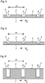
Figure 1 is a schematic side sectional view of a portion of a membrane assembly comprising a membrane with a plurality of recesses in corresponding target regions; -
Figure 2 is a magnified side sectional view of one of the recesses in the membrane ofFigure 1 , having a rectangular depth profile; -
Figure 3 is a magnified side sectional view of an alternative recess having a curved depth profile; -
Figure 4 is a magnified side sectional view of an embodiment in which the membrane comprises a plurality of recesses having rectangular depth profiles; -
Figure 5 is a magnified side sectional view of an embodiment in which the membrane comprises a plurality of recesses having curved depth profiles; -
Figure 6 is a magnified side sectional view of an embodiment in which the membrane comprises a plurality of fluidic passages having an aspect ratio greater than 1; -
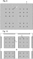
Figure 7 is a top plan view of a portion of an example membrane showing a plurality of target regions formed in a first surface area portion to be contacted by an ionic solution; -
Figure 8 is a bottom plan view of a portion of the membrane ofFigure 7 , showing a second surface area portion to be contacted by an ionic solution, each isolated region of the second surface area portion containing a single target region; -
Figure 9 is a top plan view of a portion of an alternative example membrane showing a plurality of target regions formed in a first surface area portion to be contacted by an ionic solution; -
Figure 10 is a bottom plan view of a portion of the membrane ofFigure 9 , showing a second surface area portion to be contacted by an ionic solution, each isolated region of the second surface area portion containing plural target regions; -
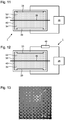
Figure 11 depicts an example apparatus for forming a plurality of nanoscale apertures; -
Figure 12 depicts an alternative example apparatus for forming a nanoscale aperture in which an external resistor is provided as a current limiting resistor; -
Figure 13 is a TEM image of an example aperture; -
Figure 14 shows a membrane comprising fluidic passages having different fluidic resistances; -
Figure 15 shows a membrane having a layered structure to facilitate accurate formation of fluidic passages; -
Figures 16-19 are schematic side sectional views depicting stages in a method of manufacturing two example membrane assemblies, depicted respectively inFigures 18 and19 ; -
Figure 20 is a schematic side sectional view of a portion of a membrane comprising a repeating sequence of sub-layers, and protective layers; -
Figure 21 is a schematic side sectional view of a portion of a membrane comprising a repeating sequence of sub-layers. - In an embodiment, an example of which is shown in
Figure 11 , there is provided anapparatus 1 for forming a plurality of apertures in a membrane. The apertures are formed by dielectric breakdown of the membrane. In an embodiment the membrane is a solid state membrane. In an embodiment the apertures are nanoscale apertures, for example apertures having a characteristic dimension (e.g. diameter or depth or both) of the order of 100nm or less, optionally 50nm or less, optionally 20nm or less, optionally 10nm or less, optionally 5nm or less, optionally 2nm or less, optionally 1nm or less. Each aperture provides a conduit extending from one side of the membrane to the other side of the membrane, thereby fully traversing the membrane. -
Figure 1 depicts an example configuration for themembrane 2. In this embodiment themembrane 2 is attached to asupport structure membrane 2 andsupport structure membrane assembly 36. Themembrane assembly 36 may be formed by manufacturing a plurality of membrane assemblies using a single integral membrane 2 (e.g. a wafer) and cutting out themembrane assembly 36 from the plurality of membrane assemblies. Alternatively, the plurality of membrane assemblies may remain connected together with theapparatus 1 being configured to interact with just one of the membrane assemblies. In such an embodiment, other instances of theapparatus 1 may be provided to interact with other ones of the membrane assemblies. Alternatively, themembrane assembly 36 may comprise the whole of a wafer forming themembrane 2. - The
membrane 2 may be composed from various materials and combinations of materials. The resistivity of themembrane 2 should be sufficiently high to allow dielectric breakdown to occur. If the resistivity is anisotropic, it should be sufficiently high in the direction perpendicular to the membrane surfaces 6, 7 to allow dielectric breakdown to occur. Themembrane 2 may comprise a single layer or a plurality of different layers. Specific examples of membranes having plural layers, and their associated advantages, are discussed below with reference toFigures 16-19 . - As shown for example in
Figures 1 and11 , theapparatus 1 comprises a first bath 38 configured to hold anionic solution 32. Theionic solution 32 in the first bath 38 contacts all of a firstsurface area portion 6 on one side of the membrane 2 (the upper side of themembrane 2 in the orientation shown in the figures). Theapparatus 1 further comprises asecond bath 40 configured to hold anionic solution 34. The composition of theionic solution 34 in thesecond bath 40 may be the same as or different from the composition of theionic solution 32 in the first bath 38. Theionic solution 34 in thesecond bath 40 contacts all of a secondsurface area portion 7 on the other side of the membrane 2 (the lower side of themembrane 2 in the orientation shown in the figures). The combination of the first bath 38 and thesecond bath 40 may be referred to as a bath system. Either or both of the first and secondsurface area portions surface area portions surface area portions surface area portion 6 will therefore be applied to all of the firstsurface area portion 6. A voltage applied to ionic solution in contact with the secondsurface area portion 7 will be applied to all of the secondsurface area portion 7. - A voltage applicator is provided for applying a voltage across the
membrane 2, including intarget regions 5. The voltage is applied via theionic solution surface area portions membrane 2. The voltage applicator comprises afirst electrode 28 and asecond electrode 30. Thefirst electrode 28 is configured to contact theionic solution 32 in the first bath 38. Thesecond electrode 30 is configured to contact theionic solution 34 in thesecond bath 40. In an embodiment, the voltage applicator comprises acontroller 26 for controlling the voltage applied by the voltage applicator. - The
membrane 2 comprises a plurality of thetarget regions 5. Each of thetarget regions 5 comprises arecess 4 orfluidic passage 24. Therecess 4 orfluidic passage 24 opens out into the first or secondsurface area portion recess 4 orfluidic passage 24 provides a path of reduced thickness between the first and second baths, thereby favouring initiation of aperture formation in thetarget region 5. For example, a region of themembrane 2 at the base of arecess 4 or at the end of afluidic passage 24 may be thinner than in regions outside of thetarget region 5. - The
apparatus 1 is configured such that a voltage applied via the first andsecond electrodes single aperture 20 in each of thetarget regions 5. Thus, for example, thetarget regions 5 are spaced apart from each sufficiently that the reduction in resistance that occurs when dielectric breakdown is initiated in onetarget region 5 does not prevent dielectric breakdown from being initiated in a neighbouringtarget region 5. This is important because although the voltage is applied simultaneously to all of thetarget regions 5, the exact moment when dielectric breakdown begins may vary significantly between different target regions. The reduction in resistance will tend to reduce the magnitude of the electric field in the region of thetarget region 5. - In the example arrangement shown in
Figure 1 , themembrane 2 comprises a layer of SiNx. Themembrane 2 is supported by alayer 8 of Si and afurther layer 10 of SiNx (such that theSi layer 8 is sandwiched between the SiNx of themembrane 2 and the SiNx of the layer 10). In the example shown, theSi layer 8 has a thickness of about 300 microns. TheSiNx membrane 2 andlayer 10 each have a thickness D3 of about 40nm. Themembrane assembly 36 may be formed as follows. Conventional lithography and a KOH etch can be used to form themembrane 2 andlayers target areas 5 comprises arecess 4 opening out into an upper surface of themembrane 2. E-beam lithography and a reactive ion etch may be used to define areas (of any shape, for example circular) defining theserecesses 4 and to thin down themembrane 2 in these areas to provide the required depth ofrecess 4.Figure 2 provides a magnified view of one of therecesses 4 ofFigure 1 . The thickness D4 of themembrane 2 in therecess 4 in this example is about 10nm (meaning that the depth of therecess 4 is about 30nm). -
Figures 7 and 8 are top and bottom plan views respectively of a portion of themembrane 2 ofFigure 1 . As can be seen, the first surface area portion 6 (Figure 7 ) consists of a single area without any holes. The secondsurface area portion 7 comprises a plurality of isolated regions which are separated from each other by thelayer 8 of the support structure. The white areas shown correspond to abottom surface 22 oflayer 10 of the support structure. In this example, the isolated regions of the secondsurface area portion 7 are square with dimensions 15x15 microns. The shape of the isolated regions is determined by the particular process chosen for fabrication. KOH etch produces square shape etch pits but reactive ion etch could take any other shape, for example, circular shape (e.g. with diameter of 15 microns). - In the examples of
Figures 1 ,7 and 8 , each of the isolated regions in the secondsurface area portion 7 contains one target region 5 (comprising arecess 4 formed in the upper side of the membrane 2). In this example thetarget regions 5 are therefore spaced relatively far apart from each other (greater than about 15 microns). However, this is not essential. In other embodiments, as shown for example inFigures 9 and 10 , each of the isolated regions in the secondsurface area portion 7 containmultiple target regions 5 and/or thetarget regions 5 are otherwise positioned closer to each other than is the case inFigures 1 ,7 and 8 . Examples of a portion of amembrane 2 having a plurality of more closely spacedtarget regions 5 are shown schematically inFigures 4-6 . In such examples, thetarget regions 5 may have a diameter D1 of about 50nm and a separation D2 of about 1 micron for example. Various other dimensions and spacings may be chosen according to requirements. In an embodiment, a single isolated region is provided and the single isolated region comprises multiple target regions. - The shape in plan view of the
recesses 4 orfluidic passages 24 may take any form, for example circular. In the embodiment described with reference toFigures 1, 2 and4 , therecesses 4 have a circular shape in plan view and a rectangular depth profile (thereby forming a cylinder). In other embodiments, therecesses 4 orfluidic passages 24 may have different profiles. In one embodiment, as shown inFigures 3 and5 forrecesses 4, therecesses 4 orfluidic passages 24 have a depth profile in which the depth increases progressively from anedge 44 of an opening of therecess 4 orfluidic passage 24 towards a central region (e.g. axially central in the case of a fluidic passage 44) of therecess 4 orfluidic passage 24, prior to a formation of anyaperture 20 in therecess 4 orfluidic passage 24. The depth profile may be a smooth depth profile, for example a rounded depth profile, as shown inFigures 3 and5 . This may be formed for example by suitable control of a reactive ion etch or by using a wet etch process. Alternatively the depth profile may be angular, e.g. conical. The area of the thinnest portion of themembrane 2 in plan view in arecess 4 orfluidic passage 24 of this type is significantly smaller than the area in plan view of the whole of therecess 4 orfluidic passage 24 as defined by theedge 44, optionally at least 75% smaller, optionally at least 90% smaller, optionally at least 95% smaller. The area in which dielectric breakdown will be most favoured (i.e. the thinnest region) may therefore be smaller in such arecess 4 orfluidic passage 24 than in other embodiments, for example as in therecesses 4 shown inFigures 1, 2 and4 . The likelihood of more than one separate aperture forming in thesame recess 4 orfluidic passage 24 is therefore reduced because there is less space available for such a process to occur. The formation of an aperture in eachrecess 4 orfluidic passage 24 can therefore be simplified and/or made more reliable. For example, as described in detail above, a repeated application of first and second voltages is not necessary to form the apertures reliably. All of the apertures can for example be formed by constantly applying a voltage at a level (e.g. 10V) which is higher than a chosen percentile or an upper limit of the statistical distribution of minimum voltages required for initiating anaperture 20. - The
fluidic passages 24 may extend perpendicularly to the plane of themembrane 2 and/or in a straight line, for example forming cylindrical shapes. However, this is not essential. Afluidic passages 24 may take various other forms, having for example at least a portion which does not extend in a straight line and/or which does not extend in a direction perpendicular to the plane of themembrane 2. Serpentine shapes and shapes in which thefluidic passage 24 has a portion extending parallel to the plane of themembrane 2 can be provided for example. Such shapes may be useful where it is desired to provide afluidic passage 24 with a high aspect ratio in order to provide a high fluidic electrical resistance. - In an embodiment,
fluidic passages 24 are provided which have an aspect ratio of greater than 1, optionally much greater than 1. The aspect ratio is defined as a ratio of a length of the fluidic passage to an average width of the fluidic passage.Figure 6 shows an example of a portion of amembrane 2 corresponding to that ofFigures 4 and 5 except that a plurality offluidic passages 24 having an aspect ratio greater than 1 are provided instead of relativelyshallow recesses 4. The role offluidic passages 24 as current limiting resistors is discussed in further detail below. - In an embodiment, a voltage is applied across the
membrane 2 until a plurality ofapertures 20 have been formed which are spatially separated from each other. In an embodiment, asingle aperture 20 is formed in each and every one of thetarget regions 5. Eachaperture 20 is formed in arecess 4 orfluidic passage 24. - In an embodiment, the
aperture 20 in eachtarget region 5 is grown (by continuing to apply the voltage) until a diameter of theaperture 20 is equal to or greater than a minimum thickness of membrane material separating the first bath from the second bath in thetarget region 5. Where afluidic passage 24 is provided the minimum thickness may be the thickness of the membrane material at the end of thefluidic passage 24. This may not be equal to theoverall membrane thickness 2 for some geometries, for example geometries in which thefluidic passage 24 does not extend exclusively in a direction perpendicular to the plane of themembrane 2. Where arecess 4 is provided the minimum thickness will typically be the thickness at the base of therecess 4. - The inventors have recognised that the rate of growth of an
aperture 20 in amembrane 2 reduces as the diameter of theaperture 20 increases. The growth rate drops to almost zero when the diameter of theaperture 20 is equal to or greater than the thickness of material in which theaperture 20 is being formed. The inventors have also recognised that this effect makes it possible to control the size ofapertures 20 formed by dielectric breakdown in a simple and reliable manner. Instead of needing to formapertures 20 individually in series, with complex electronics to monitor the growth process,multiple apertures 20 can be formed simultaneously with little or no real time monitoring of the growth process. A single voltage can be applied simultaneously tomultiple target regions 5. Dielectric breakdown may be initiated at slightly different times fordifferent target regions 5, so that during thegrowth process apertures 20 of various different sizes may co-exist. However, when the growth process reaches the point where the diameters of largerindividual apertures 20 become equal to or greater than the thickness of the material around theapertures 20, growth of thoseapertures 20 will slow significantly, allowing thesmaller apertures 20 to catch up. If the process is continued until the diameters of all of theapertures 20 are equal to or greater than the thickness of the material around theapertures 20, it is found that the slowing of the growth process for thelarger apertures 20 means that all of theapertures 20 have substantially the same size. - In an embodiment, a substantially constant uninterrupted voltage is applied for a majority of a time during which the
aperture 20 is grown by the voltage. In an embodiment, applicable particularly where thetarget regions 5 compriserecesses 4 orfluid passages 24 that have a rectangular depth profile (e.g. cylindrical), a first voltage is applied that initiates aperture formation in thetarget regions 5. The first voltage may be applied for a relatively short time (e.g. 100ms for a configuration for forming 10-20nm apertures, such as that shown inFigure 1 ). A second voltage, lower than the first voltage is applied after the first voltage for a longer time (e.g. 1 min for a configuration for forming 10-20nm apertures, such as that shown inFigure 1 ). In an embodiment the second voltage is lower than would be necessary to initiate formation of apertures in the same target regions. The second voltage is applied to grow the existingapertures 20 without generating any new apertures. In one example implementation a first voltage of about 10V was used to initiate the dielectric breakdown. A second voltage of about 9V was then used to grow theapertures 20. The process was continued until the current stabilized, indicating that diameters of theapertures 20 had reached the thickness of the material surrounding theapertures 20 and their growth had slowed. - In an embodiment, the sequence of the first and second voltages is applied a plurality of times. This may be necessary to ensure that
apertures 20 are initiated in all of thetarget regions 5. The sequence of first and second voltages may be applied repeatedly until it is detected that the current across themembrane 2 is stable. The inventors found that applying this approach to the arrangement shown inFigure 1 , for example, can be used reliably to produceplural apertures 20 having a uniform diameter of 15nm. - In an embodiment, a third voltage is applied after the first and second voltages. The third voltage is equal to or higher than the first voltage (e.g. 10V). The third voltage is applied for a longer time than either or both of the first and second voltages (e.g. 3 min). The third voltage acts to homogenize (make more uniform) the aperture diameters.
- The repeated application of the first and second voltages is particularly desirable where there is a chance of more than one aperture being formed in any single one of the
target regions 5, for example in asingle recess 4 orfluidic resistor 24 in one of thetarget regions 5. This may be more likely for example where the thinnest portion of atarget region 5 extends over a relatively large area, for example inrecesses 4 having a rectangular depth profile (e.g. as inFigures 1, 2 and4 ). Forrecesses 4 having a thinnest portion representing a smaller proportion of the target region 5 (e.g. as inFigures 3 and5 ), the repeated application of the first and second voltages may not be necessary. In this situation, all of theapertures 20 may be formed by constantly applying a voltage at a level (e.g. 10V) which is higher than the minimum required for initiating anaperture 20. - In an embodiment, the
aperture 20 in eachtarget region 5 is grown until a diameter of theaperture 20 is in the range of 5nm to 40nm. However, apertures which are smaller than this range or larger than this range may also be formed according to requirements. - In an embodiment all of the
recesses 4 orfluidic resistors 24 provided have the same geometry (e.g. depth, thickness profile, length, aspect ratio, thickness etc.). This may be appropriate where it is desired simultaneously to form identical apertures in each of thetarget regions 5. - In an embodiment one or more of the
target regions 5 comprises arecess 4 having an average width less than 5 times an average depth. The inventors have found that keepingrecesses 4 within this constraint greatly reduces the risk of more than oneaperture 20 being initiated in thesame recess 4. - The above described embodiments, and other embodiments, allow
membranes 2 to be formed which comprise a plurality ofapertures 20. The aperture diameter can be controlled by the thickness of the material in which the apertures are formed, for example by growing each aperture until its diameter is equal to or greater than a thickness of the membrane material separating the two baths in the region where the aperture is formed. Modern fabrication processes allow the membrane thickness to be controlled with very high precision (e.g. down to 1nm or less), thereby allowing accurate control of the aperture diameter. It is not essential for each aperture to be grown until its diameter is equal to or greater than a thickness of themembrane 2 in the region where the aperture is formed. In other embodiments, apertures are formed that are smaller than this. - Relatively high voltages can be required to initiate the dielectric breakdown process. This is particularly the case where relatively large apertures (e.g. greater than about 30nm) need to be formed, because this requires a thicker membrane in the target regions and, consequently, a higher voltage for breakdown. The sudden reduction in resistance that occurs when the dielectric breakdown first occurs can lead to a large current flowing through the
baths aperture 20. The large current could in principle oxidise or reduce a species present in the ionic solution in the baths and/or lead to damage to, or unpredictable behaviour of, theaperture 20 itself. For example, in a 46nm thick SiNx membrane with 100nm diameter, 30nm thick recesses, an applied voltage of 20-30V is required to initiate dielectric breakdown. The current driven through the system after dielectric breakdown can completely destroy theaperture 20. - In an embodiment, an example of which is shown in
Figure 12 , a current limitingresistor 46 is provided. The current limiting resistor provides a resistance that is additional to the access resistance provided through the ionic solution in the absence of the current limitingresistor 46. The current limitingresistor 46 is provided in series between themembrane 2 and the first orsecond electrode membrane 2 suddenly falls when anaperture 20 is formed in themembrane 2, the current limitingresistor 46 limits the resulting increase in current flow through theaperture 20. The current limitingresistor 46 acts to reduce the voltage acting across theelectrodes resistor 46, thecontroller 26 will try to maintain a constant voltage between theelectrodes aperture 20 only falling in that case with increasing current due to the potential drop across the ionic solution between theelectrodes aperture 20, or because of overload of the power source being used by thecontroller 26. The current limitingresistor 46 therefore increases an amount of reduction of voltage across eachaperture 20 when theaperture 20 is formed, relative to a case where the current limitingresistor 46 is not provided. In the example discussed above (46nm thick SiNx membrane with 100nm diameter, 30nm thick recess), a current limitingresistor 46 of about 2MΩ was found to be suitable. More generally, the current limiting resistor should have an electrical resistance which is at least 10% as high as an electrical resistance of the aperture (i.e. a fluidic electrical resistance of the aperture) at any time after formation of the aperture 20 (i.e. after theaperture 20 is fully formed, rather than during an intermediate transient phase immediately after dielectric breakdown first takes place). Typically, the current limiting resistor is chosen to have an electrical resistance that is of a similar order of magnitude to the fluidic electrical resistance of theaperture 20, so that a significant drop in the potential difference across the membrane at theaperture 20 occurs when theaperture 20 is formed. - The current limiting
resistor 46 also reduces the rate of growth of theaperture 20 for a constant applied voltage. The rate of growth can be made sufficiently slow that a high level of control of diameter can be achieved simply by comparing a measured current flow with calibration data relating current to aperture size. Arrangements can be made for example for the applied voltage to be shut off when the calibration data indicates that the aperture has reached a desired size. As an illustrative example, for the 30nm thick recesses mentioned above, it was found that slow expansion over of period of about 8 minutes is effective for growing anaperture 20 from a starting diameter of about 12nm immediately after aperture formation (using a voltage of about 23V) to a final diameter of 43nm. An image of thefinal aperture 20 is shown inFigure 13 . As can be seen, theaperture 20 is accurately circular with a smooth edge. - In an embodiment, the current limiting
resistor 46 is an external resistor (e.g. a solid state resistor) positioned outside of thebaths 38,40. In other embodiments, the current limitingresistor 46 may comprise a fluidic resistor or a fluidic resistor and an external resistor. - Where a current limiting resistor is provided which provides a significant reduction in voltage across the
membrane 2 when the aperture is formed, only a single aperture can normally be formed per current limiting resistor. Thus, arrangements of the type shown inFigure 12 would normally be used to form asingle aperture 20. However, where fluidic resistors are used as current limiting resistors, more than one such current limiting resistor can be provided within a given bath comprising ionic solution. This makes it possible to form multiple apertures in parallel while also using current limiting resistors to enhance control of the process. - For example, a plurality of the
fluidic passages 24 may be configured to operate as current limiting resistors. In this case, each of one or more of thefluidic passages 24 is configured such that when anaperture 20 is formed in thefluidic passage 24 the fluidic electrical resistance of theaperture 20 is less than 10 times the fluidic electrical resistance of the fluidic passage, optionally approximately equal to the fluidic electrical resistance of thefluidic passage 24. Thefluidic passages 24 may for example be made relatively elongate. The degree of elongation of the fluidic passages may be parameterized by reference to the aspect ratio. The aspect ratio may be defined as the ratio of a length of thefluidic passage 24 to an average width of thefluidic passage 24. In the case of a cylindrical fluidic passage, the aspect ratio would simply be the ratio of the axial length of the cylinder to the diameter of the cylinder. Where thefluidic passage 24 has a more complex form, e.g. with a non-circular cross-section and/or a cross-section which varies along the length of thefluidic passage 24, an average value for width can be used. In order to provide a sufficiently high fluidic electrical resistance, the aspect ratio of thefluidic passages 24 may be greater than 1, optionally significantly higher. - An appropriate fluidic resistance of a fluidic resistor (e.g. fluidic passage 24) acting as a current limiting resistor can be achieved by appropriate design of the geometry of the fluidic resistor and selection of the resistivity of the ionic solution that will be present within the fluidic resistor. Taking for example a simple cylindrical fluidic resistor geometry, the fluidic resistance R can be expressed by the following expression:

- Taking the example above, we can estimate the requirement for an
aperture 20 formed in a 30nmthick membrane 2 of silicon nitride and ∼2MΩ limiting resistor completely defined by a cylindrical fluidic passage through a 2µm thick dielectric coating (silicon oxide) on top of themembrane 2. If it is a similar -9.1Ωcm resistivity solution on both sides, the required diameter of the fluidic resistor is approximately 340nm. This diameter and aspect ratio can be achieved by conventional lithography easily. - In some cases, when the required
aperture 20 is very small and the diameter of the fluidic resistor is limited by lithography, the required aspect ratio of the fluidic resistor can be very large. For example, a ∼2nm diameter aperture 20 in a 10nmthick membrane 2 will require 20-30µm long fluidic channel if the diameter is limited to 100nm. Increasing the resistivity of solution in the fluidic resistor (such as by diluting the solution or filling it with a gel or porous materials) can help reduce the aspect ratio requirement. Since there is no diffusion across themembrane 2 before dielectric breakdown, diluting the solution to increase the resistivity can proportionally reduce the required aspect ratio of the fluidic resistor if application of the voltage is stopped quickly after breakdown, before diffusion reaches the steady state. For example, 100 times increased resistivity of the solution in the fluidic resistor can lead to a lithography-friendly 200nm diameter and 1µm long fluidic resistor. Even in a case where the voltage is not stopped quickly enough that the diffusion does not reach the steady states, the fluidic resistance follows the following equation roughly as long as the fluidic resistor has a much larger aspect ratio than the aspect ratio of nanopore: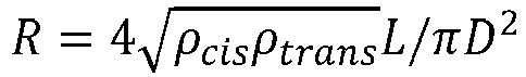
- Here ρcis and ρtrans are the bulk resistivity of solution in the cis and trans chamber respectively. According to this equation, a same 2nm diameter and 10nm thick pore only requires ∼115nm diameter and 1µm long fluidic resistor if we fill the fluidic resistor with a solution that is 1000 times more resistive.
- In the embodiments discussed above only a single current limiting resistor is provided or a plurality of identical current limiting resistors are provided (e.g. such as in
Figure 6 ). This is not essential. In other embodiments, a plurality offluidic passages 24 are provided which have different fluidic electrical resistances. Where the fluidic resistances are sufficiently large to have a significant impact on the growth rates of theapertures 20 formed in the respectivefluidic passages 24, this approach allows differentlysized apertures 20 to be grown in parallel via the voltage applied via the first and second electrodes (i.e. simultaneously across all of the target regions 5).Apertures 20 influidic passages 24 having a relatively high fluidic electrical resistance will tend to grow more slowly thanapertures 20 influidic passages 24 having a lower fluidic electrical resistance. Thus, controlled, simultaneous formation ofapertures 20 having different sizes to each other is made possible. - In an embodiment, the rate of growth of an
aperture 20 is controlled by controlling the ionic strength of the ionic solution in the first orsecond bath 38,40, which determines the fluidic resistance in afluidic passage 24 associated with theaperture 20. For example, by changing the ionic solution so that the fluidic resistance increases, it is possible to slow the rate of aperture growth and vice versa. -
Figures 14 and 15 show schematically a portion of amembrane 2 in whichfluidic passages 24 having different aspect ratios have been formed, each of thesefluidic passages 24 thereby having different fluidic resistances relative to each other. Theleft fluidic passage 24 in this particular example had a diameter of 50nm and the right a diameter of 100nm. Thefluidic passages 24 were formed in a 300nmthick SiNx membrane 2. The thickness of themembrane 2 at the end of thefluidic passages 24 was 10nm. It was found that applying 10V across themembrane 2 caused asingle aperture 20 to be formed in each of the twofluidic passages 24. The current limiting effect of thenarrower fluidic passage 24 meant that when theaperture 20 in thewider fluidic passage 24 reached a diameter equal to 10nm (the thickness of the membrane material at the end of the fluidic passage 24), theaperture 20 in thenarrower fluidic passage 24 only had a diameter of 5nm. - Providing a
fluidic passage 24 having a large enough aspect ratio to provide a functionally significant fluidic electrical resistance may require athicker membrane 2 than is required in embodiments with shallower recesses 4 (e.g. as inFigures 4 and 5 ). In the example ofFigures 14 and 15 a300nm membrane 2 formed from SiNx was used, withfluidic passages 24 formed lithographically. The etch process needs to be stopped at the appropriate point to ensure the thickness of themembrane 2 at the end of thefluidic passages 24 is as required. For small thicknesses (e.g. 10nm), it can be challenging to stop the etching process sufficiently precisely, for example where the fabrication facility has stability issues. Fabrication can be facilitated by forming themembrane 2 from a plurality of layers having different compositions which, using a suitable etchant, yield different individual etch rates. An example of such an arrangement is shown inFigure 15 . Here themembrane 2 is formed from twolayers lower layer 2B is arranged to have a thickness equal to the desired thickness of themembrane 2 at the end of thefluidic passages 24. Using an etching process in which thelower layer 2B does not etch or the etch rate is lower than for theupper layer 2A facilitates stopping of the etch process at the appropriate point. In an embodiment, by carefully choosing the material and process of makingtarget region 5 inmultilayer membrane 2 shown inFigure 15 , molecular sized apertures can be formed. In an example arrangement,membrane 2A is 300nm thick SiNx and 2B is 2nm thick ALD HfO2. At least onefluidic passage 24 with 50nm diameter is formed inmembrane 2A by lithography and reactive ion etching. Due to the inert nature of HfO2 film,fluidic passage 24 can be etched through thewhole SiNx 2A layer and stop naturally at HfO2 forming uniform 2nm HfO2 only targetregion 5. By choosing the appropriate fluidic conductivity and breakdown voltage, 1nm diameter and 2nm long HfO2 apertures can be formed in the target regions in parallel. - Although discussed here in the context of forming elongate
fluidic passages 24, the use of amembrane 2 formed from multiple layers of different compositions can be used more generally to achieve accurate thicknesses oftarget regions 5, recesses 4 and/orfluidic passages 24 of any form, due to different etching rates of the individual layers. Interfaces between layers of different compositions, which correspond to sudden changes or stopping of an etching process when the interfaces are reached, can be used to define any boundaries of structures formed in the membrane 2 (e.g. bottoms ofrecesses 4 or ends of fluidic passages 24). In an embodiment, themembrane 2 comprises a first layer (e.g. theupper layer 2A inFigure 15 ) and a second layer (e.g. thelower layer 2B inFigure 15 ), each of one ormore recesses 4 orfluidic passages 24 is formed by removing a portion of the first layer down to the interface (at least) between the first layer and the second layer (e.g. to a depth that is level with or slightly beyond the interface between theupper layer 2A and thelower layer 2B inFigure 15 ), such that the boundary is formed by a surface of the second layer (e.g. an upper surface of the exposed portion of thelower layer 2B inFigure 15 ), and the second layer (e.g. thelower layer 2B inFigure 15 ) is formed by atomic layer deposition. In embodiments, an aperture is formed by dielectric breakdown through at least a portion of the second layer (e.g. thelower layer 2B inFigure 15 ). As explained in the introductory part of the description, atomic layer deposition allows very uniform and precise thickness control at resolutions of the order of ∼1Å. Materials which are inert to many reactive ion etch (RIE) processes can be applied using atomic layer deposition. The level of control provided by atomic layer deposition is higher than can be achieved typically using alternative film growth techniques. The length of the aperture, which is dictated by the thickness of the layer or layers in which the aperture is formed (e.g. thelower layer 2B inFigure 15 ), can be controlled with high accuracy. More details about example configurations for the second layer (e.g. materials and sub-layers) are given below. - Various methods can be used to form the
recesses 4 orfluidic passages 24 in themembrane 2. These may include lithography (e.g. using a mask-based or maskless system) and etching as described above. E-beam lithography may be used. Reactive ion etching may be used. Ion beam sculpting may be used. - In an embodiment,
fluidic passages 24 are provided using a porous layer which comprises pores that allow the ionic solution to pass from one side of the porous layer to the other side of the porous layer. The pores in this case are fluidic passages. This approach is a convenient way of providingfluidic passages 24 of high aspect ratio, due to the naturally narrow form adopted by pores in many porous materials. If the porous layer provides the onlyfluidic passages 24,apertures 20 may be formed at the end of every pore of the porous layer that is traversed by the ionic solution. This may be desirable where the spatial distribution of the pores is suitable. However, in many cases it may be desired to formapertures 20 that are spaced apart differently (e.g. further apart), and/or are provided in different numbers (e.g. fewer), than the pores of the porous layer. In this case, the porous layer may be provided in combination with a layer which comprises otherfluidic passages 24 which define where theapertures 20 will be formed. In this case, the porous layer may provide a plurality offluidic passages 24 which are fluidically in parallel with each other but in series with afurther fluidic passage 24 provided in a separate layer which defines where theaperture 20 will be formed. Thefluidic passage 24 in the separate layer will therefore have an opening which provides access to a plurality of thefluidic passages 24 provided by the porous layer. In an embodiment, the porous layer may comprise a layer of anodized aluminium oxide (AAO). AAO can be formed with very high aspect ratio pores (e.g. greater than 1000:1), spaced apart in a lattice with a lattice constant of several hundred nanometres. The pore diameter and lattice constant can be tuned by forming the AAO on a suitably pre-patterned surface. - In another embodiment,
fluidic passages 24 acting as current limiting resistors may be formed as channels within a layer of PDMS, oxide, and/or nitride. - Embodiments have been described which allow
membranes 2 to be formed which comprise a plurality oftarget regions 5 in each of which anaperture 20 is formed. Eachtarget region 5 comprises arecess 4 or afluidic passage 24 defining where theaperture 20 will be formed. Eachaperture 20 is located within a different one of thetarget regions 5 and has a diameter determined by the resistance of any limiting resistor, the voltage regime applied and/or the thickness of thetarget region 5. The diameter may be equal to or greater than a minimum thickness of the membrane material separating the first and second baths where thickness is used as a primary means to control the diameter. Alternatively the diameter can be made smaller than the thickness of the membrane material. -
Figures 16-19 depict steps in an example method of manufacturing amembrane assembly 36 in which atomic layer deposition is used to form amembrane 2. Themembrane 2 is suitable for allowing formation of one or more apertures using dielectric breakdown according to any of the embodiments described herein.Figure 16 shows an arrangement which may be formed in the same way as themembrane assembly 36 described above with reference toFigure 1 , except that the arrangement ofFigure 16 does not yet have anyrecesses 4 formed in a membrane. Theupper covering layer 51 inFigure 16 may be formed in the same way as themembrane 2 ofFigure 1 (e.g. from SiNx). Thelower covering layer 52 ofFigure 16 may be formed in the same way aslayer 10 inFigure 1 (e.g. from SiNx). - In a subsequent processing step, atomic layer deposition is used to deposit an
ALD layer 54 to provide the arrangement shown inFigure 17 . Atomic layer deposition, which may be referred to as ALD, is a known technique for depositing thin films of material. The following is one example of a review paper on this topic: Steven M. George, "Atomic Layer Deposition: An Overview", Chem. Rev. 2010, 110, 111-131. - In a subsequent processing step, a
fluidic passage 24 is formed in theupper covering layer 51, for example by lithography followed by a reactive ion etch. Thefluidic passage 24 may be formed, for example, by etching through theupper covering layer 51 to the interface between theupper covering layer 51 and theALD layer 54. Themembrane assembly 36 shown inFigure 18 is thereby provided. - In an alternative subsequent processing step, starting from the arrangement of
Figure 17 , arecess 4 is formed in theupper covering layer 51, for example by lithography followed by a reactive ion etch. Therecess 4 may be formed, for example, by etching through theupper covering layer 51 to the interface between theupper covering layer 51 and theALD layer 54. Themembrane assembly 36 shown inFigure 19 is thereby provided. - Variations on the above processing are possible. For example, the
ALD layer 54 could be deposited at an earlier stage, for example prior to processing of a wafer to form the layer 8 (e.g. by KOH etching to selectively remove portions of the wafer to form thelayer 8, which make the structure more fragile) and/or prior to growth of the upper covering layer 51 (e.g. SiNx). TheALD layer 54 may even be sandwiched between two layers forming all or part of the upper covering layer 51 (e.g. between two SiNx layers). Forming theALD layer 54 earlier may desirably reduce the number of processing steps that need to be carried out while the membrane assembly is in a relatively fragile state (e.g. while thin membranes are present and/or after a wafer has been processed to form the layer 8). - The
membrane assemblies 36 shown inFigures 18 and19 are examples in which amembrane 2 comprises a first layer (theupper covering layer 51 inFigures 18 and19 ) and a second layer (theALD layer 54 inFigures 18 and19 ), and the second layer is formed by atomic layer deposition. - In an embodiment, examples of which are depicted in
Figures 20 and 21 , the second layer (ALD layer 54) comprises a plurality ofsub-layers - In an embodiment, the plurality of
sub-layers sub-layers first sub-layer 61 and asecond sub-layer 62 directly adjacent to thefirst sub-layer 61. The first sub-layers 61 have a different composition to thesecond sub-layers 62. In the embodiment shown, each unit of the repeating sequence consists of a singlefirst sub-layer 61 and a singlesecond sub-layer 62 but this is not essential. In other embodiments, each repeating unit may comprise more than two sub-layers (e.g. three sub-layers, four sub-layers, or more). In an embodiment, all of the first sub-layers 61 have the same composition as each other and all of the second sub-layers 62 have the same composition as each other. InFigures 20 and 21 , a repeating sequence comprising four units, each consisting of afirst sub-layer 61 and asecond sub-layer 62 is shown for ease of depiction (with an additionalfirst sub-layer 61 being provided so that the two outermost surfaces of the plurality of sub-layers have the same composition). In practice a larger number of sub-layers will normally be provided. In an embodiment, each of the first and second sub-layers 61,62 is formed using four or fewer cycles of atomic layer deposition, for example one cycle, two cycles, three cycles, or four cycles. It is also possible for each of one or both of the first and second sub-layers 61,62 to be formed using more than four cycles of atomic layer deposition. Each of the first and second sub-layers 61,62 will typically have a thickness of the order of ∼1Å per cycle of atomic layer deposition used to create them. The number of first and second sub-layers 61,62 (and any other sub-layers that are provided) is chosen to provide a desired overall thickness for the plurality of sub-layers. The thickness of the plurality ofsub-layers sub-layers sub-layers sub-layers - In an embodiment, the first sub-layers 61 are non-epitaxial with respect to the
second sub-layers 62. Arranging for the first sub-layers 61 to be non-epitaxial with respect to thesecond sub-layers 62 reduces the formation of defects due to crystal growth within the sub-layers 61,62, preserving an amorphous film. Where the plurality of sub-layers comprises other sub-layers, it is preferably arranged that all sub-layers are non-epitaxial with respect to any directly adjacent sub-layers. - The
first sub-layers 61 and the second sub-layers 62 can be formed from a wide range of different materials. In an embodiment, the first sub-layers 61 comprise HfO2 and the second sub-layers 62 comprise Al2O3. HfO2 has good dielectric properties. These two materials are compatible with atomic layer deposition and are non-epitaxial with respect to each other. - In an embodiment, as shown for example in
Figure 20 , the second layer (ALD layer 54) is formed with aprotective layer 63 on one or both sides of the repeating sequence ofsub-layers protective layer 63 protects the repeating sequence ofsub-layers membrane assembly 36, for example removal of a portion of the first layer (upper covering layer 51 inFigures 18 and19 ), such as processing steps (e.g. reactive ion etching steps) to form a fluidic passage (as inFigure 18 ) or processing steps (e.g. reactive ion etching steps) to form a recess 4 (as inFigure 19 ). In an embodiment, theprotective layer 63 comprises Al2O3. Al2O3 is resistant to reactive ion etching but is easy to remove by wet etching. In an embodiment, theprotective layer 63 has a thickness of about 5-10nm. In an embodiment, theprotective layer 63 is formed using about 50-100 cycles of atomic layer deposition. In an embodiment, theprotective layer 63 is removed prior to the formation of the aperture to form a freestanding membrane comprising the repeating sequence ofsub-layers protective layer 63 will result in a repeating sequence ofsub-layers Figures 20 and 21 ). An aperture is subsequently formed by dielectric breakdown through the freestanding membrane. - In an embodiment, the second layer (ALD layer 54) is annealed prior to forming an aperture by dielectric breakdown. The annealing is configured to remove any water trapped in the second layer after the atomic layer deposition process. The annealing thereby improves the quality of the second layer (e.g. by increasing uniformity or reducing defect concentration). The anneal may be performed below a temperature at which significant crystallization in the sub-layers might occur. Alternatively, the anneal may be performed at higher temperatures.
- In an embodiment, one or more of the
apertures 20 formed using the methods and apparatus discussed above, or according to other embodiments, are used to sense a molecular entity by performing a measurement (e.g. an electrical measurement or an optical measurement) that is dependent on an interaction between the molecular entity and the aperture. In an embodiment a sensing apparatus is provided having a plurality of theapertures 20 thus formed and a measurement system configured to sense a molecular entity in each of theapertures 20 by performing a measurement that is dependent on an interaction between the molecular entity and theaperture 20. Sensing of molecular entities can provide the basis for identifying single molecules and molecular entities. There are a wide range of possible applications, such as sequencing of DNA or other nucleic acids; sensing of chemical or biological molecules for security and defence; detection of biological markers for diagnostics; ion channel screening for drug development; and label free analysis of interactions between biological molecules. - The molecular entity may be polymeric such as an amino acid, peptide, polypeptide, a protein or a polynucleotide. The polynucleotide may comprise any combination of any nucleotides. The nucleotides can be naturally occurring or artificial. One or more nucleotides in the polynucleotide can be oxidized or methylated. One or more nucleotides in the polynucleotide may be damaged. For instance, the polynucleotide may comprise a pyrimidine dimer. Such dimers are typically associated with damage by ultraviolet light and are the primary cause of skin melanomas. One or more nucleotides in the polynucleotide may be modified, for instance with a label or a tag. The polynucleotide can be a nucleic acid, such as deoxyribonucleic acid (DNA) or ribonucleic acid (RNA). The polynucleotide can comprise one strand of RNA hybridised to one strand of DNA. The molecular entity may comprise a single stranded or double stranded polynucleotide. The polynucleotide may be partially double stranded. The polynucleotide may be labelled with one of more of a fluorescent label, an optical label, a magnetic species or a chemical species, wherein detection of the species or label is indicative of the polynucleotide. Nucleic acid probes may be hybridised to the polynucleotide and resultant structure detected by translocation through an aperture of the array, such as disclosed in published application
WO2007/041621 . The polynucleotide may be labelled with one or more acceptor labels, which interact with one or more donor labels attached to an aperture of the array, such as disclosed by published applicationWO2011/040996 . The polynucleotide may be any synthetic nucleic acid known in the art. The molecular entity may be an aptamer. The molecular entity is caused to translocate the aperture and the interactions between the molecular entity and the aperture measured. - Translocation of the molecular entity through the aperture may be assisted by a motor protein such as a polynucleotide handling enzyme, or a polypeptide handing enzyme such as disclosed in published application
WO2013/123379 Preferred enzymes are polymerases, exonucleases, helicases and topoisomerases, such as gyrases. Any helicase may be used. The helicase may be or be derived from a Hel308 helicase, a RecD helicase, such as Tral helicase or a TrwC helicase, a XPD helicase or a Dda helicase. The helicase may be any of the helicases, modified helicases or helicase constructs disclosed in International Application Nos.PCT/GB2012/052579 WO 2013/057495 );PCT/GB2012/053274 WO 2013/098562 );PCT/GB2012/053273 WO2013098561 ). Alternatively translocation of the molecular entity through the pore may also be assisted by voltage control, such as disclosed by International Patent ApplicationPCT/US2008/004467 . - The characteristic to be determined may be a sequence characteristic of the polymer.
- The solid state membrane may comprise either or both of organic and inorganic materials, including, but not limited to, microelectronic materials, whether electrically conducting, electrically semiconducting, or electrically insulating, including materials such as II-IV and III-V materials, oxides and nitrides, such as silicon nitride, Al2O3, and SiO2, Si, MoS2, solid state organic and inorganic polymers such as polyamide, plastics such as Teflon®, or elastomers such as two-component addition-cure silicone rubber, and glasses. A membrane may be formed from monatomic layers, such as graphene, or layers that are only a few atoms thick such as those disclosed in
U.S. Patent No. 8,698,481 , andU.S. Patent Application Publication 2014/174927 . More than one layer of material can be included, such as more than one graphene layer, as disclosed inUS Patent Application Publication 2013/309776 . Suitable silicon nitride membranes are disclosed inU.S. Patent No. 6,627,067 , and the membrane may be chemically functionalized, such as disclosed inU.S. Patent Application Publication 2011/1053284 . The internal walls of the apertures may be coated with a functionalised coating, such as disclosed in published applicationWO2009/020682 . - In a further embodiment, a biological nanopore may be provided within a solid state aperture. Such a structure is disclosed for example in
U.S. Patent No. 8,828,211 . - The biological pore may be a transmembrane protein pore. Transmembrane protein can be derived from beta-barrel pores or alpha-helix bundle pores. beta-barrel pores comprise a barrel or channel that is formed from beta-strands. Suitable beta-barrel pores include, but are not limited to, alpha-toxins, such as alpha-hemolysin, anthrax toxin and leukocidins, and outer membrane proteins/porins of bacteria, such as Mycobacterium smegmatis porin (Msp), for example MspA, MspB, MspC or MspD, lysenin,, outer membrane porin F (OmpF), outer membrane porin G (OmpG), outer membrane phospholipase A and Neisseria autotransporter lipoprotein (NalP). alpha-helix bundle pores comprise a barrel or channel that is formed from alpha-helices. Suitable alpha-helix bundle pores include, but are not limited to, inner membrane proteins and outer membrane proteins, such as WZA and ClyA toxin. The transmembrane pore may be derived from Msp or from α-hemolysin (α-HL). The transmembrane pore may be derived from lysenin. Suitable pores derived from lysenin are disclosed in
WO 2013/153359 . The nanopore may be CsgG such as disclosed inWO 2016/034591 . - The measurement may for example be electrical, optical or both. The electrical measurement may comprise measurement of ion flow through the apertures under a potential difference or concentration gradient. Electrical measurements may be made using standard single channel recording equipment as described in Stoddart D et al., Proc Natl Acad Sci, 12;106(19):7702-7, Lieberman KR et al, J Am Chem Soc. 2010;132(50):17961-72, and International Application
WO-2000/28312 WO-2009/077734 and International ApplicationWO-2011/067559 . Optical measurements may be combined with electrical measurements (Soni GV et al., Rev Sci Instrum. 2010 Jan;81(1):014301). - The sensing apparatus may comprise a measurement system arranged as disclosed in any of
WO-2008/102210 ,WO-2009/07734 WO-2010/122293 ,WO-2011/067559 orWO2014/04443 - Fluid chambers provided on either side of the nanopore array may be referred to as the cis and trans chambers. The molecular entity to be determined by the array of nanopores is typically added to the cis chamber comprising the common electrode. Separate trans chambers may be provided on the opposite side of the array, each trans chamber comprising an electrode wherein ion flow through each aperture is measured between an electrode of the trans chamber and the common electrode.
- Depending upon the aperture length (the distance between the two sides of the membrane), one or more polymer units may be present in the pore at any particular time and the measurement carried out may be dependent on a group of k polymer units, where k is an integer. A group of k polymer units where k is greater than one may be referred to as a k-mer. Conceptually, this might be thought of as the measurement system having a "blunt reader head" that is bigger than the polymer unit being measured. Determination of a sequence characteristic of k polymer units involving the measurement of k-mers may be carried out by methods disclosed by International Patent Applications
PCT/GB2012/052343 PCT/GB2013/050381 - Any measurement system used may be linked to or comprise a processor such as an ASIC, FPGA, or computer. Analysis of the measurements may be carried out in the sensing apparatus, alternatively it may be done remotely, such as by a cloud based system.
- Suitable conditions for measuring ionic currents through aperture pores are known in the art. The method is typically carried out with a voltage applied across the membrane and aperture. The voltage used is typically from +5 V to -5 V, such as from +4 V to -4 V, +3 V to -3 V or +2 V to -2 V. The voltage used is typically from -600 mV to +600mV or -400 mV to +400 mV. The voltage used is preferably in a range having a lower limit selected from -400 mV, -300 mV, -200 mV, -150 mV, -100 mV, -50 mV, -20mV and 0 mV and an upper limit independently selected from +10 mV, + 20 mV, +50 mV, +100 mV, +150 mV, +200 mV, +300 mV and +400 mV. The voltage used is more preferably in the range 100mV to 2V. It is possible to increase discrimination between different nucleotides by an aperture by using an increased applied potential. As an alternative to measurement of an ionic current, measurement of a conductance or resistance may be carried out.
- Alternative or additional measurements associated with movement of the molecular entity with respect to the aperture may be carried out, such as measurement of a tunnelling current across the aperture (Ivanov AP et al., Nano Lett. 2011 Jan 12;11(1):279-85), or a field effect transistor (FET) device, such as disclosed by
WO 2005/124888 ,US8828138 ,WO 2009/035647 , or Xie et al, Nat Nanotechnol. 2011 Dec 11; 7(2): 119-125. The measurement device may be an FET nanopore device comprising source and drain electrodes to determine the presence or passage of a molecular entity in the apertures. An advantage of employing an FET nanopore device, namely one employing FET measurements across the apertures, or one employing measurement of a tunnelling current across the aperture, is that the measurement signal is very local to a particular aperture and therefore a device comprising a shared trans chamber may be employed. This greatly simplifies the construction of the device without the need to provide separate trans chambers for each aperture, such as one for the measurement of ion flow through the apertures, as described above. As a result, very high densities of apertures in the array may be conveniently provided, for example an array comprising apertures having a pitch of less than 10µm and a density of 106 apertures /cm2. - Sensing methods, particularly those involving measurement of an ionic current, may be performed in a sensing solution comprising various different charge carriers, including for example metal salts, for example alkali metal salt, halide salts, for example chloride salts, such as alkali metal chloride salt. Charge carriers may include ionic liquids or organic salts, for example tetramethyl ammonium chloride, trimethylphenyl ammonium chloride, phenyltrimethyl ammonium chloride, or 1-ethyl-3-methyl imidazolium chloride. Potassium chloride (KCl), sodium chloride (NaCl), caesium chloride (CsCl) or a mixture of potassium ferrocyanide and potassium ferricyanide is typically used. KCl, NaCl and a mixture of potassium ferrocyanide and potassium ferricyanide are preferred. The charge carriers may be asymmetric across the membrane. For instance, the type and/or concentration of the charge carriers may be different on each side of the membrane.
- The salt concentration may be at saturation. The salt concentration may be 3 M or lower and is typically from 0.1 to 2.5 M. High salt concentrations provide a high signal to noise ratio and allow for currents indicative of the presence of a nucleotide to be identified against the background of normal current fluctuations.
- The sensing solution may comprise a buffer. Any buffer may be used. Typically, the buffer is phosphate buffer. The sensing solution may comprise a buffer to regulate the pH. Any buffer suitable for the desired pH may be used. Maintaining a particular pH may be desirable for a variety of reasons, including maintaining consistent motor protein and biological nanopore performance, maintaining a consistent surface charge on solid-state membranes, and maintaining a consistent charge (and thus a consistent driving force and capture rate) on target analytes such as DNA.
- Either or both of the first and second ionic solutions used for forming the apertures may also be used as the sensing solution. Either or both of the first and second ionic solutions may comprise a biological fluid containing ions (e.g. from salt), such as blood or plasma.
- The ability to be able to form porous structures comprising arrays of apertures enables a large range of potential applications, such as for example the provision of structures that are initially present in a non-porous state but which may be activated in situ by dielectric breakdown to make them porous. As nanopores may be fragile and/or have a limited lifetime, generating pores in situ by dielectric breakdown enables a much longer shelf life when the structures are stored and distributed in the non-porous state The non-porous structures may be used for example to initially contain a species which is subsequently released through the porous structure created by dielectric breakdown. Example uses are filter membranes, drug delivery and printing applications. The species to be delivered may comprise an ion or molecule. The molecule may be any such as a drug. The porous membrane may act an electrochemical frit, wherein formation of the apertures provides an ionic connection between the baths. The ability to form a porous membrane in situ enables a species to be contained within either the first or second bath until required or is able to limit the ability of a species provided in one bath to interfere with a species present in the second bath. For example, the first bath may contain a reference electrode such as Ag/AgCl, wherein it is desirable to limit the interaction of silver ions with a biochemical reagent present in the second bath.
- For example, in an embodiment methods and apparatus are provided in which a substance is delivered from a first bath 38 to a
second bath 40 and/or vice-versa. The first andsecond baths 38,40 may for example be configured as described above with reference toFigure 11 or 12 or in other ways. The first andsecond baths 38,40 are separated from each other by asolid state membrane 2. The delivery is initiated in a highly controllable manner by forming of one or a plurality of apertures in thesolid state membrane 2 using methods or apparatus according to any of the embodiments discussed above, or other embodiments. - For example, in an embodiment methods and apparatus are provided in which a filtering property of a filter comprising a
solid state membrane 2 is modified. The filtering property is modified in a highly controllable manner by forming of one or a plurality of apertures in thesolid state membrane 2 using methods or apparatus according to any of the embodiments discussed above, or other embodiments. - For example, in an embodiment methods and apparatus are provided in which a first reactive species is brought into contact with a second reactive species. The bringing together of these species may cause a desired reaction to occur between the species. The first reactive species is provided in a first bath 38. The second reactive species is provided in a
second bath 40. The first andsecond baths 38,40 may for example be configured as described above with reference toFigure 11 or 12 or in other ways. The first andsecond baths 38,40 are separated from each other by asolid state membrane 2. The reactive species are brought together in a highly controllable manner by forming of one or a plurality of apertures in thesolid state membrane 2 using methods or apparatus according to any of the embodiments discussed above, or other embodiments. - The features defined in the claims may be used together in any combination.
Claims (15)
- A method of forming a plurality of apertures (20) in a solid state membrane (2) using dielectric breakdown, wherein the membrane (2) comprises a first surface area portion (6) on one side of the membrane (2) and a second surface area portion (7) on the other side of the membrane (2), and each of a plurality of target regions (5) comprises a recess (4) or fluidic passage (24) in the membrane (2) that opens out into the first or second surface area portion (6, 7), the method comprising:contacting all of the first surface area portion (6) of the membrane (2) with a first bath (38) comprising ionic solution and all of the second surface area portion (7) with a second bath (40) comprising ionic solution; andapplying a voltage across the membrane (2) via first and second electrodes (28, 30) in respective contact with the first and second baths (38, 40) comprising ionic solutions to form an aperture (20) at each of a plurality of the target regions (5) in the membrane (2),wherein the first and second electrodes (28, 30) allow a potential difference to be applied across all of the target regions (5) simultaneously.
- The method of claim 1, wherein a single aperture (20) is formed in each of the target regions (5).
- The method of claim 2, wherein the aperture (20) in each target region (5) is grown until a diameter of the aperture (20) is equal to or greater than a minimum thickness of membrane material separating the first bath (38) from the second bath (40) in the target region (5).
- The method of any preceding claim, wherein the membrane (2) comprises a plurality of layers, and wherein a boundary of each of one or more of the recesses (4) or fluidic passages (24) is located at an interface between two of the layers.
- The method of claim 4, wherein:the membrane (2) comprises a first layer and a second layer;each of the one or more recesses (4) or fluidic passages (24) is formed by removing a portion of the first layer down to the interface between the first layer and the second layer, such that said boundary is formed by a surface of the second layer; andthe second layer is formed by atomic layer deposition.
- The method of any preceding claim, wherein:the membrane (2) comprises a first layer and a second layer; andthe formation of an aperture (20) at each of the plurality of target regions (5) occurs by dielectric breakdown through at least a portion of the second layer.
- The method of claim 6, wherein the second layer is formed by atomic layer deposition.
- The method of claim 7, wherein the second layer comprises a plurality of sub-layers (61, 62), each sub-layer (61,62) formed by atomic layer deposition.
- The method of claim 8, wherein the plurality of sub-layers (61, 62) comprises a sequence of sub-layers that repeats a plurality of times, each repeating sequence comprising at least a first sub-layer (61) and a second sub-layer (62) directly adjacent to the first sub-layer (61).
- The method of claim 9, wherein the first sub-layers (61) are non-epitaxial with respect to the second sub-layers (62).
- The method of claim 10, wherein the first sub-layers (61) comprise HfO2 and the second sub-layers (62) comprise Al2O3.
- The method of any of claims 9 to 11, wherein each sub-layer (61, 62) in the repeating sequence is formed using four or fewer cycles of atomic layer deposition.
- The method of any of claims 9 to 12, wherein:the second layer is formed with a protective layer (63) on one or both sides of the repeating sequence of sub-layers (61, 62);the protective layer (63) is removed prior to the formation of the aperture (20) in each target region (5) in order to form a freestanding membrane (2) comprising the repeating sequence of sub-layers (61, 62) in each target region (5); andthe aperture (20) in each target region (5) is formed by dielectric breakdown through the freestanding membrane (2).
- The method of any preceding claim, wherein one or more of the target regions (5) comprises a fluidic passage (24) and in each of one or more of the fluidic passages (24) an aperture (20) is formed which has a fluidic electrical resistance of less than 10 times the fluidic electrical resistance of the fluidic passage (24).
- The method of any preceding claim, wherein fluidic passages (24) having different fluidic electrical resistances are provided in different target regions (5), and a corresponding plurality of differently sized apertures (20) are grown in parallel via the voltage applied via the first and second electrodes (28, 30).
Priority Applications (1)
| Application Number | Priority Date | Filing Date | Title |
|---|---|---|---|
| EP20184193.9A EP3741452A1 (en) | 2015-05-20 | 2016-05-20 | Methods and apparatus for forming apertures in a solid state membrane using dielectric breakdown |
Applications Claiming Priority (2)
| Application Number | Priority Date | Filing Date | Title |
|---|---|---|---|
| GBGB1508669.7A GB201508669D0 (en) | 2015-05-20 | 2015-05-20 | Methods and apparatus for forming apertures in a solid state membrane using dielectric breakdown |
| PCT/US2016/033487 WO2016187519A1 (en) | 2015-05-20 | 2016-05-20 | Methods and apparatus for forming apertures in a solid state membrane using dielectric breakdown |
Related Child Applications (2)
| Application Number | Title | Priority Date | Filing Date |
|---|---|---|---|
| EP20184193.9A Division-Into EP3741452A1 (en) | 2015-05-20 | 2016-05-20 | Methods and apparatus for forming apertures in a solid state membrane using dielectric breakdown |
| EP20184193.9A Division EP3741452A1 (en) | 2015-05-20 | 2016-05-20 | Methods and apparatus for forming apertures in a solid state membrane using dielectric breakdown |
Publications (2)
| Publication Number | Publication Date |
|---|---|
| EP3297750A1 EP3297750A1 (en) | 2018-03-28 |
| EP3297750B1 true EP3297750B1 (en) | 2021-04-07 |
Family
ID=53506080
Family Applications (2)
| Application Number | Title | Priority Date | Filing Date |
|---|---|---|---|
| EP16727070.1A Revoked EP3297750B1 (en) | 2015-05-20 | 2016-05-20 | Methods and apparatus for forming apertures in a solid state membrane using dielectric breakdown |
| EP20184193.9A Pending EP3741452A1 (en) | 2015-05-20 | 2016-05-20 | Methods and apparatus for forming apertures in a solid state membrane using dielectric breakdown |
Family Applications After (1)
| Application Number | Title | Priority Date | Filing Date |
|---|---|---|---|
| EP20184193.9A Pending EP3741452A1 (en) | 2015-05-20 | 2016-05-20 | Methods and apparatus for forming apertures in a solid state membrane using dielectric breakdown |
Country Status (7)
| Country | Link |
|---|---|
| US (4) | US10596523B2 (en) |
| EP (2) | EP3297750B1 (en) |
| JP (1) | JP6937986B2 (en) |
| CN (2) | CN113274888B (en) |
| DK (1) | DK3297750T3 (en) |
| GB (1) | GB201508669D0 (en) |
| WO (1) | WO2016187519A1 (en) |
Families Citing this family (44)
| Publication number | Priority date | Publication date | Assignee | Title |
|---|---|---|---|---|
| GB0724736D0 (en) | 2007-12-19 | 2008-01-30 | Oxford Nanolabs Ltd | Formation of layers of amphiphilic molecules |
| GB201202519D0 (en) | 2012-02-13 | 2012-03-28 | Oxford Nanopore Tech Ltd | Apparatus for supporting an array of layers of amphiphilic molecules and method of forming an array of layers of amphiphilic molecules |
| GB201313121D0 (en) | 2013-07-23 | 2013-09-04 | Oxford Nanopore Tech Ltd | Array of volumes of polar medium |
| US10794895B2 (en) | 2015-02-05 | 2020-10-06 | President And Fellows Of Harvard College | Nanopore sensor including fluidic passage |
| GB201508669D0 (en) | 2015-05-20 | 2015-07-01 | Oxford Nanopore Tech Ltd | Methods and apparatus for forming apertures in a solid state membrane using dielectric breakdown |
| GB201611770D0 (en) | 2016-07-06 | 2016-08-17 | Oxford Nanopore Tech | Microfluidic device |
| GB201612458D0 (en) | 2016-07-14 | 2016-08-31 | Howorka Stefan And Pugh Genevieve | Membrane spanning DNA nanopores for molecular transport |
| GB201707138D0 (en) | 2017-05-04 | 2017-06-21 | Oxford Nanopore Tech Ltd | Machine learning analysis of nanopore measurements |
| US10752496B2 (en) | 2017-09-22 | 2020-08-25 | Applied Materials, Inc. | Pore formation in a substrate |
| GB2568895B (en) | 2017-11-29 | 2021-10-27 | Oxford Nanopore Tech Ltd | Microfluidic device |
| GB2574048B (en) | 2018-05-24 | 2021-06-16 | Oxford Nanopore Tech Ltd | Nanopore sensor component with electrostatic discharge protection |
| GB201812615D0 (en) | 2018-08-02 | 2018-09-19 | Ucl Business Plc | Membrane bound nucleic acid nanopores |
| GB201814369D0 (en) | 2018-09-04 | 2018-10-17 | Oxford Nanopore Tech Ltd | Method for determining a polymersequence |
| US11454624B2 (en) | 2018-09-28 | 2022-09-27 | Ofer Wilner | Nanopore technologies |
| GB201819378D0 (en) | 2018-11-28 | 2019-01-09 | Oxford Nanopore Tech Ltd | Analysis of nanopore signal using a machine-learning technique |
| US11789006B2 (en) | 2019-03-12 | 2023-10-17 | Oxford Nanopore Technologies Plc | Nanopore sensing device, components and method of operation |
| GB201907243D0 (en) | 2019-05-22 | 2019-07-03 | Oxford Nanopore Tech Ltd | Sensing interactions between molecular entities and nanapores |
| US20230236183A1 (en) * | 2020-06-17 | 2023-07-27 | Nanopec, Inc. | Nano-porous ceramic films for high density bioassay multiplexed arrays |
| US20220054986A1 (en) * | 2020-07-17 | 2022-02-24 | Microcontinuum, Inc. | Filtration Films Having Dense Packing of Pores of Uniform Size and Distribution, and Tools and Methods for Their Formation |
| WO2022013551A1 (en) | 2020-07-17 | 2022-01-20 | Oxford Nanopore Technologies Limited | Nanopore sensing device |
| EP4185865B1 (en) | 2020-07-22 | 2026-04-29 | Oxford Nanopore Technologies PLC | Solid state nanopore formation |
| CN117255945A (en) | 2021-03-31 | 2023-12-19 | 伊鲁米纳公司 | Nanopore sensor device |
| WO2022211951A1 (en) * | 2021-03-31 | 2022-10-06 | Illumina, Inc. | Nanopore sensor devices |
| CN113363140B (en) * | 2021-06-02 | 2023-03-28 | 南方科技大学 | Biological mask and method for patterning on substrate |
| GB202108820D0 (en) | 2021-06-18 | 2021-08-04 | Ucl Business Ltd | Nucleic acid nanopore with enhanced sensing functionality |
| GB202108821D0 (en) | 2021-06-18 | 2021-08-04 | Ucl Business Ltd | Nanomechanically actuated nucleic acid nanopore |
| EP4355904A1 (en) | 2021-06-18 | 2024-04-24 | UCL Business Ltd | Nucleic acid nanopore with enhanced sensing functionality |
| DE112021007658T5 (en) * | 2021-08-18 | 2024-03-14 | Hitachi High-Tech Corporation | DEVICE FOR ANALYZING BIOLOGICAL SAMPLES |
| CN118120017A (en) | 2021-11-29 | 2024-05-31 | 牛津纳米孔科技公开有限公司 | Nanopore measurement signal analysis |
| GB202118908D0 (en) | 2021-12-23 | 2022-02-09 | Oxford Nanopore Tech Ltd | Method |
| GB202118906D0 (en) | 2021-12-23 | 2022-02-09 | Oxford Nanopore Tech Ltd | Method |
| CN116536745B (en) * | 2022-05-20 | 2025-02-07 | 武汉铢寸科技有限公司 | Method and device for manufacturing nanopores in membranes and device for generating superimposed electric fields |
| CN114950589B (en) * | 2022-05-27 | 2024-02-09 | 复旦大学 | Application of an MCT/AAO heterogeneous ultrathin film in light-controlled bidirectional controllable ion transport |
| GB202216162D0 (en) | 2022-10-31 | 2022-12-14 | Oxford Nanopore Tech Plc | Method |
| EP4612327A1 (en) | 2022-11-01 | 2025-09-10 | Oxford Nanopore Technologies PLC | Biochemical analysis system and method of controlling a biochemical analysis system |
| GB202307486D0 (en) | 2023-05-18 | 2023-07-05 | Oxford Nanopore Tech Plc | Method |
| GB202317028D0 (en) | 2023-11-06 | 2023-12-20 | Oxford Nanopore Tech Ltd | Method |
| WO2025120150A1 (en) * | 2023-12-08 | 2025-06-12 | Oxford Nanopore Technologies Plc | Methods and apparatus for forming apertures, methods and apparatus for unblocking apertures, methods of sensing molecular entities in apertures, and measurement systems |
| GB202401864D0 (en) | 2024-02-12 | 2024-03-27 | Fund Centre De Regulacio Genòmica | A method of detecting non-canonical bases in sequencing data |
| GB202407044D0 (en) | 2024-05-17 | 2024-07-03 | Oxford Nanopore Tech Plc | Polymer analysis using transformer neural network |
| WO2026052811A2 (en) | 2024-09-06 | 2026-03-12 | Oxford Nanopore Technologies Plc | Method |
| WO2026052817A1 (en) | 2024-09-06 | 2026-03-12 | Oxford Nanopore Technologies Plc | Method |
| GB2644084A (en) | 2024-09-16 | 2026-03-18 | Oxford Nanopore Tech Plc | Augmented consensus and variant calling |
| GB202413747D0 (en) | 2024-09-18 | 2024-10-30 | Oxford Nanopore Tech Plc | Preprocessing nanopore signals |
Citations (6)
| Publication number | Priority date | Publication date | Assignee | Title |
|---|---|---|---|---|
| KR20120000520A (en) | 2010-06-25 | 2012-01-02 | 서울대학교산학협력단 | DEA analysis device, analysis method, and PCR quantitative detection device using nanopore structure |
| US20120234679A1 (en) | 2009-09-18 | 2012-09-20 | President And Fellows Of Harvard College | Nanometric Material Having a Nanopore Enabling High-Sensitivity Molecular Detection and Analysis |
| WO2013167952A1 (en) | 2012-05-07 | 2013-11-14 | The University Of Ottawa | Method for controlling the size of solid-state nanopores |
| US20140262820A1 (en) | 2013-03-15 | 2014-09-18 | President And Fellows Of Harvard College | Fabrication of Nanopores In Atomically-Thin Membranes By Ultra-Short Electrical Pulsing |
| WO2015152003A1 (en) * | 2014-04-02 | 2015-10-08 | 株式会社日立ハイテクノロジーズ | Hole formation method and measurement device |
| EP3227228A2 (en) | 2014-12-01 | 2017-10-11 | Cornell University | Nanopore-containing substrates with aligned nanoscale electronic elements and methods of making and using same |
Family Cites Families (37)
| Publication number | Priority date | Publication date | Assignee | Title |
|---|---|---|---|---|
| US6267872B1 (en) | 1998-11-06 | 2001-07-31 | The Regents Of The University Of California | Miniature support for thin films containing single channels or nanopores and methods for using same |
| JP2003502166A (en) | 1999-06-22 | 2003-01-21 | プレジデント・アンド・フェローズ・オブ・ハーバード・カレッジ | Control of dimensional features of the solid state |
| WO2003003446A2 (en) | 2001-06-27 | 2003-01-09 | President And Fellows Of Harvard College | Control of solid state dimensional features |
| WO2005124888A1 (en) | 2004-06-08 | 2005-12-29 | President And Fellows Of Harvard College | Suspended carbon nanotube field effect transistor |
| US20080020499A1 (en) * | 2004-09-10 | 2008-01-24 | Dong-Wook Kim | Nanotube assembly including protective layer and method for making the same |
| US8182590B2 (en) * | 2005-04-29 | 2012-05-22 | University Of Rochester | Ultrathin porous nanoscale membranes, methods of making, and uses thereof |
| US20070190542A1 (en) | 2005-10-03 | 2007-08-16 | Ling Xinsheng S | Hybridization assisted nanopore sequencing |
| US20080113833A1 (en) | 2006-11-15 | 2008-05-15 | Francisco Fernandez | Methods of playing soccer games |
| WO2008102120A1 (en) | 2007-02-20 | 2008-08-28 | Oxford Nanopore Technologies Limited | Lipid bilayer sensor system |
| AU2008236694B2 (en) | 2007-04-04 | 2014-01-23 | The Regents Of The University Of California | Compositions, devices, systems, and methods for using a nanopore |
| EP3543357A1 (en) | 2007-05-08 | 2019-09-25 | Trustees of Boston University | Chemical functionalization of solid-state nanopores and nanopore arrays and applications thereof |
| GB0713402D0 (en) | 2007-07-11 | 2007-08-22 | Cardiff & Vale Nhs Trust | A method of diagnosing a condition using a neural network |
| US8698481B2 (en) | 2007-09-12 | 2014-04-15 | President And Fellows Of Harvard College | High-resolution molecular sensor |
| GB0724736D0 (en) | 2007-12-19 | 2008-01-30 | Oxford Nanolabs Ltd | Formation of layers of amphiphilic molecules |
| BRPI1012752B1 (en) | 2009-04-20 | 2019-06-25 | Oxford Nanopore Technologies Limited | METHOD AND APPARATUS FOR DETECTING AN INTERACTION OF A MOLECULAR ENTITY WITH A MEMBRANE PROTEIN IN A LAYER OF ANFIFYLIC MOLECULES |
| AU2010301128B2 (en) | 2009-09-30 | 2014-09-18 | Quantapore, Inc. | Ultrafast sequencing of biological polymers using a labeled nanopore |
| CN102741430B (en) | 2009-12-01 | 2016-07-13 | 牛津楠路珀尔科技有限公司 | Biochemical analyzer, for first module carrying out biochemical analysis and associated method |
| US8828138B2 (en) | 2010-05-17 | 2014-09-09 | International Business Machines Corporation | FET nanopore sensor |
| US8828211B2 (en) | 2010-06-08 | 2014-09-09 | President And Fellows Of Harvard College | Nanopore device with graphene supported artificial lipid membrane |
| CA2829833C (en) | 2011-03-15 | 2019-04-09 | President And Fellows Of Harvard College | Controlled fabrication of nanopores in nanometric solid state materials |
| US8981995B2 (en) * | 2011-06-03 | 2015-03-17 | Microsoft Technology Licensing, Llc. | Low accuracy positional data by detecting improbable samples |
| US10761043B2 (en) | 2011-07-22 | 2020-09-01 | The Trustees Of The University Of Pennsylvania | Graphene-based nanopore and nanostructure devices and methods for macromolecular analysis |
| EP3385992B1 (en) | 2011-07-27 | 2024-09-04 | The Board of Trustees of the University of Illinois | Nanopore sensors for biomolecular characterization |
| EP3663412B1 (en) | 2011-09-23 | 2022-03-09 | Oxford Nanopore Technologies PLC | Analysis of a polymer comprising polymer units by means of translocation through a nanopore |
| JP6226869B2 (en) | 2011-10-21 | 2017-11-08 | オックスフォード ナノポール テクノロジーズ リミテッド | Enzyme method |
| BR112014016112B8 (en) | 2011-12-29 | 2022-12-27 | Oxford Nanopore Tech Ltd | METHOD AND APPARATUS TO CHARACTERIZE A TARGET POLYNUCLEOTIDE, KIT, AND USE OF A HELICASE |
| US9617591B2 (en) | 2011-12-29 | 2017-04-11 | Oxford Nanopore Technologies Ltd. | Method for characterising a polynucleotide by using a XPD helicase |
| BR112014020211A2 (en) | 2012-02-16 | 2017-07-04 | Oxford Nanopore Tech Ltd | methods for analyzing a time-ordered series of polymer measurements, for estimating the presence, absence, or amount of a target polymer, and for determining a change in a polymer, computer program, and diagnostic and diagnostic devices. |
| CA2864824C (en) | 2012-02-16 | 2020-06-16 | The Regents Of The University Of California | Nanopore sensor for enzyme-mediated protein translocation |
| WO2013154999A2 (en) * | 2012-04-09 | 2013-10-17 | The Trustees Of Columbia University In The City Of New York | Method of preparation of nanopore and uses thereof |
| JP6271505B2 (en) | 2012-04-10 | 2018-01-31 | オックスフォード ナノポール テクノロジーズ リミテッド | Mutant lysenin pore |
| US20140006308A1 (en) | 2012-06-28 | 2014-01-02 | Google Inc. | Portion-by-portion feedback for electronic books |
| WO2014105246A2 (en) * | 2012-10-05 | 2014-07-03 | Massachusetts Institute Of Technology | Nanofluidic sorting system for gene synthesis and pcr reaction products |
| GB201313121D0 (en) | 2013-07-23 | 2013-09-04 | Oxford Nanopore Tech Ltd | Array of volumes of polar medium |
| US10400014B2 (en) | 2014-09-01 | 2019-09-03 | Oxford Nanopore Technologies Ltd. | Mutant CsgG pores |
| CN107209094A (en) * | 2014-10-01 | 2017-09-26 | 塔斯马尼亚大学 | Extraction and enrichment facility |
| GB201508669D0 (en) | 2015-05-20 | 2015-07-01 | Oxford Nanopore Tech Ltd | Methods and apparatus for forming apertures in a solid state membrane using dielectric breakdown |
-
2015
- 2015-05-20 GB GBGB1508669.7A patent/GB201508669D0/en not_active Ceased
-
2016
- 2016-05-20 US US15/575,798 patent/US10596523B2/en active Active
- 2016-05-20 DK DK16727070.1T patent/DK3297750T3/en active
- 2016-05-20 EP EP16727070.1A patent/EP3297750B1/en not_active Revoked
- 2016-05-20 EP EP20184193.9A patent/EP3741452A1/en active Pending
- 2016-05-20 WO PCT/US2016/033487 patent/WO2016187519A1/en not_active Ceased
- 2016-05-20 CN CN202011124835.XA patent/CN113274888B/en active Active
- 2016-05-20 JP JP2018512832A patent/JP6937986B2/en active Active
- 2016-05-20 CN CN201680028909.5A patent/CN107810048B/en active Active
-
2020
- 2020-02-12 US US16/788,733 patent/US11986775B2/en active Active
-
2024
- 2024-03-14 US US18/604,714 patent/US20240299884A1/en active Pending
- 2024-08-05 US US18/794,804 patent/US20250032994A1/en active Pending
Patent Citations (8)
| Publication number | Priority date | Publication date | Assignee | Title |
|---|---|---|---|---|
| US20120234679A1 (en) | 2009-09-18 | 2012-09-20 | President And Fellows Of Harvard College | Nanometric Material Having a Nanopore Enabling High-Sensitivity Molecular Detection and Analysis |
| KR20120000520A (en) | 2010-06-25 | 2012-01-02 | 서울대학교산학협력단 | DEA analysis device, analysis method, and PCR quantitative detection device using nanopore structure |
| WO2013167952A1 (en) | 2012-05-07 | 2013-11-14 | The University Of Ottawa | Method for controlling the size of solid-state nanopores |
| WO2013167955A1 (en) | 2012-05-07 | 2013-11-14 | The University Of Ottawa | Fabrication of nanopores using high electric fields |
| US20140262820A1 (en) | 2013-03-15 | 2014-09-18 | President And Fellows Of Harvard College | Fabrication of Nanopores In Atomically-Thin Membranes By Ultra-Short Electrical Pulsing |
| WO2015152003A1 (en) * | 2014-04-02 | 2015-10-08 | 株式会社日立ハイテクノロジーズ | Hole formation method and measurement device |
| JP2015197385A (en) * | 2014-04-02 | 2015-11-09 | 株式会社日立ハイテクノロジーズ | Hole forming method and measuring apparatus |
| EP3227228A2 (en) | 2014-12-01 | 2017-10-11 | Cornell University | Nanopore-containing substrates with aligned nanoscale electronic elements and methods of making and using same |
Non-Patent Citations (10)
| Title |
|---|
| ERIC BEAMISH ET AL.: "Paper; Precise control of the size and noise of solid-state nanopores using high electric fields", NANOTECHNOLOGY, IOP, vol. 23, no. 40, 14 September 2012 (2012-09-14), BRISTOL, GB, XP020230108, ISSN: 0957-4484 |
| HAROLD KWOK ET AL.: "Long Passage Times of Short ssDNA Molecules through Metallized Nanopores Fabricated by Controlled Breakdown", ADVANCED FUNCTIONAL MATERIALS, vol. 24, no. 48, 13 December 2014 (2014-12-13), pages 7745 - 7753, XP055289670 |
| ITARU YANAGI ET AL: "Fabricating nanopores with diameters of sub-1 nm to 3 nm using multilevel pulse-voltage injection", SCIENTIFIC REPORTS, vol. 4, XP055200768, DOI: 10.1038/srep05000 |
| JIWOOK SHIM ET AL.: "Electron beam induced local crystallization of Hf02 nanopores for biosensing applications", NANOSCALE, vol. 5, no. 22, 1 January 2013 (2013-01-01), XP055312732, ISSN: 2040-3364 |
| JOSEPH LARKIN ET AL: "Slow DNA Transport through Nanopores in Hafnium Oxide Membranes", ACS NANO, AMERICAN CHEMICAL SOCIETY, US, vol. 7, no. 11, 26 November 2013 (2013-11-26), US , pages 10121 - 10128, XP055312731, ISSN: 1936-0851, DOI: 10.1021/nn404326f |
| KAROW JULIA: "Oxford Nanopore Presents Details on New High-throughput Sequencer, Improvements to MinIon", GENOMEWEB, 16 September 2014 (2014-09-16), pages 1 - 3, XP055879207 |
| KUAN AARON T ET AL: "Electrical pulse fabrication of graphene nanopores in electrolyte solution", APPLIED PHYSICS LETTERS, AMERICAN INSTITUTE OF PHYSICS, 2 HUNTINGTON QUADRANGLE, MELVILLE, NY 11747, vol. 106, no. 20, 18 May 2015 (2015-05-18), 2 Huntington Quadrangle, Melville, NY 11747, pages 1 - 6, XP012202668, ISSN: 0003-6951, DOI: 10.1063/1.4921620 |
| KYLE BRIGGS ET AL.: "Automated Fabrication of 2-nm Solid- State Nanopores for Nucleic Acid Analysis", SMALL, vol. 10, no. 10, 2 March 2014 (2014-03-02), pages 2077 - 2086, XP055312908 |
| KYLE BRIGGS ET AL: "Kinetics of nanopore fabrication during controlled breakdown of dielectric membranes in solution", NANOTECHNOLOGY, INSTITUTE OF PHYSICS PUBLISHING, BRISTOL, GB, vol. 26, no. 8, 4 February 2015 (2015-02-04), Bristol, GB, pages 084004, XP020279049, ISSN: 0957-4484, DOI: 10.1088/0957-4484/26/8/084004 |
| RADIN TAHVILDARI ET AL: "Integrating nanopore sensors within microfluidic channel arrays using controlled breakdown", LAB ON A CHIP, ROYAL SOCIETY OF CHEMISTRY, UK, vol. 15, no. 6, 1 January 2015 (2015-01-01), UK , pages 1407 - 1411, XP055289676, ISSN: 1473-0197, DOI: 10.1039/C4LC01366B |
Also Published As
| Publication number | Publication date |
|---|---|
| EP3297750A1 (en) | 2018-03-28 |
| US20180141007A1 (en) | 2018-05-24 |
| US20240299884A1 (en) | 2024-09-12 |
| US11986775B2 (en) | 2024-05-21 |
| WO2016187519A1 (en) | 2016-11-24 |
| CN113274888B (en) | 2023-05-16 |
| JP6937986B2 (en) | 2021-09-22 |
| US20250032994A1 (en) | 2025-01-30 |
| CN107810048A (en) | 2018-03-16 |
| CN113274888A (en) | 2021-08-20 |
| GB201508669D0 (en) | 2015-07-01 |
| US10596523B2 (en) | 2020-03-24 |
| DK3297750T3 (en) | 2021-06-14 |
| JP2018527176A (en) | 2018-09-20 |
| CN107810048B (en) | 2020-11-10 |
| US20200179880A1 (en) | 2020-06-11 |
| EP3741452A1 (en) | 2020-11-25 |
Similar Documents
| Publication | Publication Date | Title |
|---|---|---|
| US20240299884A1 (en) | Methods and apparatus for forming apertures in a solid state membrane using dielectric breakdown | |
| AU2019222673B2 (en) | Device for sequencing | |
| JP5562325B2 (en) | Conductivity sensor device comprising a diamond film having at least one nanopore or micropore | |
| EP2534284B1 (en) | Systems and methods for manipulating a molecule in a nanopore | |
| CN113164954B (en) | Sensing system and method of operation | |
| EP2743690A1 (en) | Nanopore-based analysis device | |
| US20110192723A1 (en) | Systems and methods for manipulating a molecule in a nanopore | |
| CN112345743B (en) | Apparatus and method for controlling insertion of membrane channels into a membrane | |
| EP3700670B1 (en) | Removing and reinserting protein nanopores in a membrane using osmotic imbalance | |
| EP3256600A1 (en) | Adjustable bilayer capacitance structure for biomedical devices | |
| EP2473849B1 (en) | Nanopored silicon nitride chip for the analysis of gene expression profiles | |
| US20190094179A1 (en) | Method for simple fluidic addressing of a nanopore | |
| EP4185865B1 (en) | Solid state nanopore formation | |
| WO2025120150A1 (en) | Methods and apparatus for forming apertures, methods and apparatus for unblocking apertures, methods of sensing molecular entities in apertures, and measurement systems | |
| CN109680052B (en) | Nanopore film, gene sequencing device and preparation method of nanopore film | |
| Solovyeva et al. | Nanopore sensors for DNA analysis | |
| HK40007729A (en) | Apparatus and methods for controlling insertion of a membrane channel into a membrane | |
| HK40007729B (en) | Apparatus and methods for controlling insertion of a membrane channel into a membrane |
Legal Events
| Date | Code | Title | Description |
|---|---|---|---|
| STAA | Information on the status of an ep patent application or granted ep patent |
Free format text: STATUS: THE INTERNATIONAL PUBLICATION HAS BEEN MADE |
|
| PUAI | Public reference made under article 153(3) epc to a published international application that has entered the european phase |
Free format text: ORIGINAL CODE: 0009012 |
|
| STAA | Information on the status of an ep patent application or granted ep patent |
Free format text: STATUS: REQUEST FOR EXAMINATION WAS MADE |
|
| 17P | Request for examination filed |
Effective date: 20171114 |
|
| AK | Designated contracting states |
Kind code of ref document: A1 Designated state(s): AL AT BE BG CH CY CZ DE DK EE ES FI FR GB GR HR HU IE IS IT LI LT LU LV MC MK MT NL NO PL PT RO RS SE SI SK SM TR |
|
| AX | Request for extension of the european patent |
Extension state: BA ME |
|
| DAV | Request for validation of the european patent (deleted) | ||
| DAX | Request for extension of the european patent (deleted) | ||
| REG | Reference to a national code |
Ref country code: DE Ref legal event code: R079 Ref document number: 602016055622 Country of ref document: DE Free format text: PREVIOUS MAIN CLASS: B01D0067000000 Ipc: C25F0003020000 |
|
| GRAP | Despatch of communication of intention to grant a patent |
Free format text: ORIGINAL CODE: EPIDOSNIGR1 |
|
| STAA | Information on the status of an ep patent application or granted ep patent |
Free format text: STATUS: GRANT OF PATENT IS INTENDED |
|
| RIC1 | Information provided on ipc code assigned before grant |
Ipc: B01D 69/06 20060101ALI20200221BHEP Ipc: B01D 69/02 20060101ALI20200221BHEP Ipc: C25F 3/02 20060101AFI20200221BHEP Ipc: G01N 33/487 20060101ALI20200221BHEP Ipc: C25F 3/14 20060101ALI20200221BHEP Ipc: C25F 7/00 20060101ALI20200221BHEP Ipc: B01D 67/00 20060101ALI20200221BHEP Ipc: B82Y 40/00 20110101ALI20200221BHEP |
|
| INTG | Intention to grant announced |
Effective date: 20200330 |
|
| GRAS | Grant fee paid |
Free format text: ORIGINAL CODE: EPIDOSNIGR3 |
|
| GRAA | (expected) grant |
Free format text: ORIGINAL CODE: 0009210 |
|
| STAA | Information on the status of an ep patent application or granted ep patent |
Free format text: STATUS: THE PATENT HAS BEEN GRANTED |
|
| AK | Designated contracting states |
Kind code of ref document: B1 Designated state(s): AL AT BE BG CH CY CZ DE DK EE ES FI FR GB GR HR HU IE IS IT LI LT LU LV MC MK MT NL NO PL PT RO RS SE SI SK SM TR |
|
| REG | Reference to a national code |
Ref country code: GB Ref legal event code: FG4D |
|
| RAP3 | Party data changed (applicant data changed or rights of an application transferred) |
Owner name: OXFORD NANOPORE TECHNOLOGIES INC. |
|
| REG | Reference to a national code |
Ref country code: AT Ref legal event code: REF Ref document number: 1379800 Country of ref document: AT Kind code of ref document: T Effective date: 20210415 Ref country code: CH Ref legal event code: EP |
|
| REG | Reference to a national code |
Ref country code: DE Ref legal event code: R096 Ref document number: 602016055622 Country of ref document: DE |
|
| REG | Reference to a national code |
Ref country code: IE Ref legal event code: FG4D |
|
| REG | Reference to a national code |
Ref country code: DK Ref legal event code: T3 Effective date: 20210607 |
|
| RAP2 | Party data changed (patent owner data changed or rights of a patent transferred) |
Owner name: OXFORD NANOPORE TECHNOLOGIES LTD. |
|
| REG | Reference to a national code |
Ref country code: NL Ref legal event code: FP |
|
| REG | Reference to a national code |
Ref country code: SE Ref legal event code: TRGR |
|
| REG | Reference to a national code |
Ref country code: LT Ref legal event code: MG9D |
|
| REG | Reference to a national code |
Ref country code: NL Ref legal event code: PD Owner name: OXFORD NANOPORE TECHNOLOGIES LTD.; GB Free format text: DETAILS ASSIGNMENT: CHANGE OF OWNER(S), ASSIGNMENT; FORMER OWNER NAME: OXFORD NANOPORE TECHNOLOGIES INC. Effective date: 20210628 |
|
| REG | Reference to a national code |
Ref country code: AT Ref legal event code: MK05 Ref document number: 1379800 Country of ref document: AT Kind code of ref document: T Effective date: 20210407 |
|
| REG | Reference to a national code |
Ref country code: NO Ref legal event code: T2 Effective date: 20210407 |
|
| REG | Reference to a national code |
Ref country code: BE Ref legal event code: PD Owner name: OXFORD NANOPORE TECHNOLOGIES LTD.; GB Free format text: DETAILS ASSIGNMENT: CHANGE OF OWNER(S), ASSIGNMENT Effective date: 20210525 |
|
| PG25 | Lapsed in a contracting state [announced via postgrant information from national office to epo] |
Ref country code: LT Free format text: LAPSE BECAUSE OF FAILURE TO SUBMIT A TRANSLATION OF THE DESCRIPTION OR TO PAY THE FEE WITHIN THE PRESCRIBED TIME-LIMIT Effective date: 20210407 Ref country code: FI Free format text: LAPSE BECAUSE OF FAILURE TO SUBMIT A TRANSLATION OF THE DESCRIPTION OR TO PAY THE FEE WITHIN THE PRESCRIBED TIME-LIMIT Effective date: 20210407 Ref country code: HR Free format text: LAPSE BECAUSE OF FAILURE TO SUBMIT A TRANSLATION OF THE DESCRIPTION OR TO PAY THE FEE WITHIN THE PRESCRIBED TIME-LIMIT Effective date: 20210407 Ref country code: BG Free format text: LAPSE BECAUSE OF FAILURE TO SUBMIT A TRANSLATION OF THE DESCRIPTION OR TO PAY THE FEE WITHIN THE PRESCRIBED TIME-LIMIT Effective date: 20210707 Ref country code: AT Free format text: LAPSE BECAUSE OF FAILURE TO SUBMIT A TRANSLATION OF THE DESCRIPTION OR TO PAY THE FEE WITHIN THE PRESCRIBED TIME-LIMIT Effective date: 20210407 |
|
| PG25 | Lapsed in a contracting state [announced via postgrant information from national office to epo] |
Ref country code: LV Free format text: LAPSE BECAUSE OF FAILURE TO SUBMIT A TRANSLATION OF THE DESCRIPTION OR TO PAY THE FEE WITHIN THE PRESCRIBED TIME-LIMIT Effective date: 20210407 Ref country code: IS Free format text: LAPSE BECAUSE OF FAILURE TO SUBMIT A TRANSLATION OF THE DESCRIPTION OR TO PAY THE FEE WITHIN THE PRESCRIBED TIME-LIMIT Effective date: 20210807 Ref country code: GR Free format text: LAPSE BECAUSE OF FAILURE TO SUBMIT A TRANSLATION OF THE DESCRIPTION OR TO PAY THE FEE WITHIN THE PRESCRIBED TIME-LIMIT Effective date: 20210708 Ref country code: PL Free format text: LAPSE BECAUSE OF FAILURE TO SUBMIT A TRANSLATION OF THE DESCRIPTION OR TO PAY THE FEE WITHIN THE PRESCRIBED TIME-LIMIT Effective date: 20210407 Ref country code: PT Free format text: LAPSE BECAUSE OF FAILURE TO SUBMIT A TRANSLATION OF THE DESCRIPTION OR TO PAY THE FEE WITHIN THE PRESCRIBED TIME-LIMIT Effective date: 20210809 |
|
| REG | Reference to a national code |
Ref country code: DE Ref legal event code: R026 Ref document number: 602016055622 Country of ref document: DE |
|
| PLBI | Opposition filed |
Free format text: ORIGINAL CODE: 0009260 |
|
| PLAX | Notice of opposition and request to file observation + time limit sent |
Free format text: ORIGINAL CODE: EPIDOSNOBS2 |
|
| PG25 | Lapsed in a contracting state [announced via postgrant information from national office to epo] |
Ref country code: CZ Free format text: LAPSE BECAUSE OF FAILURE TO SUBMIT A TRANSLATION OF THE DESCRIPTION OR TO PAY THE FEE WITHIN THE PRESCRIBED TIME-LIMIT Effective date: 20210407 Ref country code: EE Free format text: LAPSE BECAUSE OF FAILURE TO SUBMIT A TRANSLATION OF THE DESCRIPTION OR TO PAY THE FEE WITHIN THE PRESCRIBED TIME-LIMIT Effective date: 20210407 Ref country code: SK Free format text: LAPSE BECAUSE OF FAILURE TO SUBMIT A TRANSLATION OF THE DESCRIPTION OR TO PAY THE FEE WITHIN THE PRESCRIBED TIME-LIMIT Effective date: 20210407 Ref country code: SM Free format text: LAPSE BECAUSE OF FAILURE TO SUBMIT A TRANSLATION OF THE DESCRIPTION OR TO PAY THE FEE WITHIN THE PRESCRIBED TIME-LIMIT Effective date: 20210407 Ref country code: MC Free format text: LAPSE BECAUSE OF FAILURE TO SUBMIT A TRANSLATION OF THE DESCRIPTION OR TO PAY THE FEE WITHIN THE PRESCRIBED TIME-LIMIT Effective date: 20210407 Ref country code: LU Free format text: LAPSE BECAUSE OF NON-PAYMENT OF DUE FEES Effective date: 20210520 Ref country code: RO Free format text: LAPSE BECAUSE OF FAILURE TO SUBMIT A TRANSLATION OF THE DESCRIPTION OR TO PAY THE FEE WITHIN THE PRESCRIBED TIME-LIMIT Effective date: 20210407 Ref country code: ES Free format text: LAPSE BECAUSE OF FAILURE TO SUBMIT A TRANSLATION OF THE DESCRIPTION OR TO PAY THE FEE WITHIN THE PRESCRIBED TIME-LIMIT Effective date: 20210407 |
|
| 26 | Opposition filed |
Opponent name: MAIWALD PATENTANWALTS- UND RECHTSANWALTSGESELLSCHAFT MBH Effective date: 20211223 |
|
| REG | Reference to a national code |
Ref country code: BE Ref legal event code: PD Owner name: OXFORD NANOPORE TECHNOLOGIES LTD.; GB Free format text: DETAILS ASSIGNMENT: CHANGE OF OWNER(S), ASSIGNMENT; FORMER OWNER NAME: OXFORD NANOPORE TECHNOLOGIES INC. Effective date: 20211230 |
|
| PLBB | Reply of patent proprietor to notice(s) of opposition received |
Free format text: ORIGINAL CODE: EPIDOSNOBS3 |
|
| PG25 | Lapsed in a contracting state [announced via postgrant information from national office to epo] |
Ref country code: IS Free format text: LAPSE BECAUSE OF FAILURE TO SUBMIT A TRANSLATION OF THE DESCRIPTION OR TO PAY THE FEE WITHIN THE PRESCRIBED TIME-LIMIT Effective date: 20210807 Ref country code: AL Free format text: LAPSE BECAUSE OF FAILURE TO SUBMIT A TRANSLATION OF THE DESCRIPTION OR TO PAY THE FEE WITHIN THE PRESCRIBED TIME-LIMIT Effective date: 20210407 |
|
| PG25 | Lapsed in a contracting state [announced via postgrant information from national office to epo] |
Ref country code: IT Free format text: LAPSE BECAUSE OF FAILURE TO SUBMIT A TRANSLATION OF THE DESCRIPTION OR TO PAY THE FEE WITHIN THE PRESCRIBED TIME-LIMIT Effective date: 20210407 |
|
| PG25 | Lapsed in a contracting state [announced via postgrant information from national office to epo] |
Ref country code: RS Free format text: LAPSE BECAUSE OF FAILURE TO SUBMIT A TRANSLATION OF THE DESCRIPTION OR TO PAY THE FEE WITHIN THE PRESCRIBED TIME-LIMIT Effective date: 20210407 Ref country code: HU Free format text: LAPSE BECAUSE OF FAILURE TO SUBMIT A TRANSLATION OF THE DESCRIPTION OR TO PAY THE FEE WITHIN THE PRESCRIBED TIME-LIMIT; INVALID AB INITIO Effective date: 20160520 |
|
| P01 | Opt-out of the competence of the unified patent court (upc) registered |
Effective date: 20230505 |
|
| PG25 | Lapsed in a contracting state [announced via postgrant information from national office to epo] |
Ref country code: CY Free format text: LAPSE BECAUSE OF FAILURE TO SUBMIT A TRANSLATION OF THE DESCRIPTION OR TO PAY THE FEE WITHIN THE PRESCRIBED TIME-LIMIT Effective date: 20210407 |
|
| PG25 | Lapsed in a contracting state [announced via postgrant information from national office to epo] |
Ref country code: MK Free format text: LAPSE BECAUSE OF FAILURE TO SUBMIT A TRANSLATION OF THE DESCRIPTION OR TO PAY THE FEE WITHIN THE PRESCRIBED TIME-LIMIT Effective date: 20210407 |
|
| PG25 | Lapsed in a contracting state [announced via postgrant information from national office to epo] |
Ref country code: TR Free format text: LAPSE BECAUSE OF FAILURE TO SUBMIT A TRANSLATION OF THE DESCRIPTION OR TO PAY THE FEE WITHIN THE PRESCRIBED TIME-LIMIT Effective date: 20210407 |
|
| PG25 | Lapsed in a contracting state [announced via postgrant information from national office to epo] |
Ref country code: MT Free format text: LAPSE BECAUSE OF FAILURE TO SUBMIT A TRANSLATION OF THE DESCRIPTION OR TO PAY THE FEE WITHIN THE PRESCRIBED TIME-LIMIT Effective date: 20210407 |
|
| RDAF | Communication despatched that patent is revoked |
Free format text: ORIGINAL CODE: EPIDOSNREV1 |
|
| APAH | Appeal reference modified |
Free format text: ORIGINAL CODE: EPIDOSCREFNO |
|
| APBP | Date of receipt of notice of appeal recorded |
Free format text: ORIGINAL CODE: EPIDOSNNOA2O |
|
| APBQ | Date of receipt of statement of grounds of appeal recorded |
Free format text: ORIGINAL CODE: EPIDOSNNOA3O |
|
| PGFP | Annual fee paid to national office [announced via postgrant information from national office to epo] |
Ref country code: NL Payment date: 20250526 Year of fee payment: 10 |
|
| PGFP | Annual fee paid to national office [announced via postgrant information from national office to epo] |
Ref country code: DE Payment date: 20250529 Year of fee payment: 10 |
|
| PGFP | Annual fee paid to national office [announced via postgrant information from national office to epo] |
Ref country code: GB Payment date: 20250527 Year of fee payment: 10 Ref country code: DK Payment date: 20250526 Year of fee payment: 10 |
|
| PGFP | Annual fee paid to national office [announced via postgrant information from national office to epo] |
Ref country code: NO Payment date: 20250530 Year of fee payment: 10 |
|
| PGFP | Annual fee paid to national office [announced via postgrant information from national office to epo] |
Ref country code: BE Payment date: 20250527 Year of fee payment: 10 |
|
| PGFP | Annual fee paid to national office [announced via postgrant information from national office to epo] |
Ref country code: FR Payment date: 20250526 Year of fee payment: 10 |
|
| PGFP | Annual fee paid to national office [announced via postgrant information from national office to epo] |
Ref country code: CH Payment date: 20250601 Year of fee payment: 10 |
|
| PGFP | Annual fee paid to national office [announced via postgrant information from national office to epo] |
Ref country code: IE Payment date: 20250527 Year of fee payment: 10 |
|
| PGFP | Annual fee paid to national office [announced via postgrant information from national office to epo] |
Ref country code: SE Payment date: 20250527 Year of fee payment: 10 |
|
| REG | Reference to a national code |
Ref country code: DE Ref legal event code: R064 Ref document number: 602016055622 Country of ref document: DE Ref country code: DE Ref legal event code: R103 Ref document number: 602016055622 Country of ref document: DE |
|
| APBU | Appeal procedure closed |
Free format text: ORIGINAL CODE: EPIDOSNNOA9O |
|
| RDAG | Patent revoked |
Free format text: ORIGINAL CODE: 0009271 |
|
| STAA | Information on the status of an ep patent application or granted ep patent |
Free format text: STATUS: PATENT REVOKED |
|
| REG | Reference to a national code |
Ref country code: CH Ref legal event code: N12 Free format text: ST27 STATUS EVENT CODE: U-0-0-N10-N12 (AS PROVIDED BY THE NATIONAL OFFICE) Effective date: 20251022 |
|
| 27W | Patent revoked |
Effective date: 20251006 |
|
| GBPR | Gb: patent revoked under art. 102 of the ep convention designating the uk as contracting state |
Effective date: 20251006 |