EP3297159A1 - Microwave semiconductor device - Google Patents
Microwave semiconductor device Download PDFInfo
- Publication number
- EP3297159A1 EP3297159A1 EP17172161.6A EP17172161A EP3297159A1 EP 3297159 A1 EP3297159 A1 EP 3297159A1 EP 17172161 A EP17172161 A EP 17172161A EP 3297159 A1 EP3297159 A1 EP 3297159A1
- Authority
- EP
- European Patent Office
- Prior art keywords
- output
- output matching
- bonding wire
- amplifying element
- capacitor
- Prior art date
- Legal status (The legal status is an assumption and is not a legal conclusion. Google has not performed a legal analysis and makes no representation as to the accuracy of the status listed.)
- Granted
Links
Images


Classifications
-
- H—ELECTRICITY
- H03—ELECTRONIC CIRCUITRY
- H03F—AMPLIFIERS
- H03F3/00—Amplifiers with only discharge tubes or only semiconductor devices as amplifying elements
- H03F3/60—Amplifiers in which coupling networks have distributed constants, e.g. with waveguide resonators
- H03F3/601—Amplifiers in which coupling networks have distributed constants, e.g. with waveguide resonators using FET's, e.g. GaAs FET's
-
- H—ELECTRICITY
- H03—ELECTRONIC CIRCUITRY
- H03F—AMPLIFIERS
- H03F1/00—Details of amplifiers with only discharge tubes, only semiconductor devices or only unspecified devices as amplifying elements
- H03F1/32—Modifications of amplifiers to reduce non-linear distortion
-
- H—ELECTRICITY
- H03—ELECTRONIC CIRCUITRY
- H03F—AMPLIFIERS
- H03F3/00—Amplifiers with only discharge tubes or only semiconductor devices as amplifying elements
- H03F3/005—Amplifiers with only discharge tubes or only semiconductor devices as amplifying elements using switched capacitors, e.g. dynamic amplifiers; using switched capacitors as resistors in differential amplifiers
-
- H—ELECTRICITY
- H03—ELECTRONIC CIRCUITRY
- H03F—AMPLIFIERS
- H03F3/00—Amplifiers with only discharge tubes or only semiconductor devices as amplifying elements
- H03F3/189—High-frequency amplifiers, e.g. radio frequency amplifiers
- H03F3/19—High-frequency amplifiers, e.g. radio frequency amplifiers with semiconductor devices only
- H03F3/195—High-frequency amplifiers, e.g. radio frequency amplifiers with semiconductor devices only in integrated circuits
-
- H—ELECTRICITY
- H03—ELECTRONIC CIRCUITRY
- H03F—AMPLIFIERS
- H03F3/00—Amplifiers with only discharge tubes or only semiconductor devices as amplifying elements
- H03F3/20—Power amplifiers, e.g. Class B amplifiers, Class C amplifiers
- H03F3/21—Power amplifiers, e.g. Class B amplifiers, Class C amplifiers with semiconductor devices only
- H03F3/213—Power amplifiers, e.g. Class B amplifiers, Class C amplifiers with semiconductor devices only in integrated circuits
-
- H—ELECTRICITY
- H10—SEMICONDUCTOR DEVICES; ELECTRIC SOLID-STATE DEVICES NOT OTHERWISE PROVIDED FOR
- H10D—INORGANIC ELECTRIC SEMICONDUCTOR DEVICES
- H10D84/00—Integrated devices formed in or on semiconductor substrates that comprise only semiconducting layers, e.g. on Si wafers or on GaAs-on-Si wafers
-
- H—ELECTRICITY
- H10—SEMICONDUCTOR DEVICES; ELECTRIC SOLID-STATE DEVICES NOT OTHERWISE PROVIDED FOR
- H10W—GENERIC PACKAGES, INTERCONNECTIONS, CONNECTORS OR OTHER CONSTRUCTIONAL DETAILS OF DEVICES COVERED BY CLASS H10
- H10W44/00—Electrical arrangements for controlling or matching impedance
- H10W44/20—Electrical arrangements for controlling or matching impedance at high-frequency [HF] or radio frequency [RF]
-
- H—ELECTRICITY
- H03—ELECTRONIC CIRCUITRY
- H03F—AMPLIFIERS
- H03F2200/00—Indexing scheme relating to amplifiers
- H03F2200/108—A coil being added in the drain circuit of a FET amplifier stage, e.g. for noise reducing purposes
-
- H—ELECTRICITY
- H03—ELECTRONIC CIRCUITRY
- H03F—AMPLIFIERS
- H03F2200/00—Indexing scheme relating to amplifiers
- H03F2200/171—A filter circuit coupled to the output of an amplifier
-
- H—ELECTRICITY
- H03—ELECTRONIC CIRCUITRY
- H03F—AMPLIFIERS
- H03F2200/00—Indexing scheme relating to amplifiers
- H03F2200/222—A circuit being added at the input of an amplifier to adapt the input impedance of the amplifier
-
- H—ELECTRICITY
- H03—ELECTRONIC CIRCUITRY
- H03F—AMPLIFIERS
- H03F2200/00—Indexing scheme relating to amplifiers
- H03F2200/225—Indexing scheme relating to amplifiers the input circuit of an amplifying stage comprising an LC-network
-
- H—ELECTRICITY
- H03—ELECTRONIC CIRCUITRY
- H03F—AMPLIFIERS
- H03F2200/00—Indexing scheme relating to amplifiers
- H03F2200/387—A circuit being added at the output of an amplifier to adapt the output impedance of the amplifier
-
- H—ELECTRICITY
- H03—ELECTRONIC CIRCUITRY
- H03F—AMPLIFIERS
- H03F2200/00—Indexing scheme relating to amplifiers
- H03F2200/391—Indexing scheme relating to amplifiers the output circuit of an amplifying stage comprising an LC-network
-
- H—ELECTRICITY
- H03—ELECTRONIC CIRCUITRY
- H03F—AMPLIFIERS
- H03F2200/00—Indexing scheme relating to amplifiers
- H03F2200/451—Indexing scheme relating to amplifiers the amplifier being a radio frequency amplifier
-
- H—ELECTRICITY
- H10—SEMICONDUCTOR DEVICES; ELECTRIC SOLID-STATE DEVICES NOT OTHERWISE PROVIDED FOR
- H10W—GENERIC PACKAGES, INTERCONNECTIONS, CONNECTORS OR OTHER CONSTRUCTIONAL DETAILS OF DEVICES COVERED BY CLASS H10
- H10W44/00—Electrical arrangements for controlling or matching impedance
- H10W44/20—Electrical arrangements for controlling or matching impedance at high-frequency [HF] or radio frequency [RF]
- H10W44/203—Electrical connections
- H10W44/216—Waveguides, e.g. strip lines
-
- H—ELECTRICITY
- H10—SEMICONDUCTOR DEVICES; ELECTRIC SOLID-STATE DEVICES NOT OTHERWISE PROVIDED FOR
- H10W—GENERIC PACKAGES, INTERCONNECTIONS, CONNECTORS OR OTHER CONSTRUCTIONAL DETAILS OF DEVICES COVERED BY CLASS H10
- H10W44/00—Electrical arrangements for controlling or matching impedance
- H10W44/20—Electrical arrangements for controlling or matching impedance at high-frequency [HF] or radio frequency [RF]
- H10W44/226—Electrical arrangements for controlling or matching impedance at high-frequency [HF] or radio frequency [RF] for HF amplifiers
- H10W44/234—Arrangements for impedance matching
-
- H—ELECTRICITY
- H10—SEMICONDUCTOR DEVICES; ELECTRIC SOLID-STATE DEVICES NOT OTHERWISE PROVIDED FOR
- H10W—GENERIC PACKAGES, INTERCONNECTIONS, CONNECTORS OR OTHER CONSTRUCTIONAL DETAILS OF DEVICES COVERED BY CLASS H10
- H10W44/00—Electrical arrangements for controlling or matching impedance
- H10W44/20—Electrical arrangements for controlling or matching impedance at high-frequency [HF] or radio frequency [RF]
- H10W44/241—Electrical arrangements for controlling or matching impedance at high-frequency [HF] or radio frequency [RF] for passive devices or passive elements
-
- H—ELECTRICITY
- H10—SEMICONDUCTOR DEVICES; ELECTRIC SOLID-STATE DEVICES NOT OTHERWISE PROVIDED FOR
- H10W—GENERIC PACKAGES, INTERCONNECTIONS, CONNECTORS OR OTHER CONSTRUCTIONAL DETAILS OF DEVICES COVERED BY CLASS H10
- H10W72/00—Interconnections or connectors in packages
- H10W72/50—Bond wires
- H10W72/541—Dispositions of bond wires
- H10W72/5445—Dispositions of bond wires being orthogonal to a side surface of the chip, e.g. parallel arrangements
-
- H—ELECTRICITY
- H10—SEMICONDUCTOR DEVICES; ELECTRIC SOLID-STATE DEVICES NOT OTHERWISE PROVIDED FOR
- H10W—GENERIC PACKAGES, INTERCONNECTIONS, CONNECTORS OR OTHER CONSTRUCTIONAL DETAILS OF DEVICES COVERED BY CLASS H10
- H10W72/00—Interconnections or connectors in packages
- H10W72/851—Dispositions of multiple connectors or interconnections
- H10W72/874—On different surfaces
- H10W72/884—Die-attach connectors and bond wires
-
- H—ELECTRICITY
- H10—SEMICONDUCTOR DEVICES; ELECTRIC SOLID-STATE DEVICES NOT OTHERWISE PROVIDED FOR
- H10W—GENERIC PACKAGES, INTERCONNECTIONS, CONNECTORS OR OTHER CONSTRUCTIONAL DETAILS OF DEVICES COVERED BY CLASS H10
- H10W90/00—Package configurations
- H10W90/701—Package configurations characterised by the relative positions of pads or connectors relative to package parts
- H10W90/731—Package configurations characterised by the relative positions of pads or connectors relative to package parts of die-attach connectors
- H10W90/736—Package configurations characterised by the relative positions of pads or connectors relative to package parts of die-attach connectors between a chip and a stacked lead frame, conducting package substrate or heat sink
-
- H—ELECTRICITY
- H10—SEMICONDUCTOR DEVICES; ELECTRIC SOLID-STATE DEVICES NOT OTHERWISE PROVIDED FOR
- H10W—GENERIC PACKAGES, INTERCONNECTIONS, CONNECTORS OR OTHER CONSTRUCTIONAL DETAILS OF DEVICES COVERED BY CLASS H10
- H10W90/00—Package configurations
- H10W90/701—Package configurations characterised by the relative positions of pads or connectors relative to package parts
- H10W90/751—Package configurations characterised by the relative positions of pads or connectors relative to package parts of bond wires
- H10W90/759—Package configurations characterised by the relative positions of pads or connectors relative to package parts of bond wires between a chip and a laterally-adjacent discrete passive device
Definitions
- Embodiments described herein relate generally a microwave semiconductor device.
- the application voltage to the output electrode of a high-frequency semiconductor amplifying element can be smoothed by a capacitor disposed near the output terminal of the amplifier.
- an internally matched microwave semiconductor amplifier includes a matching circuit between the high-frequency semiconductor amplifying element and the output terminal.
- the applied voltage to the output electrode is difficult to smooth by a capacitor provided near the output terminal of the internally matched microwave semiconductor amplifier.
- a microwave semiconductor device of an embodiment includes a package, a semiconductor amplifying element, an output matching circuit, and a smoothing circuit.
- the package includes a metal base plate, a frame body bonded to a surface of the metal base plate, an input feedthrough part bonded to the surface of the metal base plate and fitted in the frame body, and an output feedthrough part bonded to the surface of the metal base plate and fitted in the frame body at a position opposite to the input feedthrough part.
- the semiconductor amplifying element is bonded to a region of the surface of the metal base plate surrounded with the frame body, has an output electrode, and has a rectangular planar shape.
- the output matching circuit includes an output matching capacitor provided on a region of the surface of the metal base plate between the semiconductor amplifying element and the output feedthrough part and disposed along a long side direction of the semiconductor amplifying element, and a first bonding wire connected to the output matching capacitor and the output electrode.
- the smoothing circuit includes a smoothing capacitor provided on a region of the surface of the metal base plate adjacent to a short side of the semiconductor amplifying element, and a second bonding wire. The smoothing capacitor is connected by the second bonding wire to a position in the output matching circuit at which capacitive reactance component of a load impedance seen from the output matching capacitor is smaller than inductive reactance component of the load impedance seen from the output electrode of the semiconductor amplifying element.
- FIG. 1A is a schematic plan view of a microwave semiconductor device according to a first embodiment.
- FIG. 1B is a schematic sectional view taken along line A-A'.
- FIG. 1A is a schematic plan view in which the lid part 10 is removed.
- FIG. 2A is an equivalent circuit diagram of the microwave semiconductor device according to the first embodiment.
- FIG. 2B is a schematic plan view of the semiconductor amplifying element.
- the microwave semiconductor device 1 includes a package, a semiconductor amplifying element 24, an output matching circuit 82, and a smoothing circuit 90.
- the output matching circuit 82 includes at least an output matching capacitor 32 and a first bonding wire 14.
- the package includes a metal base plate 200, a frame body 16 bonded to a surface of the metal base plate 200 and made of e.g. metal, an input feedthrough part 20a fitted in the frame body 16 and bonded to the surface of the metal base plate 200, and an output feedthrough part 20b fitted in the frame body 16 and bonded to the surface of the metal base plate 200 at a position opposite to the input feedthrough part 20a.
- the input feedthrough part 20a has an input lead 21a.
- the output feedthrough part 20b has an output lead 21b.
- the metal base plate 200 can be made of e.g. Cu, CuW, or CuMo.
- the semiconductor amplifying element 24 is bonded to a region of the surface of the metal base plate 200 surrounded with the frame body 16.
- the semiconductor amplifying element 24 can be e.g. HEMT (high electron mobility transistor) or MESFET (metal semiconductor field effect transistor).
- the semiconductor amplifying element 24 can include an input electrode G and an output electrode D on the upper surface of the chip.
- a ground electrode S can be provided on the lower surface of the chip through a via hole provided in the chip.
- the semiconductor amplifying element 24 has a rectangular planar shape made of long sides 24a and short sides 24b.
- the semiconductor amplifying element 24 includes a cell region along a long side 24a. The cell region is a minimum unit having an amplification function.
- the output matching capacitor (C2) 32 is bonded to a region of the surface of the metal base plate 200 between the output electrode D and the output feedthrough part 20b.
- the first bonding wire (L3) 14 connects the output electrode D with the output matching capacitor 32.
- the output matching capacitor 32 is disposed in parallel along a long side 24a of the semiconductor amplifying element 24.
- the microwave semiconductor device 1 can further include an input matching capacitor (C1) 30, a bonding wire (L1) 13, and a bonding wire (L2) 12.
- the microwave semiconductor device 1 can include an input distributed constant circuit 17 and an output distributed constant circuit 18.
- the input distributed constant circuit 17 is configured by providing e.g. a microstrip line on a ceramic substrate 26 made of e.g. Al 2 O 3 .
- the output distributed constant circuit 18 is configured by providing e.g. a microstrip line on a ceramic substrate 28 made of e.g. Al 2 O 3 .
- the output matching circuit (impedance transformation circuit) 82 of the microwave semiconductor device 1 includes the first bonding wire 14, the output matching capacitor 32, a bonding wire (L4) 19, and the output distributed constant circuit 18.
- the input matching circuit (impedance transformation circuit) 80 of the microwave semiconductor device 1 includes the input distributed constant circuit 17, the bonding wire 13, the input matching capacitor 30, and the bonding wire 12.
- the input matching capacitor 30 and the output matching capacitor 32 may have a structure in which a dielectric layer having a high relative dielectric constant of e.g. 40-280 is sandwiched between upper and lower electrodes. This can downsize each matching circuit.
- the smoothing circuit 90 includes a smoothing capacitor 34 and a second bonding wire (L B ) 23.
- the smoothing capacitor 34 (34a, 34b) is bonded to the surface of the metal base plate 200 so as to be adjacent to a short side 24b of the semiconductor amplifying element 24.
- the second bonding wire 23 (23a, 23b) connects the smoothing circuit 90 with a prescribed position of the output matching circuit 82.
- the smoothing capacitor 34 can have a structure in which a dielectric layer having a high relative dielectric constant is sandwiched between upper and lower electrodes. Each smoothing capacitor 34 can be provided on a region adjacent to the semiconductor amplifying element 24.
- the semiconductor amplifying element 24 preferably has a multi-cell configuration including parallel arrangement of cell regions.
- the smoothing circuit 90 is connected to the output matching capacitor 32 at a connection position N1.
- the capacitance of the smoothing capacitor 34 is denoted by C B , the value of the current amplitude by I PK , the permissible ripple voltage value by ⁇ V, and the value of the baseband frequency by ⁇ f.
- the applied voltage at the output electrode of the semiconductor amplifying element 24 resulting from the baseband frequency component can be smoothed by setting C B ⁇ I PK ⁇ (1/2 ⁇ f) / ⁇ V.
- the wire length is set so that at the operating frequency, the inductance component of the second bonding wire 23 (23a, 23b) constituting the smoothing circuit 90 has a sufficiently higher impedance than the load impedance of the matching circuit at the connection position of the smoothing circuit 90. This reduces the operating frequency component leaking to the smoothing capacitor 34. That is, the smoothing circuit 90 is provided so as not to affect the operating frequency signal.
- FIG. 3 is a Smith chart describing the load impedance transformation of the microwave semiconductor device according to the first embodiment.
- This figure shows the normalized impedance for a characteristic impedance (Z C ) of 50 ⁇ .
- the resistance component of the semiconductor amplifying element 24 is near e.g. 2.5 ⁇ , and has an output capacitance in parallel therewith.
- the output impedance of the semiconductor amplifying element 24 is capacitive. Accordingly, the load impedance Z1 to be matched thereto is inductive.
- the magnitude of the operating frequency component leaking to the smoothing capacitor 34 is determined in accordance with a ration of the load impedance of the matching circuit at the connection position of the smoothing circuit 90 to the impedance at the operating frequency of the smoothing circuit 90.
- the load impedance Z2 as viewed from the second reference plane Q2 before addition of the inductive reactance due to the first bonding wire 14 is capacitive.
- the capacitive reactance component of the load impedance Z2 is smaller than the inductive reactance component of the load impedance Z1.
- the load impedance Z2 of the output matching circuit 82 at the connection position N1 of the output matching circuit 82 is smaller than the load impedance Z1 at the output electrode D of the semiconductor amplifying element 24. This can maintain a large impedance ratio at the operating frequency of the smoothing circuit 90 versus the load impedance at the operating frequency of the output matching circuit at the connection position of the smoothing circuit 90 even if the second bonding wire 23a, 23b of the smoothing circuit 90 is made shorter.
- the impedance at the baseband frequency of the second bonding wire 23a, 23b of the smoothing circuit 90 can be lowered while sufficiently reducing the operating frequency component leaking to the smoothing capacitor 34. This enhances the effect of the smoothing capacitor 34 at the baseband frequency.
- FIG. 4A is a schematic plan view of a microwave semiconductor device according to a comparative example.
- FIG. 4B is a Smith chart describing its load impedance conversion.
- This figure shows the normalized impedance for a characteristic impedance Z C of 50 ⁇ .
- the bonding wire 23a of the smoothing circuit 190 is connected to the output electrode (not shown) of the semiconductor amplifying element 24. That is, the inductive reactance of the load impedance Z1 as viewed from the connection position N2 is larger than the capacitive reactance of the load impedance Z2 as viewed from the second reference plane Q2 by the amount of addition of the inductive reactance due to the first bonding wire 14.
- the load impedance Z1 at the operating frequency of the connection position N2 is higher than the load impedance Z2.
- the second bonding wire 23a of the smoothing circuit 190 needs to be lengthened to increase the impedance of the smoothing circuit 190 at the operating frequency.
- the operating frequency component leaking to the smoothing capacitor 134a, 134b needs to be reduced. Lengthening the second bonding wire 23a results in increasing the impedance at the baseband frequency of the second bonding wire 23a of the smoothing circuit 190. This lowers the effect of the smoothing capacitor 134 at the baseband frequency.
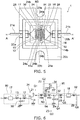
- FIG. 5 is a schematic plan view of a microwave semiconductor device according to a second embodiment.
- FIG. 6 is an equivalent circuit diagram of the microwave semiconductor device according to the second embodiment.
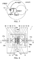
- FIG. 7 is a Smith chart describing the load impedance of the microwave semiconductor device according to the second embodiment.
- the lowest impedance point in the impedance transformation circuit occurs when the output capacitance component of the semiconductor amplifying element 24 is canceled by part of the inductance of the first bonding wire 14 of the output matching circuit 82. This is a point on the real axis in the Smith chart.
- the connection position N3 of the smoothing circuit 90 and the output matching circuit 82 is placed at the lowest impedance point in the impedance transformation circuit. This can minimize the length of the second bonding wire 23 (23a, 23b) of the smoothing circuit 90 and maximize the effect of the smoothing capacitor 34 (34a, 34b).
- a relay substrate 94 including a bonding electrode (not shown) is further provided between the semiconductor amplifying element 24 and the output matching capacitor 32.
- the relay substrate 94 is disposed along a long side 24a of the semiconductor amplifying element 24.
- the first bonding wire 14 is divided into two by the relay substrate 94. This can make a connection position N3.
- the output electrode D of the semiconductor amplifying element 24 and the bonding electrode of the relay substrate 94 are connected by a first portion 14a of the first bonding wire 14.
- the bonding electrode of the relay substrate 94 and the output matching capacitor 32 are connected by a second portion 14b of the first bonding wire 14.
- the first portion 14a of the first bonding wire 14 and the second portion 14b of the first bonding wire 14 may be continuous. For instance, use of an automatic wire bonder facilitates continuation of the first portion 14a and the second portion 14b.
- the second bonding wire 23 (23a, 23b) is connected to the bonding electrode of the relay substrate 94.
- connection position N3 is determined to lie near the point Z2@Q2 where the load impedance of the impedance transformation circuit crosses the real axis of the Smith chart (pure resistance containing only the resistance component without containing any reactance component). That is, the first portion 14a of the first bonding wire 14 and the second portion 14b of the first bonding wire 14 are provided so that the first bonding wire 14 has an inductance component resonating at the operating frequency with the output capacitance component of the semiconductor amplifying element 24. Then, the connection position N3 of the smoothing circuit 90 and the output matching circuit 82 can be placed at the lowest impedance point in the impedance transformation circuit. This can maximize the effect of the smoothing capacitor 34 (34a, 34b).
- the relay substrate 94 does not need to constitute the capacitor. Thus, the relative dielectric constant of the relay substrate is preferably lower.
- FIG. 8 is a schematic plan view of a microwave semiconductor device according to a variation of the second embodiment.
- an auxiliary substrate 95 (acting as an auxiliary smoothing capacitor) including a bonding electrode is further provided between the semiconductor amplifying element 24 and the output matching capacitor 32. Furthermore, a third bonding wire 15 is further provided to connect the output matching capacitor 32 and the bonding electrode of the auxiliary smoothing capacitor 95. Thus, the smoothing circuit is connected through the auxiliary smoothing capacitor 95. This can uniformly spread the effect of the smoothing capacitor over a plurality of parallel-connected cells. The connection position of the third bonding wire 15 is placed at the connection position N1 where the load impedance at the operating frequency is smaller than that at the connection position N2.
- the impedance at the baseband frequency of the second bonding wire 23a of the smoothing circuit can be decreased by shortening the bonding wire 23a of the smoothing circuit. This enhances the effect of the smoothing capacitor 34a at the baseband frequency.
- the smoothing circuit is uniformly connected to a plurality of parallel-connected cells. Therefore, applied voltages to the cells can be uniform and smoothed.
- the first and second embodiments and the variations associated therewith provide a microwave semiconductor device in which the application voltage to the high-frequency semiconductor amplifying element can be smoothed even if the differential frequency is as high as several hundred MHz.
- This microwave semiconductor device can be used in communication systems such as SNG (satellite news gathering) and MIMO (multiple input multiple output) based on two or more microwave signals having close frequencies.
Landscapes
- Engineering & Computer Science (AREA)
- Power Engineering (AREA)
- Microelectronics & Electronic Packaging (AREA)
- Physics & Mathematics (AREA)
- Nonlinear Science (AREA)
- Microwave Amplifiers (AREA)
- Amplifiers (AREA)
Abstract
Description
- Embodiments described herein relate generally a microwave semiconductor device.
- There is known a digital communication system having a baseband frequency of 100 MHz.
- For a baseband frequency near 100 MHz, the application voltage to the output electrode of a high-frequency semiconductor amplifying element can be smoothed by a capacitor disposed near the output terminal of the amplifier.
- On the other hand, an internally matched microwave semiconductor amplifier includes a matching circuit between the high-frequency semiconductor amplifying element and the output terminal. However, for a baseband frequency as high as 100 MHz, the applied voltage to the output electrode is difficult to smooth by a capacitor provided near the output terminal of the internally matched microwave semiconductor amplifier.
-
-
FIG. 1A is a schematic plan view of a microwave semiconductor device according to a first embodiment, andFIG. 1B is a schematic sectional view taken along line A-A'; -
FIG. 2A is an equivalent circuit diagram of the microwave semiconductor device according to the first embodiment, andFIG. 2B is a schematic plan view of the semiconductor amplifying element; -
FIG. 3 is a Smith chart describing the load impedance transformation of the microwave semiconductor device according to the first embodiment; -
FIG. 4A is a schematic plan view of a microwave semiconductor device according to a comparative example, andFIG. 4B is a Smith chart describing its load impedance transformation; -
FIG. 5 is a schematic plan view of a microwave semiconductor device according to a second embodiment; -
FIG. 6 is an equivalent circuit diagram of the microwave semiconductor device according to the second embodiment; -
FIG. 7 is a Smith chart describing the load impedance of the microwave semiconductor device according to the second embodiment; and -
FIG. 8 is a schematic plan view of a microwave semiconductor device according to a variation of the second embodiment. - In general, according to one embodiment, a microwave semiconductor device of an embodiment includes a package, a semiconductor amplifying element, an output matching circuit, and a smoothing circuit. The package includes a metal base plate, a frame body bonded to a surface of the metal base plate, an input feedthrough part bonded to the surface of the metal base plate and fitted in the frame body, and an output feedthrough part bonded to the surface of the metal base plate and fitted in the frame body at a position opposite to the input feedthrough part. The semiconductor amplifying element is bonded to a region of the surface of the metal base plate surrounded with the frame body, has an output electrode, and has a rectangular planar shape. The output matching circuit includes an output matching capacitor provided on a region of the surface of the metal base plate between the semiconductor amplifying element and the output feedthrough part and disposed along a long side direction of the semiconductor amplifying element, and a first bonding wire connected to the output matching capacitor and the output electrode. The smoothing circuit includes a smoothing capacitor provided on a region of the surface of the metal base plate adjacent to a short side of the semiconductor amplifying element, and a second bonding wire. The smoothing capacitor is connected by the second bonding wire to a position in the output matching circuit at which capacitive reactance component of a load impedance seen from the output matching capacitor is smaller than inductive reactance component of the load impedance seen from the output electrode of the semiconductor amplifying element.
- Embodiments of the invention will now be described with reference to the drawings.
-
FIG. 1A is a schematic plan view of a microwave semiconductor device according to a first embodiment.FIG. 1B is a schematic sectional view taken along line A-A'. - Here,
FIG. 1A is a schematic plan view in which thelid part 10 is removed. -
FIG. 2A is an equivalent circuit diagram of the microwave semiconductor device according to the first embodiment.FIG. 2B is a schematic plan view of the semiconductor amplifying element. - The
microwave semiconductor device 1 includes a package, asemiconductor amplifying element 24, anoutput matching circuit 82, and asmoothing circuit 90. Theoutput matching circuit 82 includes at least an output matchingcapacitor 32 and afirst bonding wire 14. - The package includes a
metal base plate 200, aframe body 16 bonded to a surface of themetal base plate 200 and made of e.g. metal, aninput feedthrough part 20a fitted in theframe body 16 and bonded to the surface of themetal base plate 200, and anoutput feedthrough part 20b fitted in theframe body 16 and bonded to the surface of themetal base plate 200 at a position opposite to theinput feedthrough part 20a. Theinput feedthrough part 20a has aninput lead 21a. Theoutput feedthrough part 20b has anoutput lead 21b. Themetal base plate 200 can be made of e.g. Cu, CuW, or CuMo. - The semiconductor amplifying
element 24 is bonded to a region of the surface of themetal base plate 200 surrounded with theframe body 16. The semiconductor amplifyingelement 24 can be e.g. HEMT (high electron mobility transistor) or MESFET (metal semiconductor field effect transistor). As shown inFIG. 2B , thesemiconductor amplifying element 24 can include an input electrode G and an output electrode D on the upper surface of the chip. Furthermore, a ground electrode S can be provided on the lower surface of the chip through a via hole provided in the chip. The semiconductor amplifyingelement 24 has a rectangular planar shape made oflong sides 24a andshort sides 24b. The semiconductor amplifyingelement 24 includes a cell region along along side 24a. The cell region is a minimum unit having an amplification function. - The output matching capacitor (C2) 32 is bonded to a region of the surface of the
metal base plate 200 between the output electrode D and theoutput feedthrough part 20b. The first bonding wire (L3) 14 connects the output electrode D with theoutput matching capacitor 32. The output matchingcapacitor 32 is disposed in parallel along along side 24a of thesemiconductor amplifying element 24. - The
microwave semiconductor device 1 can further include an input matching capacitor (C1) 30, a bonding wire (L1) 13, and a bonding wire (L2) 12. - Furthermore, the
microwave semiconductor device 1 can include an input distributedconstant circuit 17 and an output distributedconstant circuit 18. The input distributedconstant circuit 17 is configured by providing e.g. a microstrip line on aceramic substrate 26 made of e.g. Al2O3. The output distributedconstant circuit 18 is configured by providing e.g. a microstrip line on aceramic substrate 28 made of e.g. Al2O3. - In
FIG. 2A , the output matching circuit (impedance transformation circuit) 82 of themicrowave semiconductor device 1 includes thefirst bonding wire 14, theoutput matching capacitor 32, a bonding wire (L4) 19, and the output distributedconstant circuit 18. The input matching circuit (impedance transformation circuit) 80 of themicrowave semiconductor device 1 includes the input distributedconstant circuit 17, thebonding wire 13, theinput matching capacitor 30, and thebonding wire 12. Theinput matching capacitor 30 and theoutput matching capacitor 32 may have a structure in which a dielectric layer having a high relative dielectric constant of e.g. 40-280 is sandwiched between upper and lower electrodes. This can downsize each matching circuit. - The smoothing
circuit 90 includes a smoothingcapacitor 34 and a second bonding wire (LB) 23. The smoothing capacitor 34 (34a, 34b) is bonded to the surface of themetal base plate 200 so as to be adjacent to ashort side 24b of thesemiconductor amplifying element 24. The second bonding wire 23 (23a, 23b) connects the smoothingcircuit 90 with a prescribed position of theoutput matching circuit 82. - The smoothing
capacitor 34 can have a structure in which a dielectric layer having a high relative dielectric constant is sandwiched between upper and lower electrodes. Each smoothingcapacitor 34 can be provided on a region adjacent to thesemiconductor amplifying element 24. - When the
microwave semiconductor device 1 is desired to provide high output, thesemiconductor amplifying element 24 preferably has a multi-cell configuration including parallel arrangement of cell regions. - In
FIG. 2A , the smoothingcircuit 90 is connected to theoutput matching capacitor 32 at a connection position N1. The capacitance of the smoothingcapacitor 34 is denoted by CB, the value of the current amplitude by IPK, the permissible ripple voltage value by ΔV, and the value of the baseband frequency by Δf. The applied voltage at the output electrode of thesemiconductor amplifying element 24 resulting from the baseband frequency component can be smoothed by setting CB ≥ IPK × (1/2πΔf) / ΔV. - The wire length is set so that at the operating frequency, the inductance component of the second bonding wire 23 (23a, 23b) constituting the smoothing
circuit 90 has a sufficiently higher impedance than the load impedance of the matching circuit at the connection position of the smoothingcircuit 90. This reduces the operating frequency component leaking to the smoothingcapacitor 34. That is, the smoothingcircuit 90 is provided so as not to affect the operating frequency signal. - On the other hand, if the second bonding wire 23 (23a, 23b) is made too long so that the impedance is high even at the baseband frequency, then the effect of the smoothing
capacitor 34 is weakened. This hampers smoothing of the applied voltage at the output electrode of thesemiconductor amplifying element 24. -
FIG. 3 is a Smith chart describing the load impedance transformation of the microwave semiconductor device according to the first embodiment. - This figure shows the normalized impedance for a characteristic impedance (ZC) of 50 Ω. The resistance component of the
semiconductor amplifying element 24 is near e.g. 2.5 Ω, and has an output capacitance in parallel therewith. Thus, the output impedance of thesemiconductor amplifying element 24 is capacitive. Accordingly, the load impedance Z1 to be matched thereto is inductive. - The magnitude of the operating frequency component leaking to the smoothing
capacitor 34 is determined in accordance with a ration of the load impedance of the matching circuit at the connection position of the smoothingcircuit 90 to the impedance at the operating frequency of the smoothingcircuit 90. The load impedance Z2 as viewed from the second reference plane Q2 before addition of the inductive reactance due to thefirst bonding wire 14 is capacitive. - The capacitive reactance component of the load impedance Z2 is smaller than the inductive reactance component of the load impedance Z1. Thus, the load impedance Z2 of the
output matching circuit 82 at the connection position N1 of theoutput matching circuit 82 is smaller than the load impedance Z1 at the output electrode D of thesemiconductor amplifying element 24. This can maintain a large impedance ratio at the operating frequency of the smoothingcircuit 90 versus the load impedance at the operating frequency of the output matching circuit at the connection position of the smoothingcircuit 90 even if thesecond bonding wire circuit 90 is made shorter. As a result, the impedance at the baseband frequency of thesecond bonding wire circuit 90 can be lowered while sufficiently reducing the operating frequency component leaking to the smoothingcapacitor 34. This enhances the effect of the smoothingcapacitor 34 at the baseband frequency. -
FIG. 4A is a schematic plan view of a microwave semiconductor device according to a comparative example.FIG. 4B is a Smith chart describing its load impedance conversion. - This figure shows the normalized impedance for a characteristic impedance ZC of 50 Ω. In the comparative example, the
bonding wire 23a of the smoothingcircuit 190 is connected to the output electrode (not shown) of thesemiconductor amplifying element 24. That is, the inductive reactance of the load impedance Z1 as viewed from the connection position N2 is larger than the capacitive reactance of the load impedance Z2 as viewed from the second reference plane Q2 by the amount of addition of the inductive reactance due to thefirst bonding wire 14. - The load impedance Z1 at the operating frequency of the connection position N2 is higher than the load impedance Z2. By this amount, the
second bonding wire 23a of the smoothingcircuit 190 needs to be lengthened to increase the impedance of the smoothingcircuit 190 at the operating frequency. Thus, the operating frequency component leaking to the smoothingcapacitor second bonding wire 23a results in increasing the impedance at the baseband frequency of thesecond bonding wire 23a of the smoothingcircuit 190. This lowers the effect of the smoothing capacitor 134 at the baseband frequency. -
FIG. 5 is a schematic plan view of a microwave semiconductor device according to a second embodiment. -
FIG. 6 is an equivalent circuit diagram of the microwave semiconductor device according to the second embodiment. -
FIG. 7 is a Smith chart describing the load impedance of the microwave semiconductor device according to the second embodiment. - The lowest impedance point in the impedance transformation circuit occurs when the output capacitance component of the
semiconductor amplifying element 24 is canceled by part of the inductance of thefirst bonding wire 14 of theoutput matching circuit 82. This is a point on the real axis in the Smith chart. The connection position N3 of the smoothingcircuit 90 and theoutput matching circuit 82 is placed at the lowest impedance point in the impedance transformation circuit. This can minimize the length of the second bonding wire 23 (23a, 23b) of the smoothingcircuit 90 and maximize the effect of the smoothing capacitor 34 (34a, 34b). InFIG. 5 , arelay substrate 94 including a bonding electrode (not shown) is further provided between thesemiconductor amplifying element 24 and theoutput matching capacitor 32. Therelay substrate 94 is disposed along along side 24a of thesemiconductor amplifying element 24. Thefirst bonding wire 14 is divided into two by therelay substrate 94. This can make a connection position N3. - The output electrode D of the
semiconductor amplifying element 24 and the bonding electrode of therelay substrate 94 are connected by afirst portion 14a of thefirst bonding wire 14. The bonding electrode of therelay substrate 94 and theoutput matching capacitor 32 are connected by asecond portion 14b of thefirst bonding wire 14. Thefirst portion 14a of thefirst bonding wire 14 and thesecond portion 14b of thefirst bonding wire 14 may be continuous. For instance, use of an automatic wire bonder facilitates continuation of thefirst portion 14a and thesecond portion 14b. The second bonding wire 23 (23a, 23b) is connected to the bonding electrode of therelay substrate 94. - In this case, in
FIG. 7 , the connection position N3 is determined to lie near the point Z2@Q2 where the load impedance of the impedance transformation circuit crosses the real axis of the Smith chart (pure resistance containing only the resistance component without containing any reactance component). That is, thefirst portion 14a of thefirst bonding wire 14 and thesecond portion 14b of thefirst bonding wire 14 are provided so that thefirst bonding wire 14 has an inductance component resonating at the operating frequency with the output capacitance component of thesemiconductor amplifying element 24. Then, the connection position N3 of the smoothingcircuit 90 and theoutput matching circuit 82 can be placed at the lowest impedance point in the impedance transformation circuit. This can maximize the effect of the smoothing capacitor 34 (34a, 34b). Therelay substrate 94 does not need to constitute the capacitor. Thus, the relative dielectric constant of the relay substrate is preferably lower. -
FIG. 8 is a schematic plan view of a microwave semiconductor device according to a variation of the second embodiment. - In this variation, an auxiliary substrate 95 (acting as an auxiliary smoothing capacitor) including a bonding electrode is further provided between the
semiconductor amplifying element 24 and theoutput matching capacitor 32. Furthermore, athird bonding wire 15 is further provided to connect theoutput matching capacitor 32 and the bonding electrode of theauxiliary smoothing capacitor 95. Thus, the smoothing circuit is connected through theauxiliary smoothing capacitor 95. This can uniformly spread the effect of the smoothing capacitor over a plurality of parallel-connected cells. The connection position of thethird bonding wire 15 is placed at the connection position N1 where the load impedance at the operating frequency is smaller than that at the connection position N2. Thus, the impedance at the baseband frequency of thesecond bonding wire 23a of the smoothing circuit can be decreased by shortening thebonding wire 23a of the smoothing circuit. This enhances the effect of the smoothingcapacitor 34a at the baseband frequency. Furthermore, the smoothing circuit is uniformly connected to a plurality of parallel-connected cells. Therefore, applied voltages to the cells can be uniform and smoothed. - The first and second embodiments and the variations associated therewith provide a microwave semiconductor device in which the application voltage to the high-frequency semiconductor amplifying element can be smoothed even if the differential frequency is as high as several hundred MHz. This microwave semiconductor device can be used in communication systems such as SNG (satellite news gathering) and MIMO (multiple input multiple output) based on two or more microwave signals having close frequencies.
- While certain embodiments have been described, these embodiments have been presented by way of example only, and are not intended to limit the scope of the inventions as claimed. Indeed, the novel embodiments described herein may be embodied in a variety of other forms; furthermore, various omissions, substitutions and changes in the form of the embodiments described herein may be made without departing from the scope of the inventions as claimed. The accompanying claims and their equivalents are intended to cover such forms or modification as would fall within the scope of the inventions as claimed.
Claims (7)
- A microwave semiconductor device comprising:a package including a metal base plate (200), a frame body (16) bonded to a surface of the metal base plate (200), an input feedthrough part (20a) bonded to the surface of the metal base plate (200) and fitted in the frame body (16), and an output feedthrough part (20b) bonded to the surface of the metal base plate (200) and fitted in the frame body (16) at a position opposite to the input feedthrough part (20a);a semiconductor amplifying element (24) bonded to a region of the surface of the metal base plate (200) surrounded with the frame body (16), having an output electrode, and having a rectangular planar shape;an output matching circuit (82) including an output matching capacitor (32) provided on a region of the surface of the metal base plate (200) between the semiconductor amplifying element (24) and the output feedthrough part (20b) and disposed along a long side direction of the semiconductor amplifying element (24), and a first bonding wire (14) connected to the output matching capacitor (32) and the output electrode; anda smoothing circuit (90) including a smoothing capacitor (34) provided on a region of the surface of the metal base plate (200) adjacent to a short side of the semiconductor amplifying element (24), and a second bonding wire (23),the smoothing capacitor (34) being connected by the second bonding wire (23) to a position in the output matching circuit (82) at which capacitive reactance component of a load impedance seen from the output matching capacitor (32) is smaller than inductive reactance component of the load impedance seen from the output electrode of the semiconductor amplifying element (24).
- The device according to claim 1, wherein the smoothing capacitor (34) is connected to the output matching capacitor (32) by the second bonding wire (23).
- The device according to claim 1, wherein
the output matching circuit (82) further includes a relay substrate (94) provided on a region of the surface of the metal base plate (200) between the semiconductor amplifying element (24) and the output matching capacitor (32) along the long side direction of the semiconductor amplifying element (24) and having a bonding electrode on a surface thereof,
the first bonding wire (14) includes a first portion (14a) connecting the output electrode with the bonding electrode and a second portion (14b) connecting the bonding electrode with the output matching capacitor (32), and
the smoothing capacitor (34) is connected to the bonding electrode by the second bonding wire (23). - The device according to claim 3, wherein the first portion (14a) of the first bonding wire (14) has an inductance component resonating at an operating frequency with an output capacitance component of the semiconductor amplifying element (24).
- The device according to claim 3 or 4, wherein the load impedance seen from the bonding electrode is pure resistance.
- The device according to claim 1, wherein
the smoothing circuit (90) further includes an auxiliary substrate (95) provided on a region of the surface of the metal base plate (200) between the output electrode and the output matching capacitor (32) along the long side of the semiconductor amplifying element (24) and having a bonding electrode on a surface thereof, and a third bonding wire (15) connecting the output matching capacitor (32) with the bonding electrode of the auxiliary substrate (95), and
the smoothing capacitor (34) is connected to the bonding electrode of the auxiliary substrate (95) by the second bonding wire (23). - The device according to one of claims 1-6, wherein the output matching circuit (82) further includes an output distributed constant circuit (18) provided between the output matching capacitor (32) and the output feedthrough part (20b).
Applications Claiming Priority (2)
| Application Number | Priority Date | Filing Date | Title |
|---|---|---|---|
| JP2016182053 | 2016-09-16 | ||
| JP2017066958A JP6560287B2 (en) | 2016-09-16 | 2017-03-30 | Microwave semiconductor device |
Publications (2)
| Publication Number | Publication Date |
|---|---|
| EP3297159A1 true EP3297159A1 (en) | 2018-03-21 |
| EP3297159B1 EP3297159B1 (en) | 2021-03-24 |
Family
ID=58765726
Family Applications (1)
| Application Number | Title | Priority Date | Filing Date |
|---|---|---|---|
| EP17172161.6A Active EP3297159B1 (en) | 2016-09-16 | 2017-05-22 | Microwave semiconductor device |
Country Status (2)
| Country | Link |
|---|---|
| US (1) | US10110185B2 (en) |
| EP (1) | EP3297159B1 (en) |
Families Citing this family (1)
| Publication number | Priority date | Publication date | Assignee | Title |
|---|---|---|---|---|
| US20200059204A1 (en) * | 2018-08-14 | 2020-02-20 | Nxp Usa, Inc. | Amplifiers with broadband impedance matching and methods of manufacture thereof |
Citations (4)
| Publication number | Priority date | Publication date | Assignee | Title |
|---|---|---|---|---|
| US6396342B1 (en) * | 1999-10-12 | 2002-05-28 | Nec Corporation | Microwave amplifier generating distortion-reduced high output microwave power |
| EP1145314B1 (en) * | 1998-12-02 | 2007-01-03 | Infineon Technologies AG | High frequency power transistor device |
| JP5734727B2 (en) * | 2011-04-28 | 2015-06-17 | 株式会社東芝 | Semiconductor device |
| US20150349727A1 (en) * | 2014-05-28 | 2015-12-03 | Cree, Inc. | Bandwidth limiting methods for gan power transistors |
Family Cites Families (3)
| Publication number | Priority date | Publication date | Assignee | Title |
|---|---|---|---|---|
| JPS60210853A (en) * | 1984-03-06 | 1985-10-23 | Fujitsu Ltd | Semiconductor device |
| JPH06164266A (en) | 1992-11-27 | 1994-06-10 | Toshiba Corp | Microwave amplifier |
| US6633005B2 (en) * | 2001-10-22 | 2003-10-14 | Micro Mobio Corporation | Multilayer RF amplifier module |
-
2017
- 2017-05-19 US US15/600,094 patent/US10110185B2/en active Active
- 2017-05-22 EP EP17172161.6A patent/EP3297159B1/en active Active
Patent Citations (4)
| Publication number | Priority date | Publication date | Assignee | Title |
|---|---|---|---|---|
| EP1145314B1 (en) * | 1998-12-02 | 2007-01-03 | Infineon Technologies AG | High frequency power transistor device |
| US6396342B1 (en) * | 1999-10-12 | 2002-05-28 | Nec Corporation | Microwave amplifier generating distortion-reduced high output microwave power |
| JP5734727B2 (en) * | 2011-04-28 | 2015-06-17 | 株式会社東芝 | Semiconductor device |
| US20150349727A1 (en) * | 2014-05-28 | 2015-12-03 | Cree, Inc. | Bandwidth limiting methods for gan power transistors |
Also Published As
| Publication number | Publication date |
|---|---|
| EP3297159B1 (en) | 2021-03-24 |
| US10110185B2 (en) | 2018-10-23 |
| US20180083582A1 (en) | 2018-03-22 |
Similar Documents
| Publication | Publication Date | Title |
|---|---|---|
| EP3179628B1 (en) | Amplifier devices with in-package transmission line combiner | |
| JP6191016B2 (en) | Semiconductor device | |
| JP6273247B2 (en) | High frequency semiconductor amplifier | |
| US6396342B1 (en) | Microwave amplifier generating distortion-reduced high output microwave power | |
| EP3288183B1 (en) | Power transistor with harmonic control | |
| US20200059204A1 (en) | Amplifiers with broadband impedance matching and methods of manufacture thereof | |
| US12388007B2 (en) | Capacitor networks for harmonic control in power devices | |
| US5233313A (en) | High power field effect transistor amplifier | |
| US9640530B2 (en) | Semiconductor device | |
| US11855601B2 (en) | High-frequency semiconductor device | |
| US10110185B2 (en) | Microwave semiconductor device | |
| US11784610B2 (en) | Doherty amplifier module with compact wideband impedance inverter | |
| JP6560287B2 (en) | Microwave semiconductor device | |
| JP5547048B2 (en) | Power amplifier bias circuit | |
| EP3016281A1 (en) | Semiconductor amplifier bias circuit and semiconductor amplifier device | |
| CN106253873A (en) | A kind of FBAR harmonic tuning amplification module | |
| JP2021069068A (en) | Semiconductor device | |
| CN105322892A (en) | FBAR (Film Bulk Acoustic Resonator) based harmonic resonance amplifier | |
| JPH10256850A (en) | Semiconductor device and high frequency power amplifier | |
| US20150070044A1 (en) | Radio frequency characteristics measurement jig device | |
| EP0612142A2 (en) | RF transistor harmonic trap | |
| US20250183857A1 (en) | Amplifying circuit | |
| US20250175130A1 (en) | Amplifying circuit | |
| JP2023044022A (en) | Semiconductor device | |
| JP2021125713A (en) | High-frequency semiconductor device |
Legal Events
| Date | Code | Title | Description |
|---|---|---|---|
| PUAI | Public reference made under article 153(3) epc to a published international application that has entered the european phase |
Free format text: ORIGINAL CODE: 0009012 |
|
| STAA | Information on the status of an ep patent application or granted ep patent |
Free format text: STATUS: REQUEST FOR EXAMINATION WAS MADE |
|
| 17P | Request for examination filed |
Effective date: 20170522 |
|
| AK | Designated contracting states |
Kind code of ref document: A1 Designated state(s): AL AT BE BG CH CY CZ DE DK EE ES FI FR GB GR HR HU IE IS IT LI LT LU LV MC MK MT NL NO PL PT RO RS SE SI SK SM TR |
|
| AX | Request for extension of the european patent |
Extension state: BA ME |
|
| STAA | Information on the status of an ep patent application or granted ep patent |
Free format text: STATUS: EXAMINATION IS IN PROGRESS |
|
| 17Q | First examination report despatched |
Effective date: 20200221 |
|
| GRAP | Despatch of communication of intention to grant a patent |
Free format text: ORIGINAL CODE: EPIDOSNIGR1 |
|
| STAA | Information on the status of an ep patent application or granted ep patent |
Free format text: STATUS: GRANT OF PATENT IS INTENDED |
|
| INTG | Intention to grant announced |
Effective date: 20201021 |
|
| GRAS | Grant fee paid |
Free format text: ORIGINAL CODE: EPIDOSNIGR3 |
|
| GRAA | (expected) grant |
Free format text: ORIGINAL CODE: 0009210 |
|
| STAA | Information on the status of an ep patent application or granted ep patent |
Free format text: STATUS: THE PATENT HAS BEEN GRANTED |
|
| AK | Designated contracting states |
Kind code of ref document: B1 Designated state(s): AL AT BE BG CH CY CZ DE DK EE ES FI FR GB GR HR HU IE IS IT LI LT LU LV MC MK MT NL NO PL PT RO RS SE SI SK SM TR |
|
| REG | Reference to a national code |
Ref country code: GB Ref legal event code: FG4D |
|
| REG | Reference to a national code |
Ref country code: CH Ref legal event code: EP |
|
| REG | Reference to a national code |
Ref country code: DE Ref legal event code: R096 Ref document number: 602017035074 Country of ref document: DE |
|
| REG | Reference to a national code |
Ref country code: IE Ref legal event code: FG4D |
|
| REG | Reference to a national code |
Ref country code: AT Ref legal event code: REF Ref document number: 1375541 Country of ref document: AT Kind code of ref document: T Effective date: 20210415 |
|
| REG | Reference to a national code |
Ref country code: LT Ref legal event code: MG9D |
|
| PG25 | Lapsed in a contracting state [announced via postgrant information from national office to epo] |
Ref country code: HR Free format text: LAPSE BECAUSE OF FAILURE TO SUBMIT A TRANSLATION OF THE DESCRIPTION OR TO PAY THE FEE WITHIN THE PRESCRIBED TIME-LIMIT Effective date: 20210324 Ref country code: FI Free format text: LAPSE BECAUSE OF FAILURE TO SUBMIT A TRANSLATION OF THE DESCRIPTION OR TO PAY THE FEE WITHIN THE PRESCRIBED TIME-LIMIT Effective date: 20210324 Ref country code: GR Free format text: LAPSE BECAUSE OF FAILURE TO SUBMIT A TRANSLATION OF THE DESCRIPTION OR TO PAY THE FEE WITHIN THE PRESCRIBED TIME-LIMIT Effective date: 20210625 Ref country code: NO Free format text: LAPSE BECAUSE OF FAILURE TO SUBMIT A TRANSLATION OF THE DESCRIPTION OR TO PAY THE FEE WITHIN THE PRESCRIBED TIME-LIMIT Effective date: 20210624 Ref country code: BG Free format text: LAPSE BECAUSE OF FAILURE TO SUBMIT A TRANSLATION OF THE DESCRIPTION OR TO PAY THE FEE WITHIN THE PRESCRIBED TIME-LIMIT Effective date: 20210624 |
|
| PG25 | Lapsed in a contracting state [announced via postgrant information from national office to epo] |
Ref country code: RS Free format text: LAPSE BECAUSE OF FAILURE TO SUBMIT A TRANSLATION OF THE DESCRIPTION OR TO PAY THE FEE WITHIN THE PRESCRIBED TIME-LIMIT Effective date: 20210324 Ref country code: LV Free format text: LAPSE BECAUSE OF FAILURE TO SUBMIT A TRANSLATION OF THE DESCRIPTION OR TO PAY THE FEE WITHIN THE PRESCRIBED TIME-LIMIT Effective date: 20210324 Ref country code: SE Free format text: LAPSE BECAUSE OF FAILURE TO SUBMIT A TRANSLATION OF THE DESCRIPTION OR TO PAY THE FEE WITHIN THE PRESCRIBED TIME-LIMIT Effective date: 20210324 |
|
| REG | Reference to a national code |
Ref country code: NL Ref legal event code: MP Effective date: 20210324 |
|
| REG | Reference to a national code |
Ref country code: AT Ref legal event code: MK05 Ref document number: 1375541 Country of ref document: AT Kind code of ref document: T Effective date: 20210324 |
|
| PG25 | Lapsed in a contracting state [announced via postgrant information from national office to epo] |
Ref country code: NL Free format text: LAPSE BECAUSE OF FAILURE TO SUBMIT A TRANSLATION OF THE DESCRIPTION OR TO PAY THE FEE WITHIN THE PRESCRIBED TIME-LIMIT Effective date: 20210324 |
|
| PG25 | Lapsed in a contracting state [announced via postgrant information from national office to epo] |
Ref country code: SM Free format text: LAPSE BECAUSE OF FAILURE TO SUBMIT A TRANSLATION OF THE DESCRIPTION OR TO PAY THE FEE WITHIN THE PRESCRIBED TIME-LIMIT Effective date: 20210324 Ref country code: AT Free format text: LAPSE BECAUSE OF FAILURE TO SUBMIT A TRANSLATION OF THE DESCRIPTION OR TO PAY THE FEE WITHIN THE PRESCRIBED TIME-LIMIT Effective date: 20210324 Ref country code: CZ Free format text: LAPSE BECAUSE OF FAILURE TO SUBMIT A TRANSLATION OF THE DESCRIPTION OR TO PAY THE FEE WITHIN THE PRESCRIBED TIME-LIMIT Effective date: 20210324 Ref country code: EE Free format text: LAPSE BECAUSE OF FAILURE TO SUBMIT A TRANSLATION OF THE DESCRIPTION OR TO PAY THE FEE WITHIN THE PRESCRIBED TIME-LIMIT Effective date: 20210324 Ref country code: LT Free format text: LAPSE BECAUSE OF FAILURE TO SUBMIT A TRANSLATION OF THE DESCRIPTION OR TO PAY THE FEE WITHIN THE PRESCRIBED TIME-LIMIT Effective date: 20210324 |
|
| PG25 | Lapsed in a contracting state [announced via postgrant information from national office to epo] |
Ref country code: IS Free format text: LAPSE BECAUSE OF FAILURE TO SUBMIT A TRANSLATION OF THE DESCRIPTION OR TO PAY THE FEE WITHIN THE PRESCRIBED TIME-LIMIT Effective date: 20210724 Ref country code: PL Free format text: LAPSE BECAUSE OF FAILURE TO SUBMIT A TRANSLATION OF THE DESCRIPTION OR TO PAY THE FEE WITHIN THE PRESCRIBED TIME-LIMIT Effective date: 20210324 Ref country code: PT Free format text: LAPSE BECAUSE OF FAILURE TO SUBMIT A TRANSLATION OF THE DESCRIPTION OR TO PAY THE FEE WITHIN THE PRESCRIBED TIME-LIMIT Effective date: 20210726 Ref country code: RO Free format text: LAPSE BECAUSE OF FAILURE TO SUBMIT A TRANSLATION OF THE DESCRIPTION OR TO PAY THE FEE WITHIN THE PRESCRIBED TIME-LIMIT Effective date: 20210324 Ref country code: SK Free format text: LAPSE BECAUSE OF FAILURE TO SUBMIT A TRANSLATION OF THE DESCRIPTION OR TO PAY THE FEE WITHIN THE PRESCRIBED TIME-LIMIT Effective date: 20210324 |
|
| REG | Reference to a national code |
Ref country code: CH Ref legal event code: PL |
|
| REG | Reference to a national code |
Ref country code: DE Ref legal event code: R097 Ref document number: 602017035074 Country of ref document: DE |
|
| PG25 | Lapsed in a contracting state [announced via postgrant information from national office to epo] |
Ref country code: LU Free format text: LAPSE BECAUSE OF NON-PAYMENT OF DUE FEES Effective date: 20210522 Ref country code: MC Free format text: LAPSE BECAUSE OF FAILURE TO SUBMIT A TRANSLATION OF THE DESCRIPTION OR TO PAY THE FEE WITHIN THE PRESCRIBED TIME-LIMIT Effective date: 20210324 Ref country code: LI Free format text: LAPSE BECAUSE OF NON-PAYMENT OF DUE FEES Effective date: 20210531 Ref country code: DK Free format text: LAPSE BECAUSE OF FAILURE TO SUBMIT A TRANSLATION OF THE DESCRIPTION OR TO PAY THE FEE WITHIN THE PRESCRIBED TIME-LIMIT Effective date: 20210324 Ref country code: AL Free format text: LAPSE BECAUSE OF FAILURE TO SUBMIT A TRANSLATION OF THE DESCRIPTION OR TO PAY THE FEE WITHIN THE PRESCRIBED TIME-LIMIT Effective date: 20210324 Ref country code: CH Free format text: LAPSE BECAUSE OF NON-PAYMENT OF DUE FEES Effective date: 20210531 Ref country code: ES Free format text: LAPSE BECAUSE OF FAILURE TO SUBMIT A TRANSLATION OF THE DESCRIPTION OR TO PAY THE FEE WITHIN THE PRESCRIBED TIME-LIMIT Effective date: 20210324 |
|
| PLBE | No opposition filed within time limit |
Free format text: ORIGINAL CODE: 0009261 |
|
| STAA | Information on the status of an ep patent application or granted ep patent |
Free format text: STATUS: NO OPPOSITION FILED WITHIN TIME LIMIT |
|
| REG | Reference to a national code |
Ref country code: BE Ref legal event code: MM Effective date: 20210531 |
|
| GBPC | Gb: european patent ceased through non-payment of renewal fee |
Effective date: 20210624 |
|
| PG25 | Lapsed in a contracting state [announced via postgrant information from national office to epo] |
Ref country code: SI Free format text: LAPSE BECAUSE OF FAILURE TO SUBMIT A TRANSLATION OF THE DESCRIPTION OR TO PAY THE FEE WITHIN THE PRESCRIBED TIME-LIMIT Effective date: 20210324 |
|
| 26N | No opposition filed |
Effective date: 20220104 |
|
| PG25 | Lapsed in a contracting state [announced via postgrant information from national office to epo] |
Ref country code: IE Free format text: LAPSE BECAUSE OF NON-PAYMENT OF DUE FEES Effective date: 20210522 Ref country code: GB Free format text: LAPSE BECAUSE OF NON-PAYMENT OF DUE FEES Effective date: 20210624 |
|
| PG25 | Lapsed in a contracting state [announced via postgrant information from national office to epo] |
Ref country code: IS Free format text: LAPSE BECAUSE OF FAILURE TO SUBMIT A TRANSLATION OF THE DESCRIPTION OR TO PAY THE FEE WITHIN THE PRESCRIBED TIME-LIMIT Effective date: 20210724 |
|
| PG25 | Lapsed in a contracting state [announced via postgrant information from national office to epo] |
Ref country code: BE Free format text: LAPSE BECAUSE OF NON-PAYMENT OF DUE FEES Effective date: 20210531 |
|
| PG25 | Lapsed in a contracting state [announced via postgrant information from national office to epo] |
Ref country code: IT Free format text: LAPSE BECAUSE OF FAILURE TO SUBMIT A TRANSLATION OF THE DESCRIPTION OR TO PAY THE FEE WITHIN THE PRESCRIBED TIME-LIMIT Effective date: 20210324 |
|
| PG25 | Lapsed in a contracting state [announced via postgrant information from national office to epo] |
Ref country code: HU Free format text: LAPSE BECAUSE OF FAILURE TO SUBMIT A TRANSLATION OF THE DESCRIPTION OR TO PAY THE FEE WITHIN THE PRESCRIBED TIME-LIMIT; INVALID AB INITIO Effective date: 20170522 |
|
| PG25 | Lapsed in a contracting state [announced via postgrant information from national office to epo] |
Ref country code: CY Free format text: LAPSE BECAUSE OF FAILURE TO SUBMIT A TRANSLATION OF THE DESCRIPTION OR TO PAY THE FEE WITHIN THE PRESCRIBED TIME-LIMIT Effective date: 20210324 |
|
| PG25 | Lapsed in a contracting state [announced via postgrant information from national office to epo] |
Ref country code: MK Free format text: LAPSE BECAUSE OF FAILURE TO SUBMIT A TRANSLATION OF THE DESCRIPTION OR TO PAY THE FEE WITHIN THE PRESCRIBED TIME-LIMIT Effective date: 20210324 |
|
| PG25 | Lapsed in a contracting state [announced via postgrant information from national office to epo] |
Ref country code: TR Free format text: LAPSE BECAUSE OF FAILURE TO SUBMIT A TRANSLATION OF THE DESCRIPTION OR TO PAY THE FEE WITHIN THE PRESCRIBED TIME-LIMIT Effective date: 20210324 |
|
| PG25 | Lapsed in a contracting state [announced via postgrant information from national office to epo] |
Ref country code: MT Free format text: LAPSE BECAUSE OF FAILURE TO SUBMIT A TRANSLATION OF THE DESCRIPTION OR TO PAY THE FEE WITHIN THE PRESCRIBED TIME-LIMIT Effective date: 20210324 |
|
| PGFP | Annual fee paid to national office [announced via postgrant information from national office to epo] |
Ref country code: DE Payment date: 20250325 Year of fee payment: 9 |
|
| PGFP | Annual fee paid to national office [announced via postgrant information from national office to epo] |
Ref country code: FR Payment date: 20250401 Year of fee payment: 9 |