EP3297031A1 - Thin-film transistor, array substrate and preparation methods therefor, and display device - Google Patents
Thin-film transistor, array substrate and preparation methods therefor, and display device Download PDFInfo
- Publication number
- EP3297031A1 EP3297031A1 EP15885767.2A EP15885767A EP3297031A1 EP 3297031 A1 EP3297031 A1 EP 3297031A1 EP 15885767 A EP15885767 A EP 15885767A EP 3297031 A1 EP3297031 A1 EP 3297031A1
- Authority
- EP
- European Patent Office
- Prior art keywords
- layer
- lanthanum boride
- pattern
- tft
- semiconductor active
- Prior art date
- Legal status (The legal status is an assumption and is not a legal conclusion. Google has not performed a legal analysis and makes no representation as to the accuracy of the status listed.)
- Granted
Links
Images



Classifications
-
- H—ELECTRICITY
- H10—SEMICONDUCTOR DEVICES; ELECTRIC SOLID-STATE DEVICES NOT OTHERWISE PROVIDED FOR
- H10D—INORGANIC ELECTRIC SEMICONDUCTOR DEVICES
- H10D62/00—Semiconductor bodies, or regions thereof, of devices having potential barriers
- H10D62/80—Semiconductor bodies, or regions thereof, of devices having potential barriers characterised by the materials
-
- H—ELECTRICITY
- H10—SEMICONDUCTOR DEVICES; ELECTRIC SOLID-STATE DEVICES NOT OTHERWISE PROVIDED FOR
- H10D—INORGANIC ELECTRIC SEMICONDUCTOR DEVICES
- H10D30/00—Field-effect transistors [FET]
- H10D30/01—Manufacture or treatment
- H10D30/021—Manufacture or treatment of FETs having insulated gates [IGFET]
- H10D30/031—Manufacture or treatment of FETs having insulated gates [IGFET] of thin-film transistors [TFT]
-
- H—ELECTRICITY
- H10—SEMICONDUCTOR DEVICES; ELECTRIC SOLID-STATE DEVICES NOT OTHERWISE PROVIDED FOR
- H10D—INORGANIC ELECTRIC SEMICONDUCTOR DEVICES
- H10D30/00—Field-effect transistors [FET]
- H10D30/60—Insulated-gate field-effect transistors [IGFET]
- H10D30/67—Thin-film transistors [TFT]
- H10D30/674—Thin-film transistors [TFT] characterised by the active materials
- H10D30/675—Group III-V materials, Group II-VI materials, Group IV-VI materials, selenium or tellurium
-
- H—ELECTRICITY
- H10—SEMICONDUCTOR DEVICES; ELECTRIC SOLID-STATE DEVICES NOT OTHERWISE PROVIDED FOR
- H10D—INORGANIC ELECTRIC SEMICONDUCTOR DEVICES
- H10D30/00—Field-effect transistors [FET]
- H10D30/60—Insulated-gate field-effect transistors [IGFET]
- H10D30/67—Thin-film transistors [TFT]
- H10D30/674—Thin-film transistors [TFT] characterised by the active materials
- H10D30/6755—Oxide semiconductors, e.g. zinc oxide, copper aluminium oxide or cadmium stannate
-
- H—ELECTRICITY
- H10—SEMICONDUCTOR DEVICES; ELECTRIC SOLID-STATE DEVICES NOT OTHERWISE PROVIDED FOR
- H10D—INORGANIC ELECTRIC SEMICONDUCTOR DEVICES
- H10D30/00—Field-effect transistors [FET]
- H10D30/60—Insulated-gate field-effect transistors [IGFET]
- H10D30/67—Thin-film transistors [TFT]
- H10D30/6757—Thin-film transistors [TFT] characterised by the structure of the channel, e.g. transverse or longitudinal shape or doping profile
-
- H—ELECTRICITY
- H10—SEMICONDUCTOR DEVICES; ELECTRIC SOLID-STATE DEVICES NOT OTHERWISE PROVIDED FOR
- H10D—INORGANIC ELECTRIC SEMICONDUCTOR DEVICES
- H10D30/00—Field-effect transistors [FET]
- H10D30/60—Insulated-gate field-effect transistors [IGFET]
- H10D30/67—Thin-film transistors [TFT]
- H10D30/6758—Thin-film transistors [TFT] characterised by the insulating substrates
-
- H—ELECTRICITY
- H10—SEMICONDUCTOR DEVICES; ELECTRIC SOLID-STATE DEVICES NOT OTHERWISE PROVIDED FOR
- H10D—INORGANIC ELECTRIC SEMICONDUCTOR DEVICES
- H10D48/00—Individual devices not covered by groups H10D1/00 - H10D44/00
- H10D48/30—Devices controlled by electric currents or voltages
-
- H—ELECTRICITY
- H10—SEMICONDUCTOR DEVICES; ELECTRIC SOLID-STATE DEVICES NOT OTHERWISE PROVIDED FOR
- H10D—INORGANIC ELECTRIC SEMICONDUCTOR DEVICES
- H10D86/00—Integrated devices formed in or on insulating or conducting substrates, e.g. formed in silicon-on-insulator [SOI] substrates or on stainless steel or glass substrates
- H10D86/01—Manufacture or treatment
- H10D86/021—Manufacture or treatment of multiple TFTs
- H10D86/0221—Manufacture or treatment of multiple TFTs comprising manufacture, treatment or patterning of TFT semiconductor bodies
-
- H—ELECTRICITY
- H10—SEMICONDUCTOR DEVICES; ELECTRIC SOLID-STATE DEVICES NOT OTHERWISE PROVIDED FOR
- H10D—INORGANIC ELECTRIC SEMICONDUCTOR DEVICES
- H10D86/00—Integrated devices formed in or on insulating or conducting substrates, e.g. formed in silicon-on-insulator [SOI] substrates or on stainless steel or glass substrates
- H10D86/01—Manufacture or treatment
- H10D86/021—Manufacture or treatment of multiple TFTs
- H10D86/0231—Manufacture or treatment of multiple TFTs using masks, e.g. half-tone masks
-
- H—ELECTRICITY
- H10—SEMICONDUCTOR DEVICES; ELECTRIC SOLID-STATE DEVICES NOT OTHERWISE PROVIDED FOR
- H10D—INORGANIC ELECTRIC SEMICONDUCTOR DEVICES
- H10D86/00—Integrated devices formed in or on insulating or conducting substrates, e.g. formed in silicon-on-insulator [SOI] substrates or on stainless steel or glass substrates
- H10D86/40—Integrated devices formed in or on insulating or conducting substrates, e.g. formed in silicon-on-insulator [SOI] substrates or on stainless steel or glass substrates characterised by multiple TFTs
- H10D86/421—Integrated devices formed in or on insulating or conducting substrates, e.g. formed in silicon-on-insulator [SOI] substrates or on stainless steel or glass substrates characterised by multiple TFTs having a particular composition, shape or crystalline structure of the active layer
- H10D86/423—Integrated devices formed in or on insulating or conducting substrates, e.g. formed in silicon-on-insulator [SOI] substrates or on stainless steel or glass substrates characterised by multiple TFTs having a particular composition, shape or crystalline structure of the active layer comprising semiconductor materials not belonging to the Group IV, e.g. InGaZnO
-
- H—ELECTRICITY
- H10—SEMICONDUCTOR DEVICES; ELECTRIC SOLID-STATE DEVICES NOT OTHERWISE PROVIDED FOR
- H10D—INORGANIC ELECTRIC SEMICONDUCTOR DEVICES
- H10D86/00—Integrated devices formed in or on insulating or conducting substrates, e.g. formed in silicon-on-insulator [SOI] substrates or on stainless steel or glass substrates
- H10D86/40—Integrated devices formed in or on insulating or conducting substrates, e.g. formed in silicon-on-insulator [SOI] substrates or on stainless steel or glass substrates characterised by multiple TFTs
- H10D86/60—Integrated devices formed in or on insulating or conducting substrates, e.g. formed in silicon-on-insulator [SOI] substrates or on stainless steel or glass substrates characterised by multiple TFTs wherein the TFTs are in active matrices
-
- H—ELECTRICITY
- H10—SEMICONDUCTOR DEVICES; ELECTRIC SOLID-STATE DEVICES NOT OTHERWISE PROVIDED FOR
- H10D—INORGANIC ELECTRIC SEMICONDUCTOR DEVICES
- H10D99/00—Subject matter not provided for in other groups of this subclass
-
- H—ELECTRICITY
- H10—SEMICONDUCTOR DEVICES; ELECTRIC SOLID-STATE DEVICES NOT OTHERWISE PROVIDED FOR
- H10P—GENERIC PROCESSES OR APPARATUS FOR THE MANUFACTURE OR TREATMENT OF DEVICES COVERED BY CLASS H10
- H10P14/00—Formation of materials, e.g. in the shape of layers or pillars
- H10P14/20—Formation of materials, e.g. in the shape of layers or pillars of semiconductor materials
- H10P14/22—Formation of materials, e.g. in the shape of layers or pillars of semiconductor materials using physical deposition, e.g. vacuum deposition or sputtering
-
- H—ELECTRICITY
- H10—SEMICONDUCTOR DEVICES; ELECTRIC SOLID-STATE DEVICES NOT OTHERWISE PROVIDED FOR
- H10P—GENERIC PROCESSES OR APPARATUS FOR THE MANUFACTURE OR TREATMENT OF DEVICES COVERED BY CLASS H10
- H10P14/00—Formation of materials, e.g. in the shape of layers or pillars
- H10P14/20—Formation of materials, e.g. in the shape of layers or pillars of semiconductor materials
- H10P14/34—Deposited materials, e.g. layers
- H10P14/3402—Deposited materials, e.g. layers characterised by the chemical composition
- H10P14/3434—Deposited materials, e.g. layers characterised by the chemical composition being oxide semiconductor materials
Definitions
- the present disclosure relates to the field of display technology, in particular to a thin film transistor (TFT), an array substrate, their manufacturing methods, and a display device.
- TFT thin film transistor
- TFT is used to control and drive a subpixel of a liquid crystal display (LCD) and an organic light-emitting diode (OLED) display.
- LCD liquid crystal display
- OLED organic light-emitting diode
- amorphous silicon (a-Si) TFTs have been gradually replaced with lower temperature poly-silicon (LTPS) TFTs, metal-induced lateral crystallization (MILC) TFTs and oxide TFTs.
- LTPS lower temperature poly-silicon
- MILC metal-induced lateral crystallization
- oxide TFT For the commonly-used oxide TFT, an oxide semiconductor is used as an active layer, so it has such advantages as large mobility rate, high on-state current, excellent switching characteristic and excellent uniformity.
- the oxide TFT may be applied to a display device where rapid response and large current are required, e.g., a high-frequency, high-resolution and large-scale display device or an organic light-emitting display device.
- the oxide semiconductors contain some rare metal elements, e.g., indium and strontium.
- An abundance of indium in the earth's crust is merely about 0.049ppm. Due to the excessive consumption of indium, elemental indium becomes less and less, so its price becomes higher and higher. As a result, the production cost of the display device will increase, and the mass production thereof will be limited.
- An object of the present disclosure is to provide a TFT, an array substrate, their manufacturing methods, and a display device, so as to reduce a usage amount of indium in a semiconductor active layer, thereby to reduce the production cost.
- the present disclosure provides in some embodiments a method for manufacturing a TFT, including a step of forming a pattern of a semiconductor active layer on a transparent substrate through a patterning process, the pattern of the semiconductor active layer including a lanthanum boride pattern.
- the present disclosure provides in some embodiments a method for manufacturing an array substrate, including the above-mentioned method for manufacturing a TFT.
- the present disclosure provides in some embodiments a TFT including a pattern of a semiconductor active layer.
- the pattern of the semiconductor active layer includes a lanthanum boride pattern.
- the present disclosure provides in some embodiments an array substrate including the above-mentioned TFT.
- the present disclosure provides in some embodiments a display device including the above-mentioned array substrate.
- the method for manufacturing the TFT includes a step of forming the pattern of the semiconductor active layer on the transparent substrate through a patterning process, and the pattern of the semiconductor active layer includes the lanthanum boride pattern.
- the semiconductor active layer may include lanthanum boride as a main component.
- lanthanum is a rare earth element, its abundance in the earth's crust is 30 ppm, far greater than the abundance of indium. In addition, annual consumption of lanthanum is also far less than that of indium.
- the semiconductor active layer made of lanthanum boride is obviously advantageous over the semiconductor active layer containing indium in terms of the production cost and the sustainable usage.
- lanthanum is located at a body center of a cube.
- Six boron elements form a regular octahedron, and a body center of each regular octahedron is located at a vertex of the cube.
- Electron orbits of the lanthanum elements in adjacent lattices may overlap each other to form an electronic channel.
- lanthanum boride has very high mobility and conductivity
- the semiconductor active layer made of lanthanum boride has high electron mobility.
- any technical or scientific term used herein shall have the common meaning understood by a person of ordinary skills.
- Such words as “first” and “second” used in the specification and claims are merely used to differentiate different components rather than to represent any order, number or importance.
- such words as “one” or “one of” are merely used to represent the existence of at least one member, rather than to limit the number thereof.
- Such words as “connect” or “connected to” may include electrical connection, direct or indirect, rather than to be limited to physical or mechanical connection.
- Such words as “on”, “under”, “left” and “right” are merely used to represent relative position relationship, and when an absolute position of the object is changed, the relative position relationship will be changed too.
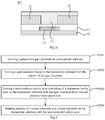
- the present disclosure provides in some embodiments a method for manufacturing a TFT which, as shown in Fig.1 , may include: Step S101 of, as shown in Fig.2a , forming a pattern of a gate electrode 11 on a transparent substrate 10 through a patterning process; Step S102 of forming a gate insulation layer 12 on the transparent substrate 10 through a patterning process; Step S103 of forming a pattern of a semiconductor active layer 13 on the transparent substrate 10, the pattern of the semiconductor active layer 13 including a lanthanum boride pattern; and Step S104 of forming patterns of a source electrode 14 and a drain electrode 15 on the transparent substrate 10 through a patterning process.
- Step S101 may be performed at first, so as to form the pattern of the gate electrode 11 on the transparent substrate 10; next, the gate insulation layer 12 may be formed on the transparent substrate with the pattern of the gate electrode 11; then, the pattern of the semiconductor active layer 13 including the lanthanum pattern may be formed on the transparent substrate with the gate insulation layer 12; and finally, the patterns of the source electrode 14 and the drain electrode 15 may be formed on the transparent substrate with the pattern of the semiconductor active layer 13.
- Step S103 may be performed at first, so as to form the pattern of the semiconductor active layer 13 including the lanthanum boride pattern on the transparent substrate 10; next, the patterns of the source electrode 14 and the drain electrode 15 may be formed on the transparent substrate with the pattern of the semiconductor active layer 13; and then, the gate insulation layer 12 and the pattern of the gate electrode 11 may be formed sequentially on the transparent substrate with the patterns of the source electrode 14 and the drain electrode 15.
- the bottom-gate TFT and the top-gate TFT depend on positions of the gate electrode 11 and the gate insulation layer 12.
- the TFT is a bottom-gate TFT.
- the TFT is a top-gate TFT.
- the bottom-gate TFT as an example. Of course, it may also be applied to the top-gate TFT, which also falls within the scope of the present disclosure. Due to an identical principle, the top-gate TFT will not be particularly defined hereinafter.
- Steps S101, S102 and S104 may refer to those in the related art.
- the patterning processes mentioned in the embodiments of the present disclosure may include an photoetching process, or including the photoetching process and an etching process.
- the patterning process may further include any other processes for forming a predetermined pattern, e.g., a printing process or an ink-jetting process.
- the photoetching process includes such processes as film-forming, exposing and developing, and specifically, it may include any processes for forming a pattern using a photoresist, a mask plate and an exposure machine.
- the corresponding patterning process may be selected in accordance with the structure to be formed.
- the transparent substrate 10 may be made of a hard material, e.g., a glass substrate, a hard resin substrate, or a transparent substrate made of a flexible material.
- the layers may be directly formed on a surface of the transparent substrate 10, or formed on the transparent substrate 10 on which some other layers or patterns have already been formed.
- the semiconductor active layer 13 is mainly made of La x B y .
- x may be a value within a range of 0.05 to 1.
- the values of y and x may be adjusted in accordance with the practical need. The larger the content of boron, the lower the concentration of carriers and the conductivity. At this time, it is able to convert lanthanum boride from a conductor into a semiconductor.
- the single layer may be a lanthanum boride layer.
- the lanthanum boride layer may be an intermediate layer of the plurality of layers, and the lanthanum boride layer may be of a thickness larger than the other layers.
- the other layers may be made of a metal oxide semiconductor, e.g., indium gallium zinc oxide (IGZO). Because the content of indium in the entire semiconductor active layer 13 is smaller than lanthanum boride, so it is able to reduce the usage content of indium, thereby to reduce the production cost.
- IGZO indium gallium zinc oxide
- lanthanum boride also has such advantages as high melting point, resistance to ion bombardment, anti-oxidation, heat conduction and excellent chemical stability. Further, it has mobility higher than a-Si.
- the method for manufacturing the TFT includes the step of forming the pattern of the semiconductor active layer on the transparent substrate through a patterning process, and the pattern of the semiconductor active layer includes the lanthanum boride pattern.
- the semiconductor active layer may include lanthanum boride as a main component.
- lanthanum is a rare earth element, its abundance in the earth's crust is 30 ppm, far greater than the abundance of indium.
- annual consumption of lanthanum is also far less than that of indium.
- the semiconductor active layer made of lanthanum boride is obviously advantageous over the semiconductor active layer containing indium in terms of the production cost and the sustainable usage.
- lanthanum is located at a body center of a cube.
- Six boron elements form a regular octahedron, and a body center of each regular octahedron is located at a vertex of the cube.
- Electron orbits of the lanthanum elements in adjacent lattices may overlap each other to form an electronic channel.
- lanthanum boride has very high mobility and conductivity, and the semiconductor active layer made of lanthanum boride has high electron mobility.
- it is able to increase an on/off current ratio of the resultant TFT, thereby to prevent the occurrence of current leakage conveniently.
- it is able to increase a charging rate of the display device, thereby to improve a display effect.
- the method in this embodiment is used to manufacture the TFT in Fig.2a , where the semiconductor active layer 13 mainly containing lanthanum boride is formed through physical vapor deposition. As shown in Fig.3 , the method may include the following steps.
- Step S201 forming the pattern of the gate electrode 11 on the transparent substrate 10.
- a gate metal layer having a thickness of 100nm to 2000nm on the transparent substrate 10 through physical vapor deposition.
- the gate metal layer may be made of a metal, a metal alloy or a conductive metal oxide. It may consist of two or more layers made of a conductive material, e.g., two molybdenum (Mo) layers and an aluminum (Al) layer arranged between the two Mo layers, i.e., Mo/Al/Mo.
- a photoresist may be applied onto a surface of the gate metal layer, and the gate metal layer may be exposed, developed and etched using a common mask plate, so as to expose a part of the surface of the gate metal layer. Then, a portion of the gate metal layer not covered by the photoresist may be etched, so as to form the pattern of the gate electrode 11.
- Step S202 forming the gate insulation layer 12 on the transparent substrate with the pattern of the gate electrode 11.
- the gate insulation layer 12 may be formed on the transparent substrate with the pattern of the gate electrode 11 through physical vapor deposition, chemical vapor deposition, electrochemical oxidation or thermal oxidation, and the gate insulation layer 12 may have a thickness of 50nm to 1000nm.
- the gate insulation layer may be made of at least one of SiO 2 , SiN x , SiON, Al 2 O 3 , Ta 2 O 5 , Y 2 O 3 or HfO 2 .
- Step S203 forming the semiconductor lanthanum boride layer on the transparent substrate with the gate insulation layer 12 through physical vapor deposition.
- the lanthanum boride layer may be formed at an atmospheric pressure of 0.02Pa to 0.5Pa. In the case that the atmospheric pressure is less than 0.02Pa or greater than 0.5Pa, the performance of lanthanum boride may be degraded. In order to improve the stability of the lanthanum boride layer, optionally, the atmospheric pressure may be 0.05Pa to 0.3Pa.
- the lanthanum boride layer may grow at a rate of 10nm/min to 100nm/min. In the case that the growth rate of the lanthanum boride layer is less than 10nm/min, the production efficiency may decrease, and in the case that the growth rate is greater than 100nm/min, the performance of the lanthanum boride layer may be degraded. It should be appreciated that, for the lanthanum boride layer, the concentration of carriers and the conductivity of the lanthanum boride layer may decreases along with an increase in the content of boron, so as to convert lanthanum boride from a conductor to a semiconductor conveniently.
- the growth rate may be 20nm/min to 100nm/min.
- the atmospheric pressure may be an atmospheric pressure in a physical vapor deposition chamber, and during the formation thereof through sputtering, the atmospheric pressure may be a sputtering pressure for a target.
- the resultant lanthanum boride layer may have a thickness of 10nm to 500nm.
- the performance of the TFT may be affected by the layers of the TFT, especially the semiconductor active layer. In the case that the thickness of the lanthanum boride layer is less than 10nm or greater than 500nm, the stability, and thereby the yield, of the TFT may decrease. In order to improve the stability of the TFT, the thickness of the lanthanum boride layer may be 20nm to 200nm.
- the lanthanum boride layer may have a thickness greater than the other layers, e.g., it may have a thickness of 10nm to 500nm.
- the other layers may each be of a thickness of 10nm to 50nm, and made of a metal oxide semiconductor, e.g., IGZO. Because the content of indium in the entire semiconductor active layer 13 is smaller than lanthanum boride, so it is able to reduce the usage content of indium, thereby to reduce the production cost.
- the concentration of the carriers in the lanthanum boride layer may be controlled within a range of 10 15 cm -3 to 10 18 cm -3 , so as to convert the lanthanum boride layer into a semiconductor.
- the concentration of the carriers is less than 10 15 cm -3
- the electron mobility of the lanthanum boride layer may be too low
- the concentration of the carriers is greater than 10 18 cm -3
- the current leakage of the TFT may increase, and thereby the switching characteristic of the TFT may be adversely affected.
- the concentration of the carriers increases continuously, the semiconductor active layer may become a conductor, and the TFT may become invalid.
- lanthanum is less affected by pressure than boron, so the pressure of an inertia gas such as argon or nitrogen may be reduced appropriately in the case that the lanthanum boride layer is formed by physical vapor deposition. In this way, it is able to facilitate the position of boron onto the substrate and increase the content of boron in the lanthanum boride layer, thereby to reduce the concentration of the carriers and the conductivity, and facilitate the conversion of the lanthanum boride layer from a conductor into a semiconductor.
- an inertia gas such as argon or nitrogen
- a photoresist may be applied onto a surface of the lanthanum boride layer. Then, the photoresist may be subjected to a masking process, an exposing process and a developing process using a common mask plate, so as to expose a part of the surface of the lanthanum boride layer. Next, the lanthanum boride layer not covered by the photoresist may be etched, so as to form the pattern of the semiconductor active layer 13.
- Step S204 forming patterns of the source electrode 14 and the drain electrode 15 on the transparent substrate with the semiconductor active layer 13.
- a data metal layer having a thickness of 100nm to 1000nm may be formed on the transparent substrate with the semiconductor active layer 13 through physical vapor deposition.
- the data metal layer may be made of a metal, a metal alloy or a conductive metal oxide. It may consist of more than two layers, e.g., two Mo layers and an Al metal layer arranged between the two Mo layers, i.e., Mo/Al/Mo.
- a photoresist may be applied to a surface of the data metal layer, and then subjected to a masking process, an exposing process and a developing process, so as to expose a part of the surface of the data metal layer. Then, the data metal layer not covered by the photoresist may be etched, so as to form the patterns of the source electrode 14 and the drain electrode 15.
- the semiconductor active layer 13 mainly containing lanthanum boride is manufactured through physical vapor deposition.
- the method for manufacturing the TFT will be described in the following embodiments by taking the semiconductor active layer 13 formed through sputtering as an example.
- the method in this embodiment may be used to manufacture the TFT as shown in Fig.2a , and it may include the following steps.
- an Al layer having a thickness of 300nm may be formed on the transparent substrate 10, and then subjected to masking, exposing, etching and developing processes to form the pattern of the gate electrode 11.
- the gate insulation layer 12 having a thickness of 200nm may be formed on the transparent substrate with the pattern of the gate electrode 11 through anodic oxidation.
- the lanthanum boride layer may be formed on the transparent substrate with the gate insulation layer 12 through sputtering.
- a lanthanum boride target may be placed on a sputtering device, so as to form the lanthanum boride layer having a thickness of 20nm through sputtering at an atmospheric pressure of 0.3Pa and a growth rate of 10nm/min.
- the lanthanum boride layer may be subjected to masking, exposing, developing and etching processes, so as to form the pattern of the semiconductor active layer 13.
- the semiconductor active layer 13 has a concentration of carriers of about 10 18 cm -3 , and a mobility rate of about 3cm 2 /Vs.
- an ITO layer having a thickness of 380nm may be formed on the transparent substrate with the semiconductor active layer 13 through sputtering, and then subjected to masking, exposing, developing and etching processes so as to form the patterns of the source electrode 14 and the drain electrode 15.
- Fig.4 shows a transfer characteristic curve of the resultant TFT.
- a drain current is about 10 -95 A.
- the method in this embodiment may be used to manufacture the TFT as shown in Fig.2c .
- the semiconductor active layer 13 is arranged above the source electrode 14 and the drain electrode 15, so the step of forming the semiconductor active layer 13 is performed subsequent to the step of forming the source electrode 14 and the drain electrode 15.
- the steps of forming the other layers in the method may be identical to those mentioned in the second embodiment.
- the step of forming the semiconductor active layer 13 includes forming the lanthanum boride layer on the transparent substrate with the source electrode 14 and the drain electrode 15 through sputtering, and then forming the pattern of the semiconductor active layer 13 through masking, exposing, etching and developing processes.
- a lanthanum boride target may be placed on a sputtering device, so as to form the lanthanum boride layer having a thickness of 40nm through sputtering at an atmospheric pressure of 0.1Pa and a growth rate of 20nm/min.
- the resultant semiconductor active layer 13 may have a concentration of carriers of about 10 17 cm -3 and a mobility rate of about 1.5cm 2 /Vs.
- Fig.5 shows a transfer characteristic curve of the resultant TFT.
- a drain current is about 10 -9 A.
- the method in this embodiment may be used to manufacture the TFT as shown in Fig.2a . Except the step of forming the semiconductor active layer 13, the steps of forming the other layers in the method may be identical to those mentioned in the second embodiment.
- the step of forming the semiconductor active layer 13 includes forming the lanthanum boride layer on the transparent substrate with the gate insulation layer 12 through sputtering, and then forming the pattern of the semiconductor active layer 13 through masking, exposing, etching and developing processes.
- a lanthanum boride target may be placed on a sputtering device, so as to form the lanthanum boride layer having a thickness of 100nm through sputtering at an atmospheric pressure of 0.05Pa and a growth rate of 30nm/min.
- the resultant semiconductor active layer 13 may have a concentration of carriers of about 10 15 cm -3 and a mobility rate of about 2.8cm 2 /Vs.
- Fig.6 shows a transfer characteristic curve of the resultant TFT.
- a drain current is about 10 -10.5 A.
- the TFT in the fourth embodiment has a minimal drain current, i.e., the minimal off-state current.
- the curve in Fig.6 has a maximal slope, so the drain current of the TFT in the fourth embodiment may increase most rapidly.
- the TFT in the fourth embodiment have the most rapid switch response speed and the best switching characteristic.
- the present disclosure further provides in some embodiments a method for manufacturing an array substrate, including the above-mentioned method for manufacturing the TFT.
- a method for manufacturing an array substrate including the above-mentioned method for manufacturing the TFT.
- the steps of the method for manufacturing the TFT and the beneficial effects thereof have been described hereinbefore, and thus will not be particularly defined herein.
- the method for manufacturing the array substrate may include the following steps.
- a gate metal layer having a thickness of 100nm to 2000nm may be formed on the transparent substrate 10 through physical vapor deposition.
- a photoresist may be applied onto a surface of the gate metal layer, and then subjected to exposing, developing and etching processes with a common mask plate, so as to expose a part of the surface of the gate metal layer.
- the gate metal layer not covered by the photoresist may be etched, so as to form patterns of the gate electrode 11 and a gate line.
- the gate insulation layer 12 having a thickness of 50nm to 1000nm may be formed on the transparent substrate with the patterns of the gate electrode and the gate line through physical vapor deposition, chemical vapor deposition, electrochemical oxidation or thermal oxidation.
- the semiconductor lanthanum boride layer may be formed on the transparent substrate with the gate insulation layer 12 through physical vapor deposition.
- the formation of the lanthanum boride layer may refer to that mentioned in the first embodiment.
- a photoresist may be applied onto a surface of the lanthanum boride layer, and then subjected to exposing, developing and etching processes with a common mask plate, so as to expose a part of the surface of the lanthanum boride layer. Then, the lanthanum boride layer not covered by the photoresist may be etched, so as to form the pattern of the semiconductor active layer 13.
- the data metal layer having a thickness of 100nm to 1000nm may be formed on the transparent substrate with the semiconductor active layer 13.
- a photoresist may be applied onto a surface of the data metal layer, and then subjected to exposing, developing and etching processes with a common mask plate, so as to expose a part of the surface of the data metal layer. Then, the data metal layer not covered by the photoresist may be etched, so as to form patterns of the source electrode 14, the drain electrode 15 and a data line.
- the passivation layer may be formed on the transparent substrate with the patterns of the source electrode 14, the drain electrode 15 and the data line.
- the via-hole may be formed in the passivation layer through a patterning process, so as to expose a portion of the drain electrode 15.
- a pixel electrode may be formed on the passivation layer with the via-hole through a patterning process, so that the pixel electrode is connected to the drain electrode 15 through the via-hole.
- the array substrate including the TFT as shown in Fig.2a as an example.
- the array substrate including the TFT as shown in Fig.2b or 2c or including both the pixel electrode and a common electrode, will also fall within the scope of the present disclosure.
- the present disclosure further provides in some embodiments a TFT which, as shown in Fig.2a, 2b or 2c , may include the gate electrode 11, the gate insulation layer 12, the semiconductor active layer 13, the source electrode 14 and the drain electrode 15.
- the semiconductor active layer 13 may mainly consist of lanthanum boride.
- the lanthanum boride layer may have a thickness of 10nm to 500nm.
- the performance of the TFT may be affected by the layers of the TFT, especially the semiconductor active layer. In the case that the thickness of the lanthanum boride layer is less than 10nm or greater than 500nm, the stability, and thereby the yield, of the TFT may decrease.
- the semiconductor active layer may include lanthanum boride as a main component.
- lanthanum is a rare earth element, its abundance in the earth's crust is 30 ppm, far greater than the abundance of indium.
- annual consumption of lanthanum is also far less than that of indium.
- the semiconductor active layer made of lanthanum boride is obviously advantageous over the semiconductor active layer containing indium in terms of the production cost and the sustainable usage.
- lanthanum is located at a body center of a cube. Six boron elements form a regular octahedron, and a body center of each regular octahedron is located at a vertex of the cube.
- Electron orbits of the lanthanum elements in adjacent lattices may overlap each other to form an electronic channel.
- lanthanum boride has very high mobility and conductivity, and the semiconductor active layer made of lanthanum boride has high electron mobility.
- it is able to increase an on/off current ratio of the resultant TFT, thereby to control the current leakage conveniently.
- it is able to increase a charging rate of the display device, thereby to improve a display effect.
- the present disclosure further provides in some embodiments an array substrate including the above-mentioned TFT.
- the structure of the TFT and the beneficial effects thereof have been described hereinbefore, and thus will not be particularly defined herein.
- the present disclosure further provides in some embodiments a display device including the above-mentioned array substrate.
- the display device may be a liquid crystal display device.
- it may be any product or member having a display function, such as liquid crystal display, liquid crystal television, digital photo frame, mobile phone or flat-panel computer.
- the structure of the array substrate and the beneficial effects thereof have been described hereinbefore, and thus will not be particularly defined herein.
Landscapes
- Thin Film Transistor (AREA)
Abstract
Description
- The present application claims a priority of the Chinese Patent Application No.
201510236824.3 filed on May 11, 2015 - The present disclosure relates to the field of display technology, in particular to a thin film transistor (TFT), an array substrate, their manufacturing methods, and a display device.
- As the most important electronic element in the field of display technology, TFT is used to control and drive a subpixel of a liquid crystal display (LCD) and an organic light-emitting diode (OLED) display.
- Along with the rapid development of the display technology, amorphous silicon (a-Si) TFTs have been gradually replaced with lower temperature poly-silicon (LTPS) TFTs, metal-induced lateral crystallization (MILC) TFTs and oxide TFTs.
- For the commonly-used oxide TFT, an oxide semiconductor is used as an active layer, so it has such advantages as large mobility rate, high on-state current, excellent switching characteristic and excellent uniformity. The oxide TFT may be applied to a display device where rapid response and large current are required, e.g., a high-frequency, high-resolution and large-scale display device or an organic light-emitting display device.
- However, in the related art, most of the oxide semiconductors contain some rare metal elements, e.g., indium and strontium. An abundance of indium in the earth's crust is merely about 0.049ppm. Due to the excessive consumption of indium, elemental indium becomes less and less, so its price becomes higher and higher. As a result, the production cost of the display device will increase, and the mass production thereof will be limited.
- An object of the present disclosure is to provide a TFT, an array substrate, their manufacturing methods, and a display device, so as to reduce a usage amount of indium in a semiconductor active layer, thereby to reduce the production cost.
- In one aspect, the present disclosure provides in some embodiments a method for manufacturing a TFT, including a step of forming a pattern of a semiconductor active layer on a transparent substrate through a patterning process, the pattern of the semiconductor active layer including a lanthanum boride pattern.
- In another aspect, the present disclosure provides in some embodiments a method for manufacturing an array substrate, including the above-mentioned method for manufacturing a TFT.
- In yet another aspect, the present disclosure provides in some embodiments a TFT including a pattern of a semiconductor active layer. The pattern of the semiconductor active layer includes a lanthanum boride pattern.
- In still yet another aspect, the present disclosure provides in some embodiments an array substrate including the above-mentioned TFT.
- In still yet another aspect, the present disclosure provides in some embodiments a display device including the above-mentioned array substrate.
- According to the TFT, the array substrate, their manufacturing methods, and the display device in the embodiments of the present disclosure, the method for manufacturing the TFT includes a step of forming the pattern of the semiconductor active layer on the transparent substrate through a patterning process, and the pattern of the semiconductor active layer includes the lanthanum boride pattern. In this way, the semiconductor active layer may include lanthanum boride as a main component. Although lanthanum is a rare earth element, its abundance in the earth's crust is 30 ppm, far greater than the abundance of indium. In addition, annual consumption of lanthanum is also far less than that of indium. Hence, the semiconductor active layer made of lanthanum boride is obviously advantageous over the semiconductor active layer containing indium in terms of the production cost and the sustainable usage. In addition, for lanthanum boride, lanthanum is located at a body center of a cube. Six boron elements form a regular octahedron, and a body center of each regular octahedron is located at a vertex of the cube. Electron orbits of the lanthanum elements in adjacent lattices may overlap each other to form an electronic channel. Hence, lanthanum boride has very high mobility and conductivity, and the semiconductor active layer made of lanthanum boride has high electron mobility. As a result, it is able to increase an on/off current ratio of the resultant TFT, thereby to prevent the occurrence of current leakage conveniently. In addition, it is able to increase a charging rate of the display device, thereby to improve a display effect.
- In order to illustrate the technical solutions of the present disclosure or the related art in a clearer manner, the drawings desired for the present disclosure or the related art will be described hereinafter briefly. Obviously, the following drawings merely relate to some embodiments of the present disclosure, and based on these drawings, a person skilled in the art may obtain the other drawings without any creative effort.
-
Fig.1 is a flow chart of a method for manufacturing a TFT according to one embodiment of the present disclosure; -
Fig.2a is a schematic view showing a bottom-gate TFT according to one embodiment of the present disclosure; -
Fig.2b is a schematic view showing a top-gate TFT according to one embodiment of the present disclosure; -
Fig.2c is another schematic view showing the bottom-gate TFT according to one embodiment of the present disclosure; -
Fig.3 is a flow chart of a method for manufacturing the TFT inFig.2a ; -
Fig.4 is a transfer characteristic curve of the TFT inFig.2a ; -
Fig.5 is a transfer characteristic curve of the TFT inFig.2c ; and -
Fig.6 is another transfer characteristic curve of the TFT inFig.2a . -
- 10
- transparent substrate
- 11
- gate electrode
- 12
- gate insulation layer
- 13
- semiconductor active layer
- 14
- source electrode
- 15
- drain electrode
- In order to make the objects, the technical solutions and the advantages of the present disclosure more apparent, the present disclosure will be described hereinafter in a clear and complete manner in conjunction with the drawings and embodiments. Obviously, the following embodiments merely relate to a part of, rather than all of, the embodiments of the present disclosure, and based on these embodiments, a person skilled in the art may, without any creative effort, obtain the other embodiments, which also fall within the scope of the present disclosure.
- Unless otherwise defined, any technical or scientific term used herein shall have the common meaning understood by a person of ordinary skills. Such words as "first" and "second" used in the specification and claims are merely used to differentiate different components rather than to represent any order, number or importance. Similarly, such words as "one" or "one of" are merely used to represent the existence of at least one member, rather than to limit the number thereof. Such words as "connect" or "connected to" may include electrical connection, direct or indirect, rather than to be limited to physical or mechanical connection. Such words as "on", "under", "left" and "right" are merely used to represent relative position relationship, and when an absolute position of the object is changed, the relative position relationship will be changed too.
- The present disclosure provides in some embodiments a method for manufacturing a TFT which, as shown in
Fig.1 , may include: Step S101 of, as shown inFig.2a , forming a pattern of agate electrode 11 on atransparent substrate 10 through a patterning process; Step S102 of forming agate insulation layer 12 on thetransparent substrate 10 through a patterning process; Step S103 of forming a pattern of a semiconductoractive layer 13 on thetransparent substrate 10, the pattern of the semiconductoractive layer 13 including a lanthanum boride pattern; and Step S104 of forming patterns of asource electrode 14 and adrain electrode 15 on thetransparent substrate 10 through a patterning process. - It should be appreciated that, firstly, the order of Steps S101 to S104 is not particularly defined herein. For example, in the case that the TFT is a bottom-gate TFT as shown in
Fig.2a , Step S101 may be performed at first, so as to form the pattern of thegate electrode 11 on thetransparent substrate 10; next, thegate insulation layer 12 may be formed on the transparent substrate with the pattern of thegate electrode 11; then, the pattern of the semiconductoractive layer 13 including the lanthanum pattern may be formed on the transparent substrate with thegate insulation layer 12; and finally, the patterns of thesource electrode 14 and thedrain electrode 15 may be formed on the transparent substrate with the pattern of the semiconductoractive layer 13. - In the case that the TFT is a top-gate TFT as shown in
Fig.2b , Step S103 may be performed at first, so as to form the pattern of the semiconductoractive layer 13 including the lanthanum boride pattern on thetransparent substrate 10; next, the patterns of thesource electrode 14 and thedrain electrode 15 may be formed on the transparent substrate with the pattern of the semiconductoractive layer 13; and then, thegate insulation layer 12 and the pattern of thegate electrode 11 may be formed sequentially on the transparent substrate with the patterns of thesource electrode 14 and thedrain electrode 15. - In a word, the bottom-gate TFT and the top-gate TFT depend on positions of the
gate electrode 11 and thegate insulation layer 12. To be specific, as shown inFig.2a , in the case that thegate electrode 11 is arranged close thetransparent substrate 10 and thegate insulation layer 12 is arranged away from thetransparent substrate 10, the TFT is a bottom-gate TFT. In the case that thegate electrode 11 is arranged away from thetransparent substrate 10 and thegate insulation layer 12 is arranged close to thetransparent substrate 10, the TFT is a top-gate TFT. - The following description is given by taking the bottom-gate TFT as an example. Of course, it may also be applied to the top-gate TFT, which also falls within the scope of the present disclosure. Due to an identical principle, the top-gate TFT will not be particularly defined hereinafter.
- In addition, the implementations of Steps S101, S102 and S104 may refer to those in the related art.
- Secondly, the patterning processes mentioned in the embodiments of the present disclosure may include an photoetching process, or including the photoetching process and an etching process. In addition, the patterning process may further include any other processes for forming a predetermined pattern, e.g., a printing process or an ink-jetting process. The photoetching process includes such processes as film-forming, exposing and developing, and specifically, it may include any processes for forming a pattern using a photoresist, a mask plate and an exposure machine. The corresponding patterning process may be selected in accordance with the structure to be formed.
- Thirdly, the
transparent substrate 10 may be made of a hard material, e.g., a glass substrate, a hard resin substrate, or a transparent substrate made of a flexible material. In addition, in the above-mentioned steps, the layers may be directly formed on a surface of thetransparent substrate 10, or formed on thetransparent substrate 10 on which some other layers or patterns have already been formed. - Fourthly, in the embodiments of the present disclosure, the semiconductor
active layer 13 is mainly made of LaxBy. In the case that y is 1, x may be a value within a range of 0.05 to 1. The values of y and x may be adjusted in accordance with the practical need. The larger the content of boron, the lower the concentration of carriers and the conductivity. At this time, it is able to convert lanthanum boride from a conductor into a semiconductor. - To be specific, in the case that the semiconductor
active layer 13 consists of a single layer, the single layer may be a lanthanum boride layer. In the case that the semiconductoractive layer 13 consists of a plurality of layers, the lanthanum boride layer may be an intermediate layer of the plurality of layers, and the lanthanum boride layer may be of a thickness larger than the other layers. For the multi-layered semiconductoractive layer 13, the other layers may be made of a metal oxide semiconductor, e.g., indium gallium zinc oxide (IGZO). Because the content of indium in the entire semiconductoractive layer 13 is smaller than lanthanum boride, so it is able to reduce the usage content of indium, thereby to reduce the production cost. - In addition, lanthanum boride also has such advantages as high melting point, resistance to ion bombardment, anti-oxidation, heat conduction and excellent chemical stability. Further, it has mobility higher than a-Si.
- According the embodiments of the present disclosure, the method for manufacturing the TFT includes the step of forming the pattern of the semiconductor active layer on the transparent substrate through a patterning process, and the pattern of the semiconductor active layer includes the lanthanum boride pattern. In this way, the semiconductor active layer may include lanthanum boride as a main component. Although lanthanum is a rare earth element, its abundance in the earth's crust is 30 ppm, far greater than the abundance of indium. In addition, annual consumption of lanthanum is also far less than that of indium. Hence, the semiconductor active layer made of lanthanum boride is obviously advantageous over the semiconductor active layer containing indium in terms of the production cost and the sustainable usage. In addition, for lanthanum boride, lanthanum is located at a body center of a cube. Six boron elements form a regular octahedron, and a body center of each regular octahedron is located at a vertex of the cube. Electron orbits of the lanthanum elements in adjacent lattices may overlap each other to form an electronic channel. Hence, lanthanum boride has very high mobility and conductivity, and the semiconductor active layer made of lanthanum boride has high electron mobility. As a result, it is able to increase an on/off current ratio of the resultant TFT, thereby to prevent the occurrence of current leakage conveniently. In addition, it is able to increase a charging rate of the display device, thereby to improve a display effect.
- The method for manufacturing the TFT will be described hereinafter in more details.
- The method in this embodiment is used to manufacture the TFT in
Fig.2a , where the semiconductoractive layer 13 mainly containing lanthanum boride is formed through physical vapor deposition. As shown inFig.3 , the method may include the following steps. - Step S201: forming the pattern of the
gate electrode 11 on thetransparent substrate 10. To be specific, a gate metal layer having a thickness of 100nm to 2000nm on thetransparent substrate 10 through physical vapor deposition. The gate metal layer may be made of a metal, a metal alloy or a conductive metal oxide. It may consist of two or more layers made of a conductive material, e.g., two molybdenum (Mo) layers and an aluminum (Al) layer arranged between the two Mo layers, i.e., Mo/Al/Mo. Then, a photoresist may be applied onto a surface of the gate metal layer, and the gate metal layer may be exposed, developed and etched using a common mask plate, so as to expose a part of the surface of the gate metal layer. Then, a portion of the gate metal layer not covered by the photoresist may be etched, so as to form the pattern of thegate electrode 11. - Step S202: forming the
gate insulation layer 12 on the transparent substrate with the pattern of thegate electrode 11. To be specific, thegate insulation layer 12 may be formed on the transparent substrate with the pattern of thegate electrode 11 through physical vapor deposition, chemical vapor deposition, electrochemical oxidation or thermal oxidation, and thegate insulation layer 12 may have a thickness of 50nm to 1000nm. The gate insulation layer may be made of at least one of SiO2, SiNx, SiON, Al2O3, Ta2O5, Y2O3 or HfO2. - Step S203: forming the semiconductor lanthanum boride layer on the transparent substrate with the
gate insulation layer 12 through physical vapor deposition. To be specific, the lanthanum boride layer may be formed at an atmospheric pressure of 0.02Pa to 0.5Pa. In the case that the atmospheric pressure is less than 0.02Pa or greater than 0.5Pa, the performance of lanthanum boride may be degraded. In order to improve the stability of the lanthanum boride layer, optionally, the atmospheric pressure may be 0.05Pa to 0.3Pa. - In addition, in the case that the atmospheric pressure is 0.05Pa to 0.3Pa, the lanthanum boride layer may grow at a rate of 10nm/min to 100nm/min. In the case that the growth rate of the lanthanum boride layer is less than 10nm/min, the production efficiency may decrease, and in the case that the growth rate is greater than 100nm/min, the performance of the lanthanum boride layer may be degraded. It should be appreciated that, for the lanthanum boride layer, the concentration of carriers and the conductivity of the lanthanum boride layer may decreases along with an increase in the content of boron, so as to convert lanthanum boride from a conductor to a semiconductor conveniently. Further, in lanthanum boride, boron is lighter than lanthanum and it is greatly affected by the growth rate. Hence, within the range of the growth rate, i.e., 10nm/min to 100nm/min, the greater the growth rate, the more easily boron may reach the transparent substrate, and the higher the content of boron in the lanthanum boride layer. In order to improve the stability of the lanthanum boride layer, optionally, the growth rate may be 20nm/min to 100nm/min.
- It should be appreciated that, during the formation of the lanthanum boride layer through physical vapor deposition, the atmospheric pressure may be an atmospheric pressure in a physical vapor deposition chamber, and during the formation thereof through sputtering, the atmospheric pressure may be a sputtering pressure for a target.
- In addition, the resultant lanthanum boride layer may have a thickness of 10nm to 500nm. The performance of the TFT may be affected by the layers of the TFT, especially the semiconductor active layer. In the case that the thickness of the lanthanum boride layer is less than 10nm or greater than 500nm, the stability, and thereby the yield, of the TFT may decrease. In order to improve the stability of the TFT, the thickness of the lanthanum boride layer may be 20nm to 200nm.
- It should be appreciated that, in the case that the semiconductor active layer consist of a plurality of layers and the lanthanum boride layer is an intermediate layer arranged between the other layers, the lanthanum boride layer may have a thickness greater than the other layers, e.g., it may have a thickness of 10nm to 500nm. The other layers may each be of a thickness of 10nm to 50nm, and made of a metal oxide semiconductor, e.g., IGZO. Because the content of indium in the entire semiconductor
active layer 13 is smaller than lanthanum boride, so it is able to reduce the usage content of indium, thereby to reduce the production cost. - In addition, during the manufacture, the concentration of the carriers in the lanthanum boride layer may be controlled within a range of 1015cm-3 to 1018cm-3, so as to convert the lanthanum boride layer into a semiconductor. In the case that the concentration of the carriers is less than 1015cm-3, the electron mobility of the lanthanum boride layer may be too low, and in the case that the concentration of the carriers is greater than 1018cm-3, the current leakage of the TFT may increase, and thereby the switching characteristic of the TFT may be adversely affected. In the case that the concentration of the carriers increases continuously, the semiconductor active layer may become a conductor, and the TFT may become invalid. It should be appreciated that, lanthanum is less affected by pressure than boron, so the pressure of an inertia gas such as argon or nitrogen may be reduced appropriately in the case that the lanthanum boride layer is formed by physical vapor deposition. In this way, it is able to facilitate the position of boron onto the substrate and increase the content of boron in the lanthanum boride layer, thereby to reduce the concentration of the carriers and the conductivity, and facilitate the conversion of the lanthanum boride layer from a conductor into a semiconductor.
- After the lanthanum boride layer having a semiconductor characteristic, a photoresist may be applied onto a surface of the lanthanum boride layer. Then, the photoresist may be subjected to a masking process, an exposing process and a developing process using a common mask plate, so as to expose a part of the surface of the lanthanum boride layer. Next, the lanthanum boride layer not covered by the photoresist may be etched, so as to form the pattern of the semiconductor
active layer 13. - Step S204: forming patterns of the
source electrode 14 and thedrain electrode 15 on the transparent substrate with the semiconductoractive layer 13. To be specific, a data metal layer having a thickness of 100nm to 1000nm may be formed on the transparent substrate with the semiconductoractive layer 13 through physical vapor deposition. The data metal layer may be made of a metal, a metal alloy or a conductive metal oxide. It may consist of more than two layers, e.g., two Mo layers and an Al metal layer arranged between the two Mo layers, i.e., Mo/Al/Mo. Next, a photoresist may be applied to a surface of the data metal layer, and then subjected to a masking process, an exposing process and a developing process, so as to expose a part of the surface of the data metal layer. Then, the data metal layer not covered by the photoresist may be etched, so as to form the patterns of thesource electrode 14 and thedrain electrode 15. - In this embodiment, the semiconductor
active layer 13 mainly containing lanthanum boride is manufactured through physical vapor deposition. The method for manufacturing the TFT will be described in the following embodiments by taking the semiconductoractive layer 13 formed through sputtering as an example. - The method in this embodiment may be used to manufacture the TFT as shown in
Fig.2a , and it may include the following steps. - At first, an Al layer having a thickness of 300nm may be formed on the
transparent substrate 10, and then subjected to masking, exposing, etching and developing processes to form the pattern of thegate electrode 11. - Next, the
gate insulation layer 12 having a thickness of 200nm may be formed on the transparent substrate with the pattern of thegate electrode 11 through anodic oxidation. - Next, the lanthanum boride layer may be formed on the transparent substrate with the
gate insulation layer 12 through sputtering. To be specific, a lanthanum boride target may be placed on a sputtering device, so as to form the lanthanum boride layer having a thickness of 20nm through sputtering at an atmospheric pressure of 0.3Pa and a growth rate of 10nm/min. Then, the lanthanum boride layer may be subjected to masking, exposing, developing and etching processes, so as to form the pattern of the semiconductoractive layer 13. The semiconductoractive layer 13 has a concentration of carriers of about 1018cm-3, and a mobility rate of about 3cm2/Vs. - Finally, an ITO layer having a thickness of 380nm may be formed on the transparent substrate with the semiconductor
active layer 13 through sputtering, and then subjected to masking, exposing, developing and etching processes so as to form the patterns of thesource electrode 14 and thedrain electrode 15. -
Fig.4 shows a transfer characteristic curve of the resultant TFT. InFig.4 , in the case that a gate voltage applied to the TFT is 0V, a drain current is about 10-95A. - The method in this embodiment may be used to manufacture the TFT as shown in
Fig.2c . Different from the bottom-gate TFT in the second embodiment, for the TFT in this embodiment, the semiconductoractive layer 13 is arranged above thesource electrode 14 and thedrain electrode 15, so the step of forming the semiconductoractive layer 13 is performed subsequent to the step of forming thesource electrode 14 and thedrain electrode 15. - In this embodiment, except the step of forming the semiconductor
active layer 13, the steps of forming the other layers in the method may be identical to those mentioned in the second embodiment. - The step of forming the semiconductor
active layer 13 includes forming the lanthanum boride layer on the transparent substrate with thesource electrode 14 and thedrain electrode 15 through sputtering, and then forming the pattern of the semiconductoractive layer 13 through masking, exposing, etching and developing processes. To be specific, a lanthanum boride target may be placed on a sputtering device, so as to form the lanthanum boride layer having a thickness of 40nm through sputtering at an atmospheric pressure of 0.1Pa and a growth rate of 20nm/min. The resultant semiconductoractive layer 13 may have a concentration of carriers of about 1017cm-3 and a mobility rate of about 1.5cm2/Vs. -
Fig.5 shows a transfer characteristic curve of the resultant TFT. InFig.5 , in the case that a gate voltage applied to the TFT is 0V, a drain current is about 10-9A. - The method in this embodiment may be used to manufacture the TFT as shown in
Fig.2a . Except the step of forming the semiconductoractive layer 13, the steps of forming the other layers in the method may be identical to those mentioned in the second embodiment. - The step of forming the semiconductor
active layer 13 includes forming the lanthanum boride layer on the transparent substrate with thegate insulation layer 12 through sputtering, and then forming the pattern of the semiconductoractive layer 13 through masking, exposing, etching and developing processes. To be specific, a lanthanum boride target may be placed on a sputtering device, so as to form the lanthanum boride layer having a thickness of 100nm through sputtering at an atmospheric pressure of 0.05Pa and a growth rate of 30nm/min. The resultant semiconductoractive layer 13 may have a concentration of carriers of about 1015cm-3 and a mobility rate of about 2.8cm2/Vs. -
Fig.6 shows a transfer characteristic curve of the resultant TFT. InFig.6 , in the case that a gate voltage applied to the TFT is 0V, a drain current is about 10-10.5A. - As shown in
Figs.4, 5 and6 , in the case that the gate voltage of the TFT is 0V, the TFT in the fourth embodiment has a minimal drain current, i.e., the minimal off-state current. In the case that the gate voltage of the TFT is within a range from 0V to 10V, the curve inFig.6 has a maximal slope, so the drain current of the TFT in the fourth embodiment may increase most rapidly. Hence, the TFT in the fourth embodiment have the most rapid switch response speed and the best switching characteristic. - The present disclosure further provides in some embodiments a method for manufacturing an array substrate, including the above-mentioned method for manufacturing the TFT. The steps of the method for manufacturing the TFT and the beneficial effects thereof have been described hereinbefore, and thus will not be particularly defined herein.
- For example, in the case that the array substrate includes the bottom-gate TFT as shown in
Fig.2 , the method for manufacturing the array substrate may include the following steps. - At first, a gate metal layer having a thickness of 100nm to 2000nm may be formed on the
transparent substrate 10 through physical vapor deposition. Next, a photoresist may be applied onto a surface of the gate metal layer, and then subjected to exposing, developing and etching processes with a common mask plate, so as to expose a part of the surface of the gate metal layer. Then, the gate metal layer not covered by the photoresist may be etched, so as to form patterns of thegate electrode 11 and a gate line. - Then, the
gate insulation layer 12 having a thickness of 50nm to 1000nm may be formed on the transparent substrate with the patterns of the gate electrode and the gate line through physical vapor deposition, chemical vapor deposition, electrochemical oxidation or thermal oxidation. - Next, the semiconductor lanthanum boride layer may be formed on the transparent substrate with the
gate insulation layer 12 through physical vapor deposition. The formation of the lanthanum boride layer may refer to that mentioned in the first embodiment. After the formation of the lanthanum boride layer having a semiconductor characteristic, a photoresist may be applied onto a surface of the lanthanum boride layer, and then subjected to exposing, developing and etching processes with a common mask plate, so as to expose a part of the surface of the lanthanum boride layer. Then, the lanthanum boride layer not covered by the photoresist may be etched, so as to form the pattern of the semiconductoractive layer 13. - Next, the data metal layer having a thickness of 100nm to 1000nm may be formed on the transparent substrate with the semiconductor
active layer 13. A photoresist may be applied onto a surface of the data metal layer, and then subjected to exposing, developing and etching processes with a common mask plate, so as to expose a part of the surface of the data metal layer. Then, the data metal layer not covered by the photoresist may be etched, so as to form patterns of thesource electrode 14, thedrain electrode 15 and a data line. - Next, the passivation layer may be formed on the transparent substrate with the patterns of the
source electrode 14, thedrain electrode 15 and the data line. - Next, the via-hole may be formed in the passivation layer through a patterning process, so as to expose a portion of the
drain electrode 15. - Finally, a pixel electrode may be formed on the passivation layer with the via-hole through a patterning process, so that the pixel electrode is connected to the
drain electrode 15 through the via-hole. - The above description is merely given by taking the array substrate including the TFT as shown in
Fig.2a as an example. Of course, the array substrate including the TFT as shown inFig.2b or2c , or including both the pixel electrode and a common electrode, will also fall within the scope of the present disclosure. - The present disclosure further provides in some embodiments a TFT which, as shown in
Fig.2a, 2b or2c , may include thegate electrode 11, thegate insulation layer 12, the semiconductoractive layer 13, thesource electrode 14 and thedrain electrode 15. The semiconductoractive layer 13 may mainly consist of lanthanum boride. - Optionally, the lanthanum boride layer may have a thickness of 10nm to 500nm. The performance of the TFT may be affected by the layers of the TFT, especially the semiconductor active layer. In the case that the thickness of the lanthanum boride layer is less than 10nm or greater than 500nm, the stability, and thereby the yield, of the TFT may decrease.
- In this way, the semiconductor active layer may include lanthanum boride as a main component. Although lanthanum is a rare earth element, its abundance in the earth's crust is 30 ppm, far greater than the abundance of indium. In addition, annual consumption of lanthanum is also far less than that of indium. Hence, the semiconductor active layer made of lanthanum boride is obviously advantageous over the semiconductor active layer containing indium in terms of the production cost and the sustainable usage. In addition, for lanthanum boride, lanthanum is located at a body center of a cube. Six boron elements form a regular octahedron, and a body center of each regular octahedron is located at a vertex of the cube. Electron orbits of the lanthanum elements in adjacent lattices may overlap each other to form an electronic channel. Hence, lanthanum boride has very high mobility and conductivity, and the semiconductor active layer made of lanthanum boride has high electron mobility. As a result, it is able to increase an on/off current ratio of the resultant TFT, thereby to control the current leakage conveniently. In addition, it is able to increase a charging rate of the display device, thereby to improve a display effect.
- The present disclosure further provides in some embodiments an array substrate including the above-mentioned TFT. The structure of the TFT and the beneficial effects thereof have been described hereinbefore, and thus will not be particularly defined herein.
- The present disclosure further provides in some embodiments a display device including the above-mentioned array substrate. The display device may be a liquid crystal display device. For example, it may be any product or member having a display function, such as liquid crystal display, liquid crystal television, digital photo frame, mobile phone or flat-panel computer. The structure of the array substrate and the beneficial effects thereof have been described hereinbefore, and thus will not be particularly defined herein.
- The above are merely the preferred embodiments of the present disclosure. Obviously, a person skilled in the art may make further modifications and improvements without departing from the spirit of the present disclosure, and these modifications and improvements shall also fall within the scope of the present disclosure.
Claims (17)
- A method for manufacturing a thin film transistor (TFT), comprising a step of forming a pattern of a semiconductor active layer on a transparent substrate through a patterning process, wherein the pattern of the semiconductor active layer comprises a lanthanum boride pattern.
- The method according to claim 1, wherein the step of forming the pattern of the semiconductor active layer through a patterning process comprises:forming a lanthanum boride layer on the transparent substrate through physical vapor deposition or sputtering at a pressure of 0.02Pa to 0.5Pa;applying a photoresist onto a surface of the lanthanum boride layer;subjecting the photoresist to masking, exposing and developing processes, to expose a part of a surface of the lanthanum boride layer; andetching the lanthanum boride layer not covered by the photoresist, to form the pattern of the semiconductor active layer.
- The method according to claim 2, wherein the pressure is 0.05Pa to 0.3Pa, and the lanthanum boride layer is grown at a growth rate of 10nm/min to 100nm/min.
- The method according to claim 3, wherein the lanthanum boride layer is grown at a growth rate of 20nm/min to 100nm/min.
- The method according to claim 2, wherein in the case that the lanthanum boride layer is formed through physical vapor deposition, a pressure of an inertia gas is reduced to facilitate the deposition of boron onto the transparent substrate.
- The method according to claim 1, wherein the lanthanum boride pattern has a thickness of 10nm to 500nm.
- The method according to claim 1, wherein the lanthanum boride pattern has a concentration of carries of 1015cm-3 to 1018cm-3.
- The method according to claim 1, wherein the step of forming the pattern of the semiconductor active layer through a patterning process comprises:forming the lanthanum boride layer having a thickness of 100nm through sputtering at an operating pressure of 0.05Pa and a growth rate of 30nm/min; andforming the pattern of the semiconductor active layer through masking, exposing, etching and developing processes.
- A method for manufacturing an array substrate, comprising the method for manufacturing the TFT according to any one of claims 1 to 8.
- A thin film transistor (TFT), comprising a pattern of a semiconductor active layer, wherein the pattern of the semiconductor active layer comprises a lanthanum boride pattern.
- The TFT according to claim 10, wherein the lanthanum boride pattern has a thickness of 10nm to 500nm.
- The TFT according to claim 10, wherein the lanthanum boride pattern has a concentration of carries of 1015cm-3 to 1018cm-3.
- The TFT according to claim 10, wherein the semiconductor active layer consists of a single layer and the single layer is a lanthanum boride layer.
- The TFT according to claim 10, wherein the semiconductor active layer consists of a plurality of layers, and the lanthanum boride layer is an intermediate layer of the plurality of layers, and has a thickness greater than the other layers of the plurality of layers.
- The TFT according to claim 14, wherein the other layers of the plurality of layers are made of a metal oxide semiconductor.
- An array substrate, comprising the TFT according to any one of claims 10 to 15.
- A display device, comprising the array substrate according to claim 16.
Applications Claiming Priority (2)
| Application Number | Priority Date | Filing Date | Title |
|---|---|---|---|
| CN201510236824.3A CN104934482B (en) | 2015-05-11 | 2015-05-11 | A kind of thin film transistor (TFT), array substrate and preparation method thereof, display device |
| PCT/CN2015/091545 WO2016179952A1 (en) | 2015-05-11 | 2015-10-09 | Thin-film transistor, array substrate and preparation methods therefor, and display device |
Publications (3)
| Publication Number | Publication Date |
|---|---|
| EP3297031A1 true EP3297031A1 (en) | 2018-03-21 |
| EP3297031A4 EP3297031A4 (en) | 2018-12-26 |
| EP3297031B1 EP3297031B1 (en) | 2020-01-08 |
Family
ID=54121563
Family Applications (1)
| Application Number | Title | Priority Date | Filing Date |
|---|---|---|---|
| EP15885767.2A Active EP3297031B1 (en) | 2015-05-11 | 2015-10-09 | Thin-film transistor, array substrate and preparation methods therefor, and display device |
Country Status (4)
| Country | Link |
|---|---|
| US (1) | US9917157B2 (en) |
| EP (1) | EP3297031B1 (en) |
| CN (1) | CN104934482B (en) |
| WO (1) | WO2016179952A1 (en) |
Families Citing this family (3)
| Publication number | Priority date | Publication date | Assignee | Title |
|---|---|---|---|---|
| CN104934482B (en) * | 2015-05-11 | 2018-09-18 | 京东方科技集团股份有限公司 | A kind of thin film transistor (TFT), array substrate and preparation method thereof, display device |
| CN106653860A (en) * | 2016-12-21 | 2017-05-10 | 佛山科学技术学院 | Thin film transistor and preparation method therefor |
| CN115064597B (en) * | 2022-07-01 | 2026-02-13 | 广州华星光电半导体显示技术有限公司 | Thin-film transistors and their fabrication methods, display panels |
Family Cites Families (9)
| Publication number | Priority date | Publication date | Assignee | Title |
|---|---|---|---|---|
| JPH0475372A (en) * | 1990-07-18 | 1992-03-10 | Sumitomo Electric Ind Ltd | Manufacture of semiconductor integrated circuit |
| CN102187467A (en) * | 2008-10-23 | 2011-09-14 | 出光兴产株式会社 | Thin film transistor and manufacturing method thereof |
| CN102351528B (en) * | 2011-09-28 | 2013-07-10 | 华南理工大学 | Lanthanum boride-doped oxide semiconductor material and application thereof |
| EP2738815B1 (en) * | 2012-11-30 | 2016-02-10 | Samsung Electronics Co., Ltd | Semiconductor materials, transistors including the same, and electronic devices including transistors |
| JP2014116564A (en) * | 2012-12-12 | 2014-06-26 | Tohoku Univ | Organic semiconductor element and cmis semiconductor device with the same |
| CN203406293U (en) * | 2013-07-25 | 2014-01-22 | 广州新视界光电科技有限公司 | A metallic oxide thin-film transistor memory device |
| KR20150019137A (en) * | 2013-08-12 | 2015-02-25 | 삼성전자주식회사 | Thin film transistor having high mobility and method of manufacturing the same and display comprising thin film transistor having high mobility |
| JP5557304B1 (en) * | 2013-09-26 | 2014-07-23 | 国立大学法人東北大学 | Organic semiconductor device and CMIS semiconductor device provided with the same |
| CN104934482B (en) * | 2015-05-11 | 2018-09-18 | 京东方科技集团股份有限公司 | A kind of thin film transistor (TFT), array substrate and preparation method thereof, display device |
-
2015
- 2015-05-11 CN CN201510236824.3A patent/CN104934482B/en active Active
- 2015-10-09 WO PCT/CN2015/091545 patent/WO2016179952A1/en not_active Ceased
- 2015-10-09 EP EP15885767.2A patent/EP3297031B1/en active Active
- 2015-10-09 US US15/303,231 patent/US9917157B2/en active Active
Also Published As
| Publication number | Publication date |
|---|---|
| WO2016179952A1 (en) | 2016-11-17 |
| EP3297031B1 (en) | 2020-01-08 |
| EP3297031A4 (en) | 2018-12-26 |
| CN104934482A (en) | 2015-09-23 |
| US9917157B2 (en) | 2018-03-13 |
| US20170141193A1 (en) | 2017-05-18 |
| CN104934482B (en) | 2018-09-18 |
Similar Documents
| Publication | Publication Date | Title |
|---|---|---|
| CN103730346B (en) | A kind of thin film transistor (TFT) and preparation method thereof, array base palte, display device | |
| US20160043227A1 (en) | Thin film transistor and manufacturing method thereof | |
| US10622483B2 (en) | Thin film transistor, array substrate and display device | |
| WO2020207119A1 (en) | Display substrate and manufacturing method therefor, and display apparatus | |
| CN103730510B (en) | A kind of thin film transistor (TFT) and preparation method thereof, array base palte, display device | |
| JP2017085079A (en) | THIN FILM TRANSISTOR, DISPLAY DEVICE, AND METHOD FOR PRODUCING THIN FILM TRANSISTOR | |
| CN106158978A (en) | Thin film transistor (TFT), array base palte and preparation method thereof | |
| US20160329390A1 (en) | Display device and thin-film transistor substrate | |
| CN103165471A (en) | Thin film transistor and manufacture method and display device thereof | |
| US20160020333A1 (en) | Polysilicon thin-film transistor array substrate and method for preparing the same, and display device | |
| CN105006487A (en) | Top gate self-aligned metal oxide semiconductor thin-film transistor and preparation method thereof | |
| CN105576017B (en) | A kind of thin film transistor (TFT) based on zinc-oxide film | |
| CN104465669A (en) | Array substrate, manufacturing method of array substrate and display device | |
| US20160380105A1 (en) | Oxide thin film transistor and method for manufacturing the same, array substrate and method for manufacturing the same, and display device | |
| CN101533858A (en) | Film transistor, manufacturing method thereof and image display device | |
| EP3297031B1 (en) | Thin-film transistor, array substrate and preparation methods therefor, and display device | |
| CN105261636B (en) | A kind of thin film transistor (TFT), its preparation method, array base palte and display device | |
| US9040988B2 (en) | Thin film transistor and manufacturing method thereof, and array substrate | |
| CN104241299A (en) | Oxide semiconductor TFT substrate manufacturing method and oxide semiconductor TFT substrate structure | |
| CN102593008B (en) | A kind of preparation method of bottom gate self alignment zino oxide film transistor | |
| US10141340B2 (en) | Thin-film-transistor, thin-film-transistor array substrate, fabricating methods thereof, and display panel | |
| US10629746B2 (en) | Array substrate and manufacturing method thereof | |
| CN104576759A (en) | Metal oxide semiconductor thin film transistor and manufacturing method thereof | |
| US20170263735A1 (en) | Method of Manufacturing Thin Film Transistor (TFT) and TFT | |
| CN109616444B (en) | TFT substrate manufacturing method and TFT substrate |
Legal Events
| Date | Code | Title | Description |
|---|---|---|---|
| STAA | Information on the status of an ep patent application or granted ep patent |
Free format text: STATUS: UNKNOWN |
|
| STAA | Information on the status of an ep patent application or granted ep patent |
Free format text: STATUS: THE INTERNATIONAL PUBLICATION HAS BEEN MADE |
|
| PUAI | Public reference made under article 153(3) epc to a published international application that has entered the european phase |
Free format text: ORIGINAL CODE: 0009012 |
|
| STAA | Information on the status of an ep patent application or granted ep patent |
Free format text: STATUS: REQUEST FOR EXAMINATION WAS MADE |
|
| 17P | Request for examination filed |
Effective date: 20160926 |
|
| AK | Designated contracting states |
Kind code of ref document: A1 Designated state(s): AL AT BE BG CH CY CZ DE DK EE ES FI FR GB GR HR HU IE IS IT LI LT LU LV MC MK MT NL NO PL PT RO RS SE SI SK SM TR |
|
| AX | Request for extension of the european patent |
Extension state: BA ME |
|
| DAV | Request for validation of the european patent (deleted) | ||
| DAX | Request for extension of the european patent (deleted) | ||
| A4 | Supplementary search report drawn up and despatched |
Effective date: 20181123 |
|
| RIC1 | Information provided on ipc code assigned before grant |
Ipc: H01L 29/66 20060101AFI20181116BHEP Ipc: H01L 29/786 20060101ALI20181116BHEP |
|
| REG | Reference to a national code |
Ref country code: DE Ref legal event code: R079 Ref document number: 602015045423 Country of ref document: DE Free format text: PREVIOUS MAIN CLASS: H01L0029786000 Ipc: H01L0021336000 |
|
| RIC1 | Information provided on ipc code assigned before grant |
Ipc: H01L 29/786 20060101ALI20190708BHEP Ipc: H01L 21/336 20060101AFI20190708BHEP |
|
| GRAP | Despatch of communication of intention to grant a patent |
Free format text: ORIGINAL CODE: EPIDOSNIGR1 |
|
| STAA | Information on the status of an ep patent application or granted ep patent |
Free format text: STATUS: GRANT OF PATENT IS INTENDED |
|
| INTG | Intention to grant announced |
Effective date: 20190829 |
|
| GRAS | Grant fee paid |
Free format text: ORIGINAL CODE: EPIDOSNIGR3 |
|
| GRAA | (expected) grant |
Free format text: ORIGINAL CODE: 0009210 |
|
| STAA | Information on the status of an ep patent application or granted ep patent |
Free format text: STATUS: THE PATENT HAS BEEN GRANTED |
|
| AK | Designated contracting states |
Kind code of ref document: B1 Designated state(s): AL AT BE BG CH CY CZ DE DK EE ES FI FR GB GR HR HU IE IS IT LI LT LU LV MC MK MT NL NO PL PT RO RS SE SI SK SM TR |
|
| REG | Reference to a national code |
Ref country code: GB Ref legal event code: FG4D |
|
| REG | Reference to a national code |
Ref country code: CH Ref legal event code: EP |
|
| REG | Reference to a national code |
Ref country code: DE Ref legal event code: R096 Ref document number: 602015045423 Country of ref document: DE |
|
| REG | Reference to a national code |
Ref country code: IE Ref legal event code: FG4D |
|
| REG | Reference to a national code |
Ref country code: AT Ref legal event code: REF Ref document number: 1223730 Country of ref document: AT Kind code of ref document: T Effective date: 20200215 |
|
| REG | Reference to a national code |
Ref country code: NL Ref legal event code: MP Effective date: 20200108 |
|
| REG | Reference to a national code |
Ref country code: LT Ref legal event code: MG4D |
|
| PG25 | Lapsed in a contracting state [announced via postgrant information from national office to epo] |
Ref country code: PT Free format text: LAPSE BECAUSE OF FAILURE TO SUBMIT A TRANSLATION OF THE DESCRIPTION OR TO PAY THE FEE WITHIN THE PRESCRIBED TIME-LIMIT Effective date: 20200531 Ref country code: NO Free format text: LAPSE BECAUSE OF FAILURE TO SUBMIT A TRANSLATION OF THE DESCRIPTION OR TO PAY THE FEE WITHIN THE PRESCRIBED TIME-LIMIT Effective date: 20200408 Ref country code: FI Free format text: LAPSE BECAUSE OF FAILURE TO SUBMIT A TRANSLATION OF THE DESCRIPTION OR TO PAY THE FEE WITHIN THE PRESCRIBED TIME-LIMIT Effective date: 20200108 Ref country code: RS Free format text: LAPSE BECAUSE OF FAILURE TO SUBMIT A TRANSLATION OF THE DESCRIPTION OR TO PAY THE FEE WITHIN THE PRESCRIBED TIME-LIMIT Effective date: 20200108 Ref country code: LT Free format text: LAPSE BECAUSE OF FAILURE TO SUBMIT A TRANSLATION OF THE DESCRIPTION OR TO PAY THE FEE WITHIN THE PRESCRIBED TIME-LIMIT Effective date: 20200108 Ref country code: NL Free format text: LAPSE BECAUSE OF FAILURE TO SUBMIT A TRANSLATION OF THE DESCRIPTION OR TO PAY THE FEE WITHIN THE PRESCRIBED TIME-LIMIT Effective date: 20200108 |
|
| PG25 | Lapsed in a contracting state [announced via postgrant information from national office to epo] |
Ref country code: IS Free format text: LAPSE BECAUSE OF FAILURE TO SUBMIT A TRANSLATION OF THE DESCRIPTION OR TO PAY THE FEE WITHIN THE PRESCRIBED TIME-LIMIT Effective date: 20200508 Ref country code: BG Free format text: LAPSE BECAUSE OF FAILURE TO SUBMIT A TRANSLATION OF THE DESCRIPTION OR TO PAY THE FEE WITHIN THE PRESCRIBED TIME-LIMIT Effective date: 20200408 Ref country code: GR Free format text: LAPSE BECAUSE OF FAILURE TO SUBMIT A TRANSLATION OF THE DESCRIPTION OR TO PAY THE FEE WITHIN THE PRESCRIBED TIME-LIMIT Effective date: 20200409 Ref country code: LV Free format text: LAPSE BECAUSE OF FAILURE TO SUBMIT A TRANSLATION OF THE DESCRIPTION OR TO PAY THE FEE WITHIN THE PRESCRIBED TIME-LIMIT Effective date: 20200108 Ref country code: SE Free format text: LAPSE BECAUSE OF FAILURE TO SUBMIT A TRANSLATION OF THE DESCRIPTION OR TO PAY THE FEE WITHIN THE PRESCRIBED TIME-LIMIT Effective date: 20200108 Ref country code: HR Free format text: LAPSE BECAUSE OF FAILURE TO SUBMIT A TRANSLATION OF THE DESCRIPTION OR TO PAY THE FEE WITHIN THE PRESCRIBED TIME-LIMIT Effective date: 20200108 |
|
| REG | Reference to a national code |
Ref country code: DE Ref legal event code: R097 Ref document number: 602015045423 Country of ref document: DE |
|
| PG25 | Lapsed in a contracting state [announced via postgrant information from national office to epo] |
Ref country code: ES Free format text: LAPSE BECAUSE OF FAILURE TO SUBMIT A TRANSLATION OF THE DESCRIPTION OR TO PAY THE FEE WITHIN THE PRESCRIBED TIME-LIMIT Effective date: 20200108 Ref country code: SK Free format text: LAPSE BECAUSE OF FAILURE TO SUBMIT A TRANSLATION OF THE DESCRIPTION OR TO PAY THE FEE WITHIN THE PRESCRIBED TIME-LIMIT Effective date: 20200108 Ref country code: CZ Free format text: LAPSE BECAUSE OF FAILURE TO SUBMIT A TRANSLATION OF THE DESCRIPTION OR TO PAY THE FEE WITHIN THE PRESCRIBED TIME-LIMIT Effective date: 20200108 Ref country code: RO Free format text: LAPSE BECAUSE OF FAILURE TO SUBMIT A TRANSLATION OF THE DESCRIPTION OR TO PAY THE FEE WITHIN THE PRESCRIBED TIME-LIMIT Effective date: 20200108 Ref country code: EE Free format text: LAPSE BECAUSE OF FAILURE TO SUBMIT A TRANSLATION OF THE DESCRIPTION OR TO PAY THE FEE WITHIN THE PRESCRIBED TIME-LIMIT Effective date: 20200108 Ref country code: DK Free format text: LAPSE BECAUSE OF FAILURE TO SUBMIT A TRANSLATION OF THE DESCRIPTION OR TO PAY THE FEE WITHIN THE PRESCRIBED TIME-LIMIT Effective date: 20200108 Ref country code: SM Free format text: LAPSE BECAUSE OF FAILURE TO SUBMIT A TRANSLATION OF THE DESCRIPTION OR TO PAY THE FEE WITHIN THE PRESCRIBED TIME-LIMIT Effective date: 20200108 |
|
| PLBE | No opposition filed within time limit |
Free format text: ORIGINAL CODE: 0009261 |
|
| STAA | Information on the status of an ep patent application or granted ep patent |
Free format text: STATUS: NO OPPOSITION FILED WITHIN TIME LIMIT |
|
| REG | Reference to a national code |
Ref country code: AT Ref legal event code: MK05 Ref document number: 1223730 Country of ref document: AT Kind code of ref document: T Effective date: 20200108 |
|
| 26N | No opposition filed |
Effective date: 20201009 |
|
| PG25 | Lapsed in a contracting state [announced via postgrant information from national office to epo] |
Ref country code: IT Free format text: LAPSE BECAUSE OF FAILURE TO SUBMIT A TRANSLATION OF THE DESCRIPTION OR TO PAY THE FEE WITHIN THE PRESCRIBED TIME-LIMIT Effective date: 20200108 Ref country code: AT Free format text: LAPSE BECAUSE OF FAILURE TO SUBMIT A TRANSLATION OF THE DESCRIPTION OR TO PAY THE FEE WITHIN THE PRESCRIBED TIME-LIMIT Effective date: 20200108 |
|
| PG25 | Lapsed in a contracting state [announced via postgrant information from national office to epo] |
Ref country code: SI Free format text: LAPSE BECAUSE OF FAILURE TO SUBMIT A TRANSLATION OF THE DESCRIPTION OR TO PAY THE FEE WITHIN THE PRESCRIBED TIME-LIMIT Effective date: 20200108 Ref country code: PL Free format text: LAPSE BECAUSE OF FAILURE TO SUBMIT A TRANSLATION OF THE DESCRIPTION OR TO PAY THE FEE WITHIN THE PRESCRIBED TIME-LIMIT Effective date: 20200108 |
|
| REG | Reference to a national code |
Ref country code: CH Ref legal event code: PL |
|
| GBPC | Gb: european patent ceased through non-payment of renewal fee |
Effective date: 20201009 |
|
| PG25 | Lapsed in a contracting state [announced via postgrant information from national office to epo] |
Ref country code: MC Free format text: LAPSE BECAUSE OF FAILURE TO SUBMIT A TRANSLATION OF THE DESCRIPTION OR TO PAY THE FEE WITHIN THE PRESCRIBED TIME-LIMIT Effective date: 20200108 Ref country code: LU Free format text: LAPSE BECAUSE OF NON-PAYMENT OF DUE FEES Effective date: 20201009 |
|
| REG | Reference to a national code |
Ref country code: BE Ref legal event code: MM Effective date: 20201031 |
|
| PG25 | Lapsed in a contracting state [announced via postgrant information from national office to epo] |
Ref country code: FR Free format text: LAPSE BECAUSE OF NON-PAYMENT OF DUE FEES Effective date: 20201031 |
|
| PG25 | Lapsed in a contracting state [announced via postgrant information from national office to epo] |
Ref country code: GB Free format text: LAPSE BECAUSE OF NON-PAYMENT OF DUE FEES Effective date: 20201009 Ref country code: LI Free format text: LAPSE BECAUSE OF NON-PAYMENT OF DUE FEES Effective date: 20201031 Ref country code: CH Free format text: LAPSE BECAUSE OF NON-PAYMENT OF DUE FEES Effective date: 20201031 Ref country code: BE Free format text: LAPSE BECAUSE OF NON-PAYMENT OF DUE FEES Effective date: 20201031 |
|
| PG25 | Lapsed in a contracting state [announced via postgrant information from national office to epo] |
Ref country code: IE Free format text: LAPSE BECAUSE OF NON-PAYMENT OF DUE FEES Effective date: 20201009 |
|
| PG25 | Lapsed in a contracting state [announced via postgrant information from national office to epo] |
Ref country code: TR Free format text: LAPSE BECAUSE OF FAILURE TO SUBMIT A TRANSLATION OF THE DESCRIPTION OR TO PAY THE FEE WITHIN THE PRESCRIBED TIME-LIMIT Effective date: 20200108 Ref country code: MT Free format text: LAPSE BECAUSE OF FAILURE TO SUBMIT A TRANSLATION OF THE DESCRIPTION OR TO PAY THE FEE WITHIN THE PRESCRIBED TIME-LIMIT Effective date: 20200108 Ref country code: CY Free format text: LAPSE BECAUSE OF FAILURE TO SUBMIT A TRANSLATION OF THE DESCRIPTION OR TO PAY THE FEE WITHIN THE PRESCRIBED TIME-LIMIT Effective date: 20200108 |
|
| PG25 | Lapsed in a contracting state [announced via postgrant information from national office to epo] |
Ref country code: MK Free format text: LAPSE BECAUSE OF FAILURE TO SUBMIT A TRANSLATION OF THE DESCRIPTION OR TO PAY THE FEE WITHIN THE PRESCRIBED TIME-LIMIT Effective date: 20200108 Ref country code: AL Free format text: LAPSE BECAUSE OF FAILURE TO SUBMIT A TRANSLATION OF THE DESCRIPTION OR TO PAY THE FEE WITHIN THE PRESCRIBED TIME-LIMIT Effective date: 20200108 |
|
| REG | Reference to a national code |
Ref country code: DE Ref legal event code: R079 Ref document number: 602015045423 Country of ref document: DE Free format text: PREVIOUS MAIN CLASS: H01L0021336000 Ipc: H10D0030010000 |
|
| PGFP | Annual fee paid to national office [announced via postgrant information from national office to epo] |
Ref country code: DE Payment date: 20251020 Year of fee payment: 11 |