EP3295163B1 - Dispositifs et procédés permettant d'augmenter une sensibilité de capteur magnétique - Google Patents
Dispositifs et procédés permettant d'augmenter une sensibilité de capteur magnétique Download PDFInfo
- Publication number
- EP3295163B1 EP3295163B1 EP16793370.4A EP16793370A EP3295163B1 EP 3295163 B1 EP3295163 B1 EP 3295163B1 EP 16793370 A EP16793370 A EP 16793370A EP 3295163 B1 EP3295163 B1 EP 3295163B1
- Authority
- EP
- European Patent Office
- Prior art keywords
- magnetic sensor
- magnetic
- inter
- surface modification
- element area
- Prior art date
- Legal status (The legal status is an assumption and is not a legal conclusion. Google has not performed a legal analysis and makes no representation as to the accuracy of the status listed.)
- Active
Links
Images
Classifications
-
- G—PHYSICS
- G01—MEASURING; TESTING
- G01R—MEASURING ELECTRIC VARIABLES; MEASURING MAGNETIC VARIABLES
- G01R33/00—Arrangements or instruments for measuring magnetic variables
- G01R33/12—Measuring magnetic properties of articles or specimens of solids or fluids
- G01R33/1269—Measuring magnetic properties of articles or specimens of solids or fluids of molecules labeled with magnetic beads
-
- G—PHYSICS
- G01—MEASURING; TESTING
- G01N—INVESTIGATING OR ANALYSING MATERIALS BY DETERMINING THEIR CHEMICAL OR PHYSICAL PROPERTIES
- G01N27/00—Investigating or analysing materials by the use of electric, electrochemical, or magnetic means
- G01N27/72—Investigating or analysing materials by the use of electric, electrochemical, or magnetic means by investigating magnetic variables
- G01N27/74—Investigating or analysing materials by the use of electric, electrochemical, or magnetic means by investigating magnetic variables of fluids
- G01N27/745—Investigating or analysing materials by the use of electric, electrochemical, or magnetic means by investigating magnetic variables of fluids for detecting magnetic beads used in biochemical assays
-
- G—PHYSICS
- G01—MEASURING; TESTING
- G01N—INVESTIGATING OR ANALYSING MATERIALS BY DETERMINING THEIR CHEMICAL OR PHYSICAL PROPERTIES
- G01N33/00—Investigating or analysing materials by specific methods not covered by groups G01N1/00 - G01N31/00
- G01N33/48—Biological material, e.g. blood, urine; Haemocytometers
- G01N33/50—Chemical analysis of biological material, e.g. blood, urine; Testing involving biospecific ligand binding methods; Immunological testing
- G01N33/53—Immunoassay; Biospecific binding assay; Materials therefor
- G01N33/543—Immunoassay; Biospecific binding assay; Materials therefor with an insoluble carrier for immobilising immunochemicals
Definitions
- Biomarkers are specific analytes like RNA, DNA and proteins that can be used as surrogates for a mechanism of action, disease state or clinical endpoint.
- multiplexed or multimarker approaches may be used in molecular diagnostics and personalized medicine, whose goal is to identify the right treatment for the right patient at the right time and dose, or to detect early complex diseases such as cancer and cardiovascular diseases sensitively and specifically.
- DNA and protein microarrays have been developed to accommodate a large number of biomarkers.
- CAA cancer embryonic antigen
- DNA microarray systems utilize fluorescent labeling (tagging) to quantify biomolecular analytes (targets). They may be of limited sensitivity because they require approximately 10 4 or more molecules to achieve a useful signal-to-noise ratio and are marginally quantitative because of the optical systems involved, and also because of crosstalk and bleaching.
- the optical detection systems are usually used in conjunction with amplification techniques such as polymerase chain reaction (PCR) which multiplies the original biomolecules by many orders of magnitude.
- PCR polymerase chain reaction
- Alternative microarray technologies with a higher sensitivity may be useful in the field of molecular diagnostics and genomics.
- US 2014/0266186 refers to magnetic sensors, which include a magnetic tunnel junction (MTJ) magnetoresistive element, a first electrode contacting at least a portion of a surface of the MTJ magnetoresistive element and extending beyond an edge of the surface of the MTJ magnetoresistive element, and a second electrode contacting at least a portion of an opposing surface of the MTJ magnetoresistive element and extending beyond an edge of the opposing surface of the MTJ magnetoresistive element, where facing surfaces of the extending portions of the first and second electrodes are non-overlapping.
- MTJ magnetic tunnel junction
- WO 2013/155290 refers to a magnetic assay where capture probes are disposed on the sensor array as capture probe spots that overlap with the sensor elements.
- the capture probes on the sensor elements can be the same or they can be different.
- Two or more sample solutions are also disposed on the sensor array as sample spots that overlap with the sensor elements.
- Targets in the sample solutions can bind to the capture probes to provide immobilized targets.
- Magnetically labeled probes capable of binding to targets are provided to the assay, and the resulting assay signal is from immobilized magnetically labeled probes at the sensor elements.
- US 2005/0106758 refers to a biosensor not requiring washing of an unbonded label molecular by analyzing an object to be measured such as an antigen, an antibody, a DNA, and an RNA through magnetic field sensing.
- the biosensor is small in size, low in price, and high in sensing accuracy.
- Semiconductor Hall devices are arrayed two-dimensionally on the bottoms of recesses in the surface of a sensor chip to which bonded is a magnetic molecule with which a magnetic particle is labeled so as to sense the magnetic field produced along the sensor surface of the sensor chip.
- the surface area of each semiconductor Hall device is less than the maximum cross section of the magnetic molecule, and the intervals of the arrayed semiconductor Hall devices are larger than the diameter of the magnetic Hall molecule.
- the Bead ARray Counter is a multi-analyte that uses , magnetic microbeads, and giant magnetoresistive (GMR) sensors to detect and identify agents.
- the current prototype is a table-top instrument consisting of a microfabricated chip (solid substrate) with an array of GMR sensors, a chip carrier board with electronics for lock-in detection, a fluidics cell and cartridge, and an electromagnet .
- DNA probes are patterned onto the solid substrate chip directly above the GMR sensors, and sample analyte containing complementary DNA hybridizes with the probes on the surface. Labeled, micron-sized magnetic beads are then injected that specifically bind to the sample DNA.
- a magnetic field is applied, removing any beads that are not specifically bound to the surface.
- the beads remaining on the surface are detected by the GMR sensors, and the intensity and location of the signal indicate the concentration and identity of present in the sample.
- the current BARC chip contains a 64-element sensor array, however, with recent advances in magnetoresistive technology, chips with millions of these GMR sensors will soon be commercially available, allowing simultaneous detection of thousands of analytes. Because each GMR sensor is capable of detecting a single magnetic bead, in theory, the BARC biosensor should be able to detect the presence of a single analyte molecule.
- magnetic sensors which include a magnetic sensor element having a sensor surface modification and an inter-element area adjacent to the magnetic sensor element and having an inter-element area surface modification comprising an analyte-specific probe that specifically binds to a magnetically labelled analyte, where the sensor surface modification and the inter-element area surface modification provide a binding surface in the inter-element area.
- devices, systems and methods in which the subject magnetic sensors find use are also provided.
- the sensor surface modification and the inter-element area surface modification include different surface modifications.
- the sensor surface modification and the inter-element area surface modification include different chemical compositions.
- the sensor surface modification includes a layer of a metal on a surface of the magnetic sensor element and the inter-element area surface modification includes a layer of a dielectric material on a surface of the inter-element area.
- the metal is gold and the dielectric material is silicon dioxide.
- the sensor surface modification includes a layer of a dielectric material on a surface of the magnetic sensor element and the inter-element area surface modification includes a layer of a metal on a surface of the inter-element area.
- the dielectric material is silicon dioxide and the metal is gold.
- the inter-element area includes a side surface of the magnetic sensor element having a side surface modification.
- the side surface modification is different from the sensor surface modification.
- the side surface modification is different from the inter-element area surface modification.
- the side surface modification is the same as the inter-element area surface modification.
- the side surface modification has a thickness of 15 nm to 150 nm.
- the sensor surface modification and the inter-element area surface modification each include a layer of a dielectric material and the side surface modification of the magnetic sensor element includes a layer of a metal.
- the dielectric material is silicon dioxide and the metal is gold.
- the sensor surface modification includes a cover on a surface of the magnetic sensor element.
- a width of the inter-element area is 0.5 times or more a width of the magnetic sensor element.
- a length of the magnetic sensor element is 1.5 times or more a width of the magnetic sensor element.
- the inter-element area has a depth of 25 nm or more.
- the magnetic sensor element includes a reference layer with a magnetization substantially parallel to a width of the magnetic sensor element.
- the magnetic sensor device includes a magnetic sensor array having two or more magnetic sensors each including a magnetic sensor element having a sensor surface modification and an inter-element area adjacent to the magnetic sensor element and having an inter-element area surface modification, where the sensor surface modification and the inter-element area surface modification provide a binding surface in the inter-element area.
- the magnetic sensor system includes a processor configured to obtain an analyte-specific signal from the magnetic sensor device.
- aspects of the present disclosure include a method of evaluating whether an analyte is present in a sample.
- the method includes contacting a magnetic sensor with a sample to generate a signal and evaluating whether the analyte is present in the sample based on the signal.
- the magnetic sensor includes a magnetic sensor element having a sensor surface modification and an inter-element area adjacent to the magnetic sensor element and having an inter-element area surface modification, where the sensor surface modification and the inter-element area surface modification provide a binding surface in the inter-element area.
- the method includes magnetically labeling the sample prior to the contacting.
- the evaluating includes obtaining a signal from the magnetic sensor as the magnetically-labeled sample contacts the magnetic sensor.
- the contacting includes applying a magnetic label to the magnetic sensor after contacting the magnetic sensor with the sample.
- kits that includes a magnetic sensor device and a magnetic label.
- the magnetic sensor device includes a magnetic sensor array having two or more magnetic sensors each including a magnetic sensor element having a sensor surface modification and an inter-element area adjacent to the magnetic sensor element and having an inter-element area surface modification, where the sensor surface modification and the inter-element area surface modification provide a binding surface in the inter-element area.
- magnetic sensors which include a magnetic sensor element having a sensor surface modification and an inter-element area adjacent to the magnetic sensor element and having an inter-element area surface modification, where the sensor surface modification and the inter-element area surface modification provide a binding surface in the inter-element area. Also provided are devices, systems and methods in which the subject magnetic sensors find use.
- the magnetic sensor is configured to increase sensitivity of the magnetic sensor.
- the magnetic sensor may be configured to preferentially bind magnetic labels on certain areas of the surface of the magnetic sensor to increase sensitivity of the magnetic sensor to the bound magnetic labels.
- Increasing the sensitivity of the magnetic sensor may facilitate an increase in the accuracy of the magnetic sensor, and may facilitate the detection of specific analytes in a sample that may be present in the sample at a low concentration.
- the magnetic sensor includes a magnetic sensor element having a sensor surface modification and an inter-element area adjacent to the magnetic sensor element and having an inter-element area surface modification, where the sensor surface modification and the inter-element area surface modification provide a binding surface (e.g., magnetic label binding surface) in the inter-element area.
- a binding surface e.g., magnetic label binding surface
- the magnetic sensor includes a magnetic sensor element.
- the magnetic sensor element may be a giant magnetoresistive (GMR) element or a tunneling magnetoresistive (TMR) element.
- GMR giant magnetoresistive
- TMR tunneling magnetoresistive
- the magnetic sensor element may be a spin valve magnetoresistive element or a magnetic tunnel junction (MTJ) magnetoresistive element, each of which are described in additional detail in the sections below.
- the magnetic sensor element includes a sensor surface modification.
- the sensor surface modification may be configured to bind to a magnetic label.
- the sensor surface modification may be configured to preferentially bind to a magnetic label in a sample being analyzed by the magnetic sensor device.
- the sensor surface modification may include an analyte-specific probe (e.g., a surface capture ligand) that specifically binds to a magnetically labeled analyte, thereby indirectly binding a specific analyte to the sensor surface.
- the sensor surface modification may be configured to minimize binding of a magnetic label to the magnetic sensor element.
- the sensor surface modification may provide a surface on the magnetic sensor element that minimizes binding interactions between the sensor surface and magnetic labels.
- the sensor surface modification may not include an analyte-specific probe (e.g., a surface capture ligand). Stated another way, the sensor surface may be substantially free of an analyte-specific probe (e.g., a surface capture ligand).
- the sensor surface modification includes a chemical modification.
- the sensor surface modification includes a layer of a metal.
- the metal may be gold.
- the metal surface e.g., gold surface
- the metal surface may be modified to bind to a magnetic label.
- the metal surface e.g., gold surface
- the metal surface modification may include an analyte-specific probe (e.g., a surface capture ligand) that specifically binds to a magnetically labeled analyte, thereby indirectly binding a specific analyte to the metal sensor surface modification.
- the metal surface may be configured to minimize binding of a magnetic label to the magnetic sensor element.
- the metal surface e.g., gold surface
- the metal sensor surface modification may not include an analyte-specific probe (e.g., a surface capture ligand).
- the metal sensor surface may be substantially free of an analyte-specific probe (e.g., a surface capture ligand).
- the sensor surface modification may include a chemical modification.
- the sensor surface modification includes a layer of a dielectric material.
- the dielectric material may be silicon dioxide.
- the surface of the dielectric material may be modified to bind to a magnetic label.
- the surface of the dielectric material may be configured to preferentially bind to a magnetic label in a sample being analyzed by the magnetic sensor device.
- the dielectric surface modification may include an analyte-specific probe (e.g., a surface capture ligand) that specifically binds to a magnetically labeled analyte, thereby indirectly binding a specific analyte to the dielectric sensor surface modification.
- the surface of the dielectric material may be configured to minimize binding of a magnetic label to the magnetic sensor element.
- the surface of the dielectric material may provide a surface on the magnetic sensor element that minimizes binding interactions between the sensor surface and magnetic labels.
- the dielectric sensor surface modification may not include an analyte-specific probe (e.g., a surface capture ligand). Stated another way, the dielectric sensor surface may be substantially free of an analyte-specific probe (e.g., a surface capture ligand).
- the sensor surface modification includes a layer of the sensor surface modification disposed on a surface of the magnetic sensor element.
- the layer of the sensor surface modification may be a substantially contiguous surface layer.
- contiguous is meant that the sensor surface modification covers an area without significant voids or discontinuous areas in the layer of the sensor surface modification.
- the layer of the sensor surface modification may be substantially uniform in thickness.
- the sensor surface modification may have a thickness ranging from 1 nm to 1000 nm, such as from 5 nm to 750 nm, or 5 nm to 500 nm, or 10 nm to 250 nm, or 10 nm to 200 nm, or 10 nm to 150 nm, or 15 nm to 150 nm, or 15 nm to 100 nm, or 15 nm to 75 nm, or 15 nm to 50 nm.
- the sensor surface modification has a thickness of 15 nm to 150 nm.
- the magnetic sensor includes an inter-element area adjacent to the magnetic sensor element.
- the inter-element area may be adjacent to the magnetic sensor element such that one side of the inter-element area is in contact with one side of the magnetic sensor element.
- a length of an inter-element area may be adjacent to (e.g., in contact with) a length of a magnetic sensor element.
- the inter-element area is adjacent to two magnetic sensor elements.
- the inter-element area may be in between two magnetic sensor elements.
- the inter-element area is adjacent to a magnetic sensor element on one side of the inter-element area and adjacent to another magnetic sensor element on an opposing side of the inter-element area.
- the inter-element area may be coplanar with the adjacent magnetic sensor elements.
- the magnetic sensors and adjacent inter-element areas may be arranged in series.
- a plurality of magnetic sensor elements and a plurality of inter-element areas may be arranged in series in an alternating pattern of magnetic sensor elements and inter-element areas.
- each magnetic sensor element may be adjacent to one or two inter-element areas on opposing sides of the magnetic sensor element, and each inter-element area may be adjacent to one or two magnetic sensor elements on opposing sides of the inter-element areas.
- the inter-element area includes an inter-element area surface modification.
- the inter-element area surface modification may be configured to bind to a magnetic label.
- the inter-element area surface modification may be configured to preferentially bind to a magnetic label in a sample being analyzed by the magnetic sensor device.
- the inter-element area surface modification may include an analyte-specific probe (e.g., a surface capture ligand) that specifically binds to a magnetically labeled analyte, thereby indirectly binding a specific analyte to the surface of the inter-element area.
- the inter-element area surface modification may be configured to minimize binding of a magnetic label to the inter-element area.
- the inter-element area surface modification may provide a surface on the inter-element area that minimizes binding interactions between the surface of the inter-element area and magnetic labels.
- the inter-element area surface modification may not include an analyte-specific probe (e.g., a surface capture ligand). Stated another way, the inter-element area surface may be substantially free of an analyte-specific probe (e.g., a surface capture ligand).
- the inter-element area surface modification includes a chemical modification.
- the inter-element area surface modification includes a layer of a metal.
- the metal may be gold.
- the metal surface e.g., gold surface
- the metal surface may be modified to bind to a magnetic label.
- the metal surface e.g., gold surface
- the metal surface may be configured to preferentially bind to a magnetic label in a sample being analyzed by the magnetic sensor device.
- the metal inter-element area surface modification may include an analyte-specific probe (e.g., a surface capture ligand) that specifically binds to a magnetically labeled analyte, thereby indirectly binding a specific analyte to the metal inter-element area surface modification.
- analyte-specific probe e.g., a surface capture ligand
- the metal surface may be configured to minimize binding of a magnetic label to the inter-element area.
- the metal surface e.g., gold surface
- the metal inter-element area surface modification may not include an analyte-specific probe (e.g., a surface capture ligand).
- the metal inter-element area surface may be substantially free of an analyte-specific probe (e.g., a surface capture ligand).
- the inter-element area surface modification may include a chemical modification.
- the inter-element area surface modification includes a layer of a dielectric material.
- the dielectric material may be silicon dioxide.
- the surface of the dielectric material may be modified to bind to a magnetic label.
- the surface of the dielectric material may be configured to preferentially bind to a magnetic label in a sample being analyzed by the magnetic sensor device.
- the dielectric inter-element area surface modification may include an analyte-specific probe (e.g., a surface capture ligand) that specifically binds to a magnetically labeled analyte, thereby indirectly binding a specific analyte to the dielectric inter-element area surface modification.
- analyte-specific probe e.g., a surface capture ligand
- the surface of the dielectric material may be configured to minimize binding of a magnetic label to the inter-element area.
- the surface of the dielectric material may provide a surface on the inter-element area that minimizes binding interactions between the surface of the inter-element area and magnetic labels.
- the dielectric inter-element area surface modification may not include an analyte-specific probe (e.g., a surface capture ligand). Stated another way, the dielectric inter-element area surface may be substantially free of an analyte-specific probe (e.g., a surface capture ligand).
- the inter-element area surface modification includes a layer of the inter-element area surface modification disposed on a surface of the inter-element area.
- the layer of the inter-element area surface modification may be a substantially contiguous surface layer.
- contiguous is meant that the inter-element area surface modification covers an area without significant voids or discontinuous areas in the layer of the inter-element area surface modification.
- the layer of the inter-element area surface modification may be substantially uniform in thickness.
- the inter-element area surface modification may have a thickness ranging from 1 nm to 1000 nm, such as from 5 nm to 750 nm, or 5 nm to 500 nm, or 10 nm to 250 nm, or 10 nm to 200 nm, or 10 nm to 150 nm, or 15 nm to 150 nm, or 15 nm to 100 nm, or 15 nm to 75 nm, or 15 nm to 50 nm.
- the inter-element area surface modification has a thickness of 15 nm to 150 nm.
- the sensor surface modification and the inter-element area surface modification include different surface modifications.
- the sensor surface modification may be configured to minimize binding of a magnetic label to the magnetic sensor element, and the inter-element area surface modification may be configured to bind to a magnetic label as described herein (e.g., specific binding to a magnetically labeled analyte through an analyte-specific probe (e.g., a surface capture ligand).
- the sensor surface modification may be configured to bind to a magnetic label as described herein (e.g., specific binding to a magnetically labeled analyte through an analyte-specific probe (e.g., a surface capture ligand), and the inter-element area surface modification may be configured to minimize binding of a magnetic label to the magnetic sensor element.
- a magnetic label as described herein (e.g., specific binding to a magnetically labeled analyte through an analyte-specific probe (e.g., a surface capture ligand)
- the inter-element area surface modification may be configured to minimize binding of a magnetic label to the magnetic sensor element.
- the sensor surface modification and the inter-element area surface modification include different surface modifications.
- the sensor surface modification and the inter-element area surface modification include different chemical modifications (e.g., different chemical compositions).
- one surface modification may be a metal surface modification and the other surface modification may be a dielectric layer surface modification.
- the sensor surface modification includes a layer of a metal on a surface of the magnetic sensor element and the inter-element area surface modification includes a layer of a dielectric material on a surface of the inter-element area.
- the metal is gold and the dielectric material is silicon dioxide.
- the sensor surface modification includes a layer of a dielectric material on a surface of the magnetic sensor element and the inter-element area surface modification includes a layer of a metal on a surface of the inter-element area.
- the dielectric material is silicon dioxide and the metal is gold.
- the sensor surface modification and the inter-element area surface modification include the same (or substantially the same) surface modification.
- the sensor surface modification and the inter-element area surface modification include the same (or substantially the same) chemical modifications (e.g., the same (or substantially the same) chemical compositions).
- the surface modifications may be metal surface modifications, or the surface modifications may be dielectric layer surface modifications.
- the sensor surface modification and the inter-element area surface modification each include a layer of a metal. In certain instances, the metal is gold. In other embodiments, the sensor surface modification and the inter-element area surface modification each include a layer of a dielectric material. In certain instances, the dielectric material is silicon dioxide.
- the inter-element area includes a surface modification on a side surface of the magnetic sensor element.
- the side surface of the magnetic sensor element may be a surface of the magnetic sensor element facing inter-element area, such as facing an interior volume of the inter-element area.
- the side surface of the magnetic sensor element having a surface modification may be the side of the magnetic sensor element that is adjacent to the inter-element area.
- the inter-element area includes a surface modification on a side surface of the magnetic sensor element that is different from the sensor surface modification and the inter-element area surface modification.
- the sensor surface modification and the inter-element area surface modification may be configured to minimize binding of a magnetic label to the magnetic sensor element, and the side surface modification may be configured to bind to a magnetic label as described herein (e.g., specific binding to a magnetically labeled analyte through an analyte-specific probe (e.g., a surface capture ligand).
- the sensor surface modification and the inter-element area surface modification may be configured to bind to a magnetic label as described herein (e.g., specific binding to a magnetically labeled analyte through an analyte-specific probe (e.g., a surface capture ligand), and the side surface modification may be configured to minimize binding of a magnetic label to the magnetic sensor element.
- a magnetic label as described herein (e.g., specific binding to a magnetically labeled analyte through an analyte-specific probe (e.g., a surface capture ligand)
- the side surface modification may be configured to minimize binding of a magnetic label to the magnetic sensor element.
- the inter-element area includes a surface modification on a side surface of the magnetic sensor element that is different from the sensor surface modification and the inter-element area surface modification.
- the inter-element area includes a chemical modification (e.g., chemical composition) on a side surface of the magnetic sensor element that is different from the sensor surface chemical modification (e.g., chemical composition) and the inter-element area surface chemical modification (e.g., chemical composition).
- the sensor surface modification and the inter-element area surface modification may each include a layer of a metal and the side surface modification of the magnetic sensor element may include a layer of a dielectric material.
- the metal is gold and the dielectric material is silicon dioxide.
- the sensor surface modification and the inter-element area surface modification may each include a layer of a dielectric material and the side surface modification of the magnetic sensor element may include a layer of a metal.
- the dielectric material is silicon dioxide and the metal is gold.
- the inter-element area includes a surface modification on a side surface of the magnetic sensor element that is the same as the inter-element area surface modification and different from the sensor surface modification.
- the sensor surface modification may be configured to minimize binding of a magnetic label to the magnetic sensor element, and the side surface modification and inter-element area surface modification may be configured to bind to a magnetic label as described herein (e.g., specific binding to a magnetically labeled analyte through an analyte-specific probe (e.g., a surface capture ligand).
- the sensor surface modification may be configured to bind to a magnetic label as described herein (e.g., specific binding to a magnetically labeled analyte through an analyte-specific probe (e.g., a surface capture ligand), and the side surface modification and the inter-element area surface modification may be configured to minimize binding of a magnetic label to the magnetic sensor element.
- the inter-element area may include a surface chemical modification (e.g., chemical composition) on a side surface of the magnetic sensor element that is the same as the inter-element area surface chemical modification (e.g., chemical composition) and different from the sensor surface chemical modification (e.g., chemical composition).
- the magnetic sensor element and the inter-element area are substantially coplanar.
- the side surface of the magnetic sensor element forms an angle with the surface of the magnetic sensor element.
- the angle between the side surface of the magnetic sensor element and the surface of the magnetic sensor element may be 90° or more, such as 95° or more, or 100° or more, or 105° or more, or 110° or more, or 115° or more, or 120° or more.
- the angle between the side surface of the magnetic sensor element and the surface of the magnetic sensor element is 90°.
- the side surface of the magnetic sensor element forms a corresponding angle with the surface of the inter-element area.
- the angle between the side surface of the magnetic sensor element and the surface of the inter-element area may be 90° or more, such as 95° or more, or 100° or more, or 105° or more, or 110° or more, or 115° or more, or 120° or more. In certain cases, the angle between the side surface of the magnetic sensor element and the surface of the inter-element area is 90°.
- the side surface modification of the magnetic sensor element has a thickness ranging from 1 nm to 1000 nm, such as from 5 nm to 750 nm, or 5 nm to 500 nm, or 10 nm to 250 nm, or 10 nm to 200 nm, or 10 nm to 150 nm, or 15 nm to 150 nm, or 15 nm to 100 nm, or 15 nm to 75 nm, or 15 nm to 50 nm. In some cases, the side surface modification of the magnetic sensor element has a thickness of 15 nm to 150 nm.
- the sensor surface modification includes a cover on a surface of the magnetic sensor element.
- the cover may be disposed on a surface of the magnetic sensor element.
- the cover is disposed over substantially the entire surface of the magnetic sensor element (e.g., disposed over substantially the entire top surface of the magnetic sensor element).
- the cover may be configured to minimize and/or prevent magnetic label binding to a surface of the magnetic sensor element.
- a minimization of magnetic label binding to the surface of the magnetic sensor element may facilitate an increase in the sensitivity of the magnetic sensor to magnetic labels in the inter-element area.
- the cover is disposed over one or more magnetic sensor elements.
- the cover may be of a sufficient size to be disposed over two or more magnetic sensor elements, or over an array of magnetic sensor elements.
- the inter-element areas adjacent to the magnetic sensor elements may have a surface (e.g., top surface) that is at a depth below the top surfaces of the adjacent magnetic sensor elements.
- the cover disposed on the surfaces of the magnetic sensor elements forms a conduit in the inter-element areas.
- the conduit may be bounded on the top by the cover, on the bottom by the inter-element area, and on opposing sides by the side surfaces of magnetic sensor elements adjacent to opposing sides of the inter-element area.
- a sample may be applied to the magnetic sensor through the conduit and may thus contact the inter-element area and side surfaces of the magnetic sensor elements.
- a width of the inter-element area is less than a width of the magnetic sensor element.
- the width of the inter-element area may be 0.1 times or more the width of the magnetic sensor element, such as 0.2 times or more, or 0.3 times or more, or 0.4 times or more, or 0.5 times or more, or 0.6 times or more, or 0.7 times or more, or 0.8 times or more, or 0.9 times or more the width of the magnetic sensor element.
- the width of the inter-element area is 0.5 times or more the width of the magnetic sensor element.
- a length of the magnetic sensor element is greater than a width of the magnetic sensor element.
- the length of the magnetic sensor element may be 1.1 times or more a width of the magnetic sensor element, such as 1.2 times or more, or 1.3 times or more, or 1.4 times or more, or 1.5 times or more, or 1.6 times or more, or 1.7 times or more, or 1.8 times or more, or 1.9 times or more, or 2 times or more the width of the magnetic sensor element.
- the length of the magnetic sensor element is 1.5 times or more a width of the magnetic sensor element.
- the inter-element area adjacent to the magnetic sensor element may have a surface (e.g., top surface) that is at a depth below the top surface of the adjacent magnetic sensor element.
- the inter-element area and the magnetic sensor element may be coplanar, e.g., the inter-element area and the magnetic sensor element may be arranged on a common (planar) surface of a magnetic sensor device support.
- the top surface of the magnetic sensor element may be at a distance above the surface of the magnetic sensor device support that is greater than the distance above the surface the inter-element area extends. Stated another way, the height of the inter-element area may be less than the height of an adjacent magnetic sensor element.
- the inter-element area may have a depth below the top surface of the magnetic sensor element of 5 nm or more, such as 10 nm or more, or 15 nm or more, or 20 nm or more, or 25 nm or more, or 30 nm, or more, or 35 nm or more, or 40 nm or more, or 45 nm or more, or 50 nm or more, or 55 nm or more, or 60 nm or more, or 65 nm or more, or 70 nm or more, or 75 nm or more, or 80 nm or more, or 85 nm or more, or 90 nm or more, or 95 nm or more, or 100 nm or more.
- the inter-element area has a depth below the top surface of the magnetic sensor element of 25 nm or more.
- the magnetic sensor element width and inter-element area width is 10 ⁇ m or less, such as 9 ⁇ m or less, or 8 ⁇ m or less, or 7 ⁇ m or less, or 6 ⁇ m or less, or 5 ⁇ m or less, or 4 ⁇ m or less, or 3 ⁇ m or less, or 2 ⁇ m or less, or 1 ⁇ m or less. In certain cases, the magnetic sensor element width and inter-element area width is 2 ⁇ m or less.
- the magnetic sensor element includes a reference layer with a magnetization substantially parallel to a width of the magnetic sensor element.
- the width dimension of the magnetic sensor element may be disposed along an axis, and the magnetic sensor element includes a reference layer with a magnetization substantially parallel to the axis.
- substantially parallel is meant that the magnetization of the reference layer is aligned at 25° or less to the axis, such as 20° or less, or 15° or less, or 10°or less, or 5° or less, or 4° or less, or 3° or less, or 2° or less, or 1 ° or less to the axis (e.g., to the width dimension of the magnetic sensor element).
- the magnetization of the reference layer is aligned at 10°or less to the axis (e.g., to the width dimension of the magnetic sensor element).
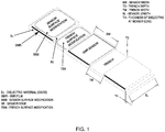
- FIG. 1 shows a cross-sectional drawing of a magnetic sensor according to embodiments of the present disclosure.
- a magnetic sensor includes a magnetic sensor element, such as a giant magnetoresistive (GMR) element (also referred to herein as a GMR film), on a support, such as a support composed of a dielectric material (also referred to herein as a dielectric layer (DL), which may be composed of an oxide such as silicon dioxide.
- the magnetic sensor element (GMR film) has a sensor width (SW) and a sensor length (SL).
- the magnetic sensor element (GMR film) includes a sensor surface modification (SSM) on a surface of the magnetic sensor element.
- SSM sensor surface modification
- the inter-element area Adjacent to the magnetic sensor element along the sensor length (SL) is an inter-element area (also referred to herein as a trench).
- the inter-element area (trench) has an inter-element area width (trench width (TW)) and an inter-element area depth (trench depth (TD)).
- the inter-element area has an inter-element area length (trench length) that is substantially the same as the sensor length (SL).
- the inter-element area is adjacent to the magnetic sensor element along the side (also referred to herein as the sensor edge (SE)) of the magnetic sensor element.
- the side of the magnetic sensor element (sensor edge (SE)) may have a side surface modification as described herein, such as a layer of a dielectric material (or a metal).
- the side surface modification has a thickness (TH).
- the inter-element area includes an inter-element area surface modification as described herein (also referred to herein as a trench surface modification (TSM)). As shown in FIG. 1 , more than one magnetic sensor may be arranged in series to form an array of magnetic sensors.
- TSM trench surface modification
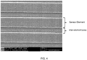
- FIG. 4 shows an SEM image of an enlargement of an arrangement of magnetic sensor elements and inter-element areas according to embodiments of the present disclosure.
- the magnetic sensor device includes a support.
- the support includes an array of magnetic sensors (e.g., an array of biosensors) disposed thereon.
- each magnetic sensor includes one or more magnetic sensor elements as described herein, and one or more inter-element areas as described herein. Aspects of the magnetic sensors are described further in the following sections.
- a magnetic sensor includes two or more magnetic sensor elements.
- the magnetic sensor elements are electrically connected to each other.
- the magnetic sensor elements are electrically connected to each other in series.
- the magnetic sensor elements may be electrically connected to each other in series by one or more electrodes.
- a current e.g., a sense current
- a current may flow through the magnetic sensor elements in series (e.g., sequentially).
- an array of magnetic sensor elements includes a plurality of magnetic sensor elements arranged in series and/or in parallel, which may include two or more magnetic sensor elements, including 3 or more, 4 or more, 6 or more, 8 or more, 10 or more, 15 or more, 20 or more, 25 or more, 30 or more, 40 or more, 50 or more, 75 or more, 100 or more, 125 or more, 150 or more, 175 or more, 200 or more, 225 or more, or 250 or more magnetic sensors arranged in series and/or in parallel.
- the array of magnetic sensor elements includes 100 or more magnetic sensor elements arranged in series and/or in parallel.
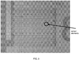
- FIG. 3 shows an enlargement of a magnetic sensor of FIG. 2 , which shows a plurality of magnetic sensor elements arranged in series and in parallel according to embodiments of the present disclosure.
- the magnetic sensor elements are arranged (e.g., arranged in series and/or in parallel as described above) such that the distance between adjacent magnetic sensor elements is 50 ⁇ m or less, such as 40 ⁇ m or less, including 30 ⁇ m or less, or 20 ⁇ m or less, or 10 ⁇ m or less, or 5 ⁇ m or less, or 4 ⁇ m or less, or 3 ⁇ m or less, or 2 ⁇ m or less, or 1 ⁇ m or less. In some cases, the distance between adjacent magnetic sensor elements is 2 ⁇ m.
- a magnetic sensor element may have dimensions in the range of 2 ⁇ m x 2 ⁇ m to 200 ⁇ m x 200 ⁇ m, including dimensions of 2 ⁇ m x 200 ⁇ m or less, such as 100 ⁇ m x 2 ⁇ m or less, for instance 2 ⁇ m x 100 ⁇ m or less, or 100 ⁇ m x 100 ⁇ m or less, or 10 ⁇ m x 10 ⁇ m or less, or 5 ⁇ m x 5 ⁇ m or less, or 3 ⁇ m x 3 ⁇ m or less, or 2 ⁇ m x 2 ⁇ m or less, or 1 ⁇ m x 1 ⁇ m or less.
- an inter-element area has dimensions in the range of 1 ⁇ m x 1 ⁇ m to 100 ⁇ m x 100 ⁇ m, including dimensions of 1 ⁇ m x 100 ⁇ m or less, such as 50 ⁇ m x 1 ⁇ m or less, for instance 1 ⁇ m x 50 ⁇ m or less, or 50 ⁇ m x 50 ⁇ m or less, or 5 ⁇ m x 5 ⁇ m or less, or 4 ⁇ m x 4 ⁇ m or less, or 3 ⁇ m x 3 ⁇ m or less, or 2 ⁇ m x 2 ⁇ m or less, or 1 ⁇ m x 1 ⁇ m or less.
- an electrode is composed of an electrically conductive material.
- the electrode is made of a conductive metal, e.g., copper, aluminum, palladium, a palladium alloy, a palladium oxide, platinum, a platinum alloy, a platinum oxide, ruthenium, a ruthenium alloy, a ruthenium oxide, silver, a silver alloy, a silver oxide, tin, a tin alloy, a tin oxide, titanium, a titanium alloy, a titanium oxide, tantalum, a tantalum alloy, a tantalum oxide, combinations thereof, and the like.
- the electrode is made of tantalum.
- the electrode is made of ruthenium.
- the electrode includes a layer of an electrically conductive material as described above.
- the electrode may include a layer of a conductive metal, such as tantalum.
- the electrode includes two or more layers of electrically conductive materials as described above.
- the electrode may include alternating layers of two different conductive metals, such as tantalum and ruthenium.
- a magnetic sensor includes a plurality of magnetic sensor elements.
- the magnetic sensor includes two or more magnetic sensor elements (e.g., two or more magnetic sensor elements arranged in series), as described above.
- the magnetic sensor device includes magnetic sensor elements arranged in series and additional magnetic sensor elements electrically connected in parallel to the first series of magnetic sensor arrays.
- the additional magnetic sensor elements may include two or more magnetic sensor elements arranged in series as described above.
- the magnetic sensor may include an arrangement of magnetic sensor elements where a plurality of magnetic sensor elements are electrically connected both in series and in parallel.
- the magnetic sensor device includes a support.
- the support includes an array of magnetic sensors (e.g., an array of biosensors) disposed thereon.
- the support has a thickness of 5 mm or less, such as 2 mm or less, including 1.6 mm or less, or 1.0 mm or less, or 0.5 mm or less, or 0.3 mm or less, or 0.2 mm or less.
- the support has a width of 20 mm or less, or 15 mm or less, such as 12 mm or less, including 10 mm or less, or 5 mm or less, or 2 mm or less.
- the support of the magnetic sensor device is shaped as a rectangular solid (although other shapes are possible), having a length ranging from 1 mm to 20 mm, such as 1 mm to 10 mm, including 1 mm to 5 mm; a width ranging from 1 mm to 20 mm, such as 1 mm to 10 mm, including 1 mm to 5 mm, or 1 mm to 3 mm; and a thickness ranging from 0.1 mm to 5 mm, such as 0.2 mm to 1 mm, including 0.3 mm to 0.5 mm.
- the magnetic sensor device includes an array of magnetic sensors (e.g., an array of biosensors).
- the array of magnetic sensors may have a variety of different configurations, e.g., with respect to magnetic sensor configuration.
- the subject magnetic sensors are arranged on a biochip (e.g., a biosensor chip).
- biochip or “biosensor chip” is meant a magnetic sensor device that includes an array of magnetic sensors (e.g., an array of biosensors).
- a biochip may include a magnetic sensor device that includes a support surface which displays two or more distinct arrays of magnetic sensors on the support surface.
- the magnetic sensor device includes a support surface with an array of magnetic sensors.
- An “array” includes any two-dimensional or substantially two-dimensional (as well as a three-dimensional) arrangement of addressable regions, e.g., spatially addressable regions.
- An array is "addressable” when it has multiple sensors positioned at particular predetermined locations (e.g., "addresses") on the array.
- Array features e.g., sensors
- Any given support may carry one, two, four or more arrays disposed on a front surface of the support. Depending upon the use, any or all of the arrays may be the same or different from one another and each may contain multiple distinct magnetic sensors.
- An array may contain one or more, including 2 or more, 4 or more, 8 or more, 10 or more, 50 or more, 100 or more, 250 or more, 500 or more, 750 or more, 1000 or more magnetic sensors.
- 64 magnetic sensors can be arranged into an 8 ⁇ 8 array
- 80 magnetic sensors can be arranged in an 8x10 array
- 90 sensors can be arranged in a 9x10 array.
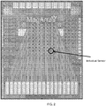
- FIG. 2 shows an image of an array of 80 magnetic sensors according to embodiments of the present disclosure.
- the magnetic sensors are arranged in the array in rows and columns of magnetic sensors.
- an array may include one or more rows of two or more magnetic sensors.
- an array includes 1 or more rows, such as 2 or more, or 3 or more, or 4 or more, or 5 or more, or 6 or more, or 7 or more, or 8 or more, or 9 or more, or 10 or more, or 12 or more, or 14 or more, or 16 or more, or 18 or more, or 20 or more, or 25 or more, or 30 or more, or 35 or more, or 40 or more, or 45 or more, or 50 or more rows of magnetic sensors.
- an array includes 1 or more columns, such as 2 or more, or 3 or more, or 4 or more, or 5 or more, or 6 or more, or 7 or more, or 8 or more, or 9 or more, or 10 or more, or 12 or more, or 14 or more, or 16 or more, or 18 or more, or 20 or more, or 25 or more, or 30 or more, or 35 or more, or 40 or more, or 45 or more, or 50 or more columns of magnetic sensors.
- 64 magnetic sensors can be arranged into an 8 ⁇ 8 array that includes 8 rows and 8 columns of magnetic sensors, or 80 magnetic sensors can be arranged in an 8x10 array that includes 10 rows and 8 columns of magnetic sensors.
- the magnetic sensors can be arranged into an array with an area of 10 cm 2 or less, or 9 cm 2 or less, 5 cm 2 or less, 4 cm 2 or less, e.g., 2 cm 2 or less, 1.2 cm 2 or less, 0.1 cm 2 or less, including 50 mm 2 or less, 20 mm 2 or less, such as 10 mm 2 or less, or even smaller.
- the magnetic sensors can be arranged into an array with an area of 15 mm 2 or less, such as 12.2 mm 2 or less (e.g., 3.2 mm x 3.8 mm). In some instances, the magnetic sensors are arranged into an array with an area of 20 mm 2 .
- the magnetic sensors may have a density in an array of 1 magnetic sensor per 2 mm 2 array area or less, such as 1 magnetic sensor per 1 mm 2 array area or less, or 1 magnetic sensor per 0.5 mm 2 array area, or 1 magnetic sensor per 0.2 mm 2 array area, or 1 magnetic sensor per 0.16 mm 2 array area, or 1 magnetic sensor per 0.14 mm 2 array area, or 1 magnetic sensor per 0.12 mm 2 array area, or 1 magnetic sensor per 0.1 mm 2 array area, or 1 magnetic sensor per 0.08 mm 2 array area, or 1 magnetic sensor per 0.05 mm 2 array area.
- the magnetic sensors may have a density in an array of 1 magnetic sensor per 0.16 mm 2 array area.
- magnetic biosensors with multiple magnetic sensor elements are dimensioned to cover a portion of the support which is contacted with a sample of biological molecules during an assay.
- the placement of the sample (e.g., biological molecules) onto individual sensors or inter-element areas may be performed by placing small droplets of a liquid sample with biological molecules onto certain regions of the support, or by placing a stamp coated with biological molecules into contact with the support.
- the area of the support coated by a sample of biological molecules and the area of a biosensor are substantially similar.
- the biosensor may have dimensions in the range of 10 ⁇ m x 10 ⁇ m to 1000 ⁇ m x 1000 ⁇ m, including dimensions of 10 ⁇ m x 1000 ⁇ m or less, such as 1000 ⁇ m x 10 ⁇ m or less, for instance 800 ⁇ m x 800 ⁇ m or less, or 400 ⁇ m x 400 ⁇ m or less, or 200 ⁇ m x 200 ⁇ m or less, or 180 ⁇ m x 180 ⁇ m or less, or 160 ⁇ m x 160 ⁇ m or less, or 140 ⁇ m x 140 ⁇ m or less, or 120 ⁇ m x 120 ⁇ m or less, or 100 ⁇ m x 100 ⁇ m or less, or 80 ⁇ m x 80 ⁇ m or less, or 50 ⁇ m x 50 ⁇ m or less, or 30 ⁇ m x 30 ⁇ m or less.
- a biosensor has dimensions of 140 ⁇ m x 140 ⁇ m or less, such as 120 ⁇ m x 120 ⁇ m or less
- magnetic biosensors with multiple magnetic sensor elements are spaced apart such that the number of biosensors per unit area is maximized, while still allowing individual biosensors to be contacted with separate droplets of a liquid sample containing biological molecules.
- the biosensors may be spaced a certain distance apart and separated by the inter-element areas as described herein.
- each magnetic sensor array may include one or more magnetic sensors having an analyte-specific probe bound to a surface of the magnetic sensor or the inter-element area.
- each sensor or inter-element area may have the same or different analyte-specific probe associated with its surface.
- a magnetic sensor array may include two or more distinct magnetic sensors or inter-element areas each configured to specifically detect the same analyte.
- a magnetic sensor array may include two or more distinct magnetic sensors or distinct inter-element areas each configured to specifically detect a different analyte.
- the magnetic sensor devices include magnetic sensors or inter-element areas that are free of any analyte-specific probes, such that the surface of the magnetic sensor or inter-element area is functionalized to bind directly to the analyte.
- the magnetic sensor or inter-element area includes a blocking layer disposed over the surface of the magnetic sensor or inter-element area.
- the blocking layer may be configured to inhibit the binding of any analyte-specific probes or analyte to the surface of the magnetic sensor (e.g., where such blocked magnetic sensors may serve as sources of reference or control electrical signals) or inter-element area (e.g., where such blocked inter-element areas may serve as sources of reference or control electrical signals).
- the magnetic sensor device includes two or more magnetic sensor arrays disposed on a support.
- the magnetic sensor device includes two or more magnetic sensor arrays.
- each magnetic sensor array may have one or more magnetic sensors or inter-element areas with each magnetic sensor or inter-element area configured to detect the same or different analytes.
- each magnetic sensor array on the magnetic sensor device may be configured to detect the same set or different sets of analytes.
- a magnetic sensor device may include two or more distinct magnetic sensor arrays each configured to specifically detect the same set of analytes.
- a magnetic sensor device may include two or more distinct magnetic sensor arrays each configured to specifically detect a different set of analytes.
- Electronic communication elements e.g., conductive leads, may be present which are configured to electronically couple the magnetic sensors to components of the system, such as processors, displays, etc.
- a given magnetic sensor device may include a variety of other components in addition to the magnetic sensor array. Additional magnetic sensor device components may include, but are not limited to: signal processing components, power sources, fluid handling components, wired or wireless communication components, etc.
- the magnetic sensor device is configured to produce a detectable signal from a minimum amount of sample. In some instances, the magnetic sensor device is configured to produce a detectable signal from a sample size of 10 mL or less, or 5mL or less, or 3 mL or less, or 1 mL or less, such as 500 ⁇ L or less, including 100 ⁇ L or less, for example 50 ⁇ L or less, or 25 ⁇ L or less, or 10 ⁇ L or less. As such, in some cases, the inter-element areas may be configured to receive a minimum amount of sample needed to produce a detectable signal.
- the inter-element areas may be configured to receive a sample of 10 mL or less, or 5 mL or less, or 3 mL or less, or 1 mL or less, such as 500 ⁇ L or less, including 100 ⁇ L or less, for example 50 ⁇ L or less, or 25 ⁇ L or less, or 10 ⁇ L or less, or 5 ⁇ L or less, or 1 ⁇ L or less.
- the magnetic sensor device is configured to connect to a system for detecting the presence of an analyte in a sample. Accordingly, in certain embodiments, the magnetic sensor device does not include a magnetic field source. The magnetic field source may be included in the system for detecting the presence of an analyte in the sample and, thus not included in the magnetic sensor device itself.
- the assay protocol may include operably coupling the magnetic sensor device to the system for detecting the presence of an analyte in the sample.
- the magnetic sensor device may be operably coupled to an activation and signal processing unit of the system, as described herein.
- the magnetic sensor device may include one or more electrical contacts configured to electrically connect the magnetic sensor device to the system, such as to the activation and signal processing unit of the system. The electrical contacts may be arranged along an edge of the magnetic sensor device.
- the magnetic sensor device includes a programmable memory.
- the programmable memory is configured to store information, such as information including, but not limited to: calibration data (e.g., calibration data for each magnetic sensor and/or each magnetic sensor array); a record of how the magnetic sensors have been prepared with surface functionalization molecules prior to the assay; a record of completed assay steps; a record about which sample was measured; a record of the measurement results; and the like.
- a barcode may be used instead of, or in addition to, the programmable memory.
- information associated with the magnetic sensor device may be stored and retrieved from an information system separate from the magnetic sensor device, such as the activation and signal processing unit of the system.
- each magnetic sensor may include one or more magnetic sensor elements.
- magnetic sensors are sensors configured to detect the presence of nearby magnetic labels without any direct physical contact between the magnetic sensor and the magnetic label.
- the magnetic sensors are configured to detect the presence of an analyte in a sample.
- a magnetic label may be bound, either directly or indirectly, to an analyte, which in turn may be bound, either directly or indirectly, to the magnetic sensor. If the bound magnetic label is positioned within the detection range of the magnetic sensor, then the magnetic sensor may provide a signal indicating the presence of the bound magnetic label, and thus indicating the presence of the analyte.
- the magnetic sensors have a detection range from 1 nm to 1000 nm from the surface of the magnetic sensor, such as from 1 nm to 800 nm, including from 1 nm to 500 nm, such as from 1 nm to 300 nm, including from 1 nm to 100 nm from the surface of the magnetic sensor.
- a minimization of the detection range of the sensors may facilitate detection of specifically bound analytes while minimizing detectable signals from analytes not of interest.
- detection range is meant the distance from the surface of the magnetic sensor where the presence of a magnetic label will induce a detectable signal in the magnetic sensor.
- magnetic labels positioned close enough to the surface of the magnetic sensor to be within the detection range of the magnetic sensor will induce a detectable signal in the magnetic sensor.
- magnetic labels positioned at a distance from the surface of the magnetic sensor that is greater than the detection range of the magnetic sensor will not induce a detectable or non-negligible signal in the magnetic sensor.
- a magnetic label may have a magnetic flux that is proportional to 1/r 3 , where r is the distance between the magnetic sensor and the magnetic label. Thus, only those magnetic labels that are positioned in close proximity (e.g., within the detection range of the magnetic sensor) will induce a detectable signal in the magnetic sensor.
- the surface of the magnetic sensor is functionalized to bind directly to an analyte or a magnetic label.
- the surface of the magnetic sensor may be functionalized to provide for covalent binding or non-covalent association between the analyte or the magnetic label and magnetic sensor, including, but not limited to, non-specific adsorption, binding based on electrostatic interactions (e.g., ion-ion pair interactions), hydrophobic interactions, hydrogen bonding interactions, and the like.
- the surface of the magnetic sensor or the inter-element area includes an analyte-specific probe (e.g., a surface capture ligand) that specifically binds to an analyte.
- the analyte-specific probe may be bound to the surface of the magnetic sensor or the inter-element area.
- a cationic polymer such as polyethyleneimine (PEI) can be used to nonspecifically bind charged antibodies to the surface via physiabsorption.
- PEI polyethyleneimine
- a covalent chemistry can be used utilizing free amines or free thiol groups on the analyte-specific probe to covalently bind the analyte-specific probe to the surface of the magnetic sensor or the inter-element area.
- an N-hydroxysuccinimide (NHS) to 1-ethyl-3-(3-dimethylaminopropyl) carbodiimide (EDC) coupling system may be used to covalently bind the analyte-specific probe to the surface of the magnetic sensor or the inter-element area.
- NHS N-hydroxysuccinimide
- EDC 1-ethyl-3-(3-dimethylaminopropyl) carbodiimide
- the analyte-specific probe may include one member of a specific binding pair.
- suitable specific binding pairs include, but are not limited to: a member of a receptor/ligand pair; a ligand-binding portion of a receptor; a member of an antibody/antigen pair; an antigen-binding fragment of an antibody; a hapten; a member of a lectin/carbohydrate pair; a member of an enzyme/substrate pair; biotin/avidin; biotin/streptavidin; digoxin/antidigoxin; and the like.
- the surface of the magnetic sensor or the inter-element area includes an antibody that specifically binds to an analyte of interest.
- contacting the magnetic sensor or the inter-element area with an assay composition that includes the analyte of interest may result in binding of the analyte to the analyte-specific probe (e.g., antibody) bound to the surface of the magnetic sensor or the inter-element area.
- analyte-specific probe e.g., antibody
- the magnetic sensor is configured to generate an electrical signal in response to a magnetic label in proximity to a surface of the magnetic sensor.
- the magnetic sensors may be configured to detect changes in the resistance of the magnetic sensor induced by changes in the local magnetic field.
- binding of a magnetic label e.g., a magnetic nanoparticle label
- the magnetic labels near the magnetic sensor may be magnetized.
- the local magnetic field of the magnetized magnetic labels may induce a detectable change in the resistance of the underlying magnetic sensor.
- the presence of the magnetic labels can be detected by detecting changes in the resistance of the magnetic sensor.
- the magnetic labels near the magnetic sensor may be present in an inter-element area such as bound to an inter-element area as described herein. In certain embodiments, the magnetic labels near the magnetic sensor may be present in an inter-element area such as bound to a side surface of a magnetic sensor element as described herein.
- the magnetic sensors are configured to detect changes in resistance of 1 Ohm or less, such as 500 mOhm or less, including 100 mOhm or less, or 50 mOhm or less, or 25 mOhm or less, or 10 mOhm or less, or 5 mOhm or less, or 1 mOhm or less.
- the change in resistance may be expressed in parts per million (PPM) relative to the original sensor resistance, such as a change in resistance of 2 PPM or more, or 20 PPM or more, or 200 PPM or more, or 400 PPM or more, or 600 PPM or more, or 1000 PPM or more, or 2000 PPM or more, or 4000 PPM or more, or 6000 PPM or more, or 10,000 PPM or more, or 20,000 PPM or more, or 40,000 PPM or more, or 60,000 PPM or more, or 100,000 PPM or more, or 200,000 PPM or more.
- PPM parts per million
- the magnetic sensor is a multilayer thin film structures.
- the sensors may include alternating layers of a ferromagnetic material and a non-magnetic material.
- the ferromagnetic material may include, but is not limited to, Permalloy (NiFe), iron cobalt (FeCo), nickel iron cobalt (NiFeCo), nickel oxide (NiO), cobalt oxide (CoO), nickel cobalt oxide (NiCoO), ferric oxide (Fe 2 O 3 ), CoFeB, Ru, PtMn, combinations thereof, and the like.
- the non-magnetic material is an insulating layer, such as, but not limited to, MgO, alumina, and the like.
- the ferromagnetic layers have a thickness of 1 nm to 10 nm, such as 2 nm to 8 nm, including 3 nm to 4 nm. In some instances, the non-magnetic layer has a thickness of 0.2 nm to 5 nm, such as 1 nm to 3 nm, including 1.5 nm to 2.5 nm, or 1.8 nm to 2.2 nm.
- the magnetic sensor element is a spin valve magnetoresistive element.
- the spin valve element is a multilayer structure that includes a first ferromagnetic layer, a non-magnetic layer disposed on the first ferromagnetic layer, and a second ferromagnetic layer disposed on the non-magnetic layer.
- the first ferromagnetic layer may be configured to have its magnetization vector fixed in a certain direction.
- the first ferromagnetic layer is called the "pinned layer”.
- the spin valve element includes a pinned layer with a magnetization substantially parallel to a width of the magnetic sensor element, as described above.
- the second ferromagnetic layer may be configured such that its magnetization vector can rotate freely under an applied magnetic field. In some cases, the second ferromagnetic layer is called the "free layer”.
- the electrical resistance of a spin valve element depends on the relative orientation of the magnetization vector of the free layer to that of the pinned layer. When the two magnetization vectors are parallel, the resistance is the lowest; when the two magnetization vectors are antiparallel, the resistance is the highest.
- the relative change of resistance is called the magnetoresistance (MR) ratio.
- MR magnetoresistance
- a spin valve element has a MR ratio of 1% to 20%, such as 3% to 15 %, including 5% to 12%. In some cases, the MR ratio of a spin valve element is 10% or more in a small magnetic field, e.g., 100 Oe. Changes in the resistance of the spin valve element due to the presence of magnetic labels near the surface of the spin valve element may be detected, as described above.
- the signal from the spin valve element due to the magnetic label depends on the distance between the magnetic label and the free layer of the spin valve element.
- the voltage signal from a magnetic label decreases as the distance from the center of the magnetic label to the mid-plane of the free layer increases.
- the free layer in the spin valve element is positioned at the surface of the spin valve element. Positioning the free layer at the surface of the spin valve element may minimize the distance between the free layer and any bound magnetic labels, which may facilitate detection of the magnetic labels.
- the spin valve element may include a passivation layer disposed on one or more of the spin valve element surfaces.
- the passivation layer has a thickness of 60 nm or less, such as 50 nm or less, including 40 nm or less, 30 nm or less, 20 nm or less, 10 nm or less.
- the passivation layer may have a thickness of 1 nm to 10 nm, such as from 1 nm to 5 nm, including from 1 nm to 3 nm.
- the passivation layer includes gold, tantalum, SiO 2 , Si 3 N 4 , combinations thereof, and the like.
- the magnetic sensor element is a magnetic tunnel junction (MTJ) magnetoresistive element (also referred to herein as an MTJ element).
- the MTJ element includes a multilayer structure that includes a first ferromagnetic layer, an insulating layer disposed on the first ferromagnetic layer, and a second ferromagnetic layer disposed on the insulating layer.
- the insulating layer may be a thin insulating tunnel barrier, and may include alumina, MgO, and the like.
- electron tunneling between the first and the second ferromagnetic layers depends on the relative magnetization of the two ferromagnetic layers. For example, in certain embodiments, the tunneling current is high when the magnetization vectors of the first and second ferromagnetic layers are parallel and the tunneling current is low when the magnetization vectors of the first and second ferromagnetic layers antiparallel.
- a MTJ element has a magnetoresistance ratio (MR) of 1% to 300%, such as 10% to 250%, including 25% to 200%. Changes in the resistance of the MTJ element due to the presence of magnetic labels near the surface of the MTJ element may be detected, as described above.
- the MTJ element has an MR of 50% or more, or 75% or more, or 100% or more, or 125% or more, or 150% or more, or 175% or more, or 200% or more, or 225% or more, or 250% or more, or 275% or more, or 200% or more.
- the MTJ element may have an MR of 225% or more.
- the second ferromagnetic layer (e.g., the layer of the MTJ element positioned at the surface of the MTJ element) includes two of more layers.
- the second ferromagnetic layer may include a first layer, a second layer disposed on the first layer, and a third layer disposed on the second layer.
- the first layer is a thin ferromagnetic layer (e.g., NiFe, CoFe, CoFeB, and the like).
- the thin metallic layer may have a thickness of 6 nm or less, such as 5 nm or less, including 4 nm or less, 3 nm or less, 2 nm or less, or 1 nm or less, or 0.5 nm or less.
- the second layer may include a conductive metal, e.g., copper, aluminum, palladium, a palladium alloy, a palladium oxide, platinum, a platinum alloy, a platinum oxide, ruthenium, a ruthenium alloy, a ruthenium oxide, silver, a silver alloy, a silver oxide, tin, a tin alloy, a tin oxide, titanium, a titanium alloy, a titanium oxide, tantalum, a tantalum alloy, a tantalum oxide, combinations thereof, and the like.
- a conductive metal e.g., copper, aluminum, palladium, a palladium alloy, a palladium oxide, platinum, a platinum alloy, a platinum oxide, ruthenium, a ruthenium alloy, a ruthenium oxide, silver, a silver alloy, a silver oxide, tin, a tin alloy, a tin oxide, titanium, a titanium alloy, a titanium oxide, tantalum,
- the second layer may have a thickness of 2 nm or less, such as 0.5 nm or less, including 0.4 nm or less, 0.3 nm or less, 0.2 nm or less, or 0.1 nm or less.
- the third layer may include a ferromagnetic material such as, but not limited to, NiFe, CoFe, CoFeB, and the like.
- the third layer may have a thickness of 6 nm or less, such as 5 nm or less, including 4 nm or less, 3 nm or less, 2 nm or less, or 1 nm or less, or 0.5 nm or less.
- the MTJ element is configured such that the distance between an associated magnetic label and the top surface of the free layer ranges from 5 nm to 1000 nm, or 10 nm to 800 nm, such as from 20 nm to 600 nm, including from 40 nm to 400 nm, such as from 60 nm to 300 nm, including from 80 nm to 250 nm.
- the MTJ element may include a passivation layer disposed on one or more of the MTJ element surfaces.
- the passivation layer has a thickness of 60 nm or less, such as 50 nm or less, including 40 nm or less, 30 nm or less, 20 nm or less, 10 nm or less.
- the passivation layer may have a thickness of 1 nm to 50 nm, such as from 1 nm to 40 nm, including from 1 nm to 30 nm, or form 1 nm to 20 nm.
- the passivation layer has a thickness of 30 nm.
- the passivation layer includes gold, tantalum, a tantalum alloy, a tantalum oxide, aluminum, an aluminum alloy, an aluminum oxide, SiO 2 , Si 3 N 4 , ZrO 2 , combinations thereof, and the like.
- a passivation layer with a thickness as described above facilitates a maximization in signal detected from magnetic labels specifically bound to the sensor surface or the inter-element area while minimizing the signal from magnetic labels that are not specifically bound.
- a MTJ element has dimensions ranging from 1 ⁇ m x 1 ⁇ m to 200 ⁇ m x 200 ⁇ m, including dimensions of 1 ⁇ m x 200 ⁇ m or less, such as 200 ⁇ m x 1 ⁇ m or less, for instance 150 ⁇ m x 10 ⁇ m or less, or 120 ⁇ m x 5 ⁇ m or less, or 120 ⁇ m x 0.8 ⁇ m or less, or 0.8 ⁇ m x 120 ⁇ m or less, or 100 ⁇ m x 0.7 ⁇ m or less, or 100 ⁇ m x 0.6 ⁇ m or less, or 100 ⁇ m x 0.5 ⁇ m or less, or 10 ⁇ m x 0.6 ⁇ m or less, or 10 ⁇ m x 0.5 ⁇ m or less.
- a MTJ element has dimensions of 120 ⁇ m x 0.8 ⁇ m or less, such as 2.0 ⁇ m x 0.8 ⁇ m.
- Magnetic tunnel junction (MTJ) detectors are further described in U.S. Application Publication No. 2009/0104707 . Detectors are further described in U.S. Patent No. 7,906,345 .
- the magnetic sensor device may be configured to include one or more magnetic sensing areas.
- a magnetic sensing area may correspond to the area of the device where an array of magnetic sensors (e.g., an array of biosensors) is positioned.
- the magnetic sensing area may be an area on the surface of the device that is exposed to the sample during use, and which has an array of magnetic sensors (e.g., an array of biosensors) as described above.
- the magnetic sensing area may be configured to include a fluid reservoir.
- the fluid reservoir may be any of a variety of configurations, where the fluid reservoir is configured to hold a sample in contact with the magnetic sensor arrays. Accordingly, configurations of the fluid reservoirs may include, but are not limited to: cylindrical well configurations, square well configurations, rectangular well configurations, round bottom well configurations, and the like.
- the fluid reservoirs may include walls that separate one fluid reservoir from adjacent fluid reservoirs. The walls may be substantially vertical with respect to the surface of the reservoir plate. In some cases, the walls of each fluid reservoir define a volume of space that may receive a volume of sample equal to or less than the volume of space defined by the fluid reservoir.
- a fluid reservoir has a volume of 10 mL or less, or 5mL or less, or 3 mL or less, or 1 mL or less, such as 500 ⁇ L or less, including 100 ⁇ L or less, for example 50 ⁇ L or less, or 25 ⁇ L or less, or 10 ⁇ L or less, which is sufficient to contain a sample volume of an equal or lesser volume.
- the systems include a magnetic sensor device, and a magnetic field source.
- the magnetic sensor device includes a support having two or more arrays of magnetic sensors (e.g., arrays of biosensors) positioned thereon.
- the system may be configured to obtain signals from each array of magnetic sensors indicating whether one or more analytes is present in each sample.
- the system includes a magnetic field source.
- the magnetic field source may be configured to apply a magnetic field to the magnetic sensor device (e.g., the magnetic sensor arrays) sufficient to produce a DC and/or AC field in the assay sensing area (e.g. in the area where the magnetic sensor arrays are positioned during signal acquisition).
- the magnetic field source is configured to produce a magnetic field with a magnetic field strength of 1 Oe or more, or 5 Oe or more, or 10 Oe or more, or 20 Oe or more, or 30 Oe or more, or 40 Oe or more, or 50 Oe or more, or 60 Oe or more, or 70 Oe or more, or 80 Oe or more, or 90 Oe or more, or 100 Oe or more.
- the magnetic field source may be positioned such that a magnetic field is produced in the area where the magnetic sensor arrays are positioned when the magnetic sensor device is in use.
- the magnetic field source is configured to generate a uniform, controllable magnetic field around the set of fluid reservoirs on the reservoir plate where an assay is being performed.
- the magnetic field source may include one or more, such as two or more, three or more, four or more magnetic field generating components.
- the magnetic field source may include one or more electromagnets, such as coil electromagnets.
- the coil electromagnets may include wire-wound coils.
- the magnetic field source may include two electromagnets arranged in a Helmholtz coil geometry.
- Embodiments of the systems further include computer-based systems.
- the systems may be configured to qualitatively and/or quantitatively assess binding interactions as described above.
- a "computer-based system” refers to the hardware, software, and data storage components used to analyze the signals from the magnetic sensors.
- the hardware of the computer-based systems may include a central processing unit (CPU), inputs, outputs, and data storage components. Any of a variety of computer-based systems is suitable for use in the subject systems.
- the data storage components may include any computer readable medium that includes a device for recording signals from the magnetic sensor arrays, or an accessible memory component that can store signals from the magnetic sensor arrays.
- Record data programming or other information on a computer readable medium refers to a process for storing information, using any such methods as known in the art. Any convenient data storage structure may be chosen, depending on the method used to access the stored information. A variety of data processor programs and formats can be used for storage, e.g. word processing text file, database format, etc.
- the system includes an activation and signal processing unit.
- the activation and signal processing unit may be configured to operably couple to the magnetic sensor device.
- the activation and signal processing unit is electrically coupled to the magnetic sensor device.
- the activation and signal processing unit may be electrically coupled such as to provide bi-directional communication to and from the magnetic sensor device.
- the activation and signal processing unit may be configured to provide power, activation signals, etc. to components of the magnetic sensor device, such as, but not limited to the magnetic sensor arrays.
- the activation and signal processing unit may include an activation signal generator.
- the activation signal generator may be configured to provide power, activation signals, etc. to components of the analyte detection device, such as, but not limited to the magnetic sensor arrays.
- the activation and signal processing unit is configured to apply a voltage across the magnetic sensor arrays ranging from 1 mV to 10 V, such as 100 mV to 5 V, including 200 mV to 1 V, for example, 300 mV to 500 mV. In some cases, the activation and signal processing unit is configured to apply a voltage across the magnetic sensor arrays of 500 mV.
- the activation and signal processing unit may be configured to receive signals from the magnetic sensor device, such as from the magnetic sensor arrays of the magnetic sensor device.
- the signals from the magnetic sensor arrays of the magnetic sensor device may be used to detect the presence of one or more analytes in the samples.
- the activation and signal processing unit may include a processor configured to output an analyte detection result in response to receiving signals from the magnetic sensor arrays.
- the processor of the activation and signal processing unit may be configured to receive signals from the magnetic sensor device, process the signals according to a predetermined algorithm, obtain a result related to the presence of one or more analytes in the samples, and output the result to a user in a human-readable or an audible format.
- a "processor” references any hardware and/or software combination that will perform one or more programmed functions.
- any processor herein may be a programmable digital microprocessor such as available in the form of an electronic controller, mainframe, server or personal computer (e.g., desktop or portable).
- suitable programming can be communicated from a remote location to the processor, or previously saved in a computer program product (such as a portable or fixed computer readable storage medium, whether magnetic, optical or solid-state device based).
- a magnetic medium, optical disk or solid-state memory device may carry the programming, and can be read by a suitable reader communicating with the processor.
- the subject systems are configured to modulate the current applied to the magnetic sensor arrays (e.g., the sense current).
- the subject systems may also be configured to modulate the magnetic field generated by the magnetic field source. Modulating the sense current and the magnetic field may facilitate a minimization in signal noise, and thus a maximization in the signal to noise ratio. Additional aspects of modulating the sense current and the magnetic field are described in more detail in U.S. Application Publication No. 2011/0027901 .
- Embodiments of the subject systems may also include the following components: (a) a wired or wireless communications module configured to transfer information between the system and one or more users, e.g., via a user computer, as described below; and (b) a processor for performing one or more tasks involved in the qualitative and/or quantitative analysis of the signals from the magnetic sensors.
- a computer program product includes a computer-usable medium having control logic (e.g., a computer software program, including program code) stored therein.
- the control logic when executed by the processor of the computer, causes the processor to perform functions described herein.
- some functions are implemented primarily in hardware using, for example, a hardware state machine. Implementation of the hardware state machine so as to perform the functions described herein may be accomplished using any convenient method and techniques.
- the systems may include a number of additional components, such as, but not limited to: data output devices, e.g., monitors, speakers, etc.; data input devices, e.g., interface ports, buttons, switches, keyboards, etc.; fluid handling components, e.g., microfluidic components; power sources; power amplifiers; wired or wireless communication components; etc.
- the systems may include fluid handling components, such as microfluidic fluid handling components.
- the microfluidic fluid handling components are configured to deliver a fluid to the inter-element areas.
- the fluid includes one or more of the following: an assay composition, a sample, a magnetic label, a capture probe, a reagent, and the like.
- the microfluidic fluid handling components are configured to deliver small volumes of fluid, such as 1 mL or less, such as 500 ⁇ L or less, including 100 ⁇ L or less, for example 50 ⁇ L or less, or 25 ⁇ L or less, or 10 ⁇ L or less.
- the system is a high-sensitivity analyte detector.
- high-sensitivity is meant that the system is configured to detect an analyte in a sample, where the concentration of the analyte in the sample is low.
- the system is configured to produce a detectable signal indicating the presence of an analyte of interest in a sample where the concentration of the analyte in the sample is 1 ⁇ M or less, such as 100 nM or less, or 10 nM or less, or 1 nM or less, including 100 pM or less, or 10 pM or less, or 1 pM or less, for example 500 fM or less, or 250 fM or less, or 100 fM or less, or 50 fM or less, or 25 fM or less, such as 10 fM or less, or 5 fM or less, or 1 fM or less.
- the system may be configured to have a detection limit, e.g., a lower limit of quantitation (LLOQ), of 1 ⁇ M or less, such as 100 nM or less, or 10 nM or less, or 1 nM or less, including 100 pM or less, or 10 pM or less, or 1 pM or less, for example 500 fM or less, or 250 fM or less, or 100 fM or less, or 50 fM or less, or 25 fM or less, such as 10 fM or less, or 5 fM or less, or 1 fM or less.
- LLOQ lower limit of quantitation
- the systems include a display.
- the display may be configured to provide a visual indication of an analyte detection result obtained from the activation and signal processing unit, as described above.
- the display may be configured to display a qualitative analyte detection result.
- the qualitative display may be configured to display qualitative indicators to a user that a sample includes or does not include a specific analyte of interest.
- the display may be configured to display an analyte detection result, where the analyte detection result is a quantitative result, e.g., a quantitative measurement of the concentration of an analyte in a sample.
- the system may include a display configured to display the quantitative analyte detection result.
- the magnetic sensor device optionally includes a programmable memory, which prior to and during the use of the magnetic sensor device can be programmed with relevant information such as: calibration data for each individual sensor; a record of how the biochip has been prepared with surface functionalization molecules prior to the assay; a record of all completed assay steps; a record about which sample was measured; a record of the measurement results; and the like.
- relevant information such as: calibration data for each individual sensor; a record of how the biochip has been prepared with surface functionalization molecules prior to the assay; a record of all completed assay steps; a record about which sample was measured; a record of the measurement results; and the like.
- aspects of the present disclosure also include a method for evaluating whether an analyte is present in a sample.
- the method includes contacting a magnetic sensor device with a sample to generate a signal.
- the method includes evaluating whether the analyte is present in each sample based on the signal.
- Embodiments of the methods are directed to evaluating whether an analyte is present in a sample, e.g., determining the presence or absence of one or more analytes in a sample.
- the presence of one or more analytes in the sample may be determined qualitatively or quantitatively.
- Qualitative determination includes determinations in which a simple yes/no result with respect to the presence of an analyte in the sample is provided to a user.
- Quantitative determination includes both semi-quantitative determinations in which a rough scale result, e.g., low, medium, high, is provided to a user regarding the amount of analyte in the sample and fine scale results in which an exact measurement of the concentration of the analyte is provided to the user.
- a rough scale result e.g., low, medium, high
- the methods include the uniplex analysis of an analyte in a sample.
- uniplex analysis is meant that a sample is analyzed to detect the presence of one analyte in the sample.
- a sample may include a mixture of an analyte of interest and other molecular entities that are not of interest.
- the methods include the uniplex analysis of the sample to determine the presence of the analyte of interest in the sample mixture.
- Certain embodiments include the multiplex analysis of two or more analytes in a sample.
- multiplex analysis is meant that the presence of two or more distinct analytes, in which the two or more analytes are different from each other, is determined.
- analytes may include detectable differences in their molecular structure, sequence, and the like.
- the number of analytes is greater than 2, such as 4 or more, 6 or more, 8 or more, etc., up to 20 or more, e.g., 50 or more, including 100 or more, or 1000 or more distinct analytes.
- the methods include the multiplex analysis of 2 to 1000 distinct analytes, such as 4 to 500 distinct analytes, including 4 to 200 distinct analytes, or 4 to 100 distinct analytes, or 4 to 50 distinct analytes, or 4 to 20 distinct analytes.
- several multiplex assays may be conducted in parallel substantially simultaneously.
- the methods are wash-free methods of evaluating the presence of one or more analytes in a sample.
- wash-free is meant that no washing step is performed following reagent and/or sample contact with a magnetic sensor. As such, no step is performed during the assays of these embodiments in which unbound reagent (e.g., unbound magnetic labels) or unbound sample is removed from the magnetic sensor surface.
- the methods may include sequential contact of one or more distinct reagents and/or samples to a magnetic sensor surface, at no point during the assay is the sample surface contacted with a fluid in a manner that removes unbound reagent or sample from the magnetic sensor surface.
- no washing step is performed following contact of the magnetic sensor surface with a sample.
- the method does not include a washing step following contact of the magnetic sensor surface with a magnetic label.
- no washing step is performed following contact of the magnetic sensor surface with a capture probe.
- the wash step does not substantially change the signal from the magnetic sensor.
- the wash step may not result in a substantial change in the signal from the magnetic sensor because, in some instances, unbound magnetic labels do not have a substantially detectable signal as described herein.
- the wash step results in a signal change of 25% or less, such as 20% or less, or 15% or less, or 10% or less or 5% or less, or 4% or less, or 3% or less, or 2% or less, or 1% or less.
- the wash step results in a decrease in the signal from the magnetic sensor of 25% or less, such as 20% or less, or 15% or less, or 10% or less or 5% or less, or 4% or less, or 3% or less, or 2% or less, or 1% or less.
- aspects of the methods may also include obtaining a real-time signal from the magnetic sensor device.
- embodiments of the method include obtaining a real-time signal from the magnetic sensor arrays.
- real-time is meant that a signal is observed as it is being produced or immediately thereafter.
- a real-time signal is obtained from the moment of its initiation and is obtained continuously over a given period of time.
- certain embodiments include observing the evolution in real time of the signal associated with the occurrence of a binding interaction of interest (e.g., the binding of the analyte of interest to the magnetic sensor or the inter-element area and/or binding of a magnetic label to the analyte of interest).
- the real-time signal may include two or more data points obtained over a given period of time, where in certain embodiments the signal obtained is a continuous set of data points (e.g., in the form of a trace) obtained continuously over a given period of time of interest.
- the time period of interest may vary, ranging in some instances from 0.5 min to 60 min, such as 1 min to 30 min, including 1 min to 15 min, or 1 min to 10 min.
- the time period may begin at the moment of initiation of the real-time signal and may continue until the magnetic sensor reaches a maximum or saturation level (e.g., where all the analyte binding sites on the magnetic sensor are occupied).
- the time period begins when a sample is contacted with the magnetic sensor.
- the time period may begin prior to contacting the sample with the magnetic sensor, e.g., to record a baseline signal before contacting sample to the magnetic sensor.
- the number of data points in the signal may also vary, where in some instances, the number of data points is sufficient to provide a continuous stretch of data over the time course of the real-time signal.
- continuous is meant that data points are obtained repeatedly with a repetition rate of 1 data point per minute or more, such as 2 data points per minute or more, including 5 data points per minute or more, or 10 data points per minute or more, or 30 data points per minute or more, or 60 data points per minute or more (e.g., 1 data point per second or more), or 2 data points per second or more, or 5 data points per second or more, or 10 data points per second or more, or 20 data points per second or more, or 50 data points per second or more, or 75 data points per second or more, or 100 data points per second or more.
- 1 data point per minute or more such as 2 data points per minute or more, including 5 data points per minute or more, or 10 data points per minute or more, or 30 data points per minute or more, or 60 data points per minute or more (e.g., 1 data point per second or more), or 2 data points per second or more, or 5 data points per second or more, or 10 data points per second or more, or 20 data points per second or more, or 50 data points per
- the real-time signal is a real-time analyte-specific signal.
- a real-time analyte-specific signal is a real-time signal as described above that is obtained only from the specific analyte of interest.
- unbound analytes and unbound magnetic labels do not produce a detectable signal.
- non-specifically bound analytes and non-specifically bound magnetic labels do not produce a detectable signal.
- the real-time signal that is obtained is only from the specific magnetically-labeled analyte of interest bound to the magnetic sensor or inter-element area and substantially no signal is obtained from unbound or non-specifically bound magnetic labels or other reagents (e.g., analytes not specifically bound to the sensor).
- the signal is observed while the assay device is in a wet condition.
- wet or “wet condition” is meant that the assay composition (e.g., an assay composition that includes a sample, a magnetic label, and a capture probe) is still in contact with the surface of the magnetic sensor.
- the use of magnetic labels and magnetic sensors, as described above facilitates "wet” detection because the signal induced in the magnetic sensor by the magnetic label decreases as the distance between the magnetic label and the surface of the magnetic sensor increases.
- the use of magnetic labels and magnetic sensors may facilitate "wet” detection because the magnetic field generated by the magnetic labels decreases as the distance between the magnetic label and the surface of the magnetic sensor increases.
- the magnetic field of the magnetic label bound to the surface-bound analyte significantly exceeds the magnetic field from the unbound magnetic labels dispersed in solution.
- a real-time analyte-specific signal may be obtained only from the specific magnetically-labeled analyte of interest bound to the magnetic sensor and substantially no signal may be obtained from unbound magnetic labels dispersed in solution (e.g., not specifically bound to the sensor).
- the unbound magnetic labels dispersed in solution may be at a greater distance from the surface of the magnetic sensor and may be in Brownian motion, which may reduce the ability of the unbound magnetic labels to induce a detectable change in the resistance of the magnetic sensor.
- the method includes contacting a magnetic sensor array with an assay composition that includes a sample.
- the magnetic sensor array may then be contacted with a magnetic label and a capture probe configured to bind to the magnetic label.
- a signal is obtained from the sensor to detect the presence of the analyte in the sample.
- Samples that may be assayed in the subject methods may vary, and include both simple and complex samples.
- Simple samples are samples that include the analyte of interest, and may or may not include one or more molecular entities that are not of interest, where the number of these non-interest molecular entities may be low, e.g., 10 or less, 5 or less, etc.
- Simple samples may include initial biological or other samples that have been processed in some manner, e.g., to remove potentially interfering molecular entities from the sample.
- complex sample is meant a sample that may or may not have the analytes of interest, but also includes many different proteins and other molecules that are not of interest.
- the complex sample assayed in the subject methods is one that includes 10 or more, such as 20 or more, including 100 or more, e.g., 10 3 or more, 10 4 or more (such as 15,000; 20,000 or 25,000 or more) distinct (i.e., different) molecular entities, that differ from each other in terms of molecular structure.
- the samples of interest are biological samples, such as, but not limited to, urine, blood, serum, plasma, saliva, perspiration, feces, cheek swabs, cerebrospinal fluid, cell lysate samples, and the like.
- the sample can be a biological sample or can be extracted from a biological sample derived from humans, animals, plants, fungi, yeast, bacteria, tissue cultures, viral cultures, or combinations thereof using conventional methods for the successful extraction of DNA, RNA, proteins and peptides.
- the samples of interest are water, food or soil samples.
- the samples that may be assayed in the subject methods may include one or more analytes of interest.
- detectable analytes include, but are not limited to: nucleic acids, e.g., double or single-stranded DNA, double or single-stranded RNA, DNA-RNA hybrids, DNA aptamers, RNA aptamers, etc.; proteins and peptides, with or without modifications, e.g., antibodies, diabodies, Fab fragments, DNA or RNA binding proteins, phosphorylated proteins (phosphoproteomics), peptide aptamers, epitopes, and the like; small molecules such as inhibitors, activators, ligands, etc.; oligo or polysaccharides; mixtures thereof; and the like.
- Magnetic labels are labeling moieties that are detectable by a sensor, such as a magnetic sensor, when the magnetic label is positioned near the magnetic sensor. While the distance between the magnetic label and magnetic sensor during detection may vary depending on the nature of the specific magnetic label and magnetic sensor, in some instances this distance ranges from 1 nm to 1000 nm from the magnetic sensor, or 1 nm to 800 nm from the magnetic sensor, such as from 5 nm to 500 nm, including from 5 nm to 100 nm. In certain embodiments, the magnetic labels are detectable labels that are configured to specifically bind to an analyte of interest.
- binding refers to the ability of a first binding molecule or moiety (e.g., a target-specific binding moiety) to preferentially bind directly to a second binding molecule or moiety (e.g., a target molecule) relative to other molecules or moieties in a solution or assay mixture.
- first binding molecule or moiety e.g., a target-specific binding moiety
- second binding molecule or moiety e.g., a target molecule
- the affinity between a first binding molecule or moiety and a second binding molecule or moiety when they are specifically bound to each other in a binding complex is characterized by a K D (dissociation constant) of less than 10 -6 M, less than 10 -7 M, less than 10 -8 M, less than 10 -9 M, less than 10 -10 M, less than 10 -11 M, less than 10 -12 M, less than 10 -13 M, less than 10 -14 M, or less than 10 -15 M.
- K D dissociation constant
- Binding of the magnetic label to the analyte of interest allows the analyte of interest to be detected by a magnetic sensor when the analyte of interest, and thus the bound magnetic label, is positioned near the magnetic sensor.
- the magnetic labels are configured to bind directly to an analyte of interest.
- the magnetic labels are configured to indirectly bind to an analyte of interest.
- a magnetic label may be configured to specifically bind to a capture probe, and the capture probe may be configured to specifically bind to the analyte of interest.
- binding of the magnetic label and the analyte of interest to the capture probe indirectly binds the magnetic label to the analyte of interest, e.g., to produce a labeled analyte.
- the binding of the magnetic label and analyte to the capture probe is simultaneous.
- the magnetic label is functionalized with one member of a binding pair.
- binding pair or “specific binding pair” is meant two complementary binding molecules or moieties that specifically bind to each other in a binding complex.
- a magnetic label may be functionalized with a first member of a binding pair and an analyte of interest may be functionalized with a second member of a binding pair.
- contacting the first and second members of the binding pair may form a binding complex between the magnetic label and the analyte of interest.
- a magnetic label is functionalized with a first member of a binding pair and a capture probe is functionalized with a second member of a binding pair.
- contacting the first and second members of the binding pair may form a binding complex between the magnetic label and the capture probe.
- the capture probe is configured to specifically bind to an analyte of interest.
- the magnetic label may be indirectly bound to the analyte of interest through the binding complex formed between the magnetic label and the capture probe.
- Suitable specific binding pairs include, but are not limited to: a member of a receptor/ligand pair; a ligand-binding portion of a receptor; a member of an antibody/antigen pair; an antigen-binding fragment of an antibody; a hapten; a member of a lectin/carbohydrate pair; a member of an enzyme/substrate pair; biotin/avidin; biotin/streptavidin; digoxin/antidigoxin; and the like.
- the magnetic label is functionalized with streptavidin and the capture probe is functionalized with biotin.
- the magnetic label may specifically bind to the capture probe through the specific binding interaction between streptavidin and biotin.
- Other types of binding interactions are also possible.
- the magnetic label may be functionalized with biotin and the capture probe may be functionalized with streptavidin.
- the magnetic label and the capture probe may be functionalized with complementary members of other specific binding pairs, as described above.
- the magnetic label is stably associated with one member of a binding pair.
- stably associated is meant that the magnetic label and the member of the binding pair maintain their position relative to each other in space under the conditions of use, e.g., under the assay conditions.
- the magnetic label and the member of the binding pair can be non-covalently or covalently stably associated with each other.
- non-covalent association include non-specific adsorption, binding based on electrostatic (e.g., ion-ion pair interactions), hydrophobic interactions, hydrogen bonding interactions, and the like.
- covalent binding include covalent bonds formed between the member of the binding pair and a functional group present on the surface of the magnetic label.
- the magnetic labels are colloidal.
- the terms "colloid” or “colloidal” refer to a mixture in which one substance is dispersed throughout another substance. Colloids include two phases, a dispersed phase and a continuous phase. In some instances, colloidal magnetic labels remain dispersed in solution and do not precipitate or settle out of solution. Colloidal magnetic labels that remain dispersed in solution may facilitate a minimization in background signals and non-specific interaction of the magnetic labels with the magnetic sensor or inter-element area.
- the methods may include contacting a magnetic sensor with an assay composition that includes a sample and a magnetic label, such that an analyte of interest in the sample is bound to the surface of the magnetic sensor or inter-element area.
- the magnetic labels are not positioned near enough to the magnetic sensor to induce a detectable signal in the magnetic sensor, which facilitates a minimization in background signals.
- specific binding of the magnetic labels to the surface-bound analyte positions the magnetic label near the magnetic sensor, such that a detectable signal is induced in the magnetic sensor.
- Magnetic labels that may be employed in various methods (e.g., as described herein) may vary, and include any type of label that induces a detectable signal in a magnetic sensor when the magnetic label is positioned near the surface of the magnetic sensor.
- magnetic labels may include, but are not limited to, magnetic labels, optical labels (e.g., surface enhanced Raman scattering (SERS) labels), fluorescent labels, and the like.
- SERS surface enhanced Raman scattering
- Magnetic labels are labeling moieties that, when sufficiently associated with a magnetic sensor or inter-element area, are detectable by the magnetic sensor and cause the magnetic sensor to output a signal.
- the presence of a magnetic label near the magnetic sensor may induce a detectable change in the magnetic sensor, such as, but not limited to, a change in resistance, conductance, inductance, impedance, etc.
- the presence of a magnetic label near the magnetic sensor induces a detectable change in the resistance of the magnetic sensor.
- Magnetic labels of interest may be sufficiently associated with a magnetic sensor if the distance between the center of the magnetic label and the magnetic sensor is 1000 nm or less, such as 800 nm or less, such as 400 nm or less, including 100 nm or less.
- the magnetic labels include one or more materials selected from paramagnetic, superparamagnetic, ferromagnetic, ferromagnetic, antiferromagnetic materials, combinations thereof, and the like.
- the magnetic labels may include superparamagnetic materials.
- the magnetic labels are configured to be nonmagnetic in the absence of an external magnetic field.
- nonmagnetic is meant that the magnetization of a magnetic labels is zero or averages to zero over a certain period of time. In some cases, the magnetic label may be nonmagnetic due to random flipping of the magnetization of the magnetic label over time.
- Magnetic labels that are configured to be nonmagnetic in the absence of an external magnetic field may facilitate the dispersion of the magnetic labels in solution because nonmagnetic labels do not normally agglomerate in the absence of an external magnetic field or even in the presence of a small magnetic field in which thermal energy is still dominant.
- the magnetic labels include superparamagnetic materials or synthetic antiferromagnetic materials.
- the magnetic labels may include two or more layers of antiferromagnetically-coupled ferromagnets.
- the magnetic labels are high moment magnetic labels.
- the magnetic moment of a magnetic label is a measure of its tendency to align with an external magnetic field.
- “high moment” is meant that the magnetic labels have a greater tendency to align with an external magnetic field.
- Magnetic labels with a high magnetic moment may facilitate the detection of the presence of the magnetic labels near the surface of the magnetic sensor because it is easier to induce the magnetization of the magnetic labels with an external magnetic field.
- the magnetic labels include, but are not limited to, Co, Co alloys, ferrites, cobalt nitride, cobalt oxide, Co-Pd, Co-Pt, iron, iron oxides, iron alloys, Fe-Au, Fe-Cr, Fe-N, Fe 3 O 4 , Fe-Pd, Fe-Pt, Fe-Zr-Nb-B, Mn-N, Nd-Fe-B, Nd- Fe-B-Nb-Cu, Ni, Ni alloys, combinations thereof, and the like.
- Examples of high moment magnetic labels include, but are not limited to, Co, Fe or CoFe nanocrystals, which may be superparamagnetic at room temperature, and synthetic antiferromagnetic nanoparticles.
- the surface of the magnetic label is modified.
- the magnetic labels may be coated with a layer configured to facilitate stable association of the magnetic label with one member of a binding pair, as described above.
- the magnetic label may be coated with a layer of gold, a layer of poly-L-lysine modified glass, dextran, and the like.
- the magnetic labels include one or more iron oxide cores imbedded in a dextran polymer.
- the surface of the magnetic label may be modified with one or more surfactants. In some cases, the surfactants facilitate an increase in the water solubility of the magnetic labels.
- the surface of the magnetic labels is modified with a passivation layer. The passivation layer may facilitate the chemical stability of the magnetic labels in the assay conditions.
- the magnetic labels may be coated with a passivation layer that includes gold, iron oxide, polymers (e.g., polymethylmethacrylate films), and the like.
- the magnetic labels have a spherical shape.
- the magnetic labels can be disks, rods, coils, or fibers.
- the size of the magnetic labels is such that the magnetic labels do not interfere with the binding interaction of interest.
- the magnetic labels may be comparable to the size of the analyte and the capture probe, such that the magnetic labels do not interfere with the binding of the capture probe to the analyte.
- the magnetic labels are magnetic nanoparticles, or contain multiple magnetic nanoparticles held together by a suitable binding agent.
- the average diameter of the magnetic labels is from 5 nm to 250 nm, such as from 5 nm to 150 nm, including from 10 nm to 100 nm, for example from 25 nm to 75 nm.
- the magnetic labels have an average diameter of 50 nm.
- Magnetic labels and their conjugation to biomolecules are further described in U.S. Application Publication No. 2009/0104707 .
- the method includes producing the assay composition by sequentially contacting the magnetic sensor array (e.g., array of biosensors) with the sample and the magnetic label.
- the method may include contacting the magnetic sensor array first with the sample and subsequently with the magnetic label.
- the method may include contacting the magnetic sensor array first with the magnetic label and subsequently with the sample.
- the method includes combining the sample and the magnetic label to produce the assay composition and then contacting the magnetic sensor array with the assay composition.
- the method may include first combining the sample and the magnetic label to produce the assay composition. Then the magnetic sensor may be contacted with the assay composition, as described above. Subsequently, the method may include contacting the magnetic sensor with the capture probe, as described in detail below.
- a capture probe can be any molecule that specifically binds to a protein or nucleic acid sequence that is being targeted (e.g., the analyte of interest).
- capture probes can be, but are not limited to, (a) single strands of DNA complementary to a unique region of the target DNA or RNA sequence for the detection of nucleic acids; (b) antibodies against an epitope of the peptidic analyte for the detection of proteins and peptides; (c) any recognition molecule, such as a member of a specific binding pair.
- suitable specific binding pairs include, but are not limited to: a member of a receptor/ligand pair; a ligand-binding portion of a receptor; a member of an antibody/antigen pair; an antigen-binding fragment of an antibody; a hapten; a member of a lectin/carbohydrate pair; a member of an enzyme/substrate pair; biotin/avidin; biotin/streptavidin; digoxin/antidigoxin; and the like.
- the capture probe includes an antibody.
- the capture probe antibody may specifically bind to an analyte of interest.
- the capture probe is a modified antibody.
- the modified antibody may be configured to specifically bind to the analyte of interest and may also include one or more additional members of a specific binding pair.
- the one or more members of a specific binding pair may be configured to specifically bind to a complementary member of the specific binding pair.
- the complementary member of the specific binding pair is bound to the magnetic label, as described above.
- the capture probe may be an antibody that specifically binds to an analyte of interest.
- the capture probe may be modified to include biotin.
- magnetic labels may be modified to include streptavidin.
- the capture probe may be configured to specifically bind to the analyte of interest (e.g., through an antibody-antigen interaction) and to specifically bind to the magnetic label (e.g., through a streptavidin-biotin interaction).
- the capture probe is configured to bind to the analyte of interest and the magnetic label.
- the capture probe may be configured such that specific binding of the analyte to the capture probe does not significantly interfere with the ability of the capture probe to specifically bind to the magnetic label.
- the capture probe may be configured such that specific binding of the magnetic label to the capture probe does not significantly interfere with the ability of the capture probe to specifically bind to the analyte.
- the capture probe specifically binds to an analyte of interest.
- the capture probe can be identified so that the presence of the analyte of interest can then be detected.
- Capture probes may be identified by any of the methods described herein. For example, as described above, analytes may be directly or indirectly bound to a magnetic sensor or inter-element area. The capture probe may contact and specifically bind to the analyte of interest. As indicated above, the capture probe may be configured to bind to a magnetic label and the analyte of interest. In certain instances, simultaneous binding of the capture probe to surface-bound analyte and the magnetic label positions the magnetic label within the detection range of the magnetic sensor, such that a detectable signal is induced in the magnetic sensor.
- false-positive signals due to non-specific binding of the capture probe to moieties not of interest are minimized.
- non-specific binding of the capture probe to other moieties not of interest which are not bound to the surface of the magnetic sensor array and remain in solution, will not induce a detectable or non-negligible signal in the magnetic sensor because the magnetic label bound to the capture probe will not be positioned within the detection range of the magnetic sensor.
- the magnetic label may be colloidal, such that the magnetic label remains dispersed in the assay composition solution.
- the kinetics of the capture probe diffusion to the surface of the magnetic sensor and binding to the analyte is significantly faster than the kinetics of the diffusion of the magnetic labels to the surface of the magnetic sensor. Having faster kinetics for the binding of the capture probe to the analyte than the diffusion of the magnetic label to the surface of the magnetic sensor array may facilitate a minimization in false positive signals due to non-specific positioning of the magnetic label within the detection range of the magnetic sensor.
- the magnetic sensor arrays are contacted with the capture probe after the magnetic sensor arrays are contacted with the assay composition.
- the methods may include first producing an assay composition that includes a sample and a magnetic label. The magnetic sensor array may then be contacted with the assay composition. Subsequently, the magnetic sensor array may be contacted with a capture probe.
- the method may include first contacting the magnetic sensor arrays to the capture probe, and subsequently contacting the magnetic sensor arrays to the assay composition, where the assay composition includes a sample and a magnetic label.
- the magnetic label is present in the assay composition prior to contacting the magnetic sensor array to the capture probe.
- the methods are wash-free methods of evaluating the presence of one or more analytes in a sample.
- contacting the magnetic sensor arrays with assay components does not include any washing steps before or after contacting the magnetic sensor arrays with each component of the assay composition. Thus, no washing step is performed either before or after the magnetic sensor is contacted with any of the assay components.
- Embodiments of the subject methods also include obtaining a signal from a magnetic sensor to detect the presence of an analyte in a sample.
- a magnetic label may be bound, either directly or indirectly, to the analyte, which in turn may be bound, either directly or indirectly, to the magnetic sensor. If the bound magnetic label is positioned within the detection range of the magnetic sensor, then the magnetic sensor may provide a signal indicating the presence of the bound magnetic label, and thus indicating the presence of the analyte.
- Magnetic sensors may be configured to generate an electrical signal in response to a magnetic label in proximity to the magnetic sensor. For example, a change in the resistance of the magnetic sensor may be induced by changes in the local magnetic field. In some cases, binding of a magnetic label (e.g., a magnetic label) in close proximity to the magnetic sensor induces a detectable change in the local magnetic field of the magnetic sensor. For example, the magnetic field created by the magnetic labels that are bound to the analytes of interest may exceed the magnetic field that is created by unbound magnetic labels that remain dispersed in the sample. Changes in the local magnetic field of the magnetic sensor may be detected as a change in the resistance of the magnetic sensor. In certain embodiments, unbound magnetic labels do not produce a detectable signal in the magnetic sensor.
- a magnetic label e.g., a magnetic label
- the subject systems and methods find use in a variety of different applications where determination of the presence or absence, and/or quantification of one or more analytes in a sample is desired.
- the subject systems and methods also find use in applications where the screening of a plurality of samples is desired.
- the methods are directed to detection of a set of biomarkers, e.g., two or more distinct protein biomarkers, in a plurality of samples.
- the methods may be used in the rapid detection of two or more disease biomarkers in a group of serum samples, e.g., as may be employed in the diagnosis of a disease condition in a subject, in the ongoing management or treatment of a disease condition in a subject, etc.
- the subject systems and methods find use in detecting biomarkers.
- the subject systems and methods may be used to detect the presence or absence of particular biomarkers, as well as an increase or decrease in the concentration of particular biomarkers in blood, plasma, serum, or other bodily fluids or excretions, such as but not limited to saliva, urine, cerebrospinal fluid, lacrimal fluid, perspiration, gastrointestinal fluid, amniotic fluid, mucosal fluid, pleural fluid, sebaceous oil, exhaled breath, and the like.
- the presence or absence of a biomarker or significant changes in the concentration of a biomarker can be used to diagnose disease risk, presence of disease in an individual, or to tailor treatments for the disease in an individual. For example, the presence of a particular biomarker or panel of biomarkers may influence the choices of drug treatment or administration regimes given to an individual.
- a biomarker may be used as a surrogate for a natural endpoint such as survival or irreversible morbidity. If a treatment alters the biomarker, which has a direct connection to improved health, the biomarker can serve as a surrogate endpoint for evaluating the clinical benefit of a particular treatment or administration regime.
- biomarkers or panel of biomarkers detected in an individual are facilitated by the subject methods and systems.
- the early detection of biomarkers associated with diseases is facilitated by the picomolar and/or femtomolar sensitivity of the subject methods and systems. Due to the capability of detecting multiple biomarkers on a single magnetic sensor device, the presently disclosed assay systems and methods finds use in screening of a plurality of samples in multiplexed molecular diagnostics.
- the subject systems and methods find use in detecting biomarkers for a disease or disease state.
- the disease is a cellular proliferative disease, such as but not limited to, a cancer, a tumor, a papilloma, a sarcoma, or a carcinoma, and the like.
- the subject systems and methods find use in detecting the presence of a disease, such as a cellular proliferative disease, such as a cancer, tumor, papilloma, sarcoma, carcinoma, or the like.
- the subject systems and methods find use in detecting biomarkers for an infectious disease or disease state.
- the biomarkers can be molecular biomarkers, such as but not limited to proteins, nucleic acids, carbohydrates, small molecules, and the like.
- the subject methods, systems and kits can be used to detect cardiovascular diseases, central nervous diseases, kidney failures, diabetes, autoimmune diseases, and many other diseases.
- the subject systems and methods find use in detecting biomarkers, such as carcinoembryonic antigen (cancer embryonic antigen; CEA).
- CEA refers to a set of highly related glycoproteins involved in cell adhesion, which is normally produced in gastrointestinal tissue during fetal development, but the production stops before birth. Therefore, CEA is usually present only at very low levels in the blood of healthy adults. However, the serum levels of CEA may be elevated in some types of cancer, and thus can be used as a tumor biomarker in clinical assays.
- the subject methods, systems and kits can be used to detect the presence or absence, and/or quantification of one or more analytes in a plurality of samples for food and/or environmental safety.
- the subject systems and methods can be used to determine the presence of analytes in a plurality of samples of potentially contaminated water, soil or food, such as for the detection of infectious disease agents, e.g., bacteria, viruses, molds, etc., including potential biological warfare agents.
- a variety of computer-related aspects are also provided. Specifically, the data analysis methods described in the previous sections may be performed using a computer. Accordingly, provided is a computer-based system for analyzing data produced using the above methods in order to provide qualitative and/or quantitative determination of a binding interaction of interest.
- the methods are coded onto a computer-readable medium in the form of "programming", where the term “computer readable medium” as used herein refers to any storage or transmission medium that participates in providing instructions and/or data to a computer for execution and/or processing.
- Examples of storage media include floppy disks, magnetic tape, CD-ROM, DVD-ROM, BD-ROM, a hard disk drive, a ROM or integrated circuit, a magneto-optical disk, a solid-state memory device, a computer readable card such as a PCMCIA card, and the like, whether or not such devices are internal or external to the computer.
- a file containing information may be "stored” on computer readable medium, where "storing” means recording information such that it is accessible and retrievable at a later date by a computer.
- Examples of media include, but are not limited to, non-transitory media, e.g., physical media in which the programming is associated with, such as recorded onto, a physical structure. Non-transitory media does not include electronic signals in transit via a wireless protocol.
- computer programming may include instructions for directing a computer to perform one or more assay steps to determine the presence of an analyte of interest in a sample.
- the computer programming may include instructions for directing a computer to determine whether an analyte is present in a sample, e.g., determining the presence or absence of one or more analytes in a sample.
- the computer programming includes instructions for directing a computer to determine the presence of one or more analytes in the sample qualitatively and/or quantitatively.
- qualitative determination includes determinations in which a simple yes/no result with respect to the presence of an analyte in the sample is provided to a user.
- Quantitative determination includes both semi-quantitative determinations in which a rough scale result, e.g., low, medium, high, is provided to a user regarding the amount of analyte in the sample and fine scale results in which an exact measurement of the concentration of the analyte is provided to the user.
- a rough scale result e.g., low, medium, high
- the computer programming includes instructions for directing a computer to perform a uniplex analysis of an analyte in a sample.
- uniplex analysis is meant that a sample is analyzed to detect the presence of one analyte in the sample.
- a sample may include a mixture of an analyte of interest and other molecular entities that are not of interest.
- the computer programming includes instructions for directing a computer to perform a uniplex analysis of the sample to determine the presence of the analyte of interest in the sample mixture.
- the computer programming includes instructions for directing a computer to perform a multiplex analysis of two or more analytes in a sample.
- multiplex analysis is meant that the presence of two or more distinct analytes, in which the two or more analytes are different from each other, is determined.
- analytes may include detectable differences in their molecular structure, sequence, and the like, as described above.
- the number of analytes is greater than 2, such as 4 or more, 6 or more, 8 or more, etc., up to 20 or more, e.g., 50 or more, including 100 or more, or 1000 or more distinct analytes.
- the computer programming includes instructions for directing a computer to perform a multiplex analysis of 2 to 1000 distinct analytes, such as 4 to 500 distinct analytes, including 4 to 200 distinct analytes, or 4 to 100 distinct analytes, or 4 to 50 distinct analytes, or 4 to 20 distinct analytes.
- the computer programming includes instructions for directing a computer to perform several multiplex assays in parallel substantially simultaneously.
- permanent memory refers to memory that is permanent. Permanent memory is not erased by termination of the electrical supply to a computer or processor. Computer hard-drive, CD-ROM, DVD-ROM, BD-ROM, solid state memory and floppy disk are all examples of permanent memory. Random Access Memory (RAM) is an example of non-permanent memory. A file in permanent memory may be editable and re-writable.
- kits for practicing one or more embodiments of the above-described methods.
- the subject kits may vary, and may include various devices and reagents.
- Reagents and devices include those mentioned herein with respect to magnetic sensor devices or components thereof (such as a magnetic sensor array), magnetic labels, capture probes, analyte-specific probes, buffers, etc.
- the reagents, magnetic labels, capture probes, etc. may be provided in separate containers, such that the reagents, magnetic labels, capture probes, etc. may be used individually as desired.
- one or more reagents, magnetic labels, capture probes, etc. may be provided in the same container such that the one or more reagents, magnetic labels, capture probes, etc. is provided to a user pre-combined.
- kits include a magnetic sensor device as described above, and a magnetic label.
- the magnetic label may be a magnetic nanoparticle, as described above.
- kits include at least reagents finding use in the methods (e.g., as described above); and a computer readable medium having a computer program stored thereon, wherein the computer program, when loaded into a computer, operates the computer to qualitatively and/or quantitatively determine a binding interaction of interest from a real-time signal obtained from a magnetic sensor; and a physical substrate having an address from which to obtain the computer program.
- the subject kits may further include instructions for practicing the subject methods. These instructions may be present in the subject kits in a variety of forms, one or more of which may be present in the kit.
- One form in which these instructions may be present is as printed information on a suitable medium or substrate, e.g., a piece or pieces of paper on which the information is printed, in the packaging of the kit, in a package insert, etc.
- Yet another means would be a computer readable medium, e.g., CD, DVD, Bluray, computer readable memory device (e.g., a flash memory drive), etc., on which the information has been recorded.
- Yet another means that may be present is a website address which may be used via the Internet to access the information at a removed site. Any convenient means may be present in the kits.
Claims (15)
- Capteur magnétique comprenant :un élément de capteur magnétique comprenant une modification de la surface du capteur, etune zone inter-élément adjacente à l'élément de capteur magnétique et comprenant une modification de la surface de la zone inter-élément comprenant une sonde spécifique à un analyte qui se lie spécifiquement à un analyte à marquage magnétique ;ladite modification de la surface du capteur et ladite modification de la surface de la zone inter-élément assurant une surface de liaison dans la zone inter-élément.
- Capteur magnétique selon la revendication 1, dans lequel la modification de la surface du capteur et la modification de la surface de la zone inter-élément comprennent différentes modifications de surface, ladite modification de la surface du capteur et ladite modification de la surface de la zone inter-élément comprenant de préférence différentes compositions chimiques.
- Capteur magnétique selon la revendication 2, dans lequel la modification de la surface du capteur comprend une couche de métal sur une surface de l'élément de capteur magnétique et la modification de la surface de la zone inter-élément comprend une couche de matériau diélectrique sur une surface de la zone inter-élément, ou
dans lequel la modification de la surface du capteur comprend une couche de matériau diélectrique sur une surface de l'élément de capteur magnétique et la modification de la surface de la zone inter-élément comprend une couche de métal sur une surface de la zone inter-élément. - Capteur magnétique selon la revendication 3, dans lequel le matériau diélectrique comprend le dioxyde de silicium et le métal comprend l'or.
- Capteur magnétique selon la revendication 1, dans lequel la zone inter-élément comprend une surface latérale de l'élément de capteur magnétique comprenant une modification de surface latérale, et dans lequel de préférence :(i) la modification de la surface latérale est différente de la modification de la surface du capteur,
ou(ii) la modification de la surface latérale est différente de la modification de la surface de la zone inter-élément,
ou(iii) la modification de la surface latérale est la même que la modification de la surface de la zone inter-élément,
ou(iv) la modification de la surface latérale a une épaisseur de 15 nm à 150 nm. - Capteur magnétique selon la revendication 5 (i), et dans lequel la modification de la surface du capteur et la modification de la surface de la zone inter-élément comprennent chacune une couche de matériau diélectrique et la modification de la surface latérale du capteur magnétique comprend une couche de métal.
- Capteur magnétique selon la revendication 6, dans lequel le matériau diélectrique comprend le dioxyde de silicium et le métal comprend l'or.
- Capteur magnétique selon la revendication 1, dans lequel :la modification de la surface du capteur comprend un élément couvrant sur une surface de l'élément de capteur magnétique, ou biendans lequel la largeur de la zone inter-élément fait 0,5 fois ou plus la largeur de l'élément de capteur magnétique, ou bienla longueur de l'élément de capteur magnétique fait 1,5 fois ou plus la largeur de l'élément de capteur magnétique, ou bienla zone inter-élément a une profondeur de 25 nm ou plus, ou bienl'élément de capteur magnétique comprend une couche de référence dont l'aimantation est sensiblement parallèle à la largeur de l'élément de capteur magnétique.
- Système à capteurs magnétiques comprenant :un dispositif à capteurs magnétiques comprenant :
un ensemble de capteurs magnétiques comprenant au moins deux capteurs magnétiques comprenant chacun :un élément de capteur magnétique comprenant une modification de la surface du capteur, etune zone inter-élément adjacente à l'élément de capteur magnétique et comprenant une modification de la surface de la zone inter-élément comprenant une sonde spécifique à un analyte qui se lie spécifiquement à un analyte à marquage magnétique,ladite modification de la surface du capteur et ladite modification de la surface de la zone inter-élément assurant une surface de liaison dans la zone inter-élément ; etune source de champ magnétique. - Système à capteurs magnétiques selon la revendication 9, comprenant en outre un processeur conçu pour obtenir un signal spécifique à l'analyte en provenance du dispositif à capteurs magnétiques.
- Procédé d'évaluation de la présence d'un analyte dans un échantillon, le procédé comprenant :la mise en contact d'un capteur magnétique et d'un échantillon afin de générer un signal, le capteur magnétique comprenant :un élément de capteur magnétique comprenant une modification de la surface du capteur, etune zone inter-élément adjacente à l'élément de capteur magnétique et comprenant une modification de la surface de la zone inter-élément comprenant une sonde spécifique à un analyte qui se lie spécifiquement à un analyte à marquage magnétique,ladite modification de la surface du capteur et ladite modification de la surface de la zone inter-élément assurant une surface de liaison dans la zone inter-élément ; etl'évaluation de la présence de l'analyte dans l'échantillon compte tenu du signal.
- Procédé selon la revendication 11, comprenant le marquage magnétique de l'échantillon préalablement à la mise en contact.
- Procédé selon la revendication 12, dans lequel l'évaluation comprend l'obtention d'un signal en provenance du capteur magnétique pendant que l'échantillon à marquage magnétique est en contact avec le capteur magnétique.
- Procédé selon la revendication 11, dans lequel la mise en contact comprend l'application du marqueur magnétique au capteur magnétique après la mise en contact du capteur magnétique et de l'échantillon.
- Trousse comprenant :un dispositif à capteurs magnétiques comprenant :
un ensemble de capteurs magnétiques comprenant au moins deux capteurs magnétiques comprenant chacun :un élément de capteur magnétique comprenant une modification de la surface du capteur, etune zone inter-élément adjacente à l'élément de capteur magnétique et comprenant une modification de la surface de la zone inter-élément comprenant une sonde spécifique à un analyte qui se lie spécifiquement à un analyte à marquage magnétique,ladite modification de la surface du capteur et ladite modification de la surface de la zone inter-élément assurant une surface de liaison dans la zone inter-élément ; etun marqueur magnétique.
Applications Claiming Priority (2)
| Application Number | Priority Date | Filing Date | Title |
|---|---|---|---|
| US201562160210P | 2015-05-12 | 2015-05-12 | |
| PCT/US2016/031656 WO2016183088A1 (fr) | 2015-05-12 | 2016-05-10 | Dispositifs et procédés permettant d'augmenter une sensibilité de capteur magnétique |
Publications (3)
| Publication Number | Publication Date |
|---|---|
| EP3295163A1 EP3295163A1 (fr) | 2018-03-21 |
| EP3295163A4 EP3295163A4 (fr) | 2018-11-07 |
| EP3295163B1 true EP3295163B1 (fr) | 2020-12-02 |
Family
ID=57249524
Family Applications (1)
| Application Number | Title | Priority Date | Filing Date |
|---|---|---|---|
| EP16793370.4A Active EP3295163B1 (fr) | 2015-05-12 | 2016-05-10 | Dispositifs et procédés permettant d'augmenter une sensibilité de capteur magnétique |
Country Status (4)
| Country | Link |
|---|---|
| US (1) | US10802089B2 (fr) |
| EP (1) | EP3295163B1 (fr) |
| CN (1) | CN107923877B (fr) |
| WO (1) | WO2016183088A1 (fr) |
Families Citing this family (3)
| Publication number | Priority date | Publication date | Assignee | Title |
|---|---|---|---|---|
| WO2019246279A1 (fr) * | 2018-06-22 | 2019-12-26 | Magarray, Inc. | Capteurs magnétiques à couche de passivation d'oxyde mixte |
| MX2022014818A (es) * | 2020-05-25 | 2023-04-03 | Quantum Ip Holdings Pty Ltd | Uso de nanoparticulas magneticas para la deteccion y cuantificacion de analitos. |
| US20220365029A1 (en) * | 2021-05-11 | 2022-11-17 | Magarray, Inc. | Systems and Methods for Rapid Measurement of Magnetic Nanoparticles in Magnetic Biosensors |
Family Cites Families (10)
| Publication number | Priority date | Publication date | Assignee | Title |
|---|---|---|---|---|
| DE60315415T2 (de) * | 2002-01-29 | 2008-04-30 | Asahi Kasei Kabushiki Kaisha | Biosensor, magnetisches molekül messverfahren und messobjekt messverfahren |
| US7906345B2 (en) | 2003-11-12 | 2011-03-15 | The Board Of Trustees Of The Leland Stanford Junior University | Magnetic nanoparticles, magnetic detector arrays, and methods for their use in detecting biological molecules |
| US20090009156A1 (en) * | 2006-02-03 | 2009-01-08 | Konninklijke Philips Electronics N.V. | Magnetic Sensor Device With Reference Unit |
| US20100176807A1 (en) * | 2006-08-15 | 2010-07-15 | Koninklijke Philips Electronics N.V. | Magnetic sensor device |
| US9863939B2 (en) * | 2007-09-20 | 2018-01-09 | Magarray, Inc. | Analyte detection with magnetic sensors |
| EP2419733A4 (fr) | 2009-04-13 | 2013-12-25 | Univ Leland Stanford Junior | Procédés et dispositifs pour détecter la présence d'un analyte dans un échantillon |
| US9187783B2 (en) * | 2010-10-04 | 2015-11-17 | Genapsys, Inc. | Systems and methods for automated reusable parallel biological reactions |
| WO2013155290A1 (fr) | 2012-04-11 | 2013-10-17 | The Board Of Trustees Of The Leland Stanford Junior University | Immunodosage avancé magnétique à phase inverse |
| EP2973769B1 (fr) | 2013-03-15 | 2020-02-12 | Magarray, Inc. | Capteurs de jonction de tunnel magnétique et leurs procédés d'utilisation |
| US8951716B2 (en) * | 2013-03-15 | 2015-02-10 | Taiwan Semiconductor Manufacturing Company, Ltd. | Surface modification, functionalization and integration of microfluidics and biosensor to form a biochip |
-
2016
- 2016-05-10 CN CN201680036139.9A patent/CN107923877B/zh active Active
- 2016-05-10 WO PCT/US2016/031656 patent/WO2016183088A1/fr active Application Filing
- 2016-05-10 EP EP16793370.4A patent/EP3295163B1/fr active Active
- 2016-05-10 US US15/151,308 patent/US10802089B2/en active Active
Non-Patent Citations (1)
| Title |
|---|
| None * |
Also Published As
| Publication number | Publication date |
|---|---|
| EP3295163A4 (fr) | 2018-11-07 |
| CN107923877A (zh) | 2018-04-17 |
| US10802089B2 (en) | 2020-10-13 |
| EP3295163A1 (fr) | 2018-03-21 |
| WO2016183088A1 (fr) | 2016-11-17 |
| CN107923877B (zh) | 2021-07-09 |
| US20160334370A1 (en) | 2016-11-17 |
Similar Documents
| Publication | Publication Date | Title |
|---|---|---|
| US9528995B2 (en) | Systems and methods for high-throughput detection of an analyte in a sample | |
| EP2973769B1 (fr) | Capteurs de jonction de tunnel magnétique et leurs procédés d'utilisation | |
| JP6104868B2 (ja) | 磁気センサに基づく結合反応速度の定量的な分析 | |
| JP2012523576A (ja) | 試料中の分析物の存在を検出するための方法および装置 | |
| CN108474779B (zh) | 用于肺癌的诊断和治疗的蛋白质和自体抗体生物标志物 | |
| JP2008544246A5 (fr) | ||
| EP3295163B1 (fr) | Dispositifs et procédés permettant d'augmenter une sensibilité de capteur magnétique | |
| US11175358B2 (en) | Magnetic sensors with a mixed oxide passivation layer | |
| Wu et al. | Magnetic Nanoparticle-Based Biosensing | |
| US20220365029A1 (en) | Systems and Methods for Rapid Measurement of Magnetic Nanoparticles in Magnetic Biosensors |
Legal Events
| Date | Code | Title | Description |
|---|---|---|---|
| STAA | Information on the status of an ep patent application or granted ep patent |
Free format text: STATUS: THE INTERNATIONAL PUBLICATION HAS BEEN MADE |
|
| PUAI | Public reference made under article 153(3) epc to a published international application that has entered the european phase |
Free format text: ORIGINAL CODE: 0009012 |
|
| STAA | Information on the status of an ep patent application or granted ep patent |
Free format text: STATUS: REQUEST FOR EXAMINATION WAS MADE |
|
| 17P | Request for examination filed |
Effective date: 20171120 |
|
| AK | Designated contracting states |
Kind code of ref document: A1 Designated state(s): AL AT BE BG CH CY CZ DE DK EE ES FI FR GB GR HR HU IE IS IT LI LT LU LV MC MK MT NL NO PL PT RO RS SE SI SK SM TR |
|
| AX | Request for extension of the european patent |
Extension state: BA ME |
|
| RIN1 | Information on inventor provided before grant (corrected) |
Inventor name: OSTERFELD, SEBASTIAN J. Inventor name: YU, HENG |
|
| DAV | Request for validation of the european patent (deleted) | ||
| DAX | Request for extension of the european patent (deleted) | ||
| A4 | Supplementary search report drawn up and despatched |
Effective date: 20181009 |
|
| RIC1 | Information provided on ipc code assigned before grant |
Ipc: G01N 27/72 20060101ALI20181002BHEP Ipc: G01N 33/543 20060101AFI20181002BHEP |
|
| STAA | Information on the status of an ep patent application or granted ep patent |
Free format text: STATUS: EXAMINATION IS IN PROGRESS |
|
| 17Q | First examination report despatched |
Effective date: 20190808 |
|
| REG | Reference to a national code |
Ref country code: DE Ref legal event code: R079 Ref document number: 602016049121 Country of ref document: DE Free format text: PREVIOUS MAIN CLASS: G01N0027720000 Ipc: G01N0033543000 |
|
| GRAP | Despatch of communication of intention to grant a patent |
Free format text: ORIGINAL CODE: EPIDOSNIGR1 |
|
| STAA | Information on the status of an ep patent application or granted ep patent |
Free format text: STATUS: GRANT OF PATENT IS INTENDED |
|
| RIC1 | Information provided on ipc code assigned before grant |
Ipc: G01N 27/74 20060101ALI20200608BHEP Ipc: G01N 33/543 20060101AFI20200608BHEP |
|
| INTG | Intention to grant announced |
Effective date: 20200626 |
|
| GRAS | Grant fee paid |
Free format text: ORIGINAL CODE: EPIDOSNIGR3 |
|
| GRAA | (expected) grant |
Free format text: ORIGINAL CODE: 0009210 |
|
| STAA | Information on the status of an ep patent application or granted ep patent |
Free format text: STATUS: THE PATENT HAS BEEN GRANTED |
|
| AK | Designated contracting states |
Kind code of ref document: B1 Designated state(s): AL AT BE BG CH CY CZ DE DK EE ES FI FR GB GR HR HU IE IS IT LI LT LU LV MC MK MT NL NO PL PT RO RS SE SI SK SM TR |
|
| REG | Reference to a national code |
Ref country code: GB Ref legal event code: FG4D |
|
| REG | Reference to a national code |
Ref country code: AT Ref legal event code: REF Ref document number: 1341498 Country of ref document: AT Kind code of ref document: T Effective date: 20201215 Ref country code: CH Ref legal event code: EP |
|
| REG | Reference to a national code |
Ref country code: IE Ref legal event code: FG4D |
|
| REG | Reference to a national code |
Ref country code: DE Ref legal event code: R096 Ref document number: 602016049121 Country of ref document: DE |
|
| REG | Reference to a national code |
Ref country code: CH Ref legal event code: NV Representative=s name: ARNOLD AND SIEDSMA AG, CH |
|
| PG25 | Lapsed in a contracting state [announced via postgrant information from national office to epo] |
Ref country code: NO Free format text: LAPSE BECAUSE OF FAILURE TO SUBMIT A TRANSLATION OF THE DESCRIPTION OR TO PAY THE FEE WITHIN THE PRESCRIBED TIME-LIMIT Effective date: 20210302 Ref country code: RS Free format text: LAPSE BECAUSE OF FAILURE TO SUBMIT A TRANSLATION OF THE DESCRIPTION OR TO PAY THE FEE WITHIN THE PRESCRIBED TIME-LIMIT Effective date: 20201202 Ref country code: GR Free format text: LAPSE BECAUSE OF FAILURE TO SUBMIT A TRANSLATION OF THE DESCRIPTION OR TO PAY THE FEE WITHIN THE PRESCRIBED TIME-LIMIT Effective date: 20210303 Ref country code: FI Free format text: LAPSE BECAUSE OF FAILURE TO SUBMIT A TRANSLATION OF THE DESCRIPTION OR TO PAY THE FEE WITHIN THE PRESCRIBED TIME-LIMIT Effective date: 20201202 |
|
| REG | Reference to a national code |
Ref country code: NL Ref legal event code: MP Effective date: 20201202 |
|
| REG | Reference to a national code |
Ref country code: AT Ref legal event code: MK05 Ref document number: 1341498 Country of ref document: AT Kind code of ref document: T Effective date: 20201202 |
|
| PG25 | Lapsed in a contracting state [announced via postgrant information from national office to epo] |
Ref country code: BG Free format text: LAPSE BECAUSE OF FAILURE TO SUBMIT A TRANSLATION OF THE DESCRIPTION OR TO PAY THE FEE WITHIN THE PRESCRIBED TIME-LIMIT Effective date: 20210302 Ref country code: PL Free format text: LAPSE BECAUSE OF FAILURE TO SUBMIT A TRANSLATION OF THE DESCRIPTION OR TO PAY THE FEE WITHIN THE PRESCRIBED TIME-LIMIT Effective date: 20201202 Ref country code: LV Free format text: LAPSE BECAUSE OF FAILURE TO SUBMIT A TRANSLATION OF THE DESCRIPTION OR TO PAY THE FEE WITHIN THE PRESCRIBED TIME-LIMIT Effective date: 20201202 Ref country code: SE Free format text: LAPSE BECAUSE OF FAILURE TO SUBMIT A TRANSLATION OF THE DESCRIPTION OR TO PAY THE FEE WITHIN THE PRESCRIBED TIME-LIMIT Effective date: 20201202 |
|
| PG25 | Lapsed in a contracting state [announced via postgrant information from national office to epo] |
Ref country code: NL Free format text: LAPSE BECAUSE OF FAILURE TO SUBMIT A TRANSLATION OF THE DESCRIPTION OR TO PAY THE FEE WITHIN THE PRESCRIBED TIME-LIMIT Effective date: 20201202 Ref country code: HR Free format text: LAPSE BECAUSE OF FAILURE TO SUBMIT A TRANSLATION OF THE DESCRIPTION OR TO PAY THE FEE WITHIN THE PRESCRIBED TIME-LIMIT Effective date: 20201202 |
|
| REG | Reference to a national code |
Ref country code: LT Ref legal event code: MG9D |
|
| PG25 | Lapsed in a contracting state [announced via postgrant information from national office to epo] |
Ref country code: SM Free format text: LAPSE BECAUSE OF FAILURE TO SUBMIT A TRANSLATION OF THE DESCRIPTION OR TO PAY THE FEE WITHIN THE PRESCRIBED TIME-LIMIT Effective date: 20201202 Ref country code: LT Free format text: LAPSE BECAUSE OF FAILURE TO SUBMIT A TRANSLATION OF THE DESCRIPTION OR TO PAY THE FEE WITHIN THE PRESCRIBED TIME-LIMIT Effective date: 20201202 Ref country code: EE Free format text: LAPSE BECAUSE OF FAILURE TO SUBMIT A TRANSLATION OF THE DESCRIPTION OR TO PAY THE FEE WITHIN THE PRESCRIBED TIME-LIMIT Effective date: 20201202 Ref country code: CZ Free format text: LAPSE BECAUSE OF FAILURE TO SUBMIT A TRANSLATION OF THE DESCRIPTION OR TO PAY THE FEE WITHIN THE PRESCRIBED TIME-LIMIT Effective date: 20201202 Ref country code: PT Free format text: LAPSE BECAUSE OF FAILURE TO SUBMIT A TRANSLATION OF THE DESCRIPTION OR TO PAY THE FEE WITHIN THE PRESCRIBED TIME-LIMIT Effective date: 20210405 Ref country code: RO Free format text: LAPSE BECAUSE OF FAILURE TO SUBMIT A TRANSLATION OF THE DESCRIPTION OR TO PAY THE FEE WITHIN THE PRESCRIBED TIME-LIMIT Effective date: 20201202 Ref country code: SK Free format text: LAPSE BECAUSE OF FAILURE TO SUBMIT A TRANSLATION OF THE DESCRIPTION OR TO PAY THE FEE WITHIN THE PRESCRIBED TIME-LIMIT Effective date: 20201202 |
|
| PG25 | Lapsed in a contracting state [announced via postgrant information from national office to epo] |
Ref country code: AT Free format text: LAPSE BECAUSE OF FAILURE TO SUBMIT A TRANSLATION OF THE DESCRIPTION OR TO PAY THE FEE WITHIN THE PRESCRIBED TIME-LIMIT Effective date: 20201202 |
|
| REG | Reference to a national code |
Ref country code: DE Ref legal event code: R097 Ref document number: 602016049121 Country of ref document: DE |
|
| PG25 | Lapsed in a contracting state [announced via postgrant information from national office to epo] |
Ref country code: IS Free format text: LAPSE BECAUSE OF FAILURE TO SUBMIT A TRANSLATION OF THE DESCRIPTION OR TO PAY THE FEE WITHIN THE PRESCRIBED TIME-LIMIT Effective date: 20210402 |
|
| PLBE | No opposition filed within time limit |
Free format text: ORIGINAL CODE: 0009261 |
|
| STAA | Information on the status of an ep patent application or granted ep patent |
Free format text: STATUS: NO OPPOSITION FILED WITHIN TIME LIMIT |
|
| PG25 | Lapsed in a contracting state [announced via postgrant information from national office to epo] |
Ref country code: IT Free format text: LAPSE BECAUSE OF FAILURE TO SUBMIT A TRANSLATION OF THE DESCRIPTION OR TO PAY THE FEE WITHIN THE PRESCRIBED TIME-LIMIT Effective date: 20201202 Ref country code: AL Free format text: LAPSE BECAUSE OF FAILURE TO SUBMIT A TRANSLATION OF THE DESCRIPTION OR TO PAY THE FEE WITHIN THE PRESCRIBED TIME-LIMIT Effective date: 20201202 |
|
| 26N | No opposition filed |
Effective date: 20210903 |
|
| PG25 | Lapsed in a contracting state [announced via postgrant information from national office to epo] |
Ref country code: SI Free format text: LAPSE BECAUSE OF FAILURE TO SUBMIT A TRANSLATION OF THE DESCRIPTION OR TO PAY THE FEE WITHIN THE PRESCRIBED TIME-LIMIT Effective date: 20201202 Ref country code: DK Free format text: LAPSE BECAUSE OF FAILURE TO SUBMIT A TRANSLATION OF THE DESCRIPTION OR TO PAY THE FEE WITHIN THE PRESCRIBED TIME-LIMIT Effective date: 20201202 |
|
| PG25 | Lapsed in a contracting state [announced via postgrant information from national office to epo] |
Ref country code: ES Free format text: LAPSE BECAUSE OF FAILURE TO SUBMIT A TRANSLATION OF THE DESCRIPTION OR TO PAY THE FEE WITHIN THE PRESCRIBED TIME-LIMIT Effective date: 20201202 Ref country code: MC Free format text: LAPSE BECAUSE OF FAILURE TO SUBMIT A TRANSLATION OF THE DESCRIPTION OR TO PAY THE FEE WITHIN THE PRESCRIBED TIME-LIMIT Effective date: 20201202 Ref country code: LU Free format text: LAPSE BECAUSE OF NON-PAYMENT OF DUE FEES Effective date: 20210510 |
|
| REG | Reference to a national code |
Ref country code: BE Ref legal event code: MM Effective date: 20210531 |
|
| PG25 | Lapsed in a contracting state [announced via postgrant information from national office to epo] |
Ref country code: IE Free format text: LAPSE BECAUSE OF NON-PAYMENT OF DUE FEES Effective date: 20210510 |
|
| PG25 | Lapsed in a contracting state [announced via postgrant information from national office to epo] |
Ref country code: IS Free format text: LAPSE BECAUSE OF FAILURE TO SUBMIT A TRANSLATION OF THE DESCRIPTION OR TO PAY THE FEE WITHIN THE PRESCRIBED TIME-LIMIT Effective date: 20210402 |
|
| PG25 | Lapsed in a contracting state [announced via postgrant information from national office to epo] |
Ref country code: BE Free format text: LAPSE BECAUSE OF NON-PAYMENT OF DUE FEES Effective date: 20210531 |
|
| PG25 | Lapsed in a contracting state [announced via postgrant information from national office to epo] |
Ref country code: HU Free format text: LAPSE BECAUSE OF FAILURE TO SUBMIT A TRANSLATION OF THE DESCRIPTION OR TO PAY THE FEE WITHIN THE PRESCRIBED TIME-LIMIT; INVALID AB INITIO Effective date: 20160510 |
|
| PG25 | Lapsed in a contracting state [announced via postgrant information from national office to epo] |
Ref country code: CY Free format text: LAPSE BECAUSE OF FAILURE TO SUBMIT A TRANSLATION OF THE DESCRIPTION OR TO PAY THE FEE WITHIN THE PRESCRIBED TIME-LIMIT Effective date: 20201202 |
|
| PGFP | Annual fee paid to national office [announced via postgrant information from national office to epo] |
Ref country code: FR Payment date: 20230421 Year of fee payment: 8 Ref country code: DE Payment date: 20230418 Year of fee payment: 8 Ref country code: CH Payment date: 20230602 Year of fee payment: 8 |
|
| PGFP | Annual fee paid to national office [announced via postgrant information from national office to epo] |
Ref country code: GB Payment date: 20230420 Year of fee payment: 8 |