EP3293759A1 - Semiconductor package and method for fabricating the same - Google Patents
Semiconductor package and method for fabricating the same Download PDFInfo
- Publication number
- EP3293759A1 EP3293759A1 EP17180882.7A EP17180882A EP3293759A1 EP 3293759 A1 EP3293759 A1 EP 3293759A1 EP 17180882 A EP17180882 A EP 17180882A EP 3293759 A1 EP3293759 A1 EP 3293759A1
- Authority
- EP
- European Patent Office
- Prior art keywords
- rdl structure
- semiconductor package
- semiconductor
- rdl
- pads
- Prior art date
- Legal status (The legal status is an assumption and is not a legal conclusion. Google has not performed a legal analysis and makes no representation as to the accuracy of the status listed.)
- Withdrawn
Links
Images



Classifications
-
- H—ELECTRICITY
- H10—SEMICONDUCTOR DEVICES; ELECTRIC SOLID-STATE DEVICES NOT OTHERWISE PROVIDED FOR
- H10W—GENERIC PACKAGES, INTERCONNECTIONS, CONNECTORS OR OTHER CONSTRUCTIONAL DETAILS OF DEVICES COVERED BY CLASS H10
- H10W72/00—Interconnections or connectors in packages
- H10W72/20—Bump connectors, e.g. solder bumps or copper pillars; Dummy bumps; Thermal bumps
-
- H—ELECTRICITY
- H10—SEMICONDUCTOR DEVICES; ELECTRIC SOLID-STATE DEVICES NOT OTHERWISE PROVIDED FOR
- H10P—GENERIC PROCESSES OR APPARATUS FOR THE MANUFACTURE OR TREATMENT OF DEVICES COVERED BY CLASS H10
- H10P72/00—Handling or holding of wafers, substrates or devices during manufacture or treatment thereof
- H10P72/70—Handling or holding of wafers, substrates or devices during manufacture or treatment thereof for supporting or gripping
- H10P72/74—Handling or holding of wafers, substrates or devices during manufacture or treatment thereof for supporting or gripping using temporarily an auxiliary support
-
- H—ELECTRICITY
- H10—SEMICONDUCTOR DEVICES; ELECTRIC SOLID-STATE DEVICES NOT OTHERWISE PROVIDED FOR
- H10P—GENERIC PROCESSES OR APPARATUS FOR THE MANUFACTURE OR TREATMENT OF DEVICES COVERED BY CLASS H10
- H10P72/00—Handling or holding of wafers, substrates or devices during manufacture or treatment thereof
- H10P72/70—Handling or holding of wafers, substrates or devices during manufacture or treatment thereof for supporting or gripping
- H10P72/74—Handling or holding of wafers, substrates or devices during manufacture or treatment thereof for supporting or gripping using temporarily an auxiliary support
- H10P72/7402—Wafer tapes, e.g. grinding or dicing support tapes
-
- H—ELECTRICITY
- H10—SEMICONDUCTOR DEVICES; ELECTRIC SOLID-STATE DEVICES NOT OTHERWISE PROVIDED FOR
- H10W—GENERIC PACKAGES, INTERCONNECTIONS, CONNECTORS OR OTHER CONSTRUCTIONAL DETAILS OF DEVICES COVERED BY CLASS H10
- H10W70/00—Package substrates; Interposers; Redistribution layers [RDL]
- H10W70/01—Manufacture or treatment
- H10W70/05—Manufacture or treatment of insulating or insulated package substrates, or of interposers, or of redistribution layers
- H10W70/093—Connecting or disconnecting other interconnections thereto or therefrom, e.g. connecting bond wires or bumps
-
- H—ELECTRICITY
- H10—SEMICONDUCTOR DEVICES; ELECTRIC SOLID-STATE DEVICES NOT OTHERWISE PROVIDED FOR
- H10W—GENERIC PACKAGES, INTERCONNECTIONS, CONNECTORS OR OTHER CONSTRUCTIONAL DETAILS OF DEVICES COVERED BY CLASS H10
- H10W70/00—Package substrates; Interposers; Redistribution layers [RDL]
- H10W70/60—Insulating or insulated package substrates; Interposers; Redistribution layers
- H10W70/611—Insulating or insulated package substrates; Interposers; Redistribution layers for connecting multiple chips together
- H10W70/614—Insulating or insulated package substrates; Interposers; Redistribution layers for connecting multiple chips together the multiple chips being integrally enclosed
-
- H—ELECTRICITY
- H10—SEMICONDUCTOR DEVICES; ELECTRIC SOLID-STATE DEVICES NOT OTHERWISE PROVIDED FOR
- H10W—GENERIC PACKAGES, INTERCONNECTIONS, CONNECTORS OR OTHER CONSTRUCTIONAL DETAILS OF DEVICES COVERED BY CLASS H10
- H10W70/00—Package substrates; Interposers; Redistribution layers [RDL]
- H10W70/60—Insulating or insulated package substrates; Interposers; Redistribution layers
- H10W70/62—Insulating or insulated package substrates; Interposers; Redistribution layers characterised by their interconnections
- H10W70/63—Vias, e.g. via plugs
- H10W70/635—Through-vias
-
- H—ELECTRICITY
- H10—SEMICONDUCTOR DEVICES; ELECTRIC SOLID-STATE DEVICES NOT OTHERWISE PROVIDED FOR
- H10W—GENERIC PACKAGES, INTERCONNECTIONS, CONNECTORS OR OTHER CONSTRUCTIONAL DETAILS OF DEVICES COVERED BY CLASS H10
- H10W74/00—Encapsulations, e.g. protective coatings
- H10W74/01—Manufacture or treatment
-
- H—ELECTRICITY
- H10—SEMICONDUCTOR DEVICES; ELECTRIC SOLID-STATE DEVICES NOT OTHERWISE PROVIDED FOR
- H10W—GENERIC PACKAGES, INTERCONNECTIONS, CONNECTORS OR OTHER CONSTRUCTIONAL DETAILS OF DEVICES COVERED BY CLASS H10
- H10W74/00—Encapsulations, e.g. protective coatings
- H10W74/10—Encapsulations, e.g. protective coatings characterised by their shape or disposition
- H10W74/111—Encapsulations, e.g. protective coatings characterised by their shape or disposition the semiconductor body being completely enclosed
-
- H—ELECTRICITY
- H10—SEMICONDUCTOR DEVICES; ELECTRIC SOLID-STATE DEVICES NOT OTHERWISE PROVIDED FOR
- H10W—GENERIC PACKAGES, INTERCONNECTIONS, CONNECTORS OR OTHER CONSTRUCTIONAL DETAILS OF DEVICES COVERED BY CLASS H10
- H10W74/00—Encapsulations, e.g. protective coatings
- H10W74/10—Encapsulations, e.g. protective coatings characterised by their shape or disposition
- H10W74/111—Encapsulations, e.g. protective coatings characterised by their shape or disposition the semiconductor body being completely enclosed
- H10W74/114—Encapsulations, e.g. protective coatings characterised by their shape or disposition the semiconductor body being completely enclosed by a substrate and the encapsulations
- H10W74/117—Encapsulations, e.g. protective coatings characterised by their shape or disposition the semiconductor body being completely enclosed by a substrate and the encapsulations the substrate having spherical bumps for external connection
-
- H—ELECTRICITY
- H10—SEMICONDUCTOR DEVICES; ELECTRIC SOLID-STATE DEVICES NOT OTHERWISE PROVIDED FOR
- H10W—GENERIC PACKAGES, INTERCONNECTIONS, CONNECTORS OR OTHER CONSTRUCTIONAL DETAILS OF DEVICES COVERED BY CLASS H10
- H10W90/00—Package configurations
-
- H—ELECTRICITY
- H10—SEMICONDUCTOR DEVICES; ELECTRIC SOLID-STATE DEVICES NOT OTHERWISE PROVIDED FOR
- H10W—GENERIC PACKAGES, INTERCONNECTIONS, CONNECTORS OR OTHER CONSTRUCTIONAL DETAILS OF DEVICES COVERED BY CLASS H10
- H10W90/00—Package configurations
- H10W90/701—Package configurations characterised by the relative positions of pads or connectors relative to package parts
-
- H—ELECTRICITY
- H10—SEMICONDUCTOR DEVICES; ELECTRIC SOLID-STATE DEVICES NOT OTHERWISE PROVIDED FOR
- H10P—GENERIC PROCESSES OR APPARATUS FOR THE MANUFACTURE OR TREATMENT OF DEVICES COVERED BY CLASS H10
- H10P72/00—Handling or holding of wafers, substrates or devices during manufacture or treatment thereof
- H10P72/70—Handling or holding of wafers, substrates or devices during manufacture or treatment thereof for supporting or gripping
- H10P72/74—Handling or holding of wafers, substrates or devices during manufacture or treatment thereof for supporting or gripping using temporarily an auxiliary support
- H10P72/7424—Handling or holding of wafers, substrates or devices during manufacture or treatment thereof for supporting or gripping using temporarily an auxiliary support used as a support during the manufacture of self-supporting substrates
-
- H—ELECTRICITY
- H10—SEMICONDUCTOR DEVICES; ELECTRIC SOLID-STATE DEVICES NOT OTHERWISE PROVIDED FOR
- H10P—GENERIC PROCESSES OR APPARATUS FOR THE MANUFACTURE OR TREATMENT OF DEVICES COVERED BY CLASS H10
- H10P72/00—Handling or holding of wafers, substrates or devices during manufacture or treatment thereof
- H10P72/70—Handling or holding of wafers, substrates or devices during manufacture or treatment thereof for supporting or gripping
- H10P72/74—Handling or holding of wafers, substrates or devices during manufacture or treatment thereof for supporting or gripping using temporarily an auxiliary support
- H10P72/743—Handling or holding of wafers, substrates or devices during manufacture or treatment thereof for supporting or gripping using temporarily an auxiliary support used as a support during manufacture of interconnect decals or build up layers
-
- H—ELECTRICITY
- H10—SEMICONDUCTOR DEVICES; ELECTRIC SOLID-STATE DEVICES NOT OTHERWISE PROVIDED FOR
- H10P—GENERIC PROCESSES OR APPARATUS FOR THE MANUFACTURE OR TREATMENT OF DEVICES COVERED BY CLASS H10
- H10P72/00—Handling or holding of wafers, substrates or devices during manufacture or treatment thereof
- H10P72/70—Handling or holding of wafers, substrates or devices during manufacture or treatment thereof for supporting or gripping
- H10P72/74—Handling or holding of wafers, substrates or devices during manufacture or treatment thereof for supporting or gripping using temporarily an auxiliary support
- H10P72/744—Details of chemical or physical process used for separating the auxiliary support from a device or a wafer
-
- H—ELECTRICITY
- H10—SEMICONDUCTOR DEVICES; ELECTRIC SOLID-STATE DEVICES NOT OTHERWISE PROVIDED FOR
- H10W—GENERIC PACKAGES, INTERCONNECTIONS, CONNECTORS OR OTHER CONSTRUCTIONAL DETAILS OF DEVICES COVERED BY CLASS H10
- H10W70/00—Package substrates; Interposers; Redistribution layers [RDL]
- H10W70/60—Insulating or insulated package substrates; Interposers; Redistribution layers
-
- H—ELECTRICITY
- H10—SEMICONDUCTOR DEVICES; ELECTRIC SOLID-STATE DEVICES NOT OTHERWISE PROVIDED FOR
- H10W—GENERIC PACKAGES, INTERCONNECTIONS, CONNECTORS OR OTHER CONSTRUCTIONAL DETAILS OF DEVICES COVERED BY CLASS H10
- H10W72/00—Interconnections or connectors in packages
- H10W72/01—Manufacture or treatment
- H10W72/012—Manufacture or treatment of bump connectors, dummy bumps or thermal bumps
- H10W72/01231—Manufacture or treatment of bump connectors, dummy bumps or thermal bumps using blanket deposition
- H10W72/01233—Manufacture or treatment of bump connectors, dummy bumps or thermal bumps using blanket deposition in liquid form, e.g. spin coating, spray coating or immersion coating
- H10W72/01235—Manufacture or treatment of bump connectors, dummy bumps or thermal bumps using blanket deposition in liquid form, e.g. spin coating, spray coating or immersion coating by plating, e.g. electroless plating or electroplating
-
- H—ELECTRICITY
- H10—SEMICONDUCTOR DEVICES; ELECTRIC SOLID-STATE DEVICES NOT OTHERWISE PROVIDED FOR
- H10W—GENERIC PACKAGES, INTERCONNECTIONS, CONNECTORS OR OTHER CONSTRUCTIONAL DETAILS OF DEVICES COVERED BY CLASS H10
- H10W72/00—Interconnections or connectors in packages
- H10W72/01—Manufacture or treatment
- H10W72/012—Manufacture or treatment of bump connectors, dummy bumps or thermal bumps
- H10W72/01251—Changing the shapes of bumps
- H10W72/01255—Changing the shapes of bumps by using masks
-
- H—ELECTRICITY
- H10—SEMICONDUCTOR DEVICES; ELECTRIC SOLID-STATE DEVICES NOT OTHERWISE PROVIDED FOR
- H10W—GENERIC PACKAGES, INTERCONNECTIONS, CONNECTORS OR OTHER CONSTRUCTIONAL DETAILS OF DEVICES COVERED BY CLASS H10
- H10W72/00—Interconnections or connectors in packages
- H10W72/01—Manufacture or treatment
- H10W72/0198—Manufacture or treatment batch processes
-
- H—ELECTRICITY
- H10—SEMICONDUCTOR DEVICES; ELECTRIC SOLID-STATE DEVICES NOT OTHERWISE PROVIDED FOR
- H10W—GENERIC PACKAGES, INTERCONNECTIONS, CONNECTORS OR OTHER CONSTRUCTIONAL DETAILS OF DEVICES COVERED BY CLASS H10
- H10W72/00—Interconnections or connectors in packages
- H10W72/071—Connecting or disconnecting
- H10W72/072—Connecting or disconnecting of bump connectors
-
- H—ELECTRICITY
- H10—SEMICONDUCTOR DEVICES; ELECTRIC SOLID-STATE DEVICES NOT OTHERWISE PROVIDED FOR
- H10W—GENERIC PACKAGES, INTERCONNECTIONS, CONNECTORS OR OTHER CONSTRUCTIONAL DETAILS OF DEVICES COVERED BY CLASS H10
- H10W72/00—Interconnections or connectors in packages
- H10W72/071—Connecting or disconnecting
- H10W72/072—Connecting or disconnecting of bump connectors
- H10W72/07202—Connecting or disconnecting of bump connectors using auxiliary members
- H10W72/07204—Connecting or disconnecting of bump connectors using auxiliary members using temporary auxiliary members, e.g. sacrificial coatings
- H10W72/07207—Temporary substrates, e.g. removable substrates
-
- H—ELECTRICITY
- H10—SEMICONDUCTOR DEVICES; ELECTRIC SOLID-STATE DEVICES NOT OTHERWISE PROVIDED FOR
- H10W—GENERIC PACKAGES, INTERCONNECTIONS, CONNECTORS OR OTHER CONSTRUCTIONAL DETAILS OF DEVICES COVERED BY CLASS H10
- H10W72/00—Interconnections or connectors in packages
- H10W72/071—Connecting or disconnecting
- H10W72/072—Connecting or disconnecting of bump connectors
- H10W72/07211—Treating the bond pad before connecting, e.g. by applying flux or cleaning
-
- H—ELECTRICITY
- H10—SEMICONDUCTOR DEVICES; ELECTRIC SOLID-STATE DEVICES NOT OTHERWISE PROVIDED FOR
- H10W—GENERIC PACKAGES, INTERCONNECTIONS, CONNECTORS OR OTHER CONSTRUCTIONAL DETAILS OF DEVICES COVERED BY CLASS H10
- H10W72/00—Interconnections or connectors in packages
- H10W72/20—Bump connectors, e.g. solder bumps or copper pillars; Dummy bumps; Thermal bumps
- H10W72/221—Structures or relative sizes
- H10W72/222—Multilayered bumps, e.g. a coating on top and side surfaces of a bump core
-
- H—ELECTRICITY
- H10—SEMICONDUCTOR DEVICES; ELECTRIC SOLID-STATE DEVICES NOT OTHERWISE PROVIDED FOR
- H10W—GENERIC PACKAGES, INTERCONNECTIONS, CONNECTORS OR OTHER CONSTRUCTIONAL DETAILS OF DEVICES COVERED BY CLASS H10
- H10W72/00—Interconnections or connectors in packages
- H10W72/20—Bump connectors, e.g. solder bumps or copper pillars; Dummy bumps; Thermal bumps
- H10W72/241—Dispositions, e.g. layouts
-
- H—ELECTRICITY
- H10—SEMICONDUCTOR DEVICES; ELECTRIC SOLID-STATE DEVICES NOT OTHERWISE PROVIDED FOR
- H10W—GENERIC PACKAGES, INTERCONNECTIONS, CONNECTORS OR OTHER CONSTRUCTIONAL DETAILS OF DEVICES COVERED BY CLASS H10
- H10W72/00—Interconnections or connectors in packages
- H10W72/20—Bump connectors, e.g. solder bumps or copper pillars; Dummy bumps; Thermal bumps
- H10W72/251—Materials
- H10W72/252—Materials comprising solid metals or solid metalloids, e.g. PbSn, Ag or Cu
-
- H—ELECTRICITY
- H10—SEMICONDUCTOR DEVICES; ELECTRIC SOLID-STATE DEVICES NOT OTHERWISE PROVIDED FOR
- H10W—GENERIC PACKAGES, INTERCONNECTIONS, CONNECTORS OR OTHER CONSTRUCTIONAL DETAILS OF DEVICES COVERED BY CLASS H10
- H10W72/00—Interconnections or connectors in packages
- H10W72/20—Bump connectors, e.g. solder bumps or copper pillars; Dummy bumps; Thermal bumps
- H10W72/29—Bond pads specially adapted therefor
-
- H—ELECTRICITY
- H10—SEMICONDUCTOR DEVICES; ELECTRIC SOLID-STATE DEVICES NOT OTHERWISE PROVIDED FOR
- H10W—GENERIC PACKAGES, INTERCONNECTIONS, CONNECTORS OR OTHER CONSTRUCTIONAL DETAILS OF DEVICES COVERED BY CLASS H10
- H10W72/00—Interconnections or connectors in packages
- H10W72/50—Bond wires
- H10W72/59—Bond pads specially adapted therefor
-
- H—ELECTRICITY
- H10—SEMICONDUCTOR DEVICES; ELECTRIC SOLID-STATE DEVICES NOT OTHERWISE PROVIDED FOR
- H10W—GENERIC PACKAGES, INTERCONNECTIONS, CONNECTORS OR OTHER CONSTRUCTIONAL DETAILS OF DEVICES COVERED BY CLASS H10
- H10W72/00—Interconnections or connectors in packages
- H10W72/90—Bond pads, in general
- H10W72/921—Structures or relative sizes of bond pads
- H10W72/923—Bond pads having multiple stacked layers
-
- H—ELECTRICITY
- H10—SEMICONDUCTOR DEVICES; ELECTRIC SOLID-STATE DEVICES NOT OTHERWISE PROVIDED FOR
- H10W—GENERIC PACKAGES, INTERCONNECTIONS, CONNECTORS OR OTHER CONSTRUCTIONAL DETAILS OF DEVICES COVERED BY CLASS H10
- H10W72/00—Interconnections or connectors in packages
- H10W72/90—Bond pads, in general
- H10W72/941—Dispositions of bond pads
- H10W72/9415—Dispositions of bond pads relative to the surface, e.g. recessed, protruding
-
- H—ELECTRICITY
- H10—SEMICONDUCTOR DEVICES; ELECTRIC SOLID-STATE DEVICES NOT OTHERWISE PROVIDED FOR
- H10W—GENERIC PACKAGES, INTERCONNECTIONS, CONNECTORS OR OTHER CONSTRUCTIONAL DETAILS OF DEVICES COVERED BY CLASS H10
- H10W72/00—Interconnections or connectors in packages
- H10W72/90—Bond pads, in general
- H10W72/951—Materials of bond pads
- H10W72/952—Materials of bond pads comprising metals or metalloids, e.g. PbSn, Ag or Cu
-
- H—ELECTRICITY
- H10—SEMICONDUCTOR DEVICES; ELECTRIC SOLID-STATE DEVICES NOT OTHERWISE PROVIDED FOR
- H10W—GENERIC PACKAGES, INTERCONNECTIONS, CONNECTORS OR OTHER CONSTRUCTIONAL DETAILS OF DEVICES COVERED BY CLASS H10
- H10W74/00—Encapsulations, e.g. protective coatings
- H10W74/01—Manufacture or treatment
- H10W74/014—Manufacture or treatment using batch processing
-
- H—ELECTRICITY
- H10—SEMICONDUCTOR DEVICES; ELECTRIC SOLID-STATE DEVICES NOT OTHERWISE PROVIDED FOR
- H10W—GENERIC PACKAGES, INTERCONNECTIONS, CONNECTORS OR OTHER CONSTRUCTIONAL DETAILS OF DEVICES COVERED BY CLASS H10
- H10W74/00—Encapsulations, e.g. protective coatings
- H10W74/10—Encapsulations, e.g. protective coatings characterised by their shape or disposition
- H10W74/15—Encapsulations, e.g. protective coatings characterised by their shape or disposition on active surfaces of flip-chip devices, e.g. underfills
-
- H—ELECTRICITY
- H10—SEMICONDUCTOR DEVICES; ELECTRIC SOLID-STATE DEVICES NOT OTHERWISE PROVIDED FOR
- H10W—GENERIC PACKAGES, INTERCONNECTIONS, CONNECTORS OR OTHER CONSTRUCTIONAL DETAILS OF DEVICES COVERED BY CLASS H10
- H10W90/00—Package configurations
- H10W90/701—Package configurations characterised by the relative positions of pads or connectors relative to package parts
- H10W90/721—Package configurations characterised by the relative positions of pads or connectors relative to package parts of bump connectors
- H10W90/722—Package configurations characterised by the relative positions of pads or connectors relative to package parts of bump connectors between stacked chips
-
- H—ELECTRICITY
- H10—SEMICONDUCTOR DEVICES; ELECTRIC SOLID-STATE DEVICES NOT OTHERWISE PROVIDED FOR
- H10W—GENERIC PACKAGES, INTERCONNECTIONS, CONNECTORS OR OTHER CONSTRUCTIONAL DETAILS OF DEVICES COVERED BY CLASS H10
- H10W90/00—Package configurations
- H10W90/701—Package configurations characterised by the relative positions of pads or connectors relative to package parts
- H10W90/721—Package configurations characterised by the relative positions of pads or connectors relative to package parts of bump connectors
- H10W90/724—Package configurations characterised by the relative positions of pads or connectors relative to package parts of bump connectors between a chip and a stacked insulating package substrate, interposer or RDL
Definitions
- This disclosure relates generally to the field of semiconductor packaging. More particular, this disclosure relates to a fan-out semiconductor package with a redistribution layer (RDL), a package-on-package, and methods for fabricating the same.
- RDL redistribution layer
- Fan-out wafer level packaging is an embedded type packaging method during wafer level processing and is also a major advanced packaging technology for packaging a large quantity of inputs and outputs (I/O) with high integration flexibility.
- semiconductor dice are placed face down on a temporary tape carrier.
- the semiconductor dice and temporary tape carrier are overmolded with a molding compound. After molding, the tape carrier is removed, leaving the active surfaces of the semiconductor dice exposed in a structure commonly referred to as a reconstituted wafer.
- redistribution layer (RDL) structure is formed on top of the reconstituted wafer.
- Ball grid array (BGA) balls are attached onto the RDL structure and then the reconstituted wafer is singulated to form individual packages.
- One object of the present disclosure is to provide an improved semiconductor package and a method for fabricating the semiconductor package.
- the includes a redistribution layer (RDL) structure having opposite first and second surfaces.
- the RDL structure comprises at least a bump pad on the first surface.
- a semiconductor die is mounted on the first surface of the RDL structure.
- the semiconductor die is a flip-chip with its active surface facing toward the RDL structure.
- a plurality of input/output (I/O) pads is disposed on the active surface of the semiconductor die.
- a connecting element is disposed on each of the I/O pads. The connecting element is connected to the bump pad through solder.
- a molding compound encapsulates the semiconductor die and covers the first surface of the RDL structure.
- a plurality of conductive structure is mounted on the second surface of the RDL structure.
- a method for fabricating a semiconductor package is disclosed.
- a carrier substrate is provided.
- a redistribution layer (RDL) structure is formed on the carrier substrate.
- the RDL structure comprises at least a bump pad.
- a semiconductor die is mounted on the RDL structure.
- a molding compound is formed on the semiconductor die and the RDL structure.
- the carrier substrate is removed to reveal a plurality of solder ball pads of the RDL structure.
- a plurality of conductive structures is formed on the solder ball pads.
- a package-on-package includes a lower package and an upper package mounted on the lower package.
- the lower package includes a redistribution layer (RDL) structure having opposite first and second surfaces.
- the RDL structure comprises at least a bump pad on the first surface.
- a semiconductor die is mounted on the first surface of the RDL structure.
- the semiconductor die is a flip-chip with its active surface facing toward the RDL structure.
- a plurality of input/output (I/O) pads is disposed on the active surface of the semiconductor die.
- a connecting element is disposed on each of the I/O pads. The connecting element is connected to the bump pad.
- a molding compound encapsulates the semiconductor die and covers the first surface of the RDL structure. Through mold vias (TMVs) are formed in the molding compound.
- TMVs Through mold vias
- a plurality of conductive elements are mounted on the second surface of the RDL structure.
- the upper package is electrically connected to the lower package through the TMVs.
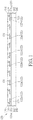
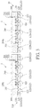
- FIG. 1 to FIG. 5 illustrate an exemplary method for fabricating a semiconductor package according to one embodiment of the invention.
- a carrier substrate 100 is provided.
- the carrier substrate 100 may comprise glass, silicon, ceramic, metal, but is not limited thereto.
- a release layer 102 may be formed on a top surface of the carrier substrate 100.
- a redistribution layer (RDL) structure 120 is then formed on the release layer 102.
- the RDL structure 120 may comprise at least a dielectric layer 125, a first metal layer 121, a second metal layer 122, and vias 123 electrically connecting the first metal layer 121 and the second metal layer 122.
- the first metal layer 121 may comprise conductive element pads 121a and the second metal layer 122 may comprise bump pads 122a, metal trace 122b, and pads 122c. It is understood that the layers and patterns in the RDL structure 120 as depicted in the figures are for illustration purposes only. The number of the metal layers in the RDL structure 120 may depend upon the design requirements.
- the first metal layer 121 and the second metal layer 122 may comprise aluminum, copper, tungsten, titanium, titanium nitride, or the like.
- the dielectric layer 125 may comprise any suitable insulating materials including, but not limited to, photo image dielectric (PID) materials, prepreg, resin materials such as Ajinomoto Build-up Film (ABF) or the like.
- the metal patterns in the dielectric layer 125 may be formed by build-up processes and plating processes, but is not limited thereto.
- the dielectric layer 125 may comprise inorganic materials such as silicon oxide, silicon nitride or the like, and the metal patterns in the dielectric layer 125 may be formed by photolithographic processes and etching processes.
- the metal traces or metal patterns formed in the dielectric layer 125 may have a line width ranging between 1 ⁇ 10 micrometers and a space (between two adjacent lines) ranging between 1 ⁇ 10 micrometers, but is not limited thereto.
- a solder mask 130 may be formed on the dielectric layer 125 and the second metal layer 122.
- the solder mask 130 may comprise a plurality of openings 131 that expose the bump pads 122a of the second metal layer 122, respectively.
- an organic solderability preservatives (OSP) film (not shown) may be applied onto the exposed surfaces of the bump pads 122a.
- each of the semiconductor dice 200 is a flip-chip with its active surface 200a facing down toward the RDL structure 120.
- a plurality of input/output (I/O) pads 201 may be disposed on the active surface 200a of each of the semiconductor dice 200.
- a connecting element 202 such as a metal bump or a metal pillar may be disposed on each of the I/O pads 201.
- the connecting element 202 is connected to a corresponding bump pad 122a through, for example, solder 203.
- a passive device 210 such as a decoupling capacitor, a resistor, or an inductor may be mounted onto the RDL structure 120.
- the passive device 210 may be mounted on the pads 122c by using surface mount technique (SMT).
- the carrier substrate 100 and the release layer 102 are removed to thereby expose a lower surface of the RDL structure 120.
- the de-bonding of the carrier substrate 100 may be performed by using heating, laser, UV/IR irradiation, or mechanical peeling, but not limited thereto.
- the conductive element pads 121a of the first metal layer 121 are revealed.
- conductive structures 410 are disposed on respective conductive element pads 121a of the first metal layer 121 to complete a semiconductor 10.
- the semiconductor 10 is then subjected to a wafer dicing process and singulated into individual die packages 1.
- the conductive structures 410 could be solder balls, solder bumps, copper pillar bumps, or any combination thereof, but is not limited thereto.
- FIG. 5 is a schematic, cross-sectional diagram illustrating a package-on-package (PoP).
- TMVs through mold vias
- the TMVs 320 may be formed through the entire thickness of the molding compound 300 for further connection.
- the TMVs 320 may be formed by drilling through holes into the molding compound 300, then filling the through holes with metal such as copper.
- the TMVs 320 may be formed prior to the wafer dicing process, but is not limited thereto.
- the die package 1 functions as a lower package
- an upper package 2 is mounted directly on the die package 1.
- the upper package 2 may be a DRAM chip package, but is not limited thereto.
- the upper package 2 may comprise a chip (such as a DRAM chip, not shown), which may be electrically connected to the lower package through the TMVs 320 and the RDL structure 120.
- the upper package 2 may comprise a plurality of connecting elements 21 such as conductive structures or bumps, which is used to connect the upper package 2 with the TMVs 320.
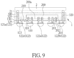
- FIG. 6 to FIG. 9 illustrate another method for fabricating TMVs and a PoP according to another embodiment of the invention, wherein like numeral numbers designate like elements, layers, or regions.
- a carrier substrate 100 is provided.
- the carrier substrate 100 may comprise glass, silicon, ceramic, metal, but is not limited thereto.
- a release layer 102 may be formed on a top surface of the carrier substrate 100.
- An RDL structure 120 is then formed on the release layer 102.
- the RDL structure 120 may comprise at least a dielectric layer 125, a first metal layer 121, a second metal layer 122, and vias 123 electrically connecting the first metal layer 121 and the second metal layer 122.
- the first metal layer 121 may comprise conductive element pads 121a and the second metal layer 122 may comprise bump pads 122a, metal trace 122b, pads 122c, and pads 122d.
- solder mask 130 may be formed on the dielectric layer 125 and the second metal layer 122.
- the solder mask 130 may comprise a plurality of openings 131 that expose the bump pads 122a of the second metal layer 122, respectively.
- a plurality of metal pillars 320a is formed on the pads 122d at a peripheral region on the RDL structure 120.
- a photoresist layer (not shown) is formed on the RDL structure 120.
- a photolithographic process is then performed to form via openings in the photoresist layer.
- the via openings are aligned with the pads 122d.
- metal such as copper may be deposited into the via openings by chemical vapor deposition (CVD), physical vapor deposition (PVD), atomic layer deposition (ALD), or plating process.
- CVD chemical vapor deposition
- PVD physical vapor deposition
- ALD atomic layer deposition
- each of the semiconductor dice 200 is a flip-chip or die with its active surface 200a facing down toward the RDL structure 120.
- a plurality of input/output (I/O) pads 201 may be disposed on the active surface 200a of each of the semiconductor dice 200.
- a connecting element 202 such as a metal bump or a metal pillar may be disposed on each of the I/O pads 201.
- the connecting element 202 is connected to a corresponding bump pad 122a through, for example, solder 203.
- a passive device 210 such as a decoupling capacitor, a resistor, or an inductor may be mounted onto the RDL structure 120.
- the passive device 210 may be mounted on the pads 122c by using surface mount technique (SMT).
- a molding compound 300 is applied.
- the molding compound 300 at least covers the semiconductor dice 200, the passive device 210, the metal pillars 320a, and the top surface of the RDL structure 120, thereby forming a wafer-level package 10.
- CMP chemical mechanical polishing
- TSVs through mold vias
- the carrier substrate 100 and the release layer 102 are removed to thereby expose a lower surface of the RDL structure 120.
- the de-bonding of the carrier substrate 100 may be performed by using heating, laser, UV/IR irradiation, or mechanical peeling, but not limited thereto.
- the conductive element pads 121a of the first metal layer 121 are revealed.
- conductive structures 410 are disposed on respective conductive element pads 121a of the first metal layer 121 to complete a semiconductor 10.
- the semiconductor 10 is then subjected to a wafer dicing process and singulated into individual die packages 1.
- an upper package 2 is mounted on the die package 1.
- the upper package 2 may be a DRAM chip package, but is not limited thereto.
- the upper package 2 may comprise a chip (such as a DRAM chip, not shown), which may be electrically connected to the lower package through the TMVs 320 and the RDL structure 120.
- the upper package 2 may comprise a plurality of connecting elements 21 such as conductive structures or bumps, which is used to connect the upper package 2 with the TMVs 320.
Landscapes
- Production Of Multi-Layered Print Wiring Board (AREA)
- Structures Or Materials For Encapsulating Or Coating Semiconductor Devices Or Solid State Devices (AREA)
- Encapsulation Of And Coatings For Semiconductor Or Solid State Devices (AREA)
Abstract
Description
- This disclosure relates generally to the field of semiconductor packaging. More particular, this disclosure relates to a fan-out semiconductor package with a redistribution layer (RDL), a package-on-package, and methods for fabricating the same.
- Fan-out wafer level packaging (FOWLP) is an embedded type packaging method during wafer level processing and is also a major advanced packaging technology for packaging a large quantity of inputs and outputs (I/O) with high integration flexibility.
- Typically, in a fan-out wafer level packaging process, semiconductor dice are placed face down on a temporary tape carrier. The semiconductor dice and temporary tape carrier are overmolded with a molding compound. After molding, the tape carrier is removed, leaving the active surfaces of the semiconductor dice exposed in a structure commonly referred to as a reconstituted wafer.
- Subsequently, a redistribution layer (RDL) structure is formed on top of the reconstituted wafer. Ball grid array (BGA) balls are attached onto the RDL structure and then the reconstituted wafer is singulated to form individual packages.
- One object of the present disclosure is to provide an improved semiconductor package and a method for fabricating the semiconductor package.
- This is achieved by a semiconductor package according to the pre-characterizing clause of
claim 1. The dependent claims pertain to corresponding further developments and improvements. - As will be seen more clearly from the detailed description following below, the includes a redistribution layer (RDL) structure having opposite first and second surfaces. The RDL structure comprises at least a bump pad on the first surface. A semiconductor die is mounted on the first surface of the RDL structure. The semiconductor die is a flip-chip with its active surface facing toward the RDL structure. A plurality of input/output (I/O) pads is disposed on the active surface of the semiconductor die. A connecting element is disposed on each of the I/O pads. The connecting element is connected to the bump pad through solder. A molding compound encapsulates the semiconductor die and covers the first surface of the RDL structure. A plurality of conductive structure is mounted on the second surface of the RDL structure.
- According to another aspect of the disclosure, a method for fabricating a semiconductor package is disclosed. A carrier substrate is provided. A redistribution layer (RDL) structure is formed on the carrier substrate. The RDL structure comprises at least a bump pad. A semiconductor die is mounted on the RDL structure. A molding compound is formed on the semiconductor die and the RDL structure. The carrier substrate is removed to reveal a plurality of solder ball pads of the RDL structure. A plurality of conductive structures is formed on the solder ball pads.
- According to still another aspect of the disclosure, a package-on-package (PoP) is disclosed. The PoP includes a lower package and an upper package mounted on the lower package. The lower package includes a redistribution layer (RDL) structure having opposite first and second surfaces. The RDL structure comprises at least a bump pad on the first surface. A semiconductor die is mounted on the first surface of the RDL structure. The semiconductor die is a flip-chip with its active surface facing toward the RDL structure. A plurality of input/output (I/O) pads is disposed on the active surface of the semiconductor die. A connecting element is disposed on each of the I/O pads. The connecting element is connected to the bump pad. A molding compound encapsulates the semiconductor die and covers the first surface of the RDL structure. Through mold vias (TMVs) are formed in the molding compound. A plurality of conductive elements are mounted on the second surface of the RDL structure. The upper package is electrically connected to the lower package through the TMVs.
- These and other objectives of the present invention will no doubt become obvious to those of ordinary skill in the art after reading the following detailed description of the preferred embodiment that is illustrated in the various figures and drawings.
- The accompanying drawings are included to provide a further understanding of the embodiments, and are incorporated in and constitute a part of this specification. The drawings illustrate some of the embodiments and, together with the description, serve to explain their principles. In the drawings:
-
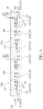
FIG. 1 to FIG. 5 illustrate an exemplary method for fabricating a semiconductor package according to the invention, whereinFIG. 4 shows a semiconductor package with an underfill between the semiconductor die and the RDL structure, andFIG. 5 illustrates a package-on-package (PoP); and -
FIG. 6 to FIG. 9 illustrate an exemplary method for fabricating through mold vias (TMVs) and a PoP according to another embodiment of the invention. - In the following detailed description of the disclosure, reference is made to the accompanying drawings, which form a part hereof, and in which is shown, by way of illustration, specific embodiments in which the invention may be practiced. These embodiments are described in sufficient detail to enable those skilled in the art to practice the invention. Other embodiments may be utilized and structural changes may be made without departing from the scope of the present disclosure.
- The following detailed description is, therefore, not to be taken in a limiting sense, and the scope of the present invention is defined only by the appended claims, along with the full scope of equivalents to which such claims are entitled.
- One or more implementations of the present invention will now be described with reference to the attached drawings, wherein like reference numerals are used to refer to like elements throughout, and wherein the illustrated structures are not necessarily drawn to scale. The terms "die", "chip", "semiconductor chip", and "semiconductor die" are used interchangeable throughout the specification.
-
FIG. 1 to FIG. 5 illustrate an exemplary method for fabricating a semiconductor package according to one embodiment of the invention. - As shown in
FIG. 1 , acarrier substrate 100 is provided. According to one embodiment, thecarrier substrate 100 may comprise glass, silicon, ceramic, metal, but is not limited thereto. According to one embodiment, arelease layer 102 may be formed on a top surface of thecarrier substrate 100. - A redistribution layer (RDL)
structure 120 is then formed on therelease layer 102. TheRDL structure 120 may comprise at least adielectric layer 125, afirst metal layer 121, asecond metal layer 122, andvias 123 electrically connecting thefirst metal layer 121 and thesecond metal layer 122. - According to one embodiment, for example, the
first metal layer 121 may compriseconductive element pads 121a and thesecond metal layer 122 may comprisebump pads 122a,metal trace 122b, andpads 122c. It is understood that the layers and patterns in theRDL structure 120 as depicted in the figures are for illustration purposes only. The number of the metal layers in theRDL structure 120 may depend upon the design requirements. - According to one embodiment, the
first metal layer 121 and thesecond metal layer 122 may comprise aluminum, copper, tungsten, titanium, titanium nitride, or the like. Thedielectric layer 125 may comprise any suitable insulating materials including, but not limited to, photo image dielectric (PID) materials, prepreg, resin materials such as Ajinomoto Build-up Film (ABF) or the like. - According to one embodiment, the metal patterns in the
dielectric layer 125 may be formed by build-up processes and plating processes, but is not limited thereto. In another embodiment, thedielectric layer 125 may comprise inorganic materials such as silicon oxide, silicon nitride or the like, and the metal patterns in thedielectric layer 125 may be formed by photolithographic processes and etching processes. - According to one embodiment, the metal traces or metal patterns formed in the
dielectric layer 125 may have a line width ranging between 1∼10 micrometers and a space (between two adjacent lines) ranging between 1∼10 micrometers, but is not limited thereto. - According to one embodiment, optionally, after the formation of the
RDL structure 120, asolder mask 130 may be formed on thedielectric layer 125 and thesecond metal layer 122. Thesolder mask 130 may comprise a plurality ofopenings 131 that expose thebump pads 122a of thesecond metal layer 122, respectively. Optionally, an organic solderability preservatives (OSP) film (not shown) may be applied onto the exposed surfaces of thebump pads 122a. - As shown in
FIG. 2 , after the formation of theRDL structure 120,semiconductor dice 200 are mounted within chip mounting areas on theRDL structure 120. According to one embodiment, each of thesemiconductor dice 200 is a flip-chip with itsactive surface 200a facing down toward theRDL structure 120. A plurality of input/output (I/O)pads 201 may be disposed on theactive surface 200a of each of thesemiconductor dice 200. A connectingelement 202 such as a metal bump or a metal pillar may be disposed on each of the I/O pads 201. The connectingelement 202 is connected to acorresponding bump pad 122a through, for example,solder 203. - Optionally, a
passive device 210 such as a decoupling capacitor, a resistor, or an inductor may be mounted onto theRDL structure 120. For example, thepassive device 210 may be mounted on thepads 122c by using surface mount technique (SMT). - As shown in
FIG. 3 , after mounting thesemiconductor dice 200 on theRDL structure 120, amolding compound 300 is applied. Themolding compound 300 at least covers thesemiconductor dice 200, thepassive device 210, and the top surface of theRDL structure 120, thereby forming a wafer-level package 10. According to one embodiment, themolding compound 300 may be subjected to a curing process. Themolding compound 300 may comprise a mixture of epoxy and silica fillers, but not limited thereto. - According to another embodiment, as shown in
FIG. 4 , prior to the formation of themolding compound 300, anunderfill 310 may be applied between each of thesemiconductor dice 200 and theRDL structure 120. Theunderfill 310 may be a silica filled epoxy, but is not limited thereto. Theunderfill 310 fills the gap (or standoff) between each of thesemiconductor dice 200 and theRDL structure 120. - Subsequently, the
carrier substrate 100 and therelease layer 102 are removed to thereby expose a lower surface of theRDL structure 120. The de-bonding of thecarrier substrate 100 may be performed by using heating, laser, UV/IR irradiation, or mechanical peeling, but not limited thereto. After thecarrier substrate 100 is removed, theconductive element pads 121a of thefirst metal layer 121 are revealed. - According to one embodiment, no metal finish is formed on the
conductive element pads 121a of thefirst metal layer 121. The thickness of thefirst metal layer 121 may range between 1 and 20 micrometers. According to another embodiment, a metal finish such as Ni, Au, and/or other elemental metals may be formed on theconductive element pads 121a of thefirst metal layer 121. - Subsequently,
conductive structures 410 are disposed on respectiveconductive element pads 121a of thefirst metal layer 121 to complete asemiconductor 10. Thesemiconductor 10 is then subjected to a wafer dicing process and singulated into individual die packages 1. According to one embodiment, theconductive structures 410 could be solder balls, solder bumps, copper pillar bumps, or any combination thereof, but is not limited thereto. -
FIG. 5 is a schematic, cross-sectional diagram illustrating a package-on-package (PoP). As shown inFIG. 5 , through mold vias (TMVs) 320 may be formed through the entire thickness of themolding compound 300 for further connection. According to one embodiment, theTMVs 320 may be formed by drilling through holes into themolding compound 300, then filling the through holes with metal such as copper. TheTMVs 320 may be formed prior to the wafer dicing process, but is not limited thereto. - In the illustrated PoP configuration, the
die package 1 functions as a lower package, anupper package 2 is mounted directly on thedie package 1. For example, theupper package 2 may be a DRAM chip package, but is not limited thereto. Theupper package 2 may comprise a chip (such as a DRAM chip, not shown), which may be electrically connected to the lower package through theTMVs 320 and theRDL structure 120. Theupper package 2 may comprise a plurality of connectingelements 21 such as conductive structures or bumps, which is used to connect theupper package 2 with theTMVs 320. -
FIG. 6 to FIG. 9 illustrate another method for fabricating TMVs and a PoP according to another embodiment of the invention, wherein like numeral numbers designate like elements, layers, or regions. - As shown in
FIG. 6 , likewise, acarrier substrate 100 is provided. Thecarrier substrate 100 may comprise glass, silicon, ceramic, metal, but is not limited thereto. Arelease layer 102 may be formed on a top surface of thecarrier substrate 100. AnRDL structure 120 is then formed on therelease layer 102. - The
RDL structure 120 may comprise at least adielectric layer 125, afirst metal layer 121, asecond metal layer 122, and vias 123 electrically connecting thefirst metal layer 121 and thesecond metal layer 122. Thefirst metal layer 121 may compriseconductive element pads 121a and thesecond metal layer 122 may comprisebump pads 122a,metal trace 122b,pads 122c, and pads 122d. - After the formation of the
RDL structure 120, asolder mask 130 may be formed on thedielectric layer 125 and thesecond metal layer 122. Thesolder mask 130 may comprise a plurality ofopenings 131 that expose thebump pads 122a of thesecond metal layer 122, respectively. - Subsequently, a plurality of
metal pillars 320a is formed on the pads 122d at a peripheral region on theRDL structure 120. For example, to form themetal pillars 320a, a photoresist layer (not shown) is formed on theRDL structure 120. A photolithographic process is then performed to form via openings in the photoresist layer. The via openings are aligned with the pads 122d. Subsequently, metal such as copper may be deposited into the via openings by chemical vapor deposition (CVD), physical vapor deposition (PVD), atomic layer deposition (ALD), or plating process. The photoresist layer is then removed. - As shown in
FIG. 7 , after the formation of themetal pillars 320a,semiconductor dice 200 are mounted within chip mounting areas on theRDL structure 120. According to one embodiment, each of thesemiconductor dice 200 is a flip-chip or die with itsactive surface 200a facing down toward theRDL structure 120. A plurality of input/output (I/O)pads 201 may be disposed on theactive surface 200a of each of thesemiconductor dice 200. A connectingelement 202 such as a metal bump or a metal pillar may be disposed on each of the I/O pads 201. The connectingelement 202 is connected to acorresponding bump pad 122a through, for example,solder 203. - Optionally, a
passive device 210 such as a decoupling capacitor, a resistor, or an inductor may be mounted onto theRDL structure 120. For example, thepassive device 210 may be mounted on thepads 122c by using surface mount technique (SMT). - As shown in
FIG. 8 , after mounting thesemiconductor dice 200 on theRDL structure 120, amolding compound 300 is applied. Themolding compound 300 at least covers thesemiconductor dice 200, thepassive device 210, themetal pillars 320a, and the top surface of theRDL structure 120, thereby forming a wafer-level package 10. Optionally, a chemical mechanical polishing (CMP) process may be performed to reveal the top surfaces of themetal pillars 320a, thereby forming through mold vias (TMVs) 320. - Subsequently, the
carrier substrate 100 and therelease layer 102 are removed to thereby expose a lower surface of theRDL structure 120. The de-bonding of thecarrier substrate 100 may be performed by using heating, laser, UV/IR irradiation, or mechanical peeling, but not limited thereto. After thecarrier substrate 100 is removed, theconductive element pads 121a of thefirst metal layer 121 are revealed. - Subsequently,
conductive structures 410 are disposed on respectiveconductive element pads 121a of thefirst metal layer 121 to complete asemiconductor 10. Thesemiconductor 10 is then subjected to a wafer dicing process and singulated into individual die packages 1. - As shown in
FIG. 9 , anupper package 2 is mounted on thedie package 1. For example, theupper package 2 may be a DRAM chip package, but is not limited thereto. Theupper package 2 may comprise a chip (such as a DRAM chip, not shown), which may be electrically connected to the lower package through theTMVs 320 and theRDL structure 120. Theupper package 2 may comprise a plurality of connectingelements 21 such as conductive structures or bumps, which is used to connect theupper package 2 with theTMVs 320.
Claims (8)
- A semiconductor package, comprising:a redistribution layer (RDL) structure having opposite first and second surfaces, wherein the RDL structure comprises at least a bump pad on the first surface;a semiconductor die mounted on the first surface of the RDL structure, wherein the semiconductor die is a flip-chip with its active surface facing toward the RDL structure, wherein a plurality of input/output (I/O) pads is disposed on the active surface of the semiconductor die, and wherein a connecting element is disposed on each of the I/O pads, and wherein the connecting element is connected to the bump pad;a molding compound encapsulating the semiconductor die and covering the first surface of the RDL structure; anda plurality of conductive structure mounted on the second surface of the RDL structure.
- The semiconductor package according to claim 1, characterised in that the RDL structure comprises at least a dielectric layer, a first metal layer on the first surface, a second metal layer on the second surface, and a via layer electrically connecting the first metal layer and the second metal layer.
- The semiconductor package according to claim 1, characterised in that the connecting element comprises a metal bump or a metal pillar.
- The semiconductor package according to claim 1, characterised in that the connecting element is connected to the bump pad through a solder.
- The semiconductor package according to claim 1 further comprising a passive device mounted on the first surface of the RDL structure.
- The semiconductor package according to claim 5, characterised in that the passive device comprises a decoupling capacitor, a resistor, or an inductor.
- The semiconductor package according to claim 1 further comprising an underfill disposed between the semiconductor die and the RDL structure.
- A package-on-package, comprising:a lower semiconductor package according to claim 1; andan upper semiconductor package on the lower semiconductor package, wherein the upper semiconductor package is electrically connected to the lower semiconductor package through the TMVs.
Applications Claiming Priority (2)
| Application Number | Priority Date | Filing Date | Title |
|---|---|---|---|
| US201662393254P | 2016-09-12 | 2016-09-12 | |
| US15/638,388 US10217716B2 (en) | 2016-09-12 | 2017-06-30 | Semiconductor package and method for fabricating the same |
Publications (1)
| Publication Number | Publication Date |
|---|---|
| EP3293759A1 true EP3293759A1 (en) | 2018-03-14 |
Family
ID=59350669
Family Applications (1)
| Application Number | Title | Priority Date | Filing Date |
|---|---|---|---|
| EP17180882.7A Withdrawn EP3293759A1 (en) | 2016-09-12 | 2017-07-12 | Semiconductor package and method for fabricating the same |
Country Status (4)
| Country | Link |
|---|---|
| US (1) | US10217716B2 (en) |
| EP (1) | EP3293759A1 (en) |
| CN (1) | CN107818956A (en) |
| TW (1) | TW201826409A (en) |
Families Citing this family (28)
| Publication number | Priority date | Publication date | Assignee | Title |
|---|---|---|---|---|
| US9515017B2 (en) * | 2014-12-18 | 2016-12-06 | Intel Corporation | Ground via clustering for crosstalk mitigation |
| KR20170053416A (en) * | 2015-11-06 | 2017-05-16 | 주식회사 엘지화학 | Semiconductor device and manufacturing method of the same |
| US10211071B2 (en) * | 2016-01-29 | 2019-02-19 | Nxp B.V. | IC packaging method and a packaged IC device |
| CN106601627A (en) * | 2016-12-21 | 2017-04-26 | 江苏长电科技股份有限公司 | Process of first sealing then corrosion electro copper column conduction three-dimensional packaging structure |
| TWI666743B (en) * | 2017-09-29 | 2019-07-21 | Phoenix & Corporation | Sensor package and method of manufacturing the same |
| CN112166502B (en) * | 2018-05-31 | 2023-01-13 | 华为技术有限公司 | Flip chip packaging structure and electronic equipment |
| KR102536269B1 (en) * | 2018-09-14 | 2023-05-25 | 삼성전자주식회사 | semiconductor package and method for manufacturing the same |
| JP7207927B2 (en) * | 2018-09-28 | 2023-01-18 | 株式会社ディスコ | Semiconductor package manufacturing method |
| TWI671873B (en) * | 2018-10-30 | 2019-09-11 | 力成科技股份有限公司 | Semiconductor package structure |
| US10903561B2 (en) * | 2019-04-18 | 2021-01-26 | Advanced Semiconductor Engineering, Inc. | Semiconductor device package and method of manufacturing the same |
| KR102494920B1 (en) * | 2019-05-21 | 2023-02-02 | 삼성전자주식회사 | Semiconductor package |
| CN110349861A (en) * | 2019-06-27 | 2019-10-18 | 深圳第三代半导体研究院 | A kind of novel PoP encapsulating structure and preparation method thereof |
| KR102551352B1 (en) | 2019-06-28 | 2023-07-04 | 삼성전자 주식회사 | Semiconductor package and method of manufacturing the same |
| KR102905973B1 (en) | 2019-07-22 | 2025-12-29 | 삼성전자 주식회사 | Semiconductor package |
| US11862587B2 (en) | 2019-07-25 | 2024-01-02 | Advanced Semiconductor Engineering, Inc. | Semiconductor package structure and method of manufacturing the same |
| CN111106013B (en) * | 2019-10-31 | 2022-03-15 | 广东芯华微电子技术有限公司 | Preparation method of TMV structure, large-board fan-out heterogeneous integrated packaging structure and preparation method thereof |
| KR102863078B1 (en) | 2020-03-27 | 2025-09-19 | 삼성전자주식회사 | Semiconductor package |
| US20210366852A1 (en) * | 2020-05-25 | 2021-11-25 | Nanya Technology Corporation | Semiconductor structure and method of forming the same |
| US11430776B2 (en) * | 2020-06-15 | 2022-08-30 | Taiwan Semiconductor Manufacturing Co., Ltd. | Semiconductor devices and methods of manufacturing |
| CN111883437B (en) * | 2020-07-03 | 2023-04-25 | 矽磐微电子(重庆)有限公司 | Semiconductor packaging method and semiconductor packaging structure |
| KR102883707B1 (en) * | 2020-07-10 | 2025-11-10 | 삼성전자주식회사 | Semiconductor package and method for manufacturing semiconductor package |
| CN115579295A (en) * | 2021-06-21 | 2023-01-06 | 讯芯电子科技(中山)有限公司 | Method for manufacturing semiconductor packaging structure |
| CN114334852B (en) * | 2021-12-29 | 2025-07-22 | 苏州汉天下电子有限公司 | Package structure of semiconductor device |
| US20230317693A1 (en) * | 2022-03-29 | 2023-10-05 | nD-HI Technologies Lab, Inc. | Die package, ic package and manufacturing process thereof |
| KR20240014949A (en) * | 2022-07-26 | 2024-02-02 | 삼성전자주식회사 | Method of manufacturing semiconductor package |
| CN115050654B (en) * | 2022-08-17 | 2022-11-08 | 甬矽电子(宁波)股份有限公司 | Preparation method of fan-in type packaging structure and fan-in type packaging structure |
| CN117737653B (en) * | 2023-12-19 | 2024-08-16 | 深圳市知音科技有限公司 | Strippable copper carrier plate, preparation method thereof and application thereof in advanced packaging |
| CN118073332B (en) * | 2024-02-26 | 2025-10-28 | 广州增芯科技有限公司 | A flip chip structure, semiconductor device and preparation method |
Citations (7)
| Publication number | Priority date | Publication date | Assignee | Title |
|---|---|---|---|---|
| US20090008762A1 (en) * | 2007-07-02 | 2009-01-08 | Nepes Corporation | Ultra slim semiconductor package and method of fabricating the same |
| US20130175694A1 (en) * | 2012-01-06 | 2013-07-11 | Taiwan Semiconductor Manufacturing Company, Ltd. | Packages and Method of Forming the Same |
| US20140185264A1 (en) * | 2012-12-28 | 2014-07-03 | Taiwan Semiconductor Manufacturing Company, Ltd. | Methods and apparatus for forming package-on-packages |
| US20140264933A1 (en) * | 2013-03-15 | 2014-09-18 | Taiwan Semiconductor Manufacturing Company, Ltd. | Wafer Level Chip Scale Packaging Intermediate Structure Apparatus and Method |
| US20150137384A1 (en) * | 2013-11-19 | 2015-05-21 | Amkor Technology, Inc. | Semicondutor device with through-silicon via-less deep wells |
| US20160014898A1 (en) * | 2014-07-14 | 2016-01-14 | Ibiden Co., Ltd. | Printed wiring board |
| US20160056127A1 (en) * | 2014-08-21 | 2016-02-25 | Daeho Lee | Semiconductor package |
Family Cites Families (1)
| Publication number | Priority date | Publication date | Assignee | Title |
|---|---|---|---|---|
| US9721922B2 (en) * | 2013-12-23 | 2017-08-01 | STATS ChipPAC, Pte. Ltd. | Semiconductor device and method of forming fine pitch RDL over semiconductor die in fan-out package |
-
2017
- 2017-06-30 US US15/638,388 patent/US10217716B2/en active Active
- 2017-07-12 EP EP17180882.7A patent/EP3293759A1/en not_active Withdrawn
- 2017-09-07 CN CN201710800845.2A patent/CN107818956A/en not_active Withdrawn
- 2017-09-11 TW TW106130964A patent/TW201826409A/en unknown
Patent Citations (7)
| Publication number | Priority date | Publication date | Assignee | Title |
|---|---|---|---|---|
| US20090008762A1 (en) * | 2007-07-02 | 2009-01-08 | Nepes Corporation | Ultra slim semiconductor package and method of fabricating the same |
| US20130175694A1 (en) * | 2012-01-06 | 2013-07-11 | Taiwan Semiconductor Manufacturing Company, Ltd. | Packages and Method of Forming the Same |
| US20140185264A1 (en) * | 2012-12-28 | 2014-07-03 | Taiwan Semiconductor Manufacturing Company, Ltd. | Methods and apparatus for forming package-on-packages |
| US20140264933A1 (en) * | 2013-03-15 | 2014-09-18 | Taiwan Semiconductor Manufacturing Company, Ltd. | Wafer Level Chip Scale Packaging Intermediate Structure Apparatus and Method |
| US20150137384A1 (en) * | 2013-11-19 | 2015-05-21 | Amkor Technology, Inc. | Semicondutor device with through-silicon via-less deep wells |
| US20160014898A1 (en) * | 2014-07-14 | 2016-01-14 | Ibiden Co., Ltd. | Printed wiring board |
| US20160056127A1 (en) * | 2014-08-21 | 2016-02-25 | Daeho Lee | Semiconductor package |
Also Published As
| Publication number | Publication date |
|---|---|
| US20180076166A1 (en) | 2018-03-15 |
| US10217716B2 (en) | 2019-02-26 |
| TW201826409A (en) | 2018-07-16 |
| CN107818956A (en) | 2018-03-20 |
Similar Documents
| Publication | Publication Date | Title |
|---|---|---|
| US10217716B2 (en) | Semiconductor package and method for fabricating the same | |
| US12327812B2 (en) | Semiconductor device and manufacturing method thereof | |
| US11710693B2 (en) | Wafer level package utilizing molded interposer | |
| US11018088B2 (en) | Dummy features in redistribution layers (RDLS) and methods of forming same | |
| US9437583B1 (en) | Package-on-package assembly and method for manufacturing the same | |
| US9905551B2 (en) | Method of manufacturing wafer level packaging including through encapsulation vias | |
| KR101730691B1 (en) | Mechanisms for forming package structure | |
| US9449953B1 (en) | Package-on-package assembly and method for manufacturing the same | |
| KR101497808B1 (en) | Molding compound structure | |
| US9502360B2 (en) | Stress compensation layer for 3D packaging | |
| US20180151477A1 (en) | Chip package structure and method for forming the same | |
| CN105789062B (en) | Package structure and method of forming the same | |
| KR102459551B1 (en) | Cowos structures and methods forming same | |
| US20160358865A1 (en) | Wafer level package and fabrication method thereof | |
| TW201828375A (en) | Semiconductor device and method of manufacturing same | |
| US20170213801A1 (en) | Method for manufacturing a package-on-package assembly | |
| TWI731888B (en) | Method for fabricating stacked semicondcutor device | |
| US20180053665A1 (en) | Pre-bumped redistribution layer structure and semiconductor package incorporating such pre-bumped redistribution layer structure |
Legal Events
| Date | Code | Title | Description |
|---|---|---|---|
| PUAI | Public reference made under article 153(3) epc to a published international application that has entered the european phase |
Free format text: ORIGINAL CODE: 0009012 |
|
| AK | Designated contracting states |
Kind code of ref document: A1 Designated state(s): AL AT BE BG CH CY CZ DE DK EE ES FI FR GB GR HR HU IE IS IT LI LT LU LV MC MK MT NL NO PL PT RO RS SE SI SK SM TR |
|
| AX | Request for extension of the european patent |
Extension state: BA ME |
|
| 17P | Request for examination filed |
Effective date: 20180907 |
|
| RBV | Designated contracting states (corrected) |
Designated state(s): AL AT BE BG CH CY CZ DE DK EE ES FI FR GB GR HR HU IE IS IT LI LT LU LV MC MK MT NL NO PL PT RO RS SE SI SK SM TR |
|
| 17Q | First examination report despatched |
Effective date: 20200727 |
|
| STAA | Information on the status of an ep patent application or granted ep patent |
Free format text: STATUS: THE APPLICATION HAS BEEN WITHDRAWN |
|
| 18W | Application withdrawn |
Effective date: 20201119 |