EP3291009A1 - Method for correcting target patterns - Google Patents
Method for correcting target patterns Download PDFInfo
- Publication number
- EP3291009A1 EP3291009A1 EP17186994.4A EP17186994A EP3291009A1 EP 3291009 A1 EP3291009 A1 EP 3291009A1 EP 17186994 A EP17186994 A EP 17186994A EP 3291009 A1 EP3291009 A1 EP 3291009A1
- Authority
- EP
- European Patent Office
- Prior art keywords
- fragment
- patterns
- correction
- fragments
- target patterns
- Prior art date
- Legal status (The legal status is an assumption and is not a legal conclusion. Google has not performed a legal analysis and makes no representation as to the accuracy of the status listed.)
- Withdrawn
Links
Images


Classifications
-
- G—PHYSICS
- G03—PHOTOGRAPHY; CINEMATOGRAPHY; ANALOGOUS TECHNIQUES USING WAVES OTHER THAN OPTICAL WAVES; ELECTROGRAPHY; HOLOGRAPHY
- G03F—PHOTOMECHANICAL PRODUCTION OF TEXTURED OR PATTERNED SURFACES, e.g. FOR PRINTING, FOR PROCESSING OF SEMICONDUCTOR DEVICES; MATERIALS THEREFOR; ORIGINALS THEREFOR; APPARATUS SPECIALLY ADAPTED THEREFOR
- G03F1/00—Originals for photomechanical production of textured or patterned surfaces, e.g., masks, photo-masks, reticles; Mask blanks or pellicles therefor; Containers specially adapted therefor; Preparation thereof
- G03F1/36—Masks having proximity correction features; Preparation thereof, e.g. optical proximity correction [OPC] design processes
-
- G—PHYSICS
- G03—PHOTOGRAPHY; CINEMATOGRAPHY; ANALOGOUS TECHNIQUES USING WAVES OTHER THAN OPTICAL WAVES; ELECTROGRAPHY; HOLOGRAPHY
- G03F—PHOTOMECHANICAL PRODUCTION OF TEXTURED OR PATTERNED SURFACES, e.g. FOR PRINTING, FOR PROCESSING OF SEMICONDUCTOR DEVICES; MATERIALS THEREFOR; ORIGINALS THEREFOR; APPARATUS SPECIALLY ADAPTED THEREFOR
- G03F7/00—Photomechanical, e.g. photolithographic, production of textured or patterned surfaces, e.g. printing surfaces; Materials therefor, e.g. comprising photoresists; Apparatus specially adapted therefor
- G03F7/70—Microphotolithographic exposure; Apparatus therefor
- G03F7/70425—Imaging strategies, e.g. for increasing throughput or resolution, printing product fields larger than the image field or compensating lithography- or non-lithography errors, e.g. proximity correction, mix-and-match, stitching or double patterning
- G03F7/70433—Layout for increasing efficiency or for compensating imaging errors, e.g. layout of exposure fields for reducing focus errors; Use of mask features for increasing efficiency or for compensating imaging errors
-
- G—PHYSICS
- G03—PHOTOGRAPHY; CINEMATOGRAPHY; ANALOGOUS TECHNIQUES USING WAVES OTHER THAN OPTICAL WAVES; ELECTROGRAPHY; HOLOGRAPHY
- G03F—PHOTOMECHANICAL PRODUCTION OF TEXTURED OR PATTERNED SURFACES, e.g. FOR PRINTING, FOR PROCESSING OF SEMICONDUCTOR DEVICES; MATERIALS THEREFOR; ORIGINALS THEREFOR; APPARATUS SPECIALLY ADAPTED THEREFOR
- G03F7/00—Photomechanical, e.g. photolithographic, production of textured or patterned surfaces, e.g. printing surfaces; Materials therefor, e.g. comprising photoresists; Apparatus specially adapted therefor
- G03F7/70—Microphotolithographic exposure; Apparatus therefor
- G03F7/70425—Imaging strategies, e.g. for increasing throughput or resolution, printing product fields larger than the image field or compensating lithography- or non-lithography errors, e.g. proximity correction, mix-and-match, stitching or double patterning
- G03F7/70433—Layout for increasing efficiency or for compensating imaging errors, e.g. layout of exposure fields for reducing focus errors; Use of mask features for increasing efficiency or for compensating imaging errors
- G03F7/70441—Optical proximity correction [OPC]
-
- G—PHYSICS
- G06—COMPUTING OR CALCULATING; COUNTING
- G06F—ELECTRIC DIGITAL DATA PROCESSING
- G06F17/00—Digital computing or data processing equipment or methods, specially adapted for specific functions
- G06F17/10—Complex mathematical operations
- G06F17/16—Matrix or vector computation, e.g. matrix-matrix or matrix-vector multiplication, matrix factorization
Definitions
- the present invention generally relates to the field of semiconductor manufacturing technologies and, more particularly, relates to methods for correcting target patterns and masks having corrected target patterns in photolithography processes.
- CD critical dimension
- OPE optical proximity effect
- OPC optical proximity correction
- the OPC method is able to correct the edge placement error (EPE) between the exposure patterns on a silicon wafer and the target patterns by multiple iterating steps.
- EPE edge placement error
- the OPC method is unable to correct the conflicting errors caused by the design.
- the conflicting errors refer to that correcting one error increases the error of other adjacent patterns. Such conflicting errors are unable to be solved simultaneously.
- a first aspect of the present invention provides a method for correcting target patterns.
- the method includes providing target patterns; dividing contours of target patterns into a plurality of fragments; performing an optical proximity correction on the target patterns to obtain mask patterns; performing an optical simulation on the target patterns to obtain simulated exposure patterns; detecting the simulated exposure patterns to find out existence of at least one weak point; determining a correction window in the target patterns according to the at least one weak point; comparing the target patterns in the correction window with patterns in a corresponding region of the simulated exposure patterns to obtain a position error of each fragment; calculating an effect value of a correction value of each fragment in the correction window on position errors of all fragments in the correction window; determining the correction value of each fragment according to the effect value of the correction value of each fragment in the correction window on position errors of all fragments in the correction window and the position error of each fragment; and correcting the target patterns using the correction value of each fragment to obtain corrected target patterns.
- the at least one weak point is a conflicting weak point.
- the optical proximity correction to the simulated exposure patterns at the weak point affects the plurality of patterns simultaneously.
- calculating the effect value of the correction value of each fragment in the correction window to position errors of all fragments in the correction window comprises: calculating a position disturbing matrix T of all the fragments in the correction window.
- the position disturbing matrix T of all the fragments in the correction window comprises: diagonal elements, which are position errors generated by any selected fragment when an unit-distance correction value is applied to the selected fragment of the plurality of fragments in the correction window; and off-diagonal elements, which are position errors generated by all other fragments than the selected fragment when an unit-distance correction value is applied to the selected fragment of the plurality of fragments in the correction window.
- the diagonal elements of the position disturbing matrix T are greater than the off-diagonal elements of the position disturbing matrix T.
- the number of the fragments in the correction window being "n"
- the position disturbing matrix T is an n ⁇ n order matrix
- values of the elements T ii are in a range of approximately 1 nm to 5 nm.
- values of the elements T ij are in a range of approximately 0 to 1 nm.
- determining the correction value of each fragment according to the effect value of the correction value of each fragment in the correction window to position errors of all fragments in the correction window and the position errors of all the fragments comprises: calculating an inverse matrix T -1 of the position disturbing matrix T; and calculating the correction value of each fragment according to the inverse matrix T -1 and the position error of each fragment.
- the correction value of each fragment is less than, or equal to approximately 5 nm.
- detecting the simulated exposure patterns to find out if there is at least one weak point comprises: comparing the simulated exposure patterns with the target patterns; and determining a certain location to be the weak point if the difference between the exposure patterns and the target patterns is greater than a threshold value.
- a shape of the correction window is one of rectangular and polygonal.
- an area of the correction window is in a range of approximately 200 nm ⁇ 200 nm to 500 nmx500 nm.
- the weak point is at the center of the correction window.
- the method for correcting the target patterns includes a plurality of loops; each loop includes providing target patterns, dividing contours of the target patterns into a plurality of fragments, performing an optical proximity correction to the target patterns to obtain mask patterns, performing an optical simulation on the mask patterns to obtain simulated exposure patterns, detecting the simulated exposure patterns to find out existence of at least one weak point, determining a correction window in the target patterns according to the at least one weak point, comparing the target patterns in the correction window with patterns in a corresponding region of the simulated exposure patterns to obtain a position error of each fragment, calculating an effect value of a correction value of each fragment in the correction window on position errors of all fragments in the correction window, determining the correction value of each fragment according to the effect value of the correction value of each fragment in the correction window on position errors of all fragments in the correction window and the position error of each fragment, correcting the target patterns using the correction value of each fragment to obtain corrected target patterns value of each fragment in the correction window to position errors of all fragments in the correction window and the position error of each
- the plurality of loops are ended when no weak point is found in a certain loop of the plurality of loops.
- Another aspect of the present invention includes a mask having corrected target patterns.
- the mask includes a mask substrate; and corrected target patterns formed on the mask substrate.
- the corrected targeted patterns is formed by providing target patterns; dividing contours of target patterns into a plurality of fragments; performing an optical proximity correction on the target patterns to obtain mask patterns; performing an optical simulation on the target patterns to obtain simulated exposure patterns; detecting the simulated exposure patterns to find out existence of at least one weak point; determining a correction window in the target patterns according to the at least one weak point; comparing the target patterns in the correction window with patterns in a corresponding region of the simulated exposure patterns to obtain a position error of each fragment; calculating an effect value of a correction value of each fragment in the correction window on position errors of all fragments in the correction window; determining the correction value of each fragment according to the effect value of the correction value of each fragment in the correction window on position errors of all fragments in the correction window and the position error of each fragment; and correcting the target patterns using the correction value of each fragment to obtain corrected target patterns.
- the effect value of the correction value of each fragment in the correction window to position errors of all fragments in the correction window is obtained by calculating a position disturbing matrix of all the fragments in the correction window.
- the correction value of each fragment is determined by the disturbing matrix of all the fragments and the position error of each fragment.
- a mask according to the second aspect of the present invention may be obtained by a method according to the first aspect of the present invention.
- weak points or defects which may include, for example, pinches, bridgings and/or imperfect contact holes, may exist simultaneously in a certain region of the circuits on a wafer.
- Such weak points of the photolithography process in the circuit layout may affect the properties of the finally formed circuits, or even fail the functions of the circuits.
- Figure 1 illustrates a planar structure of existing target patterns.
- the target patterns 300 include a first region 101, a second region 102 and a third region 103.
- the first region 101, the second region 102 and the third region 103 all include line regions 111 and space regions 112.
- the line regions 111 and the space regions 112 of the first region 101 and the third region 103 do not have weak points.
- the rule-based retargeting method is used to correct the line regions 111 of the second region 102, it needs to move in or move out a certain edge fragment 1111.
- a pinch defect may be generated.
- the edge fragment 1111 is moved toward the space region 112, a bridge defect may be generated.
- the optical proximity correction process of the second region 102 faces the issue that the pinch defect and the bridge defect are needed to be solved simultaneously.
- solving one error of the two errors exacerbates the other issue.
- the conflicting error caused by the two errors is difficult to solve simultaneously.
- the present invention provides a method for correcting target patterns, and a mask having corrected target patterns.
- Figure 2 illustrates a flow chart of an exemplary method for correcting target patterns consistent with the disclosed embodiments.
- the method may include providing target patterns; resolving the contours of the target patterns; and dividing the contours of the target patterns into a plurality of fragments (step S11).
- the method may include performing an optical proximity correction (OPC) process on the target patterns to obtain mask patterns (step S 13).
- OPC optical proximity correction
- the OPC process may include forming an initial mask layout using a rule-based retargeting method, then performing one or more times of the OPC process on the initial mask layout to obtain the mask patterns.
- the target patterns refer to the expected exposure patterns that match the function and manufacturing requirements of ICs.
- the method may include performing an optical simulation on the mask patterns to obtain simulated exposure patterns; and to check the existence of at least one weak point on the simulated exposure patterns.
- the process for checking the existence of at least one weak point on the simulated mask patterns may include using an OPC simulation software to perform an optical simulation process on the mask patterns to obtain the simulated exposure patterns so as to simulate the target patterns formed on a silicon wafer by a certain photolithography process (using certain parameters, such as the intensity and the wavelength of the exposure light, and the exposure focusing length, etc.) using the mask patterns; and comparing the simulated exposure patterns with the current target patterns. If their difference is greater than a certain threshold value at a certain location, such a location may be determined as a weak point.
- the region that easily has the deformation and distortion issue i.e., weak points
- the weak point may be portions of the exposure patterns that have small distances, and/or the portions of the exposure patterns at the L-shape corner regions, etc.
- the process for correcting the target patterns may be ended. That is, the mask patterns obtained in the step S13 may be the finally formed mask patterns.
- the method for correcting target patterns may also include the step S 17.
- Figure 3 illustrates a planar structure of exemplary simulated exposure patterns consistent with the disclosed embodiments.
- the simulated exposure patterns 200 illustrated in Figure 3 are for illustrative purposes only, not intended to limit the present invention.
- the weak point on the simulated exposure patterns 200 detected in the step S 13 may be referred to as the weak point 201.
- the threshold value may be pre-set; and may be determined by the critical dimension of the to-be-formed device. The threshold value may often be 3%-10% of the critical dimension of the to-be-formed device. Because the weak point 201 may be at the boundary region between the connection line 211 and the space region 212, the weak point 201 may be a conflicting weak point. That is, the weak point 201 may belong to both the pinch-type weak point and the bridge-type weak point. When the OPC method is used to correct the punch-type error, the bridge-type error may be more severe. Thus, the pinch-type error and the bridge-type error may be unable to solve simultaneously.
- the weak point 201 belonging to both the pinch-type weak point and the bridge-type weak point, is for illustrative purposes only to describe the conflicting error caused by the conflicting weak point; and is not intended to limit the present invention.
- the conflicting weak point may locate at the boundary regions of a plurality of patterns of the simulated exposure patterns.
- the OPC process to the conflicting weak point may affect the plurality of patterns; and the conflicting errors may be generated.
- the method for correcting the target patterns may also include the step S17.
- the step S 17 may include determining a correction window covering a partial number of the target patterns according to the weak point; comparing target patterns in the correction window with the patterns in the corresponding region of the simulated exposure patterns to obtain the position error of each fragment of the patterns in the correction window; and calculating the effect value of the correction value of each fragment in the correction window to the position errors of all the fragments in the correction window; determining the correction value of each fragment according to the effect value of the correction value of each fragment in the correction window to the position errors of all the fragments in the correction window and the position error of each fragment; and correcting the target patterns to obtain the corrected target patterns using the correction value of each fragment.
- Figure 4 illustrates a planar view of an exemplary correction window determined in the target patterns according to a weak point consistent with the disclosed embodiments.
- the dashed-line frame refers to the correction window 303 containing a weak point 201.
- the target patterns in the correction window 303 may include a plurality of connection lines 311; and regions between adjacent connection lines 311 may be referred to as the space regions 312.
- the contours of the connection lines 311 may be divided into a plurality of fragments 3111.
- the target patterns in the correction windows 303 may be compared with the patterns in the corresponding region of the simulated exposure patterns (not shown); and the position error of each edge (EPE) in the correction window 303 may be obtained.
- EPE position error of each edge
- the shape of the correction window 303 may be rectangle, or polygonal, etc.
- the area of the correction window 303 may be in a range of approximately 200 nmx200 nm to 500 nm ⁇ 500 nm. In one embodiment, the shape of the correction window 303 is rectangle; and the area of the correction window 303 may be approximately 400 nm ⁇ 300 nm.
- the weak point 201 may be at the center of the correction window 303.
- the shape of the correction window may be polygonal. There may be a plurality of weak points in the correction window.
- the number of the fragments of the target patterns 300 included in the correction window may be N.
- CD i (target) may refer to the position of the i th fragment in the target patterns 300; and CD i (contour) may refer to the position of the i th fragment in the simulated exposure patterns 200.
- i may be smaller than, or equal to N.
- calculating the effect value of the correction value of each fragment in the correction window 303 to the position errors of all the fragments in the correction window 303 may include calculating the position disturbing matrix of all the fragments in the correction window 303.
- the diagonal elements of the position disturbing matrix may be defined as the position error of any selected fragment generated by itself when a unit-distance correction value is applied to the selected fragment of all the fragments in the correction window 303.
- the off-diagonal elements of the position disturbing matrix may be defined the position error generated by all other fragments than the selected fragment when a unit-distance correction value is applied to the selected fragment of all the fragments in the correction window 303.
- the position disturbing matrix obtained by such a method may not only include the effect value to the position error of the selected fragment (element) itself when the selected fragment is corrected with a unit-distance, but also may include the effect value to the position error of other fragments.
- the position disturbing matrix may consider the proximity (correlation) effect among all the fragments in the region having the weak point
- the correction values determined by the position disturbing matrix may all be micro shifts.
- the resolution of the correction value may be sufficiently high. Thus, it may allow the correction of the target patterns and the subsequent OPC iterations to converge rapidly.
- such a matrix based-process may be referred as a real-time retargeting operation.
- the real-time retargeting operation may have a fast and stable convergence.
- the number of the fragments in the correction window 303 may be "n"
- the method for calculating the position disturbing matrix of all the fragments in the correction window 303 may be as following.
- the position disturbing matrix T may be an n ⁇ n order matrix.
- the elements may represent the effect value of the correction value of the j th fragment to the position error of the i th fragment. Where 1 ⁇ i, j ⁇ n; and i and j may be both positive integers.
- the diagonal elements T ii of the position disturbing matrix T may be greater than the off-diagonal elements T ij of the position disturbing matrix T.
- the value of the diagonal elements T ii of the position disturbing matrix T may be in a range of approximately 1 nm-5 nm.
- the value of the off-diagonal elements T ij of the position disturbing matrix T may be in a range of approximately 0-1 nm.
- the contours of the simulated exposure patterns may include a plurality of fragments; and the number "n" of the fragments may be dependent of the area of the selected correction window.
- the correction value of each fragment may be determined according to the position disturbing matrix and the position error of each fragment.
- the method for determining the correction value of each fragment according to the position disturbing matrix and the position error of each fragment may include calculating the inverse matrix T -1 of the position disturbing matrix T; and calculating the correction value of each fragment using the inverse matrix T -1 and the position error ⁇ Epe i of the each fragment.
- the correction value of the i th fragment may consider the effect value of the correction value of the i th fragment to the position errors of all the fragments. That is, the correction value of the i th fragment may be an effective correction value determined by considering the proximity (correlation) effect value of all the "n" fragments in the correction window.
- the correction value ⁇ f i of each fragment may not be greater than 5 nm.
- the correction value ⁇ f i of each fragment obtained by the disclosed target pattern correction method may all be relatively small shifts; and may not affect the functions of the entire target patterns.
- the target patterns may be corrected using the correction values.
- the corrected target patterns may be obtained.
- the corrected target patterns in the correction window 303 may be corrected.
- the patterns in the other regions may be kept intact; and the corrected target patterns may be obtained.
- the method for correcting the target patterns may include a plurality of loops.
- Each loop may include the step S11, the step S 13, the step S15 and the step S 17.
- the corrected target patterns in a previous loop in the plurality of loops may be used as the target patterns of a next loop.
- the step S11 may be performed, including providing target patterns; and dividing the contours of the target patterns into a plurality of fragments, etc.
- the target patterns may the target patterns obtained from the correction in the step S17.
- the weak point on the mask layout may be detected first, then the correction window may be determined according to the weak point. Then, the effect value of the correction value of each fragment to the position errors of all the fragments in the correction window may be calculated. According to the effect value of the correction value of each fragment to the position errors of all the fragments in the correction window and the position error of each fragment, the correction value of each fragment may be calculated. Then, the target patterns may be corrected using the correction value of each fragment to obtain the corrected target patterns. The corrected target patterns may be used as new target patterns to perform further OPC iterations to obtain new mask patterns. The disclosed method may perform the correction using the weak point on the target patterns, the issue that the OPC method is unable to correct the conflicting weak point on the mask patterns may be overcome. Accordingly, the conflicting errors caused by the problematic photolithography mask design may be avoided.
- the position disturbing matrix may calculate the effect value of the correction value of each fragment of the target patterns to the position errors of other fragments in the proximity regions around the weak point. That is, the proximity (correlation) effect among all the fragments around the weak point may be considered.
- the correction value of each fragment determined by the position disturbing matrix and the position error of each fragment may be have a relatively high resolution. Accordingly, the correction of the target patterns and the subsequently OPC iterations may converge rapidly and stably. On one hand, the calculation time may be significantly saved. On the other hand, the conflicting weak point caused by the problematic photolithography mask design may be eliminated.
- the corrected target patterns may be transferred to form a mask. That is, a mask may be formed; and the mask may have the corrected target patterns.
- the mask may be used in a photolithography process to form the target patterns in the photoresist layer on a wafer.
- the mask may be formed by providing a mask substrate; and forming the corrected target patterns on the mask substrate.
- the mask substrate may be a transparent substrate.
- the corrected target patterns may be formed on the mask substrate by any appropriate process, such as a direct printing process, an electron-beam lithography process, or a laser writing process, etc.
- the present invention also provides a mask for a photolithography process.
- the mask may include a mask substrate; and a plurality of corrected target patterns obtained by the disclosed target pattern correction method.
- the mask may be loaded in a photolithography apparatus; and a wafer with a photoresist layer may also be loaded in the photolithography apparatus. Then, an exposure process may performed; and target patterns may be formed in the photoresist layer.
- the disclosed mask may have no pinch-type defects and/or bridge-type defects. Thus, the quality of the target patterns formed on the wafer may be improved; and the electrical properties of the final semiconductor structures may be improved.
- the disclosed target pattern correction method may have following advantages.
- the weak point on the mask layout may be detected first, then the correction window may be determined according to the weak point. Then, the effect value of the correction value of each fragment to the position errors of all the fragments in the correction window may be calculated. According to the effect value of the correction value of each fragment to the position errors of all the fragments in the correction window and the position error of each fragment, the correction value of each fragment may be calculated. Then, the target patterns may be corrected using the correction value of each fragment to obtain the corrected target patterns. The corrected target patterns may be used as new target patterns to perform further OPC iterations to obtain new mask patterns.
- the disclosed target pattern correction method may perform the correction using the weak point on the target patterns, the issue that the OPC method is unable to correct the conflicting weak point on the mask patterns may be overcome. Accordingly, the conflicting errors caused by the problematic photolithography mask design may be avoided.
- the position disturbing matrix may calculate the effect value of the correction value of each fragment of the target patterns to the position errors of other fragments in the proximity regions around the weak point. That is, the proximity (correlation) effect among all the fragments around the weak point may be considered.
- the correction value of each fragment determined by the position disturbing matrix and the position error of each fragment may be have a relatively high resolution. Accordingly, the correction of the target patterns and the subsequently OPC iterations may converge rapidly and stably. On one hand, the calculation time may be significantly saved. On the other hand, the conflicting weak point caused by the problematic photolithography mask design may be eliminated.
- the computer system may include: at least one processing element such as a central processing unit (CPU) or a processor, and a memory. Instructions/programs may be stored on the memory such as a computer readable storage medium including, for example, a random access memory (RAM)/read-only memory (ROM), a magnetic disk, an optical disc, or the like.
- the at least one processing element may be configured to implement the disclosed methods according to the instructions/programs stored on the memory.
- the memory is a non-transitory computer readable recording medium and configured in the computer system by using the computer readable recording medium, and to perform the methods disclosed herein.
Landscapes
- Physics & Mathematics (AREA)
- General Physics & Mathematics (AREA)
- Engineering & Computer Science (AREA)
- Mathematical Physics (AREA)
- Data Mining & Analysis (AREA)
- Computational Mathematics (AREA)
- Mathematical Analysis (AREA)
- Mathematical Optimization (AREA)
- Pure & Applied Mathematics (AREA)
- Theoretical Computer Science (AREA)
- Computing Systems (AREA)
- Databases & Information Systems (AREA)
- Software Systems (AREA)
- General Engineering & Computer Science (AREA)
- Algebra (AREA)
- Preparing Plates And Mask In Photomechanical Process (AREA)
- Exposure And Positioning Against Photoresist Photosensitive Materials (AREA)
Abstract
Description
- This application claims the priority of Chinese patent application No.
201610788930.7 - The present invention generally relates to the field of semiconductor manufacturing technologies and, more particularly, relates to methods for correcting target patterns and masks having corrected target patterns in photolithography processes.
- With the continuous development of the integrated circuit (IC) manufacturing technology, the critical dimension (CD) of ICs has been continuously reduced. When the CD of ICs is reduced to a same order as the exposure wavelength of the photolithography apparatus, an optical proximity effect (OPE) occurs. Such a phenomenon is caused by the diffraction and interference of the exposure light when the exposure light passes through a mask during the photolithography process. The diffraction and interference of the exposure light cause the deformation and distortion of the structure (or contours) of patterns of the IC when the patterns are transferred from the mask to a photoresist layer on a wafer.
- To overcome the optical proximity effect, an optical proximity correction (OPC) method is often used. The OPC method pre-corrects the expected deformation and distortion of the mask patterns to cause the correction compensation value to be able to compensate the optical proximity effect generated by the exposure system of the photolithography apparatus. Accordingly, the final patterns formed on a wafer are identical to the target patterns.
- The OPC method is able to correct the edge placement error (EPE) between the exposure patterns on a silicon wafer and the target patterns by multiple iterating steps. However, the OPC method is unable to correct the conflicting errors caused by the design. The conflicting errors refer to that correcting one error increases the error of other adjacent patterns. Such conflicting errors are unable to be solved simultaneously.
- Thus, there is a need to develop a method that is able to solve the issue caused by conflicting errors.
- It is an object of the present invention to provide a method for correcting target patterns and a corresponding mask which solve the problems above and/or other problems in the art, in particular by which problems in connection caused by conflicting errors are avoided or at least reduced.
- The object is achieved by the features of the respective independent claims. Further embodiments are defined in the respective dependent claims.
- A first aspect of the present invention provides a method for correcting target patterns.
- The method includes providing target patterns; dividing contours of target patterns into a plurality of fragments; performing an optical proximity correction on the target patterns to obtain mask patterns; performing an optical simulation on the target patterns to obtain simulated exposure patterns; detecting the simulated exposure patterns to find out existence of at least one weak point; determining a correction window in the target patterns according to the at least one weak point; comparing the target patterns in the correction window with patterns in a corresponding region of the simulated exposure patterns to obtain a position error of each fragment; calculating an effect value of a correction value of each fragment in the correction window on position errors of all fragments in the correction window; determining the correction value of each fragment according to the effect value of the correction value of each fragment in the correction window on position errors of all fragments in the correction window and the position error of each fragment; and correcting the target patterns using the correction value of each fragment to obtain corrected target patterns.
- Preferably, the at least one weak point is a conflicting weak point.
- Preferably, the conflicting weak point is located at boundary regions of a plurality of patterns of the simulated exposure patterns.
- Preferably, the optical proximity correction to the simulated exposure patterns at the weak point affects the plurality of patterns simultaneously.
- Preferably, calculating the effect value of the correction value of each fragment in the correction window to position errors of all fragments in the correction window comprises: calculating a position disturbing matrix T of all the fragments in the correction window.
- Preferably, the position disturbing matrix T of all the fragments in the correction window comprises: diagonal elements, which are position errors generated by any selected fragment when an unit-distance correction value is applied to the selected fragment of the plurality of fragments in the correction window; and off-diagonal elements, which are position errors generated by all other fragments than the selected fragment when an unit-distance correction value is applied to the selected fragment of the plurality of fragments in the correction window.
- Preferably, the diagonal elements of the position disturbing matrix T are greater than the off-diagonal elements of the position disturbing matrix T.
- Preferably, the number of the fragments in the correction window being "n", wherein: the position disturbing matrix T is an n×n order matrix, and elements of the position disturbing matrix T are

- Preferably, when i=j, values of the elements Tii are in a range of approximately 1 nm to 5 nm.
- Preferably, when i≠j, values of the elements Tij are in a range of approximately 0 to 1 nm.
- Preferably, determining the correction value of each fragment according to the effect value of the correction value of each fragment in the correction window to position errors of all fragments in the correction window and the position errors of all the fragments comprises: calculating an inverse matrix T-1 of the position disturbing matrix T; and calculating the correction value of each fragment according to the inverse matrix T-1 and the position error of each fragment.
- Preferably, a correction value of an ith fragment of the n fragments is Δfi= ∑j(T-1)ijΔEpej i, j = 1, 2, ...... n, wherein: ΔEpej is a position error of a jtn fragment; and Δfi is the correction value of the ith fragment.
- Preferably, the correction value of each fragment is less than, or equal to approximately 5 nm.
- Preferably, detecting the simulated exposure patterns to find out if there is at least one weak point comprises: comparing the simulated exposure patterns with the target patterns; and determining a certain location to be the weak point if the difference between the exposure patterns and the target patterns is greater than a threshold value.
- Preferably, a shape of the correction window is one of rectangular and polygonal.
- Preferably, an area of the correction window is in a range of approximately 200 nm×200 nm to 500 nmx500 nm.
- Preferably, the weak point is at the center of the correction window.
- Preferably, the method for correcting the target patterns includes a plurality of loops; each loop includes providing target patterns, dividing contours of the target patterns into a plurality of fragments, performing an optical proximity correction to the target patterns to obtain mask patterns, performing an optical simulation on the mask patterns to obtain simulated exposure patterns, detecting the simulated exposure patterns to find out existence of at least one weak point, determining a correction window in the target patterns according to the at least one weak point, comparing the target patterns in the correction window with patterns in a corresponding region of the simulated exposure patterns to obtain a position error of each fragment, calculating an effect value of a correction value of each fragment in the correction window on position errors of all fragments in the correction window, determining the correction value of each fragment according to the effect value of the correction value of each fragment in the correction window on position errors of all fragments in the correction window and the position error of each fragment, correcting the target patterns using the correction value of each fragment to obtain corrected target patterns value of each fragment in the correction window to position errors of all fragments in the correction window and the position errors of all the fragments, and correcting the target patterns using the correction value of each fragment to obtain corrected target patterns; and the corrected target patterns obtained from a previous loop of the plurality of loops are used as target patterns of a next loop.
- Preferably, the plurality of loops are ended when no weak point is found in a certain loop of the plurality of loops.
- Another aspect of the present invention includes a mask having corrected target patterns.
- The mask includes a mask substrate; and corrected target patterns formed on the mask substrate. The corrected targeted patterns is formed by providing target patterns; dividing contours of target patterns into a plurality of fragments; performing an optical proximity correction on the target patterns to obtain mask patterns; performing an optical simulation on the target patterns to obtain simulated exposure patterns; detecting the simulated exposure patterns to find out existence of at least one weak point; determining a correction window in the target patterns according to the at least one weak point; comparing the target patterns in the correction window with patterns in a corresponding region of the simulated exposure patterns to obtain a position error of each fragment; calculating an effect value of a correction value of each fragment in the correction window on position errors of all fragments in the correction window; determining the correction value of each fragment according to the effect value of the correction value of each fragment in the correction window on position errors of all fragments in the correction window and the position error of each fragment; and correcting the target patterns using the correction value of each fragment to obtain corrected target patterns.
- Preferably, the effect value of the correction value of each fragment in the correction window to position errors of all fragments in the correction window is obtained by calculating a position disturbing matrix of all the fragments in the correction window.
- Preferably, the correction value of each fragment is determined by the disturbing matrix of all the fragments and the position error of each fragment.
- A mask according to the second aspect of the present invention may be obtained by a method according to the first aspect of the present invention.
- Other aspects of the present invention can be understood by those skilled in the art in light of the description, the claims, and the drawings of the present invention.
-
-
Figure 1 illustrates a planar structure of existing target patterns; -
Figure 2 illustrates a flow chart of an exemplary method for correcting target patterns consistent with the disclosed embodiments; -
Figure 3 illustrates a planar structure of simulated exposure patterns consistent with the disclosed embodiments; and -
Figure 4 illustrates a planar structure of an exemplary correction window determined by weak points in target patterns consistent with the disclosed embodiments. - Reference will now be made in detail to exemplary embodiments of the disclosure, which are illustrated in the accompanying drawings. Wherever possible, the same reference numbers will be used throughout the drawings to refer to the same or like parts.
- When conflicting errors occur during optical proximity correction (OPC) process for photomask design, weak points or defects, which may include, for example, pinches, bridgings and/or imperfect contact holes, may exist simultaneously in a certain region of the circuits on a wafer. Such weak points of the photolithography process in the circuit layout may affect the properties of the finally formed circuits, or even fail the functions of the circuits.
-
Figure 1 illustrates a planar structure of existing target patterns. Thetarget patterns 300 include afirst region 101, asecond region 102 and athird region 103. Thefirst region 101, thesecond region 102 and thethird region 103 all includeline regions 111 andspace regions 112. Theline regions 111 and thespace regions 112 of thefirst region 101 and thethird region 103 do not have weak points. When the rule-based retargeting method is used to correct theline regions 111 of thesecond region 102, it needs to move in or move out a certain edge fragment 1111. When the edge fragment 1111 is moved toward theline region 111, a pinch defect may be generated. When the edge fragment 1111 is moved toward thespace region 112, a bridge defect may be generated. Either the pinch defect or the bridge defect will form the process weak point on the wafer; and the properties of the final circuit may be affected. Thus, the optical proximity correction process of thesecond region 102 faces the issue that the pinch defect and the bridge defect are needed to be solved simultaneously. However, solving one error of the two errors exacerbates the other issue. The conflicting error caused by the two errors is difficult to solve simultaneously. Thus, there is a need to develop a method to solve the conflicting errors. - The present invention provides a method for correcting target patterns, and a mask having corrected target patterns.
-
Figure 2 illustrates a flow chart of an exemplary method for correcting target patterns consistent with the disclosed embodiments. - As shown in
Figure 2 , the method may include providing target patterns; resolving the contours of the target patterns; and dividing the contours of the target patterns into a plurality of fragments (step S11). - Further, the method may include performing an optical proximity correction (OPC) process on the target patterns to obtain mask patterns (step S 13).
- In some embodiments, the OPC process may include forming an initial mask layout using a rule-based retargeting method, then performing one or more times of the OPC process on the initial mask layout to obtain the mask patterns.
- In one embodiment, after forming the initial mask layout, five times of OPC iterations are used to obtain the mask patterns. The target patterns refer to the expected exposure patterns that match the function and manufacturing requirements of ICs.
- Further, the method may include performing an optical simulation on the mask patterns to obtain simulated exposure patterns; and to check the existence of at least one weak point on the simulated exposure patterns.
- In some embodiments, the process for checking the existence of at least one weak point on the simulated mask patterns may include using an OPC simulation software to perform an optical simulation process on the mask patterns to obtain the simulated exposure patterns so as to simulate the target patterns formed on a silicon wafer by a certain photolithography process (using certain parameters, such as the intensity and the wavelength of the exposure light, and the exposure focusing length, etc.) using the mask patterns; and comparing the simulated exposure patterns with the current target patterns. If their difference is greater than a certain threshold value at a certain location, such a location may be determined as a weak point.
- In some embodiments, the region that easily has the deformation and distortion issue, i.e., weak points, may be manually determined according to experience. For example, the weak point may be portions of the exposure patterns that have small distances, and/or the portions of the exposure patterns at the L-shape corner regions, etc.
- If no weak point is found in the
step S 15, the process for correcting the target patterns may be ended. That is, the mask patterns obtained in the step S13 may be the finally formed mask patterns. - If a weak point is found in the
step S 15, as shown inFigure 2 , the method for correcting target patterns may also include the step S 17. - In one embodiment, a weak point is found in the step S15.
Figure 3 illustrates a planar structure of exemplary simulated exposure patterns consistent with the disclosed embodiments. Thesimulated exposure patterns 200 illustrated inFigure 3 are for illustrative purposes only, not intended to limit the present invention. - As shown in
Figure 3 , the weak point on thesimulated exposure patterns 200 detected in the step S 13 may be referred to as theweak point 201. In one embodiment, the threshold value may be pre-set; and may be determined by the critical dimension of the to-be-formed device. The threshold value may often be 3%-10% of the critical dimension of the to-be-formed device. Because theweak point 201 may be at the boundary region between theconnection line 211 and thespace region 212, theweak point 201 may be a conflicting weak point. That is, theweak point 201 may belong to both the pinch-type weak point and the bridge-type weak point. When the OPC method is used to correct the punch-type error, the bridge-type error may be more severe. Thus, the pinch-type error and the bridge-type error may be unable to solve simultaneously. - The
weak point 201, belonging to both the pinch-type weak point and the bridge-type weak point, is for illustrative purposes only to describe the conflicting error caused by the conflicting weak point; and is not intended to limit the present invention. The conflicting weak point may locate at the boundary regions of a plurality of patterns of the simulated exposure patterns. The OPC process to the conflicting weak point may affect the plurality of patterns; and the conflicting errors may be generated. - As shown in
Figure 2 , if a weak point is found in the simulated exposure patterns in thestep S 15, the method for correcting the target patterns may also include the step S17. The step S 17 may include determining a correction window covering a partial number of the target patterns according to the weak point; comparing target patterns in the correction window with the patterns in the corresponding region of the simulated exposure patterns to obtain the position error of each fragment of the patterns in the correction window; and calculating the effect value of the correction value of each fragment in the correction window to the position errors of all the fragments in the correction window; determining the correction value of each fragment according to the effect value of the correction value of each fragment in the correction window to the position errors of all the fragments in the correction window and the position error of each fragment; and correcting the target patterns to obtain the corrected target patterns using the correction value of each fragment. -
Figure 4 illustrates a planar view of an exemplary correction window determined in the target patterns according to a weak point consistent with the disclosed embodiments. As shown inFigure 4 , the dashed-line frame refers to thecorrection window 303 containing aweak point 201. The target patterns in thecorrection window 303 may include a plurality ofconnection lines 311; and regions betweenadjacent connection lines 311 may be referred to as thespace regions 312. The contours of theconnection lines 311 may be divided into a plurality offragments 3111. The target patterns in thecorrection windows 303 may be compared with the patterns in the corresponding region of the simulated exposure patterns (not shown); and the position error of each edge (EPE) in thecorrection window 303 may be obtained. - The shape of the
correction window 303 may be rectangle, or polygonal, etc. The area of thecorrection window 303 may be in a range of approximately 200 nmx200 nm to 500 nm×500 nm. In one embodiment, the shape of thecorrection window 303 is rectangle; and the area of thecorrection window 303 may be approximately 400 nm×300 nm. Theweak point 201 may be at the center of thecorrection window 303. - In some embodiments, the shape of the correction window may be polygonal. There may be a plurality of weak points in the correction window.
- In some embodiments, the number of the fragments of the
target patterns 300 included in the correction window may be N. The position error of the ith fragment may be defined as ΔEpei = CDi (target) - (contour). CDi (target) may refer to the position of the ith fragment in thetarget patterns 300; and CDi (contour) may refer to the position of the ith fragment in thesimulated exposure patterns 200. Where i may be smaller than, or equal to N. - In some embodiments, calculating the effect value of the correction value of each fragment in the
correction window 303 to the position errors of all the fragments in thecorrection window 303 may include calculating the position disturbing matrix of all the fragments in thecorrection window 303. - Specifically, the diagonal elements of the position disturbing matrix may be defined as the position error of any selected fragment generated by itself when a unit-distance correction value is applied to the selected fragment of all the fragments in the
correction window 303. The off-diagonal elements of the position disturbing matrix may be defined the position error generated by all other fragments than the selected fragment when a unit-distance correction value is applied to the selected fragment of all the fragments in thecorrection window 303. The position disturbing matrix obtained by such a method may not only include the effect value to the position error of the selected fragment (element) itself when the selected fragment is corrected with a unit-distance, but also may include the effect value to the position error of other fragments. - Because the position disturbing matrix may consider the proximity (correlation) effect among all the fragments in the region having the weak point, the correction values determined by the position disturbing matrix may all be micro shifts. The resolution of the correction value may be sufficiently high. Thus, it may allow the correction of the target patterns and the subsequent OPC iterations to converge rapidly.
- In some embodiments, such a matrix based-process may be referred as a real-time retargeting operation. The real-time retargeting operation may have a fast and stable convergence.
- Specifically, the number of the fragments in the
correction window 303 may be "n", the method for calculating the position disturbing matrix of all the fragments in thecorrection window 303 may be as following. The position disturbing matrix T may be an n×n order matrix. The elements of the position disturbing matrix may be

- As shown in the equation (1), the diagonal elements of the position disturbing matrix T:


- In some embodiments, the diagonal elements Tii of the position disturbing matrix T may be greater than the off-diagonal elements Tij of the position disturbing matrix T.
- In some embodiments, the value of the diagonal elements Tii of the position disturbing matrix T may be in a range of approximately 1 nm-5 nm. The value of the off-diagonal elements Tij of the position disturbing matrix T may be in a range of approximately 0-1 nm.
- In one embodiment, the number of the fragments is 4, the position disturbing matrix T may be a 4x4 order of matrix, the vector form of the position disturbing matrix T may be:

- Taking "n" equal to 4 illustrated in the equation (2) is for illustrative purposes only. In the real OPC simulation, the contours of the simulated exposure patterns may include a plurality of fragments; and the number "n" of the fragments may be dependent of the area of the selected correction window.
- After calculating the position disturbing matrix T of all the fragments in the correction window, the correction value of each fragment may be determined according to the position disturbing matrix and the position error of each fragment.
- In some embodiments, the method for determining the correction value of each fragment according to the position disturbing matrix and the position error of each fragment may include calculating the inverse matrix T-1 of the position disturbing matrix T; and calculating the correction value of each fragment using the inverse matrix T-1 and the position error ΔEpei of the each fragment.
- Specifically, the correction value Δfi of each fragment may be calculated from the vector products of the inverse matrix T-1 and the position error vectors {ΔEpej}(j=1, 2,......n) of each fragment. That is, Δfi = ∑j(T-1)ijΔEpej i,j = 1, 2, ...... n (3).
- As shown in equation (3), the correction value of the ith fragment may consider the effect value of the correction value of the ith fragment to the position errors of all the fragments. That is, the correction value of the ith fragment may be an effective correction value determined by considering the proximity (correlation) effect value of all the "n" fragments in the correction window.
- In one embodiment, the correction value Δfi of each fragment may not be greater than 5 nm. The correction value Δfi of each fragment obtained by the disclosed target pattern correction method may all be relatively small shifts; and may not affect the functions of the entire target patterns.
- Further, after obtaining the correction value of each fragment, the target patterns may be corrected using the correction values. Thus, the corrected target patterns may be obtained.
- Specifically, according to the correction value Δfi of each fragment, only the target patterns in the
correction window 303 may be corrected. The patterns in the other regions may be kept intact; and the corrected target patterns may be obtained. - In some embodiments, the method for correcting the target patterns may include a plurality of loops. Each loop may include the step S11, the step S 13, the step S15 and the step S 17. The corrected target patterns in a previous loop in the plurality of loops may be used as the target patterns of a next loop.
- Specifically, after performing the step S17, the step S11 may be performed, including providing target patterns; and dividing the contours of the target patterns into a plurality of fragments, etc. The target patterns may the target patterns obtained from the correction in the step S17.
- When no weak point is detected in the step S15 in a certain loop of the plurality of loops, the loops may be ended. That is, the target pattern correction process may be finished.
- Thus, in the disclosed methods for correcting target patterns, the weak point on the mask layout may be detected first, then the correction window may be determined according to the weak point. Then, the effect value of the correction value of each fragment to the position errors of all the fragments in the correction window may be calculated. According to the effect value of the correction value of each fragment to the position errors of all the fragments in the correction window and the position error of each fragment, the correction value of each fragment may be calculated. Then, the target patterns may be corrected using the correction value of each fragment to obtain the corrected target patterns. The corrected target patterns may be used as new target patterns to perform further OPC iterations to obtain new mask patterns. The disclosed method may perform the correction using the weak point on the target patterns, the issue that the OPC method is unable to correct the conflicting weak point on the mask patterns may be overcome. Accordingly, the conflicting errors caused by the problematic photolithography mask design may be avoided.
- Further, the position disturbing matrix may calculate the effect value of the correction value of each fragment of the target patterns to the position errors of other fragments in the proximity regions around the weak point. That is, the proximity (correlation) effect among all the fragments around the weak point may be considered. Thus, the correction value of each fragment determined by the position disturbing matrix and the position error of each fragment may be have a relatively high resolution. Accordingly, the correction of the target patterns and the subsequently OPC iterations may converge rapidly and stably. On one hand, the calculation time may be significantly saved. On the other hand, the conflicting weak point caused by the problematic photolithography mask design may be eliminated.
- After correcting the target patterns, the corrected target patterns may be transferred to form a mask. That is, a mask may be formed; and the mask may have the corrected target patterns. The mask may be used in a photolithography process to form the target patterns in the photoresist layer on a wafer.
- The mask may be formed by providing a mask substrate; and forming the corrected target patterns on the mask substrate. The mask substrate may be a transparent substrate. The corrected target patterns may be formed on the mask substrate by any appropriate process, such as a direct printing process, an electron-beam lithography process, or a laser writing process, etc.
- Thus, the present invention also provides a mask for a photolithography process. The mask may include a mask substrate; and a plurality of corrected target patterns obtained by the disclosed target pattern correction method. The mask may be loaded in a photolithography apparatus; and a wafer with a photoresist layer may also be loaded in the photolithography apparatus. Then, an exposure process may performed; and target patterns may be formed in the photoresist layer. The disclosed mask may have no pinch-type defects and/or bridge-type defects. Thus, the quality of the target patterns formed on the wafer may be improved; and the electrical properties of the final semiconductor structures may be improved.
- Comparing with the existing methods, the disclosed target pattern correction method may have following advantages.
- First, in the disclosed target pattern correction methods, the weak point on the mask layout may be detected first, then the correction window may be determined according to the weak point. Then, the effect value of the correction value of each fragment to the position errors of all the fragments in the correction window may be calculated. According to the effect value of the correction value of each fragment to the position errors of all the fragments in the correction window and the position error of each fragment, the correction value of each fragment may be calculated. Then, the target patterns may be corrected using the correction value of each fragment to obtain the corrected target patterns. The corrected target patterns may be used as new target patterns to perform further OPC iterations to obtain new mask patterns. The disclosed target pattern correction method may perform the correction using the weak point on the target patterns, the issue that the OPC method is unable to correct the conflicting weak point on the mask patterns may be overcome. Accordingly, the conflicting errors caused by the problematic photolithography mask design may be avoided.
- Further, the position disturbing matrix may calculate the effect value of the correction value of each fragment of the target patterns to the position errors of other fragments in the proximity regions around the weak point. That is, the proximity (correlation) effect among all the fragments around the weak point may be considered. Thus, the correction value of each fragment determined by the position disturbing matrix and the position error of each fragment may be have a relatively high resolution. Accordingly, the correction of the target patterns and the subsequently OPC iterations may converge rapidly and stably. On one hand, the calculation time may be significantly saved. On the other hand, the conflicting weak point caused by the problematic photolithography mask design may be eliminated.
- In various embodiments, all or some of the exemplary steps in the disclosed methods may be implemented by a computer system. For example, the computer system may include: at least one processing element such as a central processing unit (CPU) or a processor, and a memory. Instructions/programs may be stored on the memory such as a computer readable storage medium including, for example, a random access memory (RAM)/read-only memory (ROM), a magnetic disk, an optical disc, or the like. The at least one processing element may be configured to implement the disclosed methods according to the instructions/programs stored on the memory.
- In one embodiment, the memory is a non-transitory computer readable recording medium and configured in the computer system by using the computer readable recording medium, and to perform the methods disclosed herein.
Claims (15)
- A method for correcting target patterns, comprising:providing target patterns;dividing contours of target patterns into a plurality of fragments;performing an optical proximity correction on the target patterns to obtain mask patterns;performing an optical simulation on the target patterns to obtain simulated exposure patterns;detecting the simulated exposure patterns to find out existence of at least one weak point;determining a correction window in the target patterns according to the at least one weak point;comparing the target patterns in the correction window with patterns in a corresponding region of the simulated exposure patterns to obtain a position error of each fragment;calculating an effect value of a correction value of each fragment in the correction window on position errors of all fragments in the correction window;determining the correction value of each fragment according to the effect value of the correction value of each fragment in the correction window on position errors of all fragments in the correction window and the position error of each fragment; andcorrecting the target patterns using the correction value of each fragment to obtain corrected target patterns.
- The method according to claim 1, wherein:the at least one weak point is a conflicting weak point;the conflicting weak point is located at boundary regions of a plurality of patterns of the simulated exposure patterns; andthe optical proximity correction to the simulated exposure patterns at the weak point affects the plurality of patterns simultaneously.
- The method according to claim 1 or 2, wherein calculating the effect value of the correction value of each fragment in the correction window to position errors of all fragments in the correction window comprises:calculating a position disturbing matrix T of all the fragments in the correction window.
- The method according to claim 3, wherein the position disturbing matrix T of all the fragments in the correction window comprises:diagonal elements, which are position errors generated by any selected fragment when an unit-distance correction value is applied to the selected fragment of the plurality of fragments in the correction window; andoff-diagonal elements, which are position errors generated by all other fragments than the selected fragment when an unit-distance correction value is applied to the selected fragment of the plurality of fragments in the correction window.
- The method according to claim 4, wherein:the diagonal elements of the position disturbing matrix T are greater than the off-diagonal elements of the position disturbing matrix T.
- The method according to claim 4 or 5, the number of the fragments in the correction window being "n", wherein:the position disturbing matrix T is an n×n order matrix, andelements of the position disturbing matrix T are
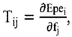 wherein 1≤i, j≤n.
 - The method according to claim 6, wherein,
when i=j, values of the elements Tii are in a range of approximately 1 nm to 5 nm; and/or
when i≠j, values of the elements Tij are in a range of approximately 0 to 1 nm. - The method according to claim 6, wherein determining the correction value of each fragment according to the effect value of the correction value of each fragment in the correction window to position errors of all fragments in the correction window and the position errors of all the fragments comprises:calculating an inverse matrix T-1 of the position disturbing matrix T; andcalculating the correction value of each fragment according to the inverse matrix T-1 and the position error of each fragment; andwherein preferably:a correction value of an ith fragment of the n fragments is Δfi = ∑j(T-1)ijΔEpej i, j = 1, 2, ...... n,wherein: ΔEpej is a position error of a jth fragment; andΔfi is the correction value of the ith fragment.
- The method according to anyone of the claims 1-8, wherein:the correction value of each fragment is less than, or equal to approximately 5 nm.
- The method according to anyone of the claims 1-9, wherein detecting the simulated exposure patterns to find out if there is at least one weak point comprises:comparing the simulated exposure patterns with the target patterns; anddetermining a certain location to be the weak point if the difference between the exposure patterns and the target patterns is greater than a threshold value.
- The method according to anyone of the claims 1-10, wherein at least one of:a shape of the correction window is one of rectangular and polygonal;an area of the correction window is in a range of approximately 200 nm×200 nm to 500 nm×500 nm; andthe weak point is at the center of the correction window.
- The method according to anyone of the claims 1, wherein:the method for correcting the target patterns includes a plurality of loops;each loop includes providing target patterns, dividing contours of the target patterns into a plurality of fragments, performing an optical proximity correction to the target patterns to obtain mask patterns, performing an optical simulation on the mask patterns to obtain simulated exposure patterns, detecting the simulated exposure patterns to find out existence of at least one weak point, determining a correction window in the target patterns according to the at least one weak point, comparing the target patterns in the correction window with patterns in a corresponding region of the simulated exposure patterns to obtain a position error of each fragment, calculating an effect value of a correction value of each fragment in the correction window on position errors of all fragments in the correction window, determining the correction value of each fragment according to the effect value of the correction value of each fragment in the correction window on position errors of all fragments in the correction window and the position error of each fragment, correcting the target patterns using the correction value of each fragment to obtain corrected target patterns value of each fragment in the correction window to position errors of all fragments in the correction window and the position errors of all the fragments, and correcting the target patterns using the correction value of each fragment to obtain corrected target patterns; andthe corrected target patterns obtained from a previous loop of the plurality of loops are used as target patterns of a next loop; andwherein preferably: the plurality of loops are ended when no weak point is found in a certain loop of the plurality of loops.
- A mask, comprising:a mask substrate; andcorrected target patterns formed on the mask substrate,wherein the corrected targeted patterns are obtained by:providing target patterns;dividing contours of target patterns into a plurality of fragments;performing an optical proximity correction on the target patterns to obtain mask patterns;performing an optical simulation on the target patterns to obtain simulated exposure patterns;detecting the simulated exposure patterns to find out existence of at least one weak point;determining a correction window in the target patterns according to the at least one weak point;comparing the target patterns in the correction window with patterns in a corresponding region of the simulated exposure patterns to obtain a position error of each fragment;calculating an effect value of a correction value of each fragment in the correction window on position errors of all fragments in the correction window;determining the correction value of each fragment according to the effect value of the correction value of each fragment in the correction window on position errors of all fragments in the correction window and the position error of each fragment; andcorrecting the target patterns using the correction value of each fragment to obtain corrected target patterns.
- The mask according to claim 13, wherein:the effect value of the correction value of each fragment in the correction window to position errors of all fragments in the correction window is obtained by calculating a position disturbing matrix of all the fragments in the correction window.
- The mask according to claim 14, wherein:the correction value of each fragment is determined by the disturbing matrix of all the fragments and the position error of each fragment.
Applications Claiming Priority (1)
| Application Number | Priority Date | Filing Date | Title |
|---|---|---|---|
| CN201610788930.7A CN107797375B (en) | 2016-08-31 | 2016-08-31 | Method for correcting target pattern |
Publications (1)
| Publication Number | Publication Date |
|---|---|
| EP3291009A1 true EP3291009A1 (en) | 2018-03-07 |
Family
ID=59677113
Family Applications (1)
| Application Number | Title | Priority Date | Filing Date |
|---|---|---|---|
| EP17186994.4A Withdrawn EP3291009A1 (en) | 2016-08-31 | 2017-08-21 | Method for correcting target patterns |
Country Status (3)
| Country | Link |
|---|---|
| US (1) | US10423062B2 (en) |
| EP (1) | EP3291009A1 (en) |
| CN (1) | CN107797375B (en) |
Families Citing this family (20)
| Publication number | Priority date | Publication date | Assignee | Title |
|---|---|---|---|---|
| US10866506B2 (en) * | 2018-10-30 | 2020-12-15 | Taiwan Semiconductor Manufacturing Co., Ltd. | Photo mask data correction method |
| CN110298834B (en) * | 2019-07-01 | 2021-03-23 | 中国电子科技集团公司第十三研究所 | Pixel-level edge effect correction method and terminal device |
| CN110426915A (en) * | 2019-08-13 | 2019-11-08 | 德淮半导体有限公司 | Optical adjacent correction method |
| CN110515267B (en) * | 2019-08-29 | 2023-08-18 | 上海华力微电子有限公司 | Layout correction method |
| CN112445059B (en) * | 2019-09-05 | 2025-01-14 | 中芯国际集成电路制造(上海)有限公司 | Optical proximity correction, photomask production and patterning method |
| CN112824972B (en) * | 2019-11-21 | 2024-06-18 | 中芯国际集成电路制造(上海)有限公司 | Target layout and mask layout correction method, mask and semiconductor structure |
| WO2021229030A1 (en) * | 2020-05-14 | 2021-11-18 | Asml Netherlands B.V. | Method for predicting stochastic contributors |
| CN111474820B (en) * | 2020-05-25 | 2023-08-11 | 上海华力集成电路制造有限公司 | Optimization method for generating simulated reentrant corner target graph |
| CN113835293B (en) * | 2020-06-24 | 2024-04-19 | 中芯国际集成电路制造(上海)有限公司 | Optical proximity correction method and mask manufacturing method |
| CN114167681B (en) * | 2020-09-10 | 2025-09-16 | 中芯国际集成电路制造(上海)有限公司 | Defect detection method, mask manufacturing method and semiconductor structure forming method |
| CN112051707A (en) * | 2020-09-25 | 2020-12-08 | 泉芯集成电路制造(济南)有限公司 | Optical proximity effect correction method and device |
| CN113759670B (en) * | 2021-08-20 | 2024-01-19 | 上海华虹宏力半导体制造有限公司 | Correction method of non-smooth OPC graph |
| CN115729028B (en) * | 2021-08-30 | 2025-09-19 | 中芯国际集成电路制造(上海)有限公司 | Optical proximity correction method and mask |
| CN115729048B (en) * | 2021-08-31 | 2026-03-06 | 上海微电子装备(集团)股份有限公司 | Methods for detecting edge placement errors |
| CN116413990B (en) * | 2021-12-31 | 2025-08-01 | 中芯国际集成电路制造(上海)有限公司 | Optical proximity correction method and system, mask, equipment and storage medium |
| CN114063384A (en) * | 2022-01-14 | 2022-02-18 | 深圳晶源信息技术有限公司 | Mask pattern correction method |
| CN115220297B (en) * | 2022-08-18 | 2026-01-09 | 上海积塔半导体有限公司 | OPC graphic correction methods, systems, and masks |
| CN116224708B (en) * | 2023-05-05 | 2023-09-12 | 合肥晶合集成电路股份有限公司 | Mask pattern correction method and device |
| CN119376173A (en) * | 2023-07-25 | 2025-01-28 | 北京超弦存储器研究院 | Optical proximity correction method and optical proximity correction system |
| CN120495136B (en) * | 2025-05-09 | 2026-04-07 | 深圳市利力中科技有限公司 | Mask pattern edge compensation correction method, system, medium and computer equipment |
Citations (5)
| Publication number | Priority date | Publication date | Assignee | Title |
|---|---|---|---|---|
| US20080098341A1 (en) * | 2006-10-20 | 2008-04-24 | Sachiko Kobayashi | Design layout generating method for semiconductor integrated circuits |
| US20120216156A1 (en) * | 2009-10-28 | 2012-08-23 | Asml Netherlands B.V. | Method of Pattern Selection for Source and Mask Optimization |
| US20150040078A1 (en) * | 2013-07-30 | 2015-02-05 | GlobalFoundries, Inc. | Methods and systems for designing and manufacturing optical lithography masks |
| US20150067619A1 (en) * | 2013-08-28 | 2015-03-05 | Macronix International Co., Ltd. | Advanced correction method |
| US20150169820A1 (en) * | 2013-12-17 | 2015-06-18 | Semiconductor Manufacturing International (Beijing) Corporation | Weak points auto-correction process for opc tape-out |
Family Cites Families (4)
| Publication number | Priority date | Publication date | Assignee | Title |
|---|---|---|---|---|
| CN100538528C (en) * | 2007-02-13 | 2009-09-09 | 中芯国际集成电路制造(上海)有限公司 | The method of optical close correction |
| CN101571669B (en) * | 2008-04-28 | 2012-12-12 | 中芯国际集成电路制造(北京)有限公司 | Method for checking optical proximity correction on the basis of model |
| CN104950568B (en) * | 2014-03-25 | 2020-02-07 | 中芯国际集成电路制造(上海)有限公司 | Optical proximity correction method and double pattern exposure method |
| CN105093810B (en) * | 2014-05-22 | 2019-09-27 | 中芯国际集成电路制造(上海)有限公司 | The method for reducing the edge position error of the optical proximity correction of critical size |
-
2016
- 2016-08-31 CN CN201610788930.7A patent/CN107797375B/en active Active
-
2017
- 2017-08-03 US US15/667,956 patent/US10423062B2/en active Active
- 2017-08-21 EP EP17186994.4A patent/EP3291009A1/en not_active Withdrawn
Patent Citations (5)
| Publication number | Priority date | Publication date | Assignee | Title |
|---|---|---|---|---|
| US20080098341A1 (en) * | 2006-10-20 | 2008-04-24 | Sachiko Kobayashi | Design layout generating method for semiconductor integrated circuits |
| US20120216156A1 (en) * | 2009-10-28 | 2012-08-23 | Asml Netherlands B.V. | Method of Pattern Selection for Source and Mask Optimization |
| US20150040078A1 (en) * | 2013-07-30 | 2015-02-05 | GlobalFoundries, Inc. | Methods and systems for designing and manufacturing optical lithography masks |
| US20150067619A1 (en) * | 2013-08-28 | 2015-03-05 | Macronix International Co., Ltd. | Advanced correction method |
| US20150169820A1 (en) * | 2013-12-17 | 2015-06-18 | Semiconductor Manufacturing International (Beijing) Corporation | Weak points auto-correction process for opc tape-out |
Also Published As
| Publication number | Publication date |
|---|---|
| CN107797375A (en) | 2018-03-13 |
| US10423062B2 (en) | 2019-09-24 |
| US20180059533A1 (en) | 2018-03-01 |
| CN107797375B (en) | 2020-11-03 |
Similar Documents
| Publication | Publication Date | Title |
|---|---|---|
| US10423062B2 (en) | Method for correcting target patterns and mask having corrected target patterns | |
| US10423063B2 (en) | Mask pattern correction method | |
| US8307310B2 (en) | Pattern generating method, method of manufacturing semiconductor device, computer program product, and pattern-shape-determination-parameter generating method | |
| US11120182B2 (en) | Methodology of incorporating wafer physical measurement with digital simulation for improving semiconductor device fabrication | |
| US8230371B2 (en) | Process-window aware detection and correction of lithographic printing issues at mask level | |
| US9508138B2 (en) | Method of detecting photolithographic hotspots | |
| US6562638B1 (en) | Integrated scheme for predicting yield of semiconductor (MOS) devices from designed layout | |
| US20070162887A1 (en) | Method of fabricating photo mask | |
| US20130302725A1 (en) | System and method for test patttern for lithography process | |
| CN110119062B (en) | Optical proximity correction method, mask manufacturing method and patterning process | |
| US20110177457A1 (en) | Mask pattern generating method, manufacturing method of semiconductor device, and computer program product | |
| CN106338883B (en) | Optical proximity correction method | |
| JP2003255509A (en) | Method of manufacturing photomask and method of manufacturing semiconductor device using the photomask | |
| US8443309B2 (en) | Multifeature test pattern for optical proximity correction model verification | |
| WO2008078213A1 (en) | A method and system for identifying weak points in an integrated circuit design | |
| US7434198B2 (en) | Method and computer program product for detecting potential failures in an integrated circuit design after optical proximity correction | |
| CN117666272A (en) | Optical proximity correction method, mask, readable storage medium and computer equipment | |
| KR20100025822A (en) | Method for decomposing mask layout and optical proximity correction using the same | |
| CN107045259B (en) | Mask plate containing monitoring pattern and monitoring method | |
| KR100807229B1 (en) | How to correct design pattern of mask | |
| US10990000B2 (en) | Photolithography plate and mask correction method | |
| JP2010122438A (en) | Method, program and device for verifying lithographic simulation model | |
| KR100861376B1 (en) | Optical proximity effect correction method using light intensity profile | |
| US8336004B2 (en) | Dimension assurance of mask using plurality of types of pattern ambient environment | |
| US20260003293A1 (en) | Method and system of correcting optical proximity correction (opc) model for manufacturing semiconductor device |
Legal Events
| Date | Code | Title | Description |
|---|---|---|---|
| PUAI | Public reference made under article 153(3) epc to a published international application that has entered the european phase |
Free format text: ORIGINAL CODE: 0009012 |
|
| STAA | Information on the status of an ep patent application or granted ep patent |
Free format text: STATUS: THE APPLICATION HAS BEEN PUBLISHED |
|
| AK | Designated contracting states |
Kind code of ref document: A1 Designated state(s): AL AT BE BG CH CY CZ DE DK EE ES FI FR GB GR HR HU IE IS IT LI LT LU LV MC MK MT NL NO PL PT RO RS SE SI SK SM TR |
|
| AX | Request for extension of the european patent |
Extension state: BA ME |
|
| STAA | Information on the status of an ep patent application or granted ep patent |
Free format text: STATUS: REQUEST FOR EXAMINATION WAS MADE |
|
| 17P | Request for examination filed |
Effective date: 20180907 |
|
| RBV | Designated contracting states (corrected) |
Designated state(s): AL AT BE BG CH CY CZ DE DK EE ES FI FR GB GR HR HU IE IS IT LI LT LU LV MC MK MT NL NO PL PT RO RS SE SI SK SM TR |
|
| RAP1 | Party data changed (applicant data changed or rights of an application transferred) |
Owner name: SEMICONDUCTOR MANUFACTURING INTERNATIONAL (BEIJING Owner name: SEMICONDUCTOR MANUFACTURING INTERNATIONAL (SHANGHA |
|
| STAA | Information on the status of an ep patent application or granted ep patent |
Free format text: STATUS: THE APPLICATION HAS BEEN WITHDRAWN |
|
| 18W | Application withdrawn |
Effective date: 20200224 |