EP3289741B1 - Skip rx during sbs transmission - Google Patents
Skip rx during sbs transmission Download PDFInfo
- Publication number
- EP3289741B1 EP3289741B1 EP16714190.2A EP16714190A EP3289741B1 EP 3289741 B1 EP3289741 B1 EP 3289741B1 EP 16714190 A EP16714190 A EP 16714190A EP 3289741 B1 EP3289741 B1 EP 3289741B1
- Authority
- EP
- European Patent Office
- Prior art keywords
- chain
- data signal
- transceiver
- wireless
- data
- Prior art date
- Legal status (The legal status is an assumption and is not a legal conclusion. Google has not performed a legal analysis and makes no representation as to the accuracy of the status listed.)
- Not-in-force
Links
- 230000005540 biological transmission Effects 0.000 title claims description 38
- 238000004891 communication Methods 0.000 claims description 32
- 238000000034 method Methods 0.000 claims description 24
- 230000000977 initiatory effect Effects 0.000 claims description 10
- 230000004044 response Effects 0.000 claims description 6
- 238000004590 computer program Methods 0.000 claims 1
- 101100161473 Arabidopsis thaliana ABCB25 gene Proteins 0.000 description 17
- 101100096893 Mus musculus Sult2a1 gene Proteins 0.000 description 17
- 101150081243 STA1 gene Proteins 0.000 description 17
- OVGWMUWIRHGGJP-WVDJAODQSA-N (z)-7-[(1s,3r,4r,5s)-3-[(e,3r)-3-hydroxyoct-1-enyl]-6-thiabicyclo[3.1.1]heptan-4-yl]hept-5-enoic acid Chemical compound OC(=O)CCC\C=C/C[C@@H]1[C@@H](/C=C/[C@H](O)CCCCC)C[C@@H]2S[C@H]1C2 OVGWMUWIRHGGJP-WVDJAODQSA-N 0.000 description 14
- 101000988961 Escherichia coli Heat-stable enterotoxin A2 Proteins 0.000 description 14
- 230000001413 cellular effect Effects 0.000 description 5
- 230000008569 process Effects 0.000 description 5
- 229920000729 poly(L-lysine) polymer Polymers 0.000 description 4
- 238000012545 processing Methods 0.000 description 4
- 102100032533 ADP/ATP translocase 1 Human genes 0.000 description 3
- 102100026396 ADP/ATP translocase 2 Human genes 0.000 description 3
- 101000768061 Escherichia phage P1 Antirepressor protein 1 Proteins 0.000 description 3
- 101000796932 Homo sapiens ADP/ATP translocase 1 Proteins 0.000 description 3
- 101000718417 Homo sapiens ADP/ATP translocase 2 Proteins 0.000 description 3
- 238000004422 calculation algorithm Methods 0.000 description 3
- 238000012986 modification Methods 0.000 description 3
- 230000004048 modification Effects 0.000 description 3
- 238000011084 recovery Methods 0.000 description 3
- 230000002411 adverse Effects 0.000 description 2
- 238000010586 diagram Methods 0.000 description 2
- 238000005516 engineering process Methods 0.000 description 2
- 238000002156 mixing Methods 0.000 description 2
- 239000002245 particle Substances 0.000 description 2
- 108700026140 MAC combination Proteins 0.000 description 1
- 230000008859 change Effects 0.000 description 1
- 238000013461 design Methods 0.000 description 1
- 230000000694 effects Effects 0.000 description 1
- 238000001914 filtration Methods 0.000 description 1
- 230000006870 function Effects 0.000 description 1
- 230000002452 interceptive effect Effects 0.000 description 1
- 230000007774 longterm Effects 0.000 description 1
- 230000007246 mechanism Effects 0.000 description 1
- 230000000116 mitigating effect Effects 0.000 description 1
- 230000003287 optical effect Effects 0.000 description 1
- 230000000630 rising effect Effects 0.000 description 1
- 238000005070 sampling Methods 0.000 description 1
- 238000013515 script Methods 0.000 description 1
Images


Classifications
-
- H—ELECTRICITY
- H04—ELECTRIC COMMUNICATION TECHNIQUE
- H04L—TRANSMISSION OF DIGITAL INFORMATION, e.g. TELEGRAPHIC COMMUNICATION
- H04L5/00—Arrangements affording multiple use of the transmission path
- H04L5/14—Two-way operation using the same type of signal, i.e. duplex
- H04L5/143—Two-way operation using the same type of signal, i.e. duplex for modulated signals
-
- H—ELECTRICITY
- H04—ELECTRIC COMMUNICATION TECHNIQUE
- H04L—TRANSMISSION OF DIGITAL INFORMATION, e.g. TELEGRAPHIC COMMUNICATION
- H04L27/00—Modulated-carrier systems
- H04L27/0008—Modulated-carrier systems arrangements for allowing a transmitter or receiver to use more than one type of modulation
-
- H—ELECTRICITY
- H04—ELECTRIC COMMUNICATION TECHNIQUE
- H04L—TRANSMISSION OF DIGITAL INFORMATION, e.g. TELEGRAPHIC COMMUNICATION
- H04L27/00—Modulated-carrier systems
- H04L27/0014—Carrier regulation
-
- H—ELECTRICITY
- H04—ELECTRIC COMMUNICATION TECHNIQUE
- H04L—TRANSMISSION OF DIGITAL INFORMATION, e.g. TELEGRAPHIC COMMUNICATION
- H04L27/00—Modulated-carrier systems
- H04L27/26—Systems using multi-frequency codes
- H04L27/2601—Multicarrier modulation systems
- H04L27/2647—Arrangements specific to the receiver only
- H04L27/2655—Synchronisation arrangements
- H04L27/2657—Carrier synchronisation
-
- H—ELECTRICITY
- H04—ELECTRIC COMMUNICATION TECHNIQUE
- H04L—TRANSMISSION OF DIGITAL INFORMATION, e.g. TELEGRAPHIC COMMUNICATION
- H04L27/00—Modulated-carrier systems
- H04L27/26—Systems using multi-frequency codes
- H04L27/2601—Multicarrier modulation systems
- H04L27/2647—Arrangements specific to the receiver only
- H04L27/2655—Synchronisation arrangements
- H04L27/2662—Symbol synchronisation
-
- H—ELECTRICITY
- H04—ELECTRIC COMMUNICATION TECHNIQUE
- H04L—TRANSMISSION OF DIGITAL INFORMATION, e.g. TELEGRAPHIC COMMUNICATION
- H04L5/00—Arrangements affording multiple use of the transmission path
- H04L5/0001—Arrangements for dividing the transmission path
- H04L5/0003—Two-dimensional division
- H04L5/0005—Time-frequency
- H04L5/0007—Time-frequency the frequencies being orthogonal, e.g. OFDM(A) or DMT
- H04L5/001—Time-frequency the frequencies being orthogonal, e.g. OFDM(A) or DMT the frequencies being arranged in component carriers
-
- H—ELECTRICITY
- H04—ELECTRIC COMMUNICATION TECHNIQUE
- H04L—TRANSMISSION OF DIGITAL INFORMATION, e.g. TELEGRAPHIC COMMUNICATION
- H04L5/00—Arrangements affording multiple use of the transmission path
- H04L5/003—Arrangements for allocating sub-channels of the transmission path
- H04L5/0058—Allocation criteria
- H04L5/0073—Allocation arrangements that take into account other cell interferences
-
- H—ELECTRICITY
- H04—ELECTRIC COMMUNICATION TECHNIQUE
- H04W—WIRELESS COMMUNICATION NETWORKS
- H04W88/00—Devices specially adapted for wireless communication networks, e.g. terminals, base stations or access point devices
- H04W88/02—Terminal devices
- H04W88/06—Terminal devices adapted for operation in multiple networks or having at least two operational modes, e.g. multi-mode terminals
Definitions
- the present embodiments relate generally to wireless networks, and specifically to transmitting and receiving wireless signals, concurrently, within the same frequency band.
- Modern wireless devices may be configured to operate in a single-band simultaneous (SBS) mode whereby the wireless device is active on multiple channels, concurrently, in the same frequency band (e.g., 2.4 GHz or 5 GHz band).
- the wireless device may include a first transceiver chain that operates on one wireless channel (e.g., Channel A) and a second transceiver chain that operates on another wireless channel (e.g., Channel B).
- the first transceiver chain may transmit data signals via Channel A while the second transceiver chain transmits data signals via Channel B, concurrently.
- the first transceiver chain may receive data signals via Channel A while the second transceiver chain receives data signals via Channel B, concurrently.
- Challenges may arise when one of the transceiver chains attempts to transmit data signals on one channel while the other transceiver chain is receiving data signals on another channel. For example, if the first transceiver chain transmits an outgoing data signal while the second transceiver chain is receiving an incoming data signal, the transmission of the outgoing data signal may interfere with the reception of the incoming data signal. This phenomenon, commonly known as "self-interference," typically occurs when the first and second transceiver chains are located in relatively close proximity of one another. Due to the close proximity of the transceiver chains, the signal strength of the outgoing data signal may be significantly greater than the signal strength of the incoming data signal (e.g., as viewed by a receive chain of the second transceiver chain). As a result, the second transceiver chain may not only fail to receive incoming data signals that directly overlap with the outgoing data signal, but may also fail to receive incoming data signals that arrive after transmission of the outgoing data signals ends.
- self-interference typically occurs when the first and second transce
- US 2012/0121049 A1 discloses methods for accelerating a fine carrier phase and frequency offset recovery algorithm in a receiver of a communication system.
- a wireless device receives a first data signal via a first transceiver chain while concurrently initiating a transmission of a second data signal via a second transceiver chain.
- the wireless device Upon initiating the transmission of the second data signal, the wireless device suspends updates to one or more tracking loops of the first transceiver chain. The updates to the one or more tracking loops may be suspended prior to transmitting the second data signals from the second transceiver chain.
- the one or more tracking loops may be used in recovering a set of data from the received first data signal. Further, the updates to the one or more tracking loops may be based at least in part on the received first data signal.
- the one or more tracking loops may include a delay-locked loop (DLL) circuit.
- the one or more tracking loops may include a phase-locked loop (PLL) circuit.
- the wireless device may subsequently resume updates to the one or more tracking loops of the first transceiver chain after completing the transmission of the second data signal.
- the first data signal may be received on a first wireless channel of a first frequency band and the second data signal may be transmitted on a second wireless channel of the first frequency band.
- the first data signal may be received in accordance with a first wireless protocol and the second data signal may be transmitted in accordance with a second wireless protocol that is different than the first wireless protocol.
- the first wireless protocol may be a wireless local area network (WLAN) protocol and the second wireless protocol may be a Bluetooth® protocol.
- the first wireless protocol may be a Bluetooth® protocol and the second wireless protocol may be a WLAN protocol.
- the example embodiments allow a wireless communications device to transmit and receive wireless data signals on two or more channels of the same frequency band, concurrently, while mitigating the effects of self-interference. For example, by suspending updates to one or more tracking loops of a first transceiver chain while a second transceiver chain transmits outgoing data signals, the tracking loops may remain unaffected by self-interference caused by the transmission of outgoing data signals. The tracking loops may immediately resume tracking incoming data signals once the transmission of outgoing data signals is completed.
- Wi-Fi wireless local area network
- Wi-Fi wireless local area network
- Wi-Fi can include communications governed by the IEEE 802.11 standards, Bluetooth®, HiperLAN (a set of wireless standards, comparable to the IEEE 802.11 standards, used primarily in Europe), and other technologies used in wireless communications.
- Wi-Fi wireless local area network
- the example embodiments are equally applicable to other WLAN systems including, for example, multiple WLANs, peer-to-peer (or Independent Basic Service Set) systems, Wi-Fi Direct systems, and/or Hotspots.
- the example embodiments may be applied to the exchange of any data unit, packet, and/or frame between wireless devices.
- the term "frame” may include any frame, packet, or data unit such as, for example, protocol data units (PDUs), MAC protocol data units (MPDUs), and physical layer convergence procedure protocol data units (PPDUs).
- PDUs protocol data units
- MPDUs MAC protocol data units
- PPDUs physical layer convergence procedure protocol data units
- A-MPDU may refer to aggregated MPDUs.
- Each of the buses may alternatively be a single signal line, and each of the single signal lines may alternatively be buses, and a single line or bus might represent any one or more of a myriad of physical or logical mechanisms for communication between components.
- Embodiments of this disclosure are not to be construed as limited to specific examples described herein but rather to include within their scope all embodiments defined by the appended claims.
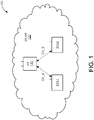
- FIG. 1 shows an example wireless system 100 within which the example embodiments may be implemented.
- the wireless system 100 is shown to include two wireless stations STA1 and STA2, a wireless access point (AP) 110, and a wireless local area network (WLAN) 120.
- the WLAN 120 may be formed by a plurality of Wi-Fi access points (APs) that may operate according to the IEEE 802.11 family of standards (or according to other suitable wireless protocols).
- APs Wi-Fi access points
- WLAN 120 may be formed by any number of access points such as AP 110.
- the AP 110 is assigned a unique MAC address that is programmed therein by, for example, the manufacturer of the access point.
- each of STA1 and STA2 is also assigned a unique MAC address.
- Each of the stations STA1 and STA2 may be any suitable Wi-Fi enabled wireless device including, for example, a cell phone, personal digital assistant (PDA), tablet device, laptop computer, or the like.
- Each station (STA) may also be referred to as user equipment (UE), a subscriber station, a mobile unit, a subscriber unit, a wireless unit, a remote unit, a mobile device, a wireless device, a wireless communications device, a remote device, a mobile subscriber station, an access terminal, a mobile terminal, a wireless terminal, a remote terminal, a handset, a user agent, a mobile client, a client, or some other suitable terminology.
- UE user equipment
- each STA may include one or more transceivers, one or more processing resources (e.g., processors and/or ASICs), one or more memory resources, and a power source (e.g., a battery).
- the memory resources may include a non-transitory computer-readable medium (e.g., one or more nonvolatile memory elements, such as EPROM, EEPROM, Flash memory, a hard drive, etc.) that store instructions for performing operations described below with respect to FIGS. 7 and 8 .
- the one or more transceivers may include Wi-Fi transceivers, Bluetooth® transceivers, cellular transceivers, and/or other suitable radio frequency (RF) transceivers (not shown for simplicity) to transmit and receive wireless communication signals.
- Each transceiver may communicate with other wireless devices in distinct operating frequency bands and/or using distinct communications protocols.
- the Wi-Fi transceiver may communicate within a 2.4 GHz frequency band and/or within a 5 GHz frequency band in accordance with the IEEE 802.11 specification.
- the cellular transceiver may communicate within various RF frequency bands in accordance with a 4G Long Term Evolution (LTE) protocol described by the 3 rd Generation Partnership Project (3GPP) (e.g., between approximately 700 MHz and approximately 3.9 GHz) and/or in accordance with other cellular protocols (e.g., a Global System for Mobile (GSM) communications protocol).
- LTE Long Term Evolution
- 3GPP 3 rd Generation Partnership Project
- GSM Global System for Mobile
- the transceivers included within stations STA1 and STA2 may be any technically feasible transceiver such as a ZigBee transceiver described by the ZigBee specification, a Wi-Gig transceiver, and/or a HomePlug transceiver described by a specification from the HomePlug Alliance.
- two or more transceivers of the same station may communicate within the same frequency band, simultaneously (e.g., with each transceiver operating on a different channel of the frequency band).
- the AP 110 may be any suitable device that allows one or more wireless devices to connect to a network (e.g., a local area network (LAN), wide area network (WAN), metropolitan area network (MAN), and/or the Internet) via AP 110 using Wi-Fi, Bluetooth®, or any other suitable wireless communication standards.
- a network e.g., a local area network (LAN), wide area network (WAN), metropolitan area network (MAN), and/or the Internet
- the AP 110 may include one or more transceivers, a network interface, one or more processing resources, and one or more memory resources.
- the one or more transceivers may include Wi-Fi transceivers, Bluetooth® transceivers, cellular transceivers, and/or other suitable RF transceivers (not shown for simplicity) to transmit and receive wireless communication signals.
- Each transceiver may communicate with other wireless devices in distinct operating frequency bands and/or using distinct communication protocols.
- two or more transceivers of the AP 110 may communicate within the same frequency band, simultaneously (e.g., with each transceiver operating on a different channel of the frequency band).
- the memory resources may include a non-transitory computer-readable medium (e.g., one or more nonvolatile memory elements, such as EPROM, EEPROM, Flash memory, a hard drive, etc.) that stores instructions for performing operations described below with respect to FIGS. 7 and 8 .
- the AP 110 may be configured to communicate with both of the stations STA1 and STA2, concurrently, in the same frequency band. This mode of operation may be referred to herein as "single-band simultaneous" (SBS).
- the AP 110 may include multiple transceivers or transceiver chains (not shown for simplicity) that operate on (e.g., communicate over) different channels of the same frequency band.
- one of the transceiver chains may communicate with STA1 over a first wireless channel (CH_A) and another one of the transceiver chains may communicate with STA2 over a second wireless channel (CH_B).
- CH_A first wireless channel
- CH_B second wireless channel
- the AP's transceiver chains may operate on non-overlapping channels of the frequency band.
- channel CH_A corresponds to channel 1 of the 2.4 GHz frequency band
- channel CH_B may correspond to any of channels 6-11 of the 2.4 GHz frequency band (e.g., because for the 2.4 GHz frequency band, channels 6-11 do not overlap channel 1).
- the AP 110 may transmit data signals to both of the stations STA1 and STA2, concurrently, with little or no interference between the channels (e.g., especially when the signals are transmitted to STA1 and STA2 on non-overlapping channels).
- the AP 110 may also receive data signals from both of the stations STA1 and STA2, concurrently, with little or no interference between the channels.
- complications may arise when the AP 110 attempts to transmit a data signal over one channel while concurrently receiving a data signal over the other channel. For example, as perceived by the AP 110, outgoing data signals transmitted by one of its transceiver chains may be much stronger than incoming data signals received by another of its transceiver chains (e.g., which are generally weakened due to path loss).
- the transceiver chain receiving the incoming data signals may undesirably sample and/or "track" (e.g., by adjusting the phase, frequency, delay, and/or other timing information used in the reception of incoming data signals) at least a portion of the outgoing data signals being transmitted by the other transceiver chain.
- the AP 110 may track a channel using pilot tones in each received data symbol.
- the AP 110 may calculate a frequency offset based on the received data signals and the pilot tones.
- the AP 110 may also estimate a phase offset corresponding with a change in phase of the received data signals.
- the AP 110 may then use the phase offset and/or frequency offset to correct the received data tones in one or more tracking loops (e.g., DLLs, PLLs, and/or other components that may track the incoming data signal).
- the calculated phase and/or frequency offsets may be distorted due to self-interference at the AP 110 (e.g., when the AP 110 attempts to transmit and receive data signals concurrently).
- the AP 110 may apply incorrect modifications to the received data signals.
- the tracking loops in the AP 110 may enter an incorrect state, thereby causing subsequent PDUs of the incoming data signals to receive improper modifications even after the AP 110 has completed its transmission on the other wireless channel.
- the AP 110 may prevent a first transceiver chain (e.g., that is receiving an incoming data signal) from tracking outgoing data signals transmitted by a second transceiver chain, for example, by suspending or disabling updates to one or more tracking loops (e.g., DLLs, PLLs, and/or other components that may track the incoming data signal) within the first transceiver chain.
- a first transceiver chain e.g., that is receiving an incoming data signal
- one or more tracking loops e.g., DLLs, PLLs, and/or other components that may track the incoming data signal
- This technique may be referred to herein as "receive skipping.” For example, upon detecting that at least one of its transceiver chains is about to transmit an outgoing data signal while another of its transceiver chains is receiving an incoming data signal, the AP 110 may suspend updating one or more tracking loops of the receiving transceiver chain prior to the transmission of the outgoing data signal. The AP 110 may then resume updating the tracking loops of the receiving transceiver chain after the transmission of the outgoing data signal is completed. Upon resuming updates, the tracking loops may quickly lock back onto the incoming data signal (e.g., because the tracking loops were not adversely affected by the outgoing data signal).
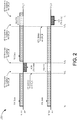
- FIG. 2 shows an example timing diagram 200 depicting an SBS wireless communication with receive (RX) skipping during concurrent transmission and reception of data signals.
- the AP and stations STA1-STA2 of FIG. 2 may be AP 110 and stations STA1-STA2, respectively, of FIG. 1 .
- the AP 110 receives incoming (RX) data signals from both of the stations STA1 and STA2 (e.g., over wireless channels CH_A and CH_B, respectively).
- the RX data signals may correspond to a number of data frames that each include a number of individual protocol data units (PDUs) (not shown for simplicity).
- PDUs protocol data units
- time t 1 the AP 110 stops receiving RX data signals from STA1, and initiates a transmission (TX) event on channel CH_A.
- time t 1 may coincide with the end of a data frame transmitted by STA1 (e.g., for which STA1 expects to receive an acknowledgement (ACK) frame from the AP 110).
- ACK acknowledgement
- the AP 110 Upon initiating the TX event on channel CH_A, the AP 110 suspends tracking loop (TL) updates for its transceiver chain operating on channel CH_B at time t 2 . At substantially the same time (e.g., time t 2 ), or immediately thereafter, the AP 110 transmits an outgoing (TX) data signal on channel CH_A.
- the TX data signal may be an ACK frame confirming receipt of data transmitted by STA1.
- the tracking loop updates may remain suspended for the duration of the TX data transmission (e.g., from time t 2 to t 3 ).
- the AP 110 may immediately resume updating the tracking loops of the transceiver chain operating on channel CH_B. Accordingly, the AP 110 may "skip" receiving a portion of the RX data signals on channel CH_B (e.g., which may include one or more PDUs) that overlaps with the TX data signal transmitted on channel CH_A (e.g., from time t 2 to time t 3 ), for example, because the overlapping portion is likely to be altered or otherwise affected by the TX data signal.
- CH_B e.g., which may include one or more PDUs
- the AP 110 once again begins receiving RX data signals from STA1. Then, at time t 5 , the AP 110 stops receiving RX data signals from STA2, and initiates a TX event on channel CH_B. Upon initiating the TX event on channel CH_B, the AP 110 suspends tracking loop updates for its transceiver chain operating on channel CH_A at time t 6 . At substantially the same time (e.g., time t 6 ), or immediately thereafter, the AP 110 transmits a TX data signal on channel CH_B. For example, the TX data signal may be an ACK frame confirming receipt data transmitted by STA2.
- the tracking loop updates may remain suspended for the duration of the TX data transmission (e.g., from time t 6 to time t 7 ).
- the AP 110 may immediately resume updating the tracking loops of its transceiver chain operating on channel CH_A.
- SBS communications are performed by the AP 110 with respect to multiple STAs.
- any of the stations STA1 and/or STA2 may be operable in an SBS mode, whereby the STA may communicate with multiple APs and/or other STAs, simultaneously, within the same frequency band.
- a wireless device e.g., an AP or a STA
- two wireless devices may be enabled for full duplex communications with one another (e.g., for peer-to-peer communications).
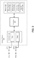
- FIG. 3 shows a wireless device 300 in accordance with example embodiments.
- the wireless device 300 may be one embodiment of the AP 110 and/or any of the stations STA1-STA2 of FIG. 1 .
- the wireless device 300 includes at least a transceiver 310, a processor 320, a memory 330, a first antenna ANT1, and a second antenna ANT2.
- the transceiver 310 may be coupled to antennas ANT1-ANT2 either directly or through an antenna selection circuit (not shown for simplicity).
- the transceiver 310 may be used to transmit signals to and receive signals from access points, STAs, and/or other suitable wireless devices.
- the transceiver 310 may also be used to scan the surrounding environment to detect and identify nearby access points and/or STAs.
- the transceiver 310 is shown to include two transceiver chains TRX1 and TRX2 that may be used to communicate wirelessly with other suitable wireless devices (e.g., including wireless access points and/or wireless stations).
- the first transceiver chain TRX1 may include a first transmit chain to process and transmit signals to another wireless device via antenna ANT1, and may include a first receive chain to process signals received via antenna ANT1.
- the second transceiver chain TRX2 may include a second transmit chain to process and transmit signals to another wireless device via antenna ANT2, and may include a second receive chain to process signals received via antenna ANT2.
- each of the transceiver chains TRX1 and TRX2 may be configured to operate on a different channel of a given frequency band (e.g., in SBS mode).
- the transceiver chains TRX1 and TRX2 may be configured to transmit and/or receive data signals over respective channels CH_A and CH_B of the same frequency band.
- Transceiver 310 is depicted in FIG. 3 as including only two transceiver chains TRX1 and TRX2 and two antennas ANT1-ANT2 for simplicity only; for other embodiments, transceiver 310 may include any suitable number of transceiver chains TRX that may be coupled to any suitable number of antennas.
- the wireless device 300 may be configured for multiple-input, multiple-output (MIMO) operations.
- the MIMO operations may include single-user MIMO (SU-MIMO) operations and multi-user MIMO (MU-MIMO) operations.
- Processor 320 which is coupled to transceiver 310 and memory 330, may be any suitable one or more processors capable of executing scripts or instructions of one or more software programs stored in the wireless device 300 (e.g., within memory 330).
- processor 320 is shown in FIG. 3 as being coupled between transceiver 310 and memory 330.
- transceiver 310, processor 320, and/or memory 330 may be connected together using one or more buses (not shown for simplicity).
- Memory 330 may include TRX1 packet queues 332 and TRX2 packet queues 334.
- the TRX1 packet queues 332 may store data packets and/or frames to be transmitted from the wireless device 300, via channel CH_A, to one or more receiving devices.
- the TRX2 packet queues 334 may store data packets and/or frames to be transmitted from the wireless device 300, via channel CH_B, to one or more receiving devices.
- Memory 330 may also include a non-transitory computer-readable medium (e.g., one or more non-volatile memory elements, such as EPROM, EEPROM, Flash memory, a hard drive, etc.) that may store the following software modules:
- a non-transitory computer-readable medium e.g., one or more non-volatile memory elements, such as EPROM, EEPROM, Flash memory, a hard drive, etc.
- FIG. 4 shows an example transceiver (TRX) circuit 400 that may be operable for SBS wireless communications.
- the TRX circuit 400 may be implemented by a wireless device (e.g., such as the AP 110 and/or stations STA1 and STA2) to transmit and receive data signals over a wireless medium.
- the TRX circuit 400 may be one embodiment of the transceiver 310 of FIG. 3 .
- the TRX circuit 400 includes at least two TRX chains 410 and 420. Although only the transmit (TX) circuitry (e.g., elements 411-418) of TRX chain 410 is shown in the example of FIG. 4 , the TRX chain 410 may also include receive (RX) circuitry (not shown for simplicity).
- TX transmit
- RX receive
- TRX chain 420 may also include TX circuitry (not shown for simplicity).
- the two TRX chains 410 and 420 may reside on separate die and/or integrated circuits (ICs).
- the first TRX chain 410 may include a digital signal processing (DSP) circuit 411, a digital-to-analog converter (DAC) 412, a TX filter 414, a frequency synthesizer 415, a mixer 416, and a power amplifier (PA) 418.
- the TX circuitry 411-418 may be used for transmitting outgoing (TX) data signals to another device (not shown).
- the DSP circuit 411 may convert a set of TX data to a digital data stream.
- the DAC 412 may convert the digital data stream to an analog data signal, which is filtered by the TX filter 414.
- the filtered analog data signal is then up-converted to a carrier frequency by the mixer 416, for example, by mixing the analog data signal with a local oscillator signal (LO A ) generated by the frequency synthesizer 415.
- the up-converted analog signal is amplified by the PA 418 and subsequently transmitted onto the wireless medium via antenna ANT as a TX data signal.
- the second TRX chain 420 may include a DSP circuit 421, an analog-to-digital converter (ADC) 422, an RX filter 424, a frequency synthesizer 425, a mixer 426, and a low-noise amplifier (LNA) 428.
- the RX circuitry 421-428 may be used for receiving incoming (RX) data signals transmitted by another device (not shown).
- the LNA 428 amplifies a signal (e.g., RX data signal) received by antenna ANT, and forwards the received signal to the mixer 426.
- the mixer 426 down-converts the RX data signal, for example, by mixing the RX data signal with a local oscillator signal (LO B ) generated by the frequency synthesizer 425.
- the data signal may be filtered by the RX filter 424 and converted to a digital data stream via the ADC 422.
- the digital data stream may then be processed by the DSP circuit 421 to recover a set of RX data.
- the DSP circuits 411 and 421 are depicted in the example implementation of FIG. 4 as being included within TRX chains 410 and 420, respectively, for other implementations, the DSP circuits 411 and 421 may be separate from the transceiver circuit 400. Further, for at least some implementations, the DSP circuits 411 and 421 may correspond to a baseband processor (not shown for simplicity) of the wireless device 300 of FIG. 3 .
- the TRX circuit 400 may be configured to operate in SBS mode.
- the first TRX chain 410 may be configured to transmit TX data signals over a first wireless channel (e.g., channel CH_A) while the second TRX chain 420 receives RX data signals over a second wireless channel (e.g., channel CH_B) within the same frequency band.
- the TRX chain 420 may be configured to receive the RX data signals concurrently while a third TRX chain (not shown for simplicity) transmits TX data signals over another wireless channel (e.g., channel CH_C) within the same frequency band.
- the TRX circuit 400 may suspend updating one or more tracking loops within the second TRX chain 420 when performing concurrent transmit and receive operations.
- a processor or controller within the wireless device and/or within the TRX circuit 400 may monitor outgoing data transmissions by the first TRX chain 410. More specifically, the controller may detect when the first TRX chain 410 becomes active (e.g., indicating the start of a TX event), and may assert a Skip_RX signal upon initiation of the TX event. The Skip_RX signal may be used to suspend updates to one or more tracking loops within the DSP circuit 421 and/or the ADC 422 of the second TRX chain 420.
- RX data signals are sent without corresponding clock signals.
- the ADC 422 may sample the received data signals based on a locally-generated clock signal recovered from the received data signals.
- the local clock signal may be periodically updated to track the received data signals.
- the ADC 422 may suspend updating its local clock signal, for example, to ensure that it does not track a TX data signal being transmitted by the first TRX chain 410.
- the DSP circuit 421 may include circuitry for filtering, recovering, converting, and/or otherwise processing digital data received via the second TRX chain 420.
- the DSP circuit 421 may include PLLs, DLLs, and/or other circuitry (not shown in FIG. 4 ) that tracks the received data signal.
- the DSP circuit 421 may also suspend updating any tracking loops that track or otherwise depend upon the received data signal.
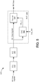
- FIG. 5 shows an example TRX chain 500 with RX skipping functionality.
- the TRX chain 500 may be one embodiment of the second TRX chain 420 of FIG. 4 .
- the TRX chain 500 includes an analog front end (AFE) 510, an equalizer (EQ) 520, and an ADC 530.
- the AFE 510 may include circuitry (e.g., the RX filter 424, mixer 426, and/or LNA 428 of FIG. 4 ) for receiving RX data signals from another wireless device (not shown for simplicity).
- the equalizer 520 mitigates (e.g., reduces and/or eliminates) intersymbol interference (ISI) in the RX data signals
- the ADC 530 converts the RX data signals from the analog domain to the digital domain.
- ISI intersymbol interference
- the ADC 530 may include a clock recovery circuit (CRC) 532 and a sampler 534.
- the sampler 534 may convert the RX data signals to a digital (RX) data stream by sampling the RX data signals using a local receive clock (RX_clk) signal generated by the CRC 532.
- the CRC 532 tracks a phase of the RX data signals to ensure that the RX_clk signal is phase-aligned with the RX data signals. More specifically, the CRC 532 may periodically (e.g., continuously) extract phase and/or frequency information from the RX data signals, and may adjust a phase and/or frequency of the RX_clk signal based on the extracted phase and frequency information.
- the CRC 532 may suspend updating the RX_clk signal when the Skip_RX signal is asserted. For example, upon receiving an asserted Skip_RX signal, the CRC 532 may maintain a current state of the RX_clk signal, without adjusting for phase and/or frequency discrepancies in the RX data signals. When the Skip_RX signal is deasserted, the CRC 532 may resume updating the RX_clk signal based on the RX data signals. By suspending updates to the RX_clk signal, the RX_clk signal may remain unaffected by outgoing data signals concurrently transmitted by a transmit chain of the same wireless device (e.g., TRX chain 410 of FIG. 4 ). Accordingly, the RX_clk signal may quickly reestablish phase and/or frequency alignment with the RX data signal when the Skip_RX signal is deasserted.
- a transmit chain of the same wireless device e.g., TRX chain 410 of FIG. 4
- FIG. 6 shows an example CRC 600 that may suspend updating an output clock signal when operating in an RX skipping mode.
- the CRC 600 may be one embodiment of CRC 532 of FIG. 5 .
- the CRC 600 includes a phase and frequency detector (PFD) 610, a charge pump 620, a loop filter 630, a voltage-controlled oscillator (VCO) 640, and a frequency divider 650.
- the CRC 600 receives the RX data signals (e.g., as a reference clock signal) and generates the RX_clk signal based on the RX data signals.
- PFD phase and frequency detector
- VCO voltage-controlled oscillator
- the CRC 600 may periodically adjust a phase and/or frequency of the RX_clk signal based at least in part on detected changes in the phase and/or frequency of the RX data signals.
- the RX_clk signal effectively tracks (e.g., is phase-aligned and/or frequency-aligned with) the RX data signal.
- the PFD 610 may compare the relative timing (e.g., phase difference) between rising and/or falling edges of the RX data signal and a feedback (FB) signal to generate "up” (UP) and “down” (DN) control signals.
- the charge pump 620 may convert the UP and DN control signals to a charge (Qc) that is proportional to the phase difference between the RX data and FB signals.
- the charge Q C is filtered (e.g., integrated) by the loop filter 630 and provided as a control voltage (V C ) to the VCO 640.
- the VCO 640 generates RX_clk (e.g., as an oscillator signal) having a frequency based on the control voltage V C .
- the RX_clk signal may be passed through a frequency divider 650 (e.g., to scale the frequency of the RX_clk signal to that of the RX data signal) and provided to the PFD 610 as the FB signal.
- the CRC 600 may suspend updating the RX_clk signal in response to the Skip_RX signal.
- assertion of the Skip_RX signal may cause the charge pump 620 to hold its present charge Qc.
- the charge pump 620 may stop responding to the UP and DN control signals once it detects that the Skip_RX signal has been asserted.
- the control voltage V C is also held constant, thereby causing the VCO 640 to maintain the RX_clk signal in its current state. This may effectively prevent the RX_clk signal from tracking the RX data signal for the duration that the Skip_RX signal is asserted.
- the charge pump 620 may resume updating its output charge Q C in response to UP and DN control signals from the PFD 610.
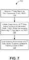
- FIG. 7 shows a flowchart depicting an example RX skipping operation 700.
- the example operation 700 may be performed by the wireless device 300 to suspend updates to one or more tracking loops of a transceiver (TRX) chain when operating in SBS mode.
- the wireless device 300 receives a first data signal via a first TRX chain (TRX1) of the transceiver 310 (710).
- the first data signal may be sent over a particular wireless channel (e.g., CH_A).
- the transceiver chains TRX1 and TRX2 may operate on separate wireless channels CH_A and CH_B, respectively.
- the wireless device 300 then initiates a transmission of a second data signal via a second TRX chain (TRX2) of the transceiver 310 while concurrently receiving the first data signal via TRX1 (720).
- the second data signal may be scheduled to be transmitted over a different wireless channel (e.g., CH_B) than the first data signal.
- the processor 320 in executing the TX control module 336, may determine that the TX circuitry of the second transceiver chain TRX2 has been activated and/or that a TX event has been initiated on TRX2.
- the TX event may correspond with a transmission of buffered TX data from the TRX2 packet queues 334.
- the TX event may correspond with a transmission of a management frame (e.g., a beacon frame) or a control frame (e.g., an ACK frame).
- the wireless device 300 Upon initiating the transmission of the second data signal, the wireless device 300 suspends updates to one or more tracking loops of the first transceiver chain TRX1 (730).
- the TX control module 336 may cause the processor 320 to execute the skip RX module 338 upon determining that the TX circuitry of the second transceiver chain TRX2 has been activated (e.g., is preparing to transmit data signals).
- the processor 320 in executing the skip RX module 338, may prevent the first transceiver chain TRX1 from updating its tracking loops (e.g., that track the first data signal) until the second transceiver chain TRX2 has finished transmitting the second data signal.
- the skip RX module 338 may assert the Skip_RX signal during transmission of the second data signal.
- the processor 320 in executing the skip RX module 338, may subsequently allow the first transceiver chain TRX1 to resume updating its tracking loops once the transmission of the second data signal has been completed.
- FIG. 8 shows a flowchart depicting an SBS communication operation 800 in accordance with example embodiments.
- the operation 800 may be performed by the TRX circuit 400 to transmit and receive data signals, concurrently, in the same frequency band.
- the TRX circuit 400 receives an incoming (RX) data signal via an active TRX chain (810).
- the active TRX chain may correspond with the second TRX chain 420.
- the second TRX chain 420 may operate on a first wireless channel of a particular frequency band.
- a TX event may correspond to a transmission of outgoing (TX) data signals (e.g., which may include buffered data frames, management frames, and/or control frames) via the first TRX chain 410.
- TX outgoing
- the first TRX chain 410 may operate on a second wireless channel of the same frequency band on which the second TRX chain 420 operates (e.g., although the second wireless channel may be different than the first wireless channel).
- the second TRX chain 420 may continue to receive RX data without interruption (810).
- the TRX circuit 400 may suspend updating one or more tracking loops of the active TRX chain (830). For example, the TRX circuit 400 may assert the Skip_RX signal to cause the ADC 422 and/or the DSP circuit 421 to hold or otherwise maintain a current state of their tracking loops (e.g., PLLs, DLLs, and/or other circuitry that tracks the RX data signal).
- the first TRX chain 410 may begin transmitting the TX data signals over the second wireless channel (840). As described above, with respect to FIG. 6 , suspending updates to a tracking loop in the second TRX chain 420 may prevent the tracking loop from tracking or locking to a phase and/or frequency of the TX data signals while the Skip_RX signal is asserted.
- the TRX circuit 400 may then determine whether the TX event has been completed (850).
- the TX event may last a predetermined duration (e.g., the transmission of a fixed-size data frame, management frame, and/or control frame).
- the TRX circuit 400 may continue to monitor the first TRX chain 410 to determine when the TX event is over (e.g., when the TRX chain 410 becomes inactive and/or stops transmitting TX data signals). As long as the first TRX chain 410 is still transmitting TX data signals (as tested at 850), the second TRX chain 420 may continue to suspend updating its tracking loops (830).
- the second TRX chain 420 may then resume updating its tracking loops (860). For example, the TRX circuit 400 may deassert the Skip_RX signal, which returns the ADC 422 and/or the DSP circuit 421 to normal modes of operation. Moreover, because the tracking loops in the second TRX chain 420 may remain unaffected by the TX data signals that were concurrently transmitted by the first TRX chain 410, the tracking loops may quickly lock back onto the phase and/or frequency of the RX data signals once updating is resumed (e.g., because the tracking loops were not adversely affected by outgoing data transmissions).
- a software module may reside in RAM memory, flash memory, ROM memory, EPROM memory, EEPROM memory, registers, hard disk, a removable disk, a CD-ROM, or any other form of storage medium known in the art.
- An exemplary storage medium is coupled to the processor such that the processor can read information from, and write information to, the storage medium. In the alternative, the storage medium may be integral to the processor.
Landscapes
- Engineering & Computer Science (AREA)
- Signal Processing (AREA)
- Computer Networks & Wireless Communication (AREA)
- Mobile Radio Communication Systems (AREA)
Applications Claiming Priority (2)
| Application Number | Priority Date | Filing Date | Title |
|---|---|---|---|
| US14/696,952 US10021736B2 (en) | 2015-04-27 | 2015-04-27 | Skip RX during SBS transmission |
| PCT/US2016/023971 WO2016175948A1 (en) | 2015-04-27 | 2016-03-24 | Skip rx during sbs transmission |
Publications (2)
| Publication Number | Publication Date |
|---|---|
| EP3289741A1 EP3289741A1 (en) | 2018-03-07 |
| EP3289741B1 true EP3289741B1 (en) | 2018-11-14 |
Family
ID=55650780
Family Applications (1)
| Application Number | Title | Priority Date | Filing Date |
|---|---|---|---|
| EP16714190.2A Not-in-force EP3289741B1 (en) | 2015-04-27 | 2016-03-24 | Skip rx during sbs transmission |
Country Status (6)
| Country | Link |
|---|---|
| US (1) | US10021736B2 (enExample) |
| EP (1) | EP3289741B1 (enExample) |
| JP (1) | JP2018524834A (enExample) |
| KR (1) | KR101912187B1 (enExample) |
| CN (1) | CN107534639A (enExample) |
| WO (1) | WO2016175948A1 (enExample) |
Families Citing this family (2)
| Publication number | Priority date | Publication date | Assignee | Title |
|---|---|---|---|---|
| US9819477B2 (en) | 2015-04-30 | 2017-11-14 | Qualcomm Incorporated | Align transmissions for SBS |
| CN115299013B (zh) * | 2020-03-26 | 2024-02-09 | 华为技术有限公司 | 一种信道跟踪方法及其相关设备 |
Family Cites Families (23)
| Publication number | Priority date | Publication date | Assignee | Title |
|---|---|---|---|---|
| JP3028802B2 (ja) * | 1998-05-28 | 2000-04-04 | 日本電気株式会社 | Cdma移動通信システムにおける呼出捕捉時の電力制御方法 |
| GB2342009A (en) | 1998-09-24 | 2000-03-29 | Nokia Mobile Phones Ltd | Disabling a PLL to reduce power consumption in a receiver |
| US7327754B2 (en) * | 2000-09-28 | 2008-02-05 | Teridian Semiconductor, Corp. | Apparatus and method for freezing the states of a receiver during silent line state operation of a network device |
| TWI234943B (en) * | 2002-08-14 | 2005-06-21 | Intel Corp | Method and apparatus for mitigating radio frequency interference between transceiver systems |
| CA2598019C (en) * | 2005-02-16 | 2013-04-30 | Qualcomm Incorporated | Low duty cycle half-duplex mode operation with communication device |
| JP2007150829A (ja) * | 2005-11-29 | 2007-06-14 | Kyocera Corp | 無線装置及び通信制御方法 |
| US7769375B2 (en) * | 2006-02-09 | 2010-08-03 | Eagle River Holdings Llc | System and method for communication utilizing time division duplexing |
| US8976727B2 (en) | 2006-10-22 | 2015-03-10 | Viasat, Inc. | Cyclical obstruction communication system |
| US20080111599A1 (en) * | 2006-11-14 | 2008-05-15 | Rajendran Nair | Wideband dual-loop data recovery DLL architecture |
| US7940809B2 (en) * | 2007-04-09 | 2011-05-10 | Synerchip Co. Ltd. | Digital video interface with bi-directional half-duplex clock channel used as auxiliary data channel |
| US8031646B2 (en) * | 2007-05-15 | 2011-10-04 | Atc Technologies, Llc | Systems, methods and devices for reusing spectrum of another operator |
| US8880004B2 (en) * | 2009-05-14 | 2014-11-04 | Qualcomm Incorporated | System and method for resolving conflicts between air interfaces in a wireless communication system |
| US8848771B2 (en) * | 2009-05-14 | 2014-09-30 | Qualcomm Incorporated | System and method for simultaneous operation of multiple modems using a single transceiver |
| TWI389530B (zh) * | 2009-08-04 | 2013-03-11 | Ralink Technology Corp | 用於通訊系統之接收器的初始化方法與時序回復器 |
| US9179395B2 (en) | 2010-01-18 | 2015-11-03 | Qualcomm Incorporated | Method and apparatus for mitigating data loss during autonomous system information reading |
| US9282462B2 (en) * | 2010-03-31 | 2016-03-08 | Qualcomm Incorporated | Method and apparatus to facilitate support for multi-radio coexistence |
| US9246603B2 (en) * | 2010-08-12 | 2016-01-26 | Mediatek Inc. | Method of in-device interference mitigation for cellular, bluetooth, WiFi, and satellite systems coexistence |
| US20120121049A1 (en) | 2010-11-12 | 2012-05-17 | Ayham Al-Banna | Initial phase estimator to accelerate carrier phase recovery |
| US9414372B2 (en) | 2012-03-16 | 2016-08-09 | Qualcomm Incorporated | Digital filter control for filter tracking speedup |
| US9154983B2 (en) | 2013-01-14 | 2015-10-06 | Qualcomm Incorporated | Systems and methods for detecting or signaling the presence of bursty interference on wireless networks |
| US9882593B2 (en) * | 2013-05-30 | 2018-01-30 | Celeno Communications (Israel) Ltd. | Coexistence between primary chains and auxiliary receiver chain in a WLAN device |
| US9402199B2 (en) * | 2013-10-14 | 2016-07-26 | Netgear, Inc. | Systems and methods for wireless load balancing and channel selection for a wireless device using WLAN modules operating simultaneously in different wireless bands |
| US9819477B2 (en) | 2015-04-30 | 2017-11-14 | Qualcomm Incorporated | Align transmissions for SBS |
-
2015
- 2015-04-27 US US14/696,952 patent/US10021736B2/en not_active Expired - Fee Related
-
2016
- 2016-03-24 KR KR1020177030690A patent/KR101912187B1/ko not_active Expired - Fee Related
- 2016-03-24 JP JP2017555514A patent/JP2018524834A/ja not_active Ceased
- 2016-03-24 WO PCT/US2016/023971 patent/WO2016175948A1/en not_active Ceased
- 2016-03-24 EP EP16714190.2A patent/EP3289741B1/en not_active Not-in-force
- 2016-03-24 CN CN201680024022.9A patent/CN107534639A/zh active Pending
Non-Patent Citations (1)
| Title |
|---|
| None * |
Also Published As
| Publication number | Publication date |
|---|---|
| US10021736B2 (en) | 2018-07-10 |
| WO2016175948A1 (en) | 2016-11-03 |
| EP3289741A1 (en) | 2018-03-07 |
| CN107534639A (zh) | 2018-01-02 |
| JP2018524834A (ja) | 2018-08-30 |
| KR20170140217A (ko) | 2017-12-20 |
| KR101912187B1 (ko) | 2018-10-26 |
| US20160315640A1 (en) | 2016-10-27 |
Similar Documents
| Publication | Publication Date | Title |
|---|---|---|
| JP7762743B2 (ja) | アップリンク空間関係インジケーション及び電力制御 | |
| US9819477B2 (en) | Align transmissions for SBS | |
| EP3235157B1 (en) | Radio access technology co-existence using adaptive energy detection | |
| US9374197B2 (en) | Methods and arrangements for direct current estimation of a wireless communication packet | |
| EP3353912B1 (en) | Multi-chip tx beamforming for per-packet switching with reduced lo leakage | |
| US20160295535A1 (en) | Transmit phase measurement and signaling in wifi circuits | |
| US8493907B2 (en) | Frequency offset estimation scheme in scheduled based wireless system | |
| US9503107B1 (en) | Closed loop bank selection for temperature compensation in wireless systems | |
| EP3289741B1 (en) | Skip rx during sbs transmission | |
| US10687384B2 (en) | Enhanced Wi-Fi disconnection with collocated wireless technology | |
| US11509337B2 (en) | Implementation of improved omni mode signal reception | |
| US20180091257A1 (en) | Mu rate adaptation with transmission power awareness | |
| EP3353942B1 (en) | Multi-chip tx beamforming for per-packet switching without lo phase alignment circuitry | |
| KR101834388B1 (ko) | 적응형 라디오 주파수 로컬 오실레이터 튜닝 | |
| US10142040B2 (en) | Apparatus for reducing an amplitude imbalance and a phase imbalance between an in-phase signal and a quadrature signal | |
| US20200305124A1 (en) | Enhanced gain control for co-located interference |
Legal Events
| Date | Code | Title | Description |
|---|---|---|---|
| STAA | Information on the status of an ep patent application or granted ep patent |
Free format text: STATUS: THE INTERNATIONAL PUBLICATION HAS BEEN MADE |
|
| PUAI | Public reference made under article 153(3) epc to a published international application that has entered the european phase |
Free format text: ORIGINAL CODE: 0009012 |
|
| STAA | Information on the status of an ep patent application or granted ep patent |
Free format text: STATUS: REQUEST FOR EXAMINATION WAS MADE |
|
| 17P | Request for examination filed |
Effective date: 20171127 |
|
| AK | Designated contracting states |
Kind code of ref document: A1 Designated state(s): AL AT BE BG CH CY CZ DE DK EE ES FI FR GB GR HR HU IE IS IT LI LT LU LV MC MK MT NL NO PL PT RO RS SE SI SK SM TR |
|
| AX | Request for extension of the european patent |
Extension state: BA ME |
|
| REG | Reference to a national code |
Ref country code: DE Ref legal event code: R079 Ref document number: 602016007206 Country of ref document: DE Free format text: PREVIOUS MAIN CLASS: H04L0027000000 Ipc: H04W0088060000 |
|
| RIC1 | Information provided on ipc code assigned before grant |
Ipc: H04W 88/06 20090101AFI20180403BHEP |
|
| GRAP | Despatch of communication of intention to grant a patent |
Free format text: ORIGINAL CODE: EPIDOSNIGR1 |
|
| STAA | Information on the status of an ep patent application or granted ep patent |
Free format text: STATUS: GRANT OF PATENT IS INTENDED |
|
| INTG | Intention to grant announced |
Effective date: 20180524 |
|
| DAV | Request for validation of the european patent (deleted) | ||
| DAX | Request for extension of the european patent (deleted) | ||
| GRAS | Grant fee paid |
Free format text: ORIGINAL CODE: EPIDOSNIGR3 |
|
| GRAA | (expected) grant |
Free format text: ORIGINAL CODE: 0009210 |
|
| STAA | Information on the status of an ep patent application or granted ep patent |
Free format text: STATUS: THE PATENT HAS BEEN GRANTED |
|
| AK | Designated contracting states |
Kind code of ref document: B1 Designated state(s): AL AT BE BG CH CY CZ DE DK EE ES FI FR GB GR HR HU IE IS IT LI LT LU LV MC MK MT NL NO PL PT RO RS SE SI SK SM TR |
|
| REG | Reference to a national code |
Ref country code: CH Ref legal event code: EP Ref country code: AT Ref legal event code: REF Ref document number: 1066365 Country of ref document: AT Kind code of ref document: T Effective date: 20181115 |
|
| REG | Reference to a national code |
Ref country code: DE Ref legal event code: R096 Ref document number: 602016007206 Country of ref document: DE |
|
| REG | Reference to a national code |
Ref country code: IE Ref legal event code: FG4D |
|
| REG | Reference to a national code |
Ref country code: NL Ref legal event code: MP Effective date: 20181114 |
|
| REG | Reference to a national code |
Ref country code: LT Ref legal event code: MG4D |
|
| REG | Reference to a national code |
Ref country code: AT Ref legal event code: MK05 Ref document number: 1066365 Country of ref document: AT Kind code of ref document: T Effective date: 20181114 |
|
| PG25 | Lapsed in a contracting state [announced via postgrant information from national office to epo] |
Ref country code: BG Free format text: LAPSE BECAUSE OF FAILURE TO SUBMIT A TRANSLATION OF THE DESCRIPTION OR TO PAY THE FEE WITHIN THE PRESCRIBED TIME-LIMIT Effective date: 20190214 Ref country code: NO Free format text: LAPSE BECAUSE OF FAILURE TO SUBMIT A TRANSLATION OF THE DESCRIPTION OR TO PAY THE FEE WITHIN THE PRESCRIBED TIME-LIMIT Effective date: 20190214 Ref country code: FI Free format text: LAPSE BECAUSE OF FAILURE TO SUBMIT A TRANSLATION OF THE DESCRIPTION OR TO PAY THE FEE WITHIN THE PRESCRIBED TIME-LIMIT Effective date: 20181114 Ref country code: LT Free format text: LAPSE BECAUSE OF FAILURE TO SUBMIT A TRANSLATION OF THE DESCRIPTION OR TO PAY THE FEE WITHIN THE PRESCRIBED TIME-LIMIT Effective date: 20181114 Ref country code: AT Free format text: LAPSE BECAUSE OF FAILURE TO SUBMIT A TRANSLATION OF THE DESCRIPTION OR TO PAY THE FEE WITHIN THE PRESCRIBED TIME-LIMIT Effective date: 20181114 Ref country code: IS Free format text: LAPSE BECAUSE OF FAILURE TO SUBMIT A TRANSLATION OF THE DESCRIPTION OR TO PAY THE FEE WITHIN THE PRESCRIBED TIME-LIMIT Effective date: 20190314 Ref country code: ES Free format text: LAPSE BECAUSE OF FAILURE TO SUBMIT A TRANSLATION OF THE DESCRIPTION OR TO PAY THE FEE WITHIN THE PRESCRIBED TIME-LIMIT Effective date: 20181114 Ref country code: LV Free format text: LAPSE BECAUSE OF FAILURE TO SUBMIT A TRANSLATION OF THE DESCRIPTION OR TO PAY THE FEE WITHIN THE PRESCRIBED TIME-LIMIT Effective date: 20181114 Ref country code: HR Free format text: LAPSE BECAUSE OF FAILURE TO SUBMIT A TRANSLATION OF THE DESCRIPTION OR TO PAY THE FEE WITHIN THE PRESCRIBED TIME-LIMIT Effective date: 20181114 |
|
| PG25 | Lapsed in a contracting state [announced via postgrant information from national office to epo] |
Ref country code: AL Free format text: LAPSE BECAUSE OF FAILURE TO SUBMIT A TRANSLATION OF THE DESCRIPTION OR TO PAY THE FEE WITHIN THE PRESCRIBED TIME-LIMIT Effective date: 20181114 Ref country code: SE Free format text: LAPSE BECAUSE OF FAILURE TO SUBMIT A TRANSLATION OF THE DESCRIPTION OR TO PAY THE FEE WITHIN THE PRESCRIBED TIME-LIMIT Effective date: 20181114 Ref country code: NL Free format text: LAPSE BECAUSE OF FAILURE TO SUBMIT A TRANSLATION OF THE DESCRIPTION OR TO PAY THE FEE WITHIN THE PRESCRIBED TIME-LIMIT Effective date: 20181114 Ref country code: RS Free format text: LAPSE BECAUSE OF FAILURE TO SUBMIT A TRANSLATION OF THE DESCRIPTION OR TO PAY THE FEE WITHIN THE PRESCRIBED TIME-LIMIT Effective date: 20181114 Ref country code: PT Free format text: LAPSE BECAUSE OF FAILURE TO SUBMIT A TRANSLATION OF THE DESCRIPTION OR TO PAY THE FEE WITHIN THE PRESCRIBED TIME-LIMIT Effective date: 20190314 Ref country code: GR Free format text: LAPSE BECAUSE OF FAILURE TO SUBMIT A TRANSLATION OF THE DESCRIPTION OR TO PAY THE FEE WITHIN THE PRESCRIBED TIME-LIMIT Effective date: 20190215 |
|
| PG25 | Lapsed in a contracting state [announced via postgrant information from national office to epo] |
Ref country code: PL Free format text: LAPSE BECAUSE OF FAILURE TO SUBMIT A TRANSLATION OF THE DESCRIPTION OR TO PAY THE FEE WITHIN THE PRESCRIBED TIME-LIMIT Effective date: 20181114 Ref country code: DK Free format text: LAPSE BECAUSE OF FAILURE TO SUBMIT A TRANSLATION OF THE DESCRIPTION OR TO PAY THE FEE WITHIN THE PRESCRIBED TIME-LIMIT Effective date: 20181114 Ref country code: CZ Free format text: LAPSE BECAUSE OF FAILURE TO SUBMIT A TRANSLATION OF THE DESCRIPTION OR TO PAY THE FEE WITHIN THE PRESCRIBED TIME-LIMIT Effective date: 20181114 Ref country code: IT Free format text: LAPSE BECAUSE OF FAILURE TO SUBMIT A TRANSLATION OF THE DESCRIPTION OR TO PAY THE FEE WITHIN THE PRESCRIBED TIME-LIMIT Effective date: 20181114 |
|
| REG | Reference to a national code |
Ref country code: DE Ref legal event code: R097 Ref document number: 602016007206 Country of ref document: DE |
|
| PG25 | Lapsed in a contracting state [announced via postgrant information from national office to epo] |
Ref country code: EE Free format text: LAPSE BECAUSE OF FAILURE TO SUBMIT A TRANSLATION OF THE DESCRIPTION OR TO PAY THE FEE WITHIN THE PRESCRIBED TIME-LIMIT Effective date: 20181114 Ref country code: RO Free format text: LAPSE BECAUSE OF FAILURE TO SUBMIT A TRANSLATION OF THE DESCRIPTION OR TO PAY THE FEE WITHIN THE PRESCRIBED TIME-LIMIT Effective date: 20181114 Ref country code: SM Free format text: LAPSE BECAUSE OF FAILURE TO SUBMIT A TRANSLATION OF THE DESCRIPTION OR TO PAY THE FEE WITHIN THE PRESCRIBED TIME-LIMIT Effective date: 20181114 Ref country code: SK Free format text: LAPSE BECAUSE OF FAILURE TO SUBMIT A TRANSLATION OF THE DESCRIPTION OR TO PAY THE FEE WITHIN THE PRESCRIBED TIME-LIMIT Effective date: 20181114 |
|
| PLBE | No opposition filed within time limit |
Free format text: ORIGINAL CODE: 0009261 |
|
| STAA | Information on the status of an ep patent application or granted ep patent |
Free format text: STATUS: NO OPPOSITION FILED WITHIN TIME LIMIT |
|
| 26N | No opposition filed |
Effective date: 20190815 |
|
| PG25 | Lapsed in a contracting state [announced via postgrant information from national office to epo] |
Ref country code: MC Free format text: LAPSE BECAUSE OF FAILURE TO SUBMIT A TRANSLATION OF THE DESCRIPTION OR TO PAY THE FEE WITHIN THE PRESCRIBED TIME-LIMIT Effective date: 20181114 |
|
| REG | Reference to a national code |
Ref country code: CH Ref legal event code: PL |
|
| PG25 | Lapsed in a contracting state [announced via postgrant information from national office to epo] |
Ref country code: LU Free format text: LAPSE BECAUSE OF NON-PAYMENT OF DUE FEES Effective date: 20190324 |
|
| REG | Reference to a national code |
Ref country code: BE Ref legal event code: MM Effective date: 20190331 |
|
| PG25 | Lapsed in a contracting state [announced via postgrant information from national office to epo] |
Ref country code: LI Free format text: LAPSE BECAUSE OF NON-PAYMENT OF DUE FEES Effective date: 20190331 Ref country code: IE Free format text: LAPSE BECAUSE OF NON-PAYMENT OF DUE FEES Effective date: 20190324 Ref country code: CH Free format text: LAPSE BECAUSE OF NON-PAYMENT OF DUE FEES Effective date: 20190331 |
|
| PG25 | Lapsed in a contracting state [announced via postgrant information from national office to epo] |
Ref country code: BE Free format text: LAPSE BECAUSE OF NON-PAYMENT OF DUE FEES Effective date: 20190331 |
|
| PG25 | Lapsed in a contracting state [announced via postgrant information from national office to epo] |
Ref country code: TR Free format text: LAPSE BECAUSE OF FAILURE TO SUBMIT A TRANSLATION OF THE DESCRIPTION OR TO PAY THE FEE WITHIN THE PRESCRIBED TIME-LIMIT Effective date: 20181114 |
|
| PGFP | Annual fee paid to national office [announced via postgrant information from national office to epo] |
Ref country code: GB Payment date: 20200228 Year of fee payment: 5 Ref country code: DE Payment date: 20200214 Year of fee payment: 5 |
|
| PG25 | Lapsed in a contracting state [announced via postgrant information from national office to epo] |
Ref country code: MT Free format text: LAPSE BECAUSE OF NON-PAYMENT OF DUE FEES Effective date: 20190324 |
|
| PGFP | Annual fee paid to national office [announced via postgrant information from national office to epo] |
Ref country code: FR Payment date: 20200219 Year of fee payment: 5 |
|
| PG25 | Lapsed in a contracting state [announced via postgrant information from national office to epo] |
Ref country code: CY Free format text: LAPSE BECAUSE OF FAILURE TO SUBMIT A TRANSLATION OF THE DESCRIPTION OR TO PAY THE FEE WITHIN THE PRESCRIBED TIME-LIMIT Effective date: 20181114 |
|
| PG25 | Lapsed in a contracting state [announced via postgrant information from national office to epo] |
Ref country code: HU Free format text: LAPSE BECAUSE OF FAILURE TO SUBMIT A TRANSLATION OF THE DESCRIPTION OR TO PAY THE FEE WITHIN THE PRESCRIBED TIME-LIMIT; INVALID AB INITIO Effective date: 20160324 |
|
| REG | Reference to a national code |
Ref country code: DE Ref legal event code: R119 Ref document number: 602016007206 Country of ref document: DE |
|
| PG25 | Lapsed in a contracting state [announced via postgrant information from national office to epo] |
Ref country code: SI Free format text: LAPSE BECAUSE OF FAILURE TO SUBMIT A TRANSLATION OF THE DESCRIPTION OR TO PAY THE FEE WITHIN THE PRESCRIBED TIME-LIMIT Effective date: 20181114 |
|
| GBPC | Gb: european patent ceased through non-payment of renewal fee |
Effective date: 20210324 |
|
| PG25 | Lapsed in a contracting state [announced via postgrant information from national office to epo] |
Ref country code: DE Free format text: LAPSE BECAUSE OF NON-PAYMENT OF DUE FEES Effective date: 20211001 Ref country code: GB Free format text: LAPSE BECAUSE OF NON-PAYMENT OF DUE FEES Effective date: 20210324 Ref country code: FR Free format text: LAPSE BECAUSE OF NON-PAYMENT OF DUE FEES Effective date: 20210331 |
|
| PG25 | Lapsed in a contracting state [announced via postgrant information from national office to epo] |
Ref country code: MK Free format text: LAPSE BECAUSE OF FAILURE TO SUBMIT A TRANSLATION OF THE DESCRIPTION OR TO PAY THE FEE WITHIN THE PRESCRIBED TIME-LIMIT Effective date: 20181114 |