EP3289442B1 - Zentrale prozessoreinheit mit verbessertem befehlssatz - Google Patents
Zentrale prozessoreinheit mit verbessertem befehlssatz Download PDFInfo
- Publication number
- EP3289442B1 EP3289442B1 EP16722012.8A EP16722012A EP3289442B1 EP 3289442 B1 EP3289442 B1 EP 3289442B1 EP 16722012 A EP16722012 A EP 16722012A EP 3289442 B1 EP3289442 B1 EP 3289442B1
- Authority
- EP
- European Patent Office
- Prior art keywords
- instruction
- processing core
- slave
- integrated circuit
- master
- Prior art date
- Legal status (The legal status is an assumption and is not a legal conclusion. Google has not performed a legal analysis and makes no representation as to the accuracy of the status listed.)
- Active
Links
- 238000012545 processing Methods 0.000 title claims description 83
- 230000015654 memory Effects 0.000 claims description 98
- 238000000034 method Methods 0.000 claims description 38
- 230000006870 function Effects 0.000 claims description 17
- 238000012546 transfer Methods 0.000 claims description 13
- 230000002093 peripheral effect Effects 0.000 claims description 11
- 238000004891 communication Methods 0.000 claims description 10
- 230000009977 dual effect Effects 0.000 description 14
- 238000012360 testing method Methods 0.000 description 11
- 238000010606 normalization Methods 0.000 description 10
- 230000009471 action Effects 0.000 description 9
- 238000013461 design Methods 0.000 description 9
- 230000006872 improvement Effects 0.000 description 9
- 239000013598 vector Substances 0.000 description 7
- 238000002292 fluorescence lifetime imaging microscopy Methods 0.000 description 6
- 238000010586 diagram Methods 0.000 description 5
- 238000005192 partition Methods 0.000 description 4
- 230000009286 beneficial effect Effects 0.000 description 3
- 230000000694 effects Effects 0.000 description 3
- 230000007246 mechanism Effects 0.000 description 3
- 238000012795 verification Methods 0.000 description 3
- 241001504505 Troglodytes troglodytes Species 0.000 description 2
- 230000008901 benefit Effects 0.000 description 2
- 238000012937 correction Methods 0.000 description 2
- 238000013459 approach Methods 0.000 description 1
- 230000008859 change Effects 0.000 description 1
- 230000001934 delay Effects 0.000 description 1
- 230000001419 dependent effect Effects 0.000 description 1
- 238000011161 development Methods 0.000 description 1
- 230000018109 developmental process Effects 0.000 description 1
- 238000005516 engineering process Methods 0.000 description 1
- 238000012986 modification Methods 0.000 description 1
- 230000004048 modification Effects 0.000 description 1
- 239000002674 ointment Substances 0.000 description 1
- 230000011218 segmentation Effects 0.000 description 1
- 229910052710 silicon Inorganic materials 0.000 description 1
- 239000010703 silicon Substances 0.000 description 1
Images


Classifications
-
- G—PHYSICS
- G06—COMPUTING; CALCULATING OR COUNTING
- G06F—ELECTRIC DIGITAL DATA PROCESSING
- G06F13/00—Interconnection of, or transfer of information or other signals between, memories, input/output devices or central processing units
- G06F13/14—Handling requests for interconnection or transfer
- G06F13/16—Handling requests for interconnection or transfer for access to memory bus
- G06F13/1668—Details of memory controller
- G06F13/1673—Details of memory controller using buffers
-
- G—PHYSICS
- G06—COMPUTING; CALCULATING OR COUNTING
- G06F—ELECTRIC DIGITAL DATA PROCESSING
- G06F12/00—Accessing, addressing or allocating within memory systems or architectures
- G06F12/14—Protection against unauthorised use of memory or access to memory
-
- G—PHYSICS
- G06—COMPUTING; CALCULATING OR COUNTING
- G06F—ELECTRIC DIGITAL DATA PROCESSING
- G06F13/00—Interconnection of, or transfer of information or other signals between, memories, input/output devices or central processing units
- G06F13/38—Information transfer, e.g. on bus
- G06F13/40—Bus structure
- G06F13/4063—Device-to-bus coupling
- G06F13/4068—Electrical coupling
-
- G—PHYSICS
- G06—COMPUTING; CALCULATING OR COUNTING
- G06F—ELECTRIC DIGITAL DATA PROCESSING
- G06F9/00—Arrangements for program control, e.g. control units
- G06F9/06—Arrangements for program control, e.g. control units using stored programs, i.e. using an internal store of processing equipment to receive or retain programs
- G06F9/30—Arrangements for executing machine instructions, e.g. instruction decode
- G06F9/30003—Arrangements for executing specific machine instructions
- G06F9/3004—Arrangements for executing specific machine instructions to perform operations on memory
- G06F9/30043—LOAD or STORE instructions; Clear instruction
-
- G—PHYSICS
- G06—COMPUTING; CALCULATING OR COUNTING
- G06F—ELECTRIC DIGITAL DATA PROCESSING
- G06F9/00—Arrangements for program control, e.g. control units
- G06F9/06—Arrangements for program control, e.g. control units using stored programs, i.e. using an internal store of processing equipment to receive or retain programs
- G06F9/30—Arrangements for executing machine instructions, e.g. instruction decode
- G06F9/38—Concurrent instruction execution, e.g. pipeline or look ahead
- G06F9/3877—Concurrent instruction execution, e.g. pipeline or look ahead using a slave processor, e.g. coprocessor
- G06F9/3879—Concurrent instruction execution, e.g. pipeline or look ahead using a slave processor, e.g. coprocessor for non-native instruction execution, e.g. executing a command; for Java instruction set
-
- G—PHYSICS
- G06—COMPUTING; CALCULATING OR COUNTING
- G06F—ELECTRIC DIGITAL DATA PROCESSING
- G06F2212/00—Indexing scheme relating to accessing, addressing or allocation within memory systems or architectures
- G06F2212/10—Providing a specific technical effect
- G06F2212/1052—Security improvement
Definitions
- the present disclosure relates to central processing units (CPU), in particular microcontrollers with a digital signal processing units (DSP).
- CPU central processing units
- DSP digital signal processing units
- the present disclosure furthermore relates to multi-processor integrated circuit devices, in particular to microcontrollers with multiple processors.
- Embedded systems generally comprise a central processing unit (CPU), memory and a plurality of peripheral devices to form a single chip system or a single chip microcontroller. More advanced systems comprise more than one CPU. A CPU may furthermore be enhanced to have digital signal processing capabilities such as the dsPIC cores manufactured by the Assignee of this application.
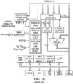
- Fig. 1 shows a block diagram of such a processing core. As can be seen, this core has typical digital signal processing capabilities such as an X Data RAM and a separate Y Data RAM and a DSP engine coupled with the RAMS and a register file such that the RAMs can be accessed both in parallel. Other typical elements of this processing core are shown. In addition this conventional DSP microcontroller shows in Fig.
- FIG. 1 shows registers of the core, such as the working registers of the register file and accumulator of the DSP engine as well as other typical DSP registers.
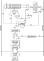
- Fig. 3 shows a more detailed block diagram of the DSP engine of the block diagram of Fig. 1 .
- the processing core as shown in Figs. 1-3 is a single processing core that comprises digital signal processing capabilities. It can be used in multi-core device as one of the cores.
- US Patent US 6,327,648 discloses a multiprocessor system for digital signal processing.
- Multi-processor core microcontrollers may be designed with entirely separated cores and each core may operate on a different system clock. Thus, to provide for the ability to communicate between the two or more cores, a specific communication interface is necessary. In particular, a means to move code protected data between processor memories on a multi-processor device is needed. Solution had to be fully configurable yet be efficient with regards to silicon use.
- an integrated circuit may comprise: a master processing core having a central processing unit coupled with a non-volatile memory; and a slave processing core operating independently from the master processing core and having a central processing unit coupled with volatile program memory; wherein the master central processing unit is configured to transfer program instructions into the non-volatile memory of the slave processing core; and wherein a transfer of said program instructions is performed by executing a dedicated instruction within the central processing unit of the master processing core.
- the dedicated instruction has a first operand defining a source address and a second operand defining a destination address, wherein the destination address is auto-incremented after execution of the instruction.
- the dedicated instruction causes an information word to be transferred into a buffer, and wherein the information is written into the volatile program memory from the buffer.
- the instruction causes the non-volatile memory to output said information whereupon said information is captured by said buffer.
- the information is a 24 bit word.
- the integrated circuit comprises a plurality of slave processing cores and the dedicated instruction has a third operand defining a target slave processing unit.
- the source address stored in the first operand can optionally be auto-incremented after execution of the instruction.
- the source address is a special function register of a peripheral device associated with the master processing core.
- the peripheral device is a serial communication peripheral.
- the peripheral device is a parallel input port.
- the master processing core is further operable to execute a further instruction that verifies an information stored in the non-volatile program memory.
- the further instruction causes a first information to be transferred into the buffer and wherein the content of the buffer is compared with a second information stored in the volatile memory.
- the further instruction comprises a first address which is applied to the non-volatile memory to output the first information and a second address which is applied to the volatile memory to output the second information.
- the further instruction further verifies error correcting code (ECC) associated with the first and second information.
- ECC error correcting code
- the ECC associated with the non-volatile memory can be read from the non-volatile memory and the ECC associated with the source is separately generated.
- the non-volatile memory of the first processing core comprises a code protection defined by a protection scheme and wherein the volatile program memory of the slave processing unit has a code protection that depends on a setting of the protection scheme.
- the protection scheme defines a plurality of segments of the non-volatile memory and wherein each segment has a protection setting in the protection scheme.
- each protection setting for the non-volatile memory has a setting for a read operation and a setting for a program or erase operation.
- the protection scheme provides for a predefined number of security levels, wherein each security level defines a protection setting for each segment.
- the code protection for the volatile program memory is the same as the code protection for one of the segments of the non-volatile memory.
- a register stores which segment of the non-volatile memory is selected to provide the code protection setting for the volatile memory.
- a setting for a read operation of the non-volatile memory applies to read and write operations of the volatile memory.
- when a segment is protected depending on a protection setting an instruction executed from one segment may not operate on a different segment.
- when a segment is protected, depending on a protection setting an read instruction executed from one segment may operate only on a predefined area of a different segment.
- the predefined area stores interrupt vectors.
- the non-volatile memory comprises a boot segment and a general segment.
- the non-volatile memory further comprises a test segment.
- a method for providing firmware for a processing core in a multi-core integrated circuit processing device comprising a first processing core having a first central processing unit coupled with a non-volatile memory and a second processing core operating independently from the first processing core and having a second central processing unit coupled with volatile program memory, may comprise: executing a dedicated instruction within the first central processing unit which causes data to be written into the non-volatile memory of the slave processing core.
- the dedicated instruction has a first operand defining a source address and a second operand defining a destination address, wherein the destination address is auto-incremented after execution of the instruction.
- an information word is transferred from the non-volatile memory into a buffer, and the information is written into the volatile program memory from the buffer.
- the method may further comprise repeating said dedicated instruction in a loop.
- the integrated circuit comprises a plurality of slave processing cores and the dedicated instruction has a third operand defining a target slave processing unit.
- the source address stored in the first operand can optionally be auto-incremented after execution of the instruction.
- the method may further comprise executing by the master processing core a further instruction that verifies an information stored in the non-volatile program memory.
- the further instruction causes a first information to be transferred into the buffer and wherein the content of the buffer is compared with a second information stored in the volatile memory.
- the further instruction comprises a first address which is applied to the non-volatile memory to output the first information and a second address which is applied to the volatile memory to output the second information.
- the further instruction further verifies error correcting code (ECC) associated with the first and second information.
- ECC error correcting code
- the ECC associated with the non-volatile memory can be read from the non-volatile memory and the ECC associated with the source is separately generated.
- the non-volatile memory of the first processing core comprises a code protection defined by a protection scheme and wherein the volatile program memory of the slave processing unit has a code protection that depends on a setting of the protection scheme.
- the protection scheme defines a plurality of segments of the non-volatile memory and wherein each segment has a protection setting in the protection scheme.
- each protection setting for the non-volatile memory has a setting for a read operation and a setting for a program or erase operation.
- the protection scheme provides for a predefined number of security levels, wherein each security level defines a protection setting for each segment.
- the code protection for the volatile program memory is the same as the code protection for one of the segments of the non-volatile memory.
- a register stores which segment of the non-volatile memory is selected to provide the code protection setting for the volatile memory.
- a setting for a read operation of the non-volatile memory applies to read and write operations of the volatile memory.
- a segment when a segment is protected, depending on a protection setting an instruction executed from one segment may not operate on a different segment.
- a protection setting an read instruction executed from one segment when a segment is protected, depending on a protection setting an read instruction executed from one segment may operate only on a predefined area of a different segment.
- the predefined area stores interrupt vectors.
- the non-volatile memory comprises a boot segment and a general segment. According to a further example, which does not form part of the invention, the non-volatile memory further comprises a test segment.
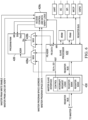
- a dual or multi core processing device 400 can be designed to have a master microcontroller 410 with a master central processing unit (CPU) 412 and one or slave units 420 each having a slave central processing unit 422 wherein a core design of each slave central processing unit 422 may be generally identical or similar to the core design of the master CPU 412.
- the slave CPU 422 may be different from the master CPU 412.
- the master microcontroller has its own set of peripheral devices as shown in Fig. 4 .
- a slave unit 420 may or may not have its own set of peripheral devices and, thus, form a microcontroller by itself.
- each master and slave device form more or less completely independent processing devices and may communicate with a dedicated bus or communication interface 430.
- Figs. 4 and 5 shows such a design with a master microcontroller 410 and a single slave microcontroller 420.
- a communication interface 430 is provided that allows for communication between the two cores 410, 420.
- Each processor 412, 422 may be designed in a Harvard architecture as shown. However, the principles according to the various embodiments may be easily translated into a von Neumann architecture.
- the master unit comprises, e.g., flash memory 416 used as the program memory and random access memory 414 used as data memory, each coupled with the master core 412.
- the slave unit 420 can be designed without flash memory. Instead a dedicated program random access memory 426 is provided. Due to the fact that this memory is volatile it will be loaded through the master 410 according to various embodiments. This design choice has the advantage that a bottleneck provided by flash technology is avoided. Flash memory is generally slower than RAM. Hence, there will be no read delays and the slave can be operated at a higher execution speed which may be very beneficial for certain high speed applications such as, e.g., SMPS applications. As stated above, more than one slave unit 420 may be implemented according to various embodiments. In case both cores are identical, the master core 412 can be designed to include additional instructions which may either not be implemented in the slave unit 422 or nonfunctional in the slave unit.
- additional instructions allow the transfer of data from the flash memory 416 or from an external source into the PRAM 426 of the slave device 420.
- multiple cores may be implemented within a single chip device and each core may have an assigned configuration register, wherein one of the bits of such a register may define whether the respective unit is a master or a slave.
- Logic may be present that allows for only one of the cores to be set as a master. Once this bit has been set, the additional instruction may be allowed to be executed. In the other units (slaves) these instructions may not be executed, for example, they could be interpreted as illegal opcodes.
- Control logic to access the PRAM 426 by the master unit 410 can be either located in the master unit as shown in Fig. 4 with buffer/comparator unit 418.
- a similar unit may be arranged within the slave unit 420 as shown in Figure 5 with PRAM wrapper unit 428.
- Either unit is designed to grant access of the PRAM either exclusively to the master unit 410 or to the slave unit 420.
- Other embodiments may place some part of the logic within the master core and other parts in the salve core or arrange the logic outside both units.
- communication interface 430 may be insider either unit or entirely outside both units. Additional control for the PRAM access units 418 or 428may be provided by the communication interface 430 as indicated in Fig. 5 with the dotted line.
- FIG. 5 also shows additional slave units 440 and 450 with dotted lines. All units may connect through a bus and associated wrapper units 428 in each slave unit.
- the embodiments are therefore not limited to a dual core implementation. A person skilled in the art will realize that other implementations are possible.
- Fig. 6 shows a block diagram of an exemplary interface at the slave side.
- the master slave interface forms the communication interface 430.
- Two multiplexers 428a, 428b grant access to the data and address bus of the program RAM 426, respectively.
- Additional access logic 428c is shown which is connected to the master unit 410, the slave core 422 and the PRAM 426.
- the communication interface 430 controls the multiplexers to give access to the master unit 410 while the slave processor is held in a reset state. Once the PRAM 426 has been loaded with the slave firmware, the multiplexers 428a, 428b will be controlled to grant access back to the slave unit 420 and the CPU 422 will be released from reset.
- the access control and data verify logic 428c may distribute the read and write and enable signals which may come either from the master unit 410 or the slave unit 420.
- the interface as shown in Fig. 6 may provide a write only path between the master unit 410 and the PRAM 426.
- the access control and data verify logic 428c may be configured to perform a verification of written data.
- the access control and data verify logic may operate in two different modes when coupled with the master unit 410. In a first mode, it provides the logic signals for writing the slave firmware into the PRAM 426, wherein data bytes are written in any suitable manner, for example, consecutively into the PRAM 426. In a second mode, the unit 428c may provide a verification function. Instead of writing the data transmitted, the unit 428c compares the data provided by the master unit 410 with the content of PRAM 426 to verify that it has been programmed correctly. Other embodiments of the master/slave interface with respect to the PRAM are possible.
- a Slave processor load/verify methodology for a multi-core device in particular a dual core microcontroller, can be provided.
- This provides an improved efficiency and performance with respect to conventional multi-core devices, especially for tight control loop applications (e.g. SMPS applications) using a DSP engine within the core.
- a processing core does not have to be designed to include a DSP engine.
- the principles according to various embodiments apply to a processing core which only includes a conventional CPU.
- the efficiency and performance of an associated C compiler will be improved by such an improved instruction set.
- a new dual-(multi-) core architecture includes dedicated CPU instructions to load & verify the Slave core Program RAM (PRAM).
- PRAM Program RAM
- a dual core device targets 100MHz for the Master unit 410 using Flash memory as its program memory (e.g., at 0.75 MIPs/MHz) and 120MHz for the Slave unit 420 using PRAM as its program memory (e.g., at 0.9 MIPs/MHz).
- the PRAM choice for program memory 426 in the slave unit 420 allows this unit to run more efficiently and at a higher speed.
- latency with hardware context switching for DSP may also need to be reduced.
- ISA improvements may be needed to improve DSP algorithm efficiency. Gains in compiler efficiency could be achieved with bit field instructions and a faster divider with a more flexible register utilization according to some embodiments.
- CPU improvements may comprise: Dual-core support instructions which provide for some or all of the following DSP improvements: Load & verify the Slave core Program RAM (PRAM); Hardware context switch extended to include DSP accumulators, status and DSP engine configuration; Data limit (bounds checking) instructions; Accumulator 32-bit data load/store instructions; and DSP normalization instruction.
- DSP improvements may comprise: Dual-core support instructions which provide for some or all of the following DSP improvements: Load & verify the Slave core Program RAM (PRAM); Hardware context switch extended to include DSP accumulators, status and DSP engine configuration; Data limit (bounds checking) instructions; Accumulator 32-bit data load/store instructions; and DSP normalization instruction.
- Compiler efficiency gains that can be achieved are: Bit field instructions and Divide instruction improvements.
- a dual core microcontroller with DSP functionality may comprise a Slave core with PRAM Load (LDSLV) & Verify (VFSLV) instructions added to facilitate Slave program initialization.
- LDSLV Slave core with PRAM Load
- VFSLV Verify
- These instructions are designed to be a faster alternative to moving data from a memory mapped image of the PRAM when compared to using conventional program space visibility (PSV) addressing or TBLWTx instructions.
- PSV program space visibility
- Another benefit of using unique instructions to load/verify the PRAM is that it simplifies the design and verification by not having to remap the PRAM into Master address space, and keeping the existing PSV CPU instruction flow (and just have the Slave snoop the passing address & data).
- an existing MOV instruction could be enhanced with a control flag to enable a Slave PRAM capture function.
- the LDSLV instruction differs from other data move instructions in so much as it can move an entire instruction word (I-word) from PS (Flash) to PS (Save PRAM) in 2 cycles. Each read will fetch a 24-bit word from Flash and then effect a write of that word into the target Slave PRAM.
- a conventional dsPIC/PIC24 CPU architecture has no means to move data values larger than 16-bits from Flash, so the data is not moved through the Master CPU but captured (when available on the Flash data bus) by the Slave.
- these new instructions are unique in that they are capable of moving data (as a single entity) that is wider than the natural data width of the processor that is executing them.
- the Slave will use the captured data to either write it to the specified PRAM address (LDSLV), or compare it with the contents of the specified PRAM address (VFSLV).
- LDSLVNFSLV instructions operate in an identical fashion except that VFSLV asserts signal cpu_slave_pram _verify_en to indicate that data read from the Master Flash is to be compared against the PRAM contents (instead of being loaded into the PRAM).
- These instructions may allow to transfer data from a predefined source including the flash memory 416 of the master device 410 into the program RAM (PRAM) 426.
- the master device 410 may provide for dedicated instructions to transfer and to verify transferred data. For example:
- Example 1 The code snippet shown in Example 1 demonstrates how the LDSLV instruction could be used during application initialization to load the PRAM of Slave #0.
- Example 2 The code snippet shown in Example 2 demonstrates how the VFSLV instruction could be used during application initialization to verify the PRAM contents of Slave #0.
- Example 3 The code snippet shown in Example 3 demonstrates how the LDSLV instruction could be used to block fill (i.e., load with a constant value) the PRAM of Slave #0.
- the constant is sourced from Flash using register indirect address for LDSLV (no post-increment).
- the block fill opcode value may be a variable sourced from the NVM Controller 24-bit NVMDATAL register.
- Any instruction opcode may be loaded into NVMDATAL and subsequently loaded into the PRAM.
- the VFSLV instruction may be used in the same manner to confirm the success of the LDSLV operation. This approach may also be used to load all or part of the PRAM with data sourced externally from the device, removing the need to first program it into the Master Flash memory as shown in Example 4.
- additional instructions may be implemented in a CPU with DSP engine.
- Such additional instructions do not necessarily require the implementation of the above mentioned load/verify instructions. Moreover, they do not require a multi core design but could also be implemented in a single core device comprising a CPU and integrated DSP engine.
- a first type of instruction may be a 16-bit data bounds check and limit functionality may add Force data Limit (FLIM/FLIM.v) instructions to accelerate 16-bit data bounds check and limit operations.
- FLIM/FLIM.v Force data Limit
- Such an instruction compares a target signed value with an upper and lower limit held in respective W registers. If the target value is greater than upper or less than lower limit, the exceeded limit register is loaded with the target signed value.
- a saturation function can be defined with user selectable upper and lower limits.
- a second additional instruction is an accumulator max and min instructions (MAXAB/MINAB) added to accelerate DSP accumulator based bounds check and limit operations: These instructions compare a signed value in the target accumulator with an upper (MAXAB) or lower (MINAB) limit held in the other accumulator. If the limit accumulator value is greater than upper (MAXAB) or less than lower (MINAB) limit, the limit accumulator is copied into the target accumulator.
- MAXAB/MINAB accumulator max and min instructions
- the minimum limit instruction may be designed to perform like a no-operation instruction if no limit is reached, thereby not affecting the flags of the status register.
- the branch instruction needs to be executed only once. If the maximum limit instruction triggers a flag, the minimum limit instruction would not reset it as it would execute like a nop instruction. The following branch instruction would execute correctly. This functionality may only require that the MAXAB(.v) instruction is executed before the MINAB(.v) instruction.
- LAC.d/SAC.d a 32-bit Load/Store Accumulator instructions
- LAC/SAC existing Load/Store Accumulator instructions move 16-bit data
- instructions extended to move 32-bit data may comprise:
- these can be implemented as single instruction words, which may execute in 2 cycles.
- an accumulator normalization (NORM) instruction can be added to accelerate existing normalization sequence (using FBCL instruction).
- FBCL Find First Bit Clear Left
- FBCL 6 instruction, 5 cycle operation (up to 16-bit shift only).
- Some embodiments may implement a NORM instruction that uses only 1 instruction word and executes in 1 cycle.
- the instruction automatically normalizes target accumulator by up to 16-bits in either direction. It may be cascaded for normalizations >16bits:
- NORM instruction may be able to normalize the entire accumulator in a single iteration.
- Bit field instructions are added to improve compiler efficiency. Compiled code frequently needs to insert or extract multiple bits within a target word: Bit field offsets and widths are invariably constant values
- bit field instructions are 2 word, 2 cycle operations: Without bit field, entire operation requires around 7 words, 7 cycles to complete; With bit field, entire operation requires around 4 words, 4 cycles to complete.
- a divide improvement provide an interruptible, non-restoring divide suite of instructions (same as for a conventional dsPIC): Execution time is now 7 cycles (P33E:19 cycles) for all divide instructions (includes 1 cycle for REPEAT instruction) and is fully backwards compatible with existing application code using original divide REPEAT count.
- an alternate set of divide instructions can be provided to improve compiler register allocation efficiency: Existing (32/16-bit) divide instructions: Dividend in Wm+1:Wm, Divisor in Wn, and Remainder:Quotient in W1 :W0
- LDSLV and VFSLV are specifically designed for multi-core devices, all other instructions may be optionally implemented in any combination:
- a code protect scheme for a dual-(multi-) core processor may be provided.
- This protection scheme is in particular beneficial for the Slave processor in a dual core microcontroller.
- this concept may also apply to a single core processor or microcontroller.
- Fig. 7 shows an exemplary code protect scheme 700. Flash memory may be split into several segments, each with its own rules pertaining to access of the other. For example, configuration registers which may be only configured during programming of the device or a fuse mechanism may be provided to set the access protection scheme.
- Fig. 7 shows that the flash is divided into a user flash and a test flash partition. However, other embodiments may only provide a single partition or even more partitions.
- the user flash partition is segmented into a boot segment and a general segment.
- smaller segments for interrupt vector tables IVT and AIVT may be provided, which may be included into the boot segment or which may have a separate protection depending on the currently set protection level.
- Fig. 7 shows an interrupt vector table IVT and an alternate interrupt vector table AIVT at different location.
- other embodiments may integrate these two table into one segment VS that may be located before the boot segment BS or at any other suitable location.
- a configuration segment may be provided that comprises various device configuration registers that can only be written when the device is programmed, for example, by the integrated in-circuit program functions.
- the arrangement of the segments may differ according to a respective implementation.
- the protection scheme allows for a variety of different settings wherein the each segment may be protected differently. In particular, access from one segment to another segment may be restricted according to a specific setting. Furthermore, vectoring into a segment may be restricted according to a security setting.
- the Test address space contains a few special sectors of Flash, all in the upper (highest address) half of the Program Space, which may for example be a 24-bit Program Space.
- the Configuration segment in such an embodiment (typically a single sector or less) resides within User Flash address space (lower half of the 24-bit Program Space:
- Flash Controller All "fuse" data is automatically read and loaded into special device configuration registers by the Flash Controller as a part of the device reset sequence.
- each segment may have its own access rules to prevent read/write access from another segment (hereinafter designated as "outside" access).
- vectoring into a segment may be restricted, in particular in a high security setting.
- a table may define the settings for each segment depending on what type of operation is performed wherein different operations may have different security settings as will be shown in more detail in Fig. 10 .
- the security can be split into read and write/erase protection separately, wherein, for example, a write protection bit may be used to set the write protection separately.
- the implementation may vary according to various embodiments.
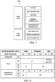
- Fig. 8 shows an embodiment with three different levels of protection for the boot segment.
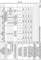
- Fig. 10 shows an embodiment with three different levels of protection for the general segment. Similar tables may be used for the other segments.
- Each protection level provides separate protection for a read access to different segments from outside the segment.
- each level may set whether write protection is set or not.
- a first level provides no read protection which generally applies to all accessed segments. If a write protection is active in this mode, it will be applied to all segments which then cannot be programmed or erased from "outside" the respective segment.
- FIG. 8 shows the protection for the boot segment. In this setting, the boot segment cannot be read or written to from "outside" and depending on the write protection setting, may not be written to from actions executed within the boot segment.
- Fig. 10 shows the setting for the general segment.
- the boot segment as well as the general segment can perform read operations within the general segment. Writing to the general segment is only allowed if the write protect bit is not set. Any operation from within the test segment will not allow read or write access to the general segment.
- the third level is shown as the high protection level.
- this additional protection may prevent any modifications of the vector table.
- the protection may be identical to the standard setting.
- Fig. 10 shows for the high security setting for the general segment, that any access from the outside is prohibited.
- the general segment can only be accessed from within the general segment. Even a Write access from within the general segment GS may be prohibited by setting the respective protection bit.
- Fig. 11 shows an example with a more detailed table with the security operations in application mode according to another example in more detail.
- the operations are listed under the left-most column, and the corresponding influence on GS, BS, CS and VS is shown in the corresponding row.
- Various operations are defined.
- the first line (PC Rollover into Segment) concerns a program counter roll-over into another segment.
- the second line (PFC to Segment) concerns any type of program flow change, such as execution of a jump or a branch instruction and its effect on the various segments.
- the next line (Vector from IVT or AIVT) concerns vectoring into a specific segment.
- the next line (Table Read/PSV) concerns PSV or table read instruction access to a segment.
- the next line concerns a page erase function that would affect a respective segment.
- the next line (Row Program) concerns the programming of a memory row.
- Other actions are sown in the following rows.
- different protection settings may apply to different types of action.
- Certain actions such as read and write operations may be performed within one segment but affect other segments.
- the protection scheme according to various embodiments allows to selectively protect these actions.
- Some actions such as those caused by an interrupt may not per se come from a specific segment, and therefore the table in Fig. 11 does not distinguish between the segments from they are executed.
- the table in Fig. 11 shows whether the action is allowed by showing an "OK" in the respective table cell or prohibited by showing either a "No" or "0's", wherein the latter indicates that the operation will produce a "0" read.
- Fig. 11 shows that for the configuration segment CS an additional security level may be implemented that may allow a separate intermediate protection level.
- the Slave PRAM 426 may be allocated to either the boot segment (BS) or the general segment (GS) address space, for example, by a fuse circuit of by configuration registers as mentioned above. According to another embodiment, the Slave PRAM can only inherit Master segment GS security.
- the Slave PRAM 426 will assume the security level assigned to the corresponding Master Flash segment of flash memory 416.
- the LDSLV/VFSLV instruction execution is now implemented such that it is sensitive to the respective Flash execution segment from which it is executed and to which the respective PRAM segment is assigned.
- the associated code protect security levels are applied when such an instruction is executed.
- the LDSLV/VFSLV are therefore seen within the PRAM as a read function.
- the program or page erase function and its associated security rules only applies to the flash memory.
- the already defined rules for BS/GS read of the Flash memory 416 will also be applied to Slave PRAM access when using the LDSLV/VFSLV instructions, which perform a read or write in the PRAM, such that:
- LDSLV/VFSLV execution will have no effect. Also, according to other embodiments other conditions may apply. The above conditions are mere examples. It is assumed that the Flash access code protect rules (for the source data read) will be met.
- Fig. 9 shows an extended code protect scheme for the boot segment similar to that shown in Fig. 8 . Again similar tables may be used for other segments. If the PRAM 426 is assigned to the boot segment of the master Flash memory 416, it may therefore be protected from untrusted code in segment GS by setting Master BS to any security level (i.e., a level other than 'None'). Conversely, if the PRAM is assigned to the segment GS of the master, it may also be protected from untrusted code in BS by setting Master GS to 'High' security.
Landscapes
- Engineering & Computer Science (AREA)
- Theoretical Computer Science (AREA)
- Software Systems (AREA)
- General Engineering & Computer Science (AREA)
- Physics & Mathematics (AREA)
- General Physics & Mathematics (AREA)
- Computer Hardware Design (AREA)
- Computer Security & Cryptography (AREA)
- Executing Machine-Instructions (AREA)
- Storage Device Security (AREA)
- Advance Control (AREA)
Claims (15)
- Integrierte Schaltung, die aufweist:einen Master-Verarbeitungskern, der eine zentrale Verarbeitungseinheit (412) aufweist, die mit einem nichtflüchtigen Speicher (416) gekoppelt ist;einen Slave-Verarbeitungskern, der unabhängig von dem Master-Verarbeitungskern arbeitet und eine zentrale Verarbeitungseinheit (422) aufweist, die mit einem flüchtigen Programmspeicher (426) gekoppelt ist;wobei die Master-Zentraleinheit (412) ausgebildet ist, eine Übertragung von Programmanweisungen in den flüchtigen Speicher (426) des Slave-Verarbeitungskerns zu bewirken;wobei eine Programmanweisung für den Slave-Verarbeitungskern breiter ist als eine Datenbreite des Master-Verarbeitungskerns; undwobei eine Übertragung der Programmanweisungen nur durch Ausführen einer dedizierten Anweisung (LDSLV) innerhalb der zentralen Verarbeitungseinheit (412) des Master-Verarbeitungskerns durchgeführt werden kann, wobei die Übertragung durch Logik (428) oder durch einen Puffer ( 418/428) stattfindet und damit ausgeführt wird, ohne die Programmanweisungen durch den Master-Verarbeitungskern zu bewegen.
- Verfahren zum Bereitstellen von Firmware für einen Verarbeitungskern in einer integrierten Mehrkemschaltungs-Verarbeitungsvorrichtung (400; 500), die einen Master-Verarbeitungskern aufweist, der eine erste zentrale Verarbeitungseinheit (412) aufweist, die mit einem nichtflüchtigen Speicher (416) gekoppelt ist, und einen Slave-Verarbeitungskern aufweist, der unabhängig von dem Master-Verarbeitungskern arbeitet und eine zweite zentrale Verarbeitungseinheit (422) aufweist, die mit einem flüchtigen Programmspeicher (426) gekoppelt ist, wobei eine Programmanweisung für den Slave-Verarbeitungskern breiter ist als eine Datenbreite des Master-Verarbeitungskerns ;
wobei das Verfahren aufweist:
Ausführen einer dedizierten Anweisung (LDSLV) innerhalb der ersten zentralen Verarbeitungseinheit (412), die bewirkt, dass Daten in den flüchtigen Programmspeicher (426) des Slave-Verarbeitungskerns geschrieben werden, wobei die Übertragung durch Logik (428) oder durch einen Puffer (418/428) stattfindet und damit ausgeführt wird, ohne die Programmbefehle durch den Master-Verarbeitungskern zu bewegen. - Integrierte Schaltung nach Anspruch 1 oder Verfahren nach Anspruch 2, wobei der dedizierte Befehl (LDSLV) einen ersten Operanden aufweist, der eine Quelladresse definiert, und einen zweiten Operanden aufweist, der eine Zieladresse definiert, wobei die Zieladresse nach Ausführung der Anweisung automatisch inkrementiert wird.
- Integrierte Schaltung oder Verfahren nach einem der vorhergehenden Ansprüche, wobei die dedizierten Befehle (LDSLV) ausgebildet sind, ein Befehlswort in zwei Zyklen zu bewegen.
- Integrierte Schaltung oder Verfahren nach einem der vorhergehenden Ansprüche, wobei der flüchtige Speicher (426) des Slave-Verarbeitungskems zumindest zwei Panels aufweist, wobei nur ein Panel in Bezug auf den Slave-Verarbeitungskern aktiv ist und wobei der Master-Verarbeitungskern so ausgebildet ist, dass er Programmanweisungen nur in ein inaktives Panel überträgt.
- Integrierte Schaltung oder Verfahren nach einem der vorhergehenden Ansprüche, wobei der dedizierte Befehl (LDSLV) bewirkt, dass ein Informationswort, vorzugsweise ein 24-Bit-Wort, in einen Puffer (418; 428) übertragen wird, und wobei das Informationswort aus dem Puffer (418; 428) in den flüchtigen Programmspeicher (426) geschrieben wird.
- Integrierte Schaltung oder Verfahren nach Anspruch 6, wobei die Anweisung (LDSLV) bewirkt, dass der nichtflüchtige Speicher (416) das Informationswort ausgibt, woraufhin das Informationswort durch den Puffer (418; 428) erfasst wird.
- Integrierte Schaltung oder Verfahren nach einem der vorhergehenden Ansprüche, wobei die integrierte Schaltung (500) mehrere Slave-Verarbeitungskerne (420, 440, 450) aufweist und die dedizierte Anweisung (LDSLV) einen dritten Operanden aufweist, der eine Ziel-Slave-Verarbeitungseinheit (422) definiert.
- Integrierte Schaltung oder Verfahren nach einem der Ansprüche 3 bis 8, wobei die im ersten Operanden gespeicherte Quelladresse optional nach Ausführung des Befehls automatisch inkrementiert werden kann.
- Integrierte Schaltung oder Verfahren nach einem der Ansprüche 3 bis 9, wobei die Quelladresse in einem speziellen Funktionsregister einer Peripherievorrichtung, vorzugsweise einer seriellen Kommunikationsperipherie oder einem parallelen Ein-/Ausgangsport gespeichert ist, der dem Master-Verarbeitungskern (412) zugeordnet ist.
- Integrierte Schaltung oder Verfahren nach einem der vorhergehenden Ansprüche, wobei der Master-Verarbeitungskern (412) weiterhin betreibbar ist, um eine weitere Anweisung (VFSLV) auszuführen, die ein im flüchtigen Programmspeicher (426) gespeichertes Informationswort verifiziert.
- Integrierte Schaltung oder Verfahren nach Anspruch 11, wobei die weitere Anweisung (VFSLV) bewirkt, dass ein erstes Informationswort in den Puffer (418; 428) übertragen wird, und wobei der Inhalt des Puffers (418; 428) mit einem zweiten Informationswort verglichen wird, das in dem flüchtigen Speicher (426) gespeichert ist.
- Integrierte Schaltung oder Verfahren nach Anspruch 11 oder Anspruch 12, wobei die weitere Anweisung (VFSLV) eine erste Adresse aufweist, die auf den nichtflüchtigen Speicher (416) angewendet wird, um die erste Information auszugeben, und eine zweite Adresse aufweist, die auf den flüchtigen Speicher (426) angewendet wird, um die zweite Information auszugeben.
- Integrierte Schaltung nach einem der Ansprüche 11 bis 13, wobei die weitere Anweisung (VFSLV) weiterhin den dem ersten und zweiten Informationswort zugeordneten Fehlerkorrekturcode (ECC) verifiziert, wobei der dem flüchtigen Speicher (426) zugeordnete ECC aus dem flüchtigen Speicher (426) gelesen werden kann und der der Quelle (416) zugeordnete ECC separat erzeugt wird.
- Integrierte Schaltung oder Verfahren nach einem der vorhergehenden Ansprüche, wobei der nichtflüchtige Speicher (416) des ersten Verarbeitungskerns einen Codeschutz aufweist, der durch ein Schutzschema definiert ist, und wobei der flüchtige Programmspeicher (426) der Slave-Verarbeitungseinheit einen Codeschutz aufweist, der von einer Einstellung des Schutzschemas abhängig ist.
Applications Claiming Priority (3)
| Application Number | Priority Date | Filing Date | Title |
|---|---|---|---|
| US201562154927P | 2015-04-30 | 2015-04-30 | |
| US201562195692P | 2015-07-22 | 2015-07-22 | |
| PCT/US2016/030159 WO2016176593A1 (en) | 2015-04-30 | 2016-04-29 | Central processing unit with enhanced instruction set |
Publications (2)
| Publication Number | Publication Date |
|---|---|
| EP3289442A1 EP3289442A1 (de) | 2018-03-07 |
| EP3289442B1 true EP3289442B1 (de) | 2023-04-19 |
Family
ID=55963480
Family Applications (1)
| Application Number | Title | Priority Date | Filing Date |
|---|---|---|---|
| EP16722012.8A Active EP3289442B1 (de) | 2015-04-30 | 2016-04-29 | Zentrale prozessoreinheit mit verbessertem befehlssatz |
Country Status (7)
| Country | Link |
|---|---|
| US (2) | US10983931B2 (de) |
| EP (1) | EP3289442B1 (de) |
| JP (1) | JP2018514868A (de) |
| KR (1) | KR20170140225A (de) |
| CN (1) | CN107548492B (de) |
| TW (1) | TW201706856A (de) |
| WO (1) | WO2016176593A1 (de) |
Families Citing this family (9)
| Publication number | Priority date | Publication date | Assignee | Title |
|---|---|---|---|---|
| US10019314B2 (en) | 2016-04-27 | 2018-07-10 | Silicon Motion Inc. | Flash memory apparatus and storage management method for flash memory |
| CN111679787B (zh) | 2016-04-27 | 2023-07-18 | 慧荣科技股份有限公司 | 闪存装置、闪存控制器及闪存存储管理方法 |
| US11872623B2 (en) | 2016-11-04 | 2024-01-16 | Lg Chem, Ltd. | Thermosetting composition |
| DE112018000842T5 (de) * | 2017-06-12 | 2019-12-24 | Sandisk Technologies Llc | Mehrkern-on-die-speichermikrocontroller |
| KR102032146B1 (ko) | 2018-04-11 | 2019-10-15 | 경희대학교 산학협력단 | 소자 결점을 보완하기 위한 구간 선형 정류 유닛을 사용하는 인공신경망 시스템 |
| CN111382429B (zh) * | 2018-12-27 | 2022-12-27 | 华为技术有限公司 | 指令的执行方法、装置及存储介质 |
| CN109886416A (zh) * | 2019-02-01 | 2019-06-14 | 京微齐力(北京)科技有限公司 | 集成人工智能模块的系统芯片及机器学习方法 |
| CN109870921B (zh) * | 2019-03-26 | 2022-04-01 | 广东美的制冷设备有限公司 | 驱动控制电路与家电设备 |
| TWI715371B (zh) | 2019-12-25 | 2021-01-01 | 新唐科技股份有限公司 | 一次性可編程記憶體裝置及其容錯方法 |
Family Cites Families (29)
| Publication number | Priority date | Publication date | Assignee | Title |
|---|---|---|---|---|
| US5167028A (en) * | 1989-11-13 | 1992-11-24 | Lucid Corporation | System for controlling task operation of slave processor by switching access to shared memory banks by master processor |
| US5226138A (en) * | 1990-11-27 | 1993-07-06 | Sun Microsystems, Inc. | Method for selectively transferring data instructions to a cache memory |
| US6327648B1 (en) * | 1994-12-09 | 2001-12-04 | Cirrus Logic, Inc. | Multiprocessor system for digital signal processing |
| US7272703B2 (en) * | 1997-08-01 | 2007-09-18 | Micron Technology, Inc. | Program controlled embedded-DRAM-DSP architecture and methods |
| ITMI981564A1 (it) * | 1998-07-09 | 2000-01-09 | St Microelectronics Srl | Memoria non volatile in grado di eseguire un programma autonomamente |
| US6260082B1 (en) * | 1998-12-23 | 2001-07-10 | Bops, Inc. | Methods and apparatus for providing data transfer control |
| GB2365545B (en) * | 1999-12-23 | 2004-06-02 | Ibm | Data processing system with master and slave processors |
| US6691216B2 (en) | 2000-11-08 | 2004-02-10 | Texas Instruments Incorporated | Shared program memory for use in multicore DSP devices |
| US6895479B2 (en) * | 2000-11-15 | 2005-05-17 | Texas Instruments Incorporated | Multicore DSP device having shared program memory with conditional write protection |
| JP2002185430A (ja) * | 2000-12-13 | 2002-06-28 | Sony Corp | 受信装置及び方法 |
| US6349056B1 (en) | 2000-12-28 | 2002-02-19 | Sandisk Corporation | Method and structure for efficient data verification operation for non-volatile memories |
| US7007172B2 (en) * | 2001-06-01 | 2006-02-28 | Microchip Technology Incorporated | Modified Harvard architecture processor having data memory space mapped to program memory space with erroneous execution protection |
| US7571287B2 (en) * | 2003-03-13 | 2009-08-04 | Marvell World Trade Ltd. | Multiport memory architecture, devices and systems including the same, and methods of using the same |
| CN1301473C (zh) | 2003-09-17 | 2007-02-21 | 中兴通讯股份有限公司 | 多处理器系统共享引导模块的方法 |
| US7325122B2 (en) * | 2004-02-20 | 2008-01-29 | International Business Machines Corporation | Facilitating inter-DSP data communications |
| JP4575059B2 (ja) * | 2004-07-21 | 2010-11-04 | 株式会社日立製作所 | ストレージ装置 |
| US7917753B2 (en) * | 2005-05-16 | 2011-03-29 | Texas Instruments Incorporated | Transferring control between programs of different security levels |
| CN101366004A (zh) | 2005-12-06 | 2009-02-11 | 波士顿电路公司 | 用于带有专用线程管理的多核处理的方法和设备 |
| US20080235493A1 (en) * | 2007-03-23 | 2008-09-25 | Qualcomm Incorporated | Instruction communication techniques for multi-processor system |
| WO2008155812A1 (ja) * | 2007-06-18 | 2008-12-24 | Fujitsu Limited | プロセッサおよびプリフェッチ支援プログラム |
| US8650440B2 (en) * | 2008-01-16 | 2014-02-11 | Freescale Semiconductor, Inc. | Processor based system having ECC based check and access validation information means |
| US20110087922A1 (en) * | 2009-10-09 | 2011-04-14 | National Tsing Hua University | Test method and tool for master-slave systems on multicore processors |
| US8478974B2 (en) | 2010-06-23 | 2013-07-02 | Assured Information Security, Inc. | Method and system for reducing an impact of malware during a booting sequence |
| US8904190B2 (en) | 2010-10-20 | 2014-12-02 | Advanced Micro Devices, Inc. | Method and apparatus including architecture for protecting sensitive code and data |
| US9021170B2 (en) * | 2011-06-29 | 2015-04-28 | Texas Instruments Incorporated | System and method for improving ECC enabled memory timing |
| US9195581B2 (en) * | 2011-07-01 | 2015-11-24 | Apple Inc. | Techniques for moving data between memory types |
| GB2513727B (en) | 2012-06-27 | 2015-06-24 | Nordic Semiconductor Asa | Memory protection |
| US9858229B2 (en) | 2014-09-30 | 2018-01-02 | International Business Machines Corporation | Data access protection for computer systems |
| RU2580016C1 (ru) * | 2014-10-17 | 2016-04-10 | Закрытое акционерное общество "Лаборатория Касперского" | Способ передачи управления между областями памяти |
-
2016
- 2016-04-29 JP JP2017554326A patent/JP2018514868A/ja active Pending
- 2016-04-29 EP EP16722012.8A patent/EP3289442B1/de active Active
- 2016-04-29 US US15/141,823 patent/US10983931B2/en active Active
- 2016-04-29 CN CN201680024293.4A patent/CN107548492B/zh active Active
- 2016-04-29 KR KR1020177030823A patent/KR20170140225A/ko unknown
- 2016-04-29 WO PCT/US2016/030159 patent/WO2016176593A1/en unknown
- 2016-05-02 TW TW105113680A patent/TW201706856A/zh unknown
-
2019
- 2019-01-17 US US16/250,274 patent/US10776292B2/en active Active
Also Published As
| Publication number | Publication date |
|---|---|
| CN107548492B (zh) | 2021-10-01 |
| CN107548492A (zh) | 2018-01-05 |
| KR20170140225A (ko) | 2017-12-20 |
| JP2018514868A (ja) | 2018-06-07 |
| WO2016176593A1 (en) | 2016-11-03 |
| US10776292B2 (en) | 2020-09-15 |
| EP3289442A1 (de) | 2018-03-07 |
| US10983931B2 (en) | 2021-04-20 |
| US20160321202A1 (en) | 2016-11-03 |
| TW201706856A (zh) | 2017-02-16 |
| US20190188163A1 (en) | 2019-06-20 |
Similar Documents
| Publication | Publication Date | Title |
|---|---|---|
| US10776292B2 (en) | Apparatus and method for protecting program memory for processing cores in a multi-core integrated circuit | |
| US10360162B2 (en) | Processing systems and methods for transitioning between privilege states based on an address of a next instruction to be fetched | |
| US9733950B2 (en) | Boot sequencing for multi boot devices | |
| US11048588B2 (en) | Monitoring the operation of a processor | |
| GB2514882A (en) | Instruction emulation processors, methods, and systems | |
| KR101780303B1 (ko) | 시스템 호출을 위한 강건하고 높은 성능의 명령어들 | |
| US11580226B2 (en) | Hybrid firmware code protection | |
| KR20100101090A (ko) | 개선된 마이크로프로세서 또는 마이크로컨트롤러 | |
| US20140281473A1 (en) | Minimizing Switchover Time In A Hot Swappable Program Memory | |
| KR20060002664A (ko) | 내장 시스템의 메모리 어드레스의 매핑을 제어하는 장치와방법 | |
| BR102020019663A2 (pt) | algoritmo de remoção de linha de cache à base de prioridade de tecnologia de alocação de cache flexível | |
| TWI617984B (zh) | 雙開機區段切換機制 | |
| KR20100087309A (ko) | 개선된 마이크로프로세서 또는 마이크로컨트롤러 | |
| TWI467475B (zh) | 無關於特權位準的區段暫存器讀與寫的系統、設備及方法 | |
| US20220382550A1 (en) | Method and apparatus for efficient programmable instructions in computer systems | |
| US9405534B2 (en) | Compound complex instruction set computer (CCISC) processor architecture | |
| US20020004877A1 (en) | Method and system for updating user memory in emulator systems | |
| JP4236808B2 (ja) | 不揮発メモリ内蔵マイクロコンピュータとその不揮発メモリの自己書換方法 | |
| KR20090128672A (ko) | 다중 부팅 모드를 지원하는 장치 및 방법 |
Legal Events
| Date | Code | Title | Description |
|---|---|---|---|
| STAA | Information on the status of an ep patent application or granted ep patent |
Free format text: STATUS: THE INTERNATIONAL PUBLICATION HAS BEEN MADE |
|
| PUAI | Public reference made under article 153(3) epc to a published international application that has entered the european phase |
Free format text: ORIGINAL CODE: 0009012 |
|
| STAA | Information on the status of an ep patent application or granted ep patent |
Free format text: STATUS: REQUEST FOR EXAMINATION WAS MADE |
|
| 17P | Request for examination filed |
Effective date: 20171128 |
|
| AK | Designated contracting states |
Kind code of ref document: A1 Designated state(s): AL AT BE BG CH CY CZ DE DK EE ES FI FR GB GR HR HU IE IS IT LI LT LU LV MC MK MT NL NO PL PT RO RS SE SI SK SM TR |
|
| AX | Request for extension of the european patent |
Extension state: BA ME |
|
| DAV | Request for validation of the european patent (deleted) | ||
| DAX | Request for extension of the european patent (deleted) | ||
| STAA | Information on the status of an ep patent application or granted ep patent |
Free format text: STATUS: EXAMINATION IS IN PROGRESS |
|
| 17Q | First examination report despatched |
Effective date: 20200429 |
|
| STAA | Information on the status of an ep patent application or granted ep patent |
Free format text: STATUS: EXAMINATION IS IN PROGRESS |
|
| STAA | Information on the status of an ep patent application or granted ep patent |
Free format text: STATUS: EXAMINATION IS IN PROGRESS |
|
| GRAP | Despatch of communication of intention to grant a patent |
Free format text: ORIGINAL CODE: EPIDOSNIGR1 |
|
| STAA | Information on the status of an ep patent application or granted ep patent |
Free format text: STATUS: GRANT OF PATENT IS INTENDED |
|
| INTG | Intention to grant announced |
Effective date: 20221110 |
|
| GRAS | Grant fee paid |
Free format text: ORIGINAL CODE: EPIDOSNIGR3 |
|
| GRAA | (expected) grant |
Free format text: ORIGINAL CODE: 0009210 |
|
| STAA | Information on the status of an ep patent application or granted ep patent |
Free format text: STATUS: THE PATENT HAS BEEN GRANTED |
|
| AK | Designated contracting states |
Kind code of ref document: B1 Designated state(s): AL AT BE BG CH CY CZ DE DK EE ES FI FR GB GR HR HU IE IS IT LI LT LU LV MC MK MT NL NO PL PT RO RS SE SI SK SM TR |
|
| REG | Reference to a national code |
Ref country code: GB Ref legal event code: FG4D |
|
| REG | Reference to a national code |
Ref country code: DE Ref legal event code: R096 Ref document number: 602016078884 Country of ref document: DE |
|
| REG | Reference to a national code |
Ref country code: CH Ref legal event code: EP |
|
| REG | Reference to a national code |
Ref country code: IE Ref legal event code: FG4D |
|
| REG | Reference to a national code |
Ref country code: AT Ref legal event code: REF Ref document number: 1561708 Country of ref document: AT Kind code of ref document: T Effective date: 20230515 |
|
| PGFP | Annual fee paid to national office [announced via postgrant information from national office to epo] |
Ref country code: DE Payment date: 20230523 Year of fee payment: 8 |
|
| REG | Reference to a national code |
Ref country code: LT Ref legal event code: MG9D |
|
| REG | Reference to a national code |
Ref country code: NL Ref legal event code: MP Effective date: 20230419 |
|
| REG | Reference to a national code |
Ref country code: AT Ref legal event code: MK05 Ref document number: 1561708 Country of ref document: AT Kind code of ref document: T Effective date: 20230419 |
|
| PG25 | Lapsed in a contracting state [announced via postgrant information from national office to epo] |
Ref country code: NL Free format text: LAPSE BECAUSE OF FAILURE TO SUBMIT A TRANSLATION OF THE DESCRIPTION OR TO PAY THE FEE WITHIN THE PRESCRIBED TIME-LIMIT Effective date: 20230419 |
|
| PG25 | Lapsed in a contracting state [announced via postgrant information from national office to epo] |
Ref country code: SE Free format text: LAPSE BECAUSE OF FAILURE TO SUBMIT A TRANSLATION OF THE DESCRIPTION OR TO PAY THE FEE WITHIN THE PRESCRIBED TIME-LIMIT Effective date: 20230419 Ref country code: PT Free format text: LAPSE BECAUSE OF FAILURE TO SUBMIT A TRANSLATION OF THE DESCRIPTION OR TO PAY THE FEE WITHIN THE PRESCRIBED TIME-LIMIT Effective date: 20230821 Ref country code: NO Free format text: LAPSE BECAUSE OF FAILURE TO SUBMIT A TRANSLATION OF THE DESCRIPTION OR TO PAY THE FEE WITHIN THE PRESCRIBED TIME-LIMIT Effective date: 20230719 Ref country code: ES Free format text: LAPSE BECAUSE OF FAILURE TO SUBMIT A TRANSLATION OF THE DESCRIPTION OR TO PAY THE FEE WITHIN THE PRESCRIBED TIME-LIMIT Effective date: 20230419 Ref country code: AT Free format text: LAPSE BECAUSE OF FAILURE TO SUBMIT A TRANSLATION OF THE DESCRIPTION OR TO PAY THE FEE WITHIN THE PRESCRIBED TIME-LIMIT Effective date: 20230419 |
|
| PG25 | Lapsed in a contracting state [announced via postgrant information from national office to epo] |
Ref country code: RS Free format text: LAPSE BECAUSE OF FAILURE TO SUBMIT A TRANSLATION OF THE DESCRIPTION OR TO PAY THE FEE WITHIN THE PRESCRIBED TIME-LIMIT Effective date: 20230419 Ref country code: PL Free format text: LAPSE BECAUSE OF FAILURE TO SUBMIT A TRANSLATION OF THE DESCRIPTION OR TO PAY THE FEE WITHIN THE PRESCRIBED TIME-LIMIT Effective date: 20230419 Ref country code: LV Free format text: LAPSE BECAUSE OF FAILURE TO SUBMIT A TRANSLATION OF THE DESCRIPTION OR TO PAY THE FEE WITHIN THE PRESCRIBED TIME-LIMIT Effective date: 20230419 Ref country code: LT Free format text: LAPSE BECAUSE OF FAILURE TO SUBMIT A TRANSLATION OF THE DESCRIPTION OR TO PAY THE FEE WITHIN THE PRESCRIBED TIME-LIMIT Effective date: 20230419 Ref country code: IS Free format text: LAPSE BECAUSE OF FAILURE TO SUBMIT A TRANSLATION OF THE DESCRIPTION OR TO PAY THE FEE WITHIN THE PRESCRIBED TIME-LIMIT Effective date: 20230819 Ref country code: HR Free format text: LAPSE BECAUSE OF FAILURE TO SUBMIT A TRANSLATION OF THE DESCRIPTION OR TO PAY THE FEE WITHIN THE PRESCRIBED TIME-LIMIT Effective date: 20230419 Ref country code: GR Free format text: LAPSE BECAUSE OF FAILURE TO SUBMIT A TRANSLATION OF THE DESCRIPTION OR TO PAY THE FEE WITHIN THE PRESCRIBED TIME-LIMIT Effective date: 20230720 Ref country code: AL Free format text: LAPSE BECAUSE OF FAILURE TO SUBMIT A TRANSLATION OF THE DESCRIPTION OR TO PAY THE FEE WITHIN THE PRESCRIBED TIME-LIMIT Effective date: 20230419 |
|
| REG | Reference to a national code |
Ref country code: CH Ref legal event code: PL |
|
| PG25 | Lapsed in a contracting state [announced via postgrant information from national office to epo] |
Ref country code: LU Free format text: LAPSE BECAUSE OF NON-PAYMENT OF DUE FEES Effective date: 20230429 Ref country code: FI Free format text: LAPSE BECAUSE OF FAILURE TO SUBMIT A TRANSLATION OF THE DESCRIPTION OR TO PAY THE FEE WITHIN THE PRESCRIBED TIME-LIMIT Effective date: 20230419 |
|
| REG | Reference to a national code |
Ref country code: BE Ref legal event code: MM Effective date: 20230430 |
|
| PG25 | Lapsed in a contracting state [announced via postgrant information from national office to epo] |
Ref country code: SK Free format text: LAPSE BECAUSE OF FAILURE TO SUBMIT A TRANSLATION OF THE DESCRIPTION OR TO PAY THE FEE WITHIN THE PRESCRIBED TIME-LIMIT Effective date: 20230419 |
|
| PG25 | Lapsed in a contracting state [announced via postgrant information from national office to epo] |
Ref country code: MC Free format text: LAPSE BECAUSE OF FAILURE TO SUBMIT A TRANSLATION OF THE DESCRIPTION OR TO PAY THE FEE WITHIN THE PRESCRIBED TIME-LIMIT Effective date: 20230419 |
|
| REG | Reference to a national code |
Ref country code: DE Ref legal event code: R097 Ref document number: 602016078884 Country of ref document: DE |
|
| PG25 | Lapsed in a contracting state [announced via postgrant information from national office to epo] |
Ref country code: SM Free format text: LAPSE BECAUSE OF FAILURE TO SUBMIT A TRANSLATION OF THE DESCRIPTION OR TO PAY THE FEE WITHIN THE PRESCRIBED TIME-LIMIT Effective date: 20230419 Ref country code: SK Free format text: LAPSE BECAUSE OF FAILURE TO SUBMIT A TRANSLATION OF THE DESCRIPTION OR TO PAY THE FEE WITHIN THE PRESCRIBED TIME-LIMIT Effective date: 20230419 Ref country code: RO Free format text: LAPSE BECAUSE OF FAILURE TO SUBMIT A TRANSLATION OF THE DESCRIPTION OR TO PAY THE FEE WITHIN THE PRESCRIBED TIME-LIMIT Effective date: 20230419 Ref country code: MC Free format text: LAPSE BECAUSE OF FAILURE TO SUBMIT A TRANSLATION OF THE DESCRIPTION OR TO PAY THE FEE WITHIN THE PRESCRIBED TIME-LIMIT Effective date: 20230419 Ref country code: LI Free format text: LAPSE BECAUSE OF NON-PAYMENT OF DUE FEES Effective date: 20230430 Ref country code: EE Free format text: LAPSE BECAUSE OF FAILURE TO SUBMIT A TRANSLATION OF THE DESCRIPTION OR TO PAY THE FEE WITHIN THE PRESCRIBED TIME-LIMIT Effective date: 20230419 Ref country code: DK Free format text: LAPSE BECAUSE OF FAILURE TO SUBMIT A TRANSLATION OF THE DESCRIPTION OR TO PAY THE FEE WITHIN THE PRESCRIBED TIME-LIMIT Effective date: 20230419 Ref country code: CZ Free format text: LAPSE BECAUSE OF FAILURE TO SUBMIT A TRANSLATION OF THE DESCRIPTION OR TO PAY THE FEE WITHIN THE PRESCRIBED TIME-LIMIT Effective date: 20230419 Ref country code: CH Free format text: LAPSE BECAUSE OF NON-PAYMENT OF DUE FEES Effective date: 20230430 |
|
| REG | Reference to a national code |
Ref country code: IE Ref legal event code: MM4A |
|
| PLBE | No opposition filed within time limit |
Free format text: ORIGINAL CODE: 0009261 |
|
| STAA | Information on the status of an ep patent application or granted ep patent |
Free format text: STATUS: NO OPPOSITION FILED WITHIN TIME LIMIT |
|
| PG25 | Lapsed in a contracting state [announced via postgrant information from national office to epo] |
Ref country code: BE Free format text: LAPSE BECAUSE OF NON-PAYMENT OF DUE FEES Effective date: 20230430 |
|
| 26N | No opposition filed |
Effective date: 20240122 |
|
| GBPC | Gb: european patent ceased through non-payment of renewal fee |
Effective date: 20230719 |
|
| PG25 | Lapsed in a contracting state [announced via postgrant information from national office to epo] |
Ref country code: IE Free format text: LAPSE BECAUSE OF NON-PAYMENT OF DUE FEES Effective date: 20230429 |
|
| PG25 | Lapsed in a contracting state [announced via postgrant information from national office to epo] |
Ref country code: IE Free format text: LAPSE BECAUSE OF NON-PAYMENT OF DUE FEES Effective date: 20230429 Ref country code: GB Free format text: LAPSE BECAUSE OF NON-PAYMENT OF DUE FEES Effective date: 20230719 |
|
| PG25 | Lapsed in a contracting state [announced via postgrant information from national office to epo] |
Ref country code: SI Free format text: LAPSE BECAUSE OF FAILURE TO SUBMIT A TRANSLATION OF THE DESCRIPTION OR TO PAY THE FEE WITHIN THE PRESCRIBED TIME-LIMIT Effective date: 20230419 |