EP3288358B1 - Elektronische wechselrichterbaugruppe - Google Patents
Elektronische wechselrichterbaugruppe Download PDFInfo
- Publication number
- EP3288358B1 EP3288358B1 EP17183402.1A EP17183402A EP3288358B1 EP 3288358 B1 EP3288358 B1 EP 3288358B1 EP 17183402 A EP17183402 A EP 17183402A EP 3288358 B1 EP3288358 B1 EP 3288358B1
- Authority
- EP
- European Patent Office
- Prior art keywords
- circuit board
- inverter
- assembly according
- components
- current
- Prior art date
- Legal status (The legal status is an assumption and is not a legal conclusion. Google has not performed a legal analysis and makes no representation as to the accuracy of the status listed.)
- Active
Links
Images






Classifications
-
- H—ELECTRICITY
- H05—ELECTRIC TECHNIQUES NOT OTHERWISE PROVIDED FOR
- H05K—PRINTED CIRCUITS; CASINGS OR CONSTRUCTIONAL DETAILS OF ELECTRIC APPARATUS; MANUFACTURE OF ASSEMBLAGES OF ELECTRICAL COMPONENTS
- H05K1/00—Printed circuits
- H05K1/02—Details
- H05K1/14—Structural association of two or more printed circuits
- H05K1/144—Stacked arrangements of planar printed circuit boards
-
- G—PHYSICS
- G01—MEASURING; TESTING
- G01R—MEASURING ELECTRIC VARIABLES; MEASURING MAGNETIC VARIABLES
- G01R15/00—Details of measuring arrangements of the types provided for in groups G01R17/00 - G01R29/00, G01R33/00 - G01R33/26 or G01R35/00
- G01R15/14—Adaptations providing voltage or current isolation, e.g. for high-voltage or high-current networks
- G01R15/18—Adaptations providing voltage or current isolation, e.g. for high-voltage or high-current networks using inductive devices, e.g. transformers
-
- G—PHYSICS
- G01—MEASURING; TESTING
- G01R—MEASURING ELECTRIC VARIABLES; MEASURING MAGNETIC VARIABLES
- G01R15/00—Details of measuring arrangements of the types provided for in groups G01R17/00 - G01R29/00, G01R33/00 - G01R33/26 or G01R35/00
- G01R15/14—Adaptations providing voltage or current isolation, e.g. for high-voltage or high-current networks
- G01R15/20—Adaptations providing voltage or current isolation, e.g. for high-voltage or high-current networks using galvano-magnetic devices, e.g. Hall-effect devices, i.e. measuring a magnetic field via the interaction between a current and a magnetic field, e.g. magneto resistive or Hall effect devices
- G01R15/202—Adaptations providing voltage or current isolation, e.g. for high-voltage or high-current networks using galvano-magnetic devices, e.g. Hall-effect devices, i.e. measuring a magnetic field via the interaction between a current and a magnetic field, e.g. magneto resistive or Hall effect devices using Hall-effect devices
-
- H—ELECTRICITY
- H02—GENERATION; CONVERSION OR DISTRIBUTION OF ELECTRIC POWER
- H02M—APPARATUS FOR CONVERSION BETWEEN AC AND AC, BETWEEN AC AND DC, OR BETWEEN DC AND DC, AND FOR USE WITH MAINS OR SIMILAR POWER SUPPLY SYSTEMS; CONVERSION OF DC OR AC INPUT POWER INTO SURGE OUTPUT POWER; CONTROL OR REGULATION THEREOF
- H02M1/00—Details of apparatus for conversion
- H02M1/08—Circuits specially adapted for the generation of control voltages for semiconductor devices incorporated in static converters
-
- H—ELECTRICITY
- H02—GENERATION; CONVERSION OR DISTRIBUTION OF ELECTRIC POWER
- H02M—APPARATUS FOR CONVERSION BETWEEN AC AND AC, BETWEEN AC AND DC, OR BETWEEN DC AND DC, AND FOR USE WITH MAINS OR SIMILAR POWER SUPPLY SYSTEMS; CONVERSION OF DC OR AC INPUT POWER INTO SURGE OUTPUT POWER; CONTROL OR REGULATION THEREOF
- H02M7/00—Conversion of AC power input into DC power output; Conversion of DC power input into AC power output
- H02M7/003—Constructional details, e.g. physical layout, assembly, wiring or busbar connections
-
- H—ELECTRICITY
- H02—GENERATION; CONVERSION OR DISTRIBUTION OF ELECTRIC POWER
- H02M—APPARATUS FOR CONVERSION BETWEEN AC AND AC, BETWEEN AC AND DC, OR BETWEEN DC AND DC, AND FOR USE WITH MAINS OR SIMILAR POWER SUPPLY SYSTEMS; CONVERSION OF DC OR AC INPUT POWER INTO SURGE OUTPUT POWER; CONTROL OR REGULATION THEREOF
- H02M7/00—Conversion of AC power input into DC power output; Conversion of DC power input into AC power output
- H02M7/42—Conversion of DC power input into AC power output without possibility of reversal
- H02M7/44—Conversion of DC power input into AC power output without possibility of reversal by static converters
- H02M7/48—Conversion of DC power input into AC power output without possibility of reversal by static converters using discharge tubes with control electrode or semiconductor devices with control electrode
- H02M7/53—Conversion of DC power input into AC power output without possibility of reversal by static converters using discharge tubes with control electrode or semiconductor devices with control electrode using devices of a triode or transistor type requiring continuous application of a control signal
- H02M7/537—Conversion of DC power input into AC power output without possibility of reversal by static converters using discharge tubes with control electrode or semiconductor devices with control electrode using devices of a triode or transistor type requiring continuous application of a control signal using semiconductor devices only, e.g. single switched pulse inverters
-
- H—ELECTRICITY
- H02—GENERATION; CONVERSION OR DISTRIBUTION OF ELECTRIC POWER
- H02P—CONTROL OR REGULATION OF ELECTRIC MOTORS, ELECTRIC GENERATORS OR DYNAMO-ELECTRIC CONVERTERS; CONTROLLING TRANSFORMERS, REACTORS OR CHOKE COILS
- H02P27/00—Arrangements or methods for the control of AC motors characterised by the kind of supply voltage
- H02P27/04—Arrangements or methods for the control of AC motors characterised by the kind of supply voltage using variable-frequency supply voltage, e.g. inverter or converter supply voltage
- H02P27/06—Arrangements or methods for the control of AC motors characterised by the kind of supply voltage using variable-frequency supply voltage, e.g. inverter or converter supply voltage using DC to AC converters or inverters
-
- H—ELECTRICITY
- H05—ELECTRIC TECHNIQUES NOT OTHERWISE PROVIDED FOR
- H05K—PRINTED CIRCUITS; CASINGS OR CONSTRUCTIONAL DETAILS OF ELECTRIC APPARATUS; MANUFACTURE OF ASSEMBLAGES OF ELECTRICAL COMPONENTS
- H05K1/00—Printed circuits
- H05K1/02—Details
- H05K1/11—Printed elements for providing electric connections to or between printed circuits
- H05K1/117—Pads along the edge of rigid circuit boards, e.g. for pluggable connectors
-
- H—ELECTRICITY
- H05—ELECTRIC TECHNIQUES NOT OTHERWISE PROVIDED FOR
- H05K—PRINTED CIRCUITS; CASINGS OR CONSTRUCTIONAL DETAILS OF ELECTRIC APPARATUS; MANUFACTURE OF ASSEMBLAGES OF ELECTRICAL COMPONENTS
- H05K1/00—Printed circuits
- H05K1/16—Printed circuits incorporating printed electric components, e.g. printed resistors, capacitors or inductors
- H05K1/165—Printed circuits incorporating printed electric components, e.g. printed resistors, capacitors or inductors incorporating printed inductors
-
- H—ELECTRICITY
- H05—ELECTRIC TECHNIQUES NOT OTHERWISE PROVIDED FOR
- H05K—PRINTED CIRCUITS; CASINGS OR CONSTRUCTIONAL DETAILS OF ELECTRIC APPARATUS; MANUFACTURE OF ASSEMBLAGES OF ELECTRICAL COMPONENTS
- H05K1/00—Printed circuits
- H05K1/18—Printed circuits structurally associated with non-printed electric components
- H05K1/181—Printed circuits structurally associated with non-printed electric components associated with surface mounted components
-
- H—ELECTRICITY
- H05—ELECTRIC TECHNIQUES NOT OTHERWISE PROVIDED FOR
- H05K—PRINTED CIRCUITS; CASINGS OR CONSTRUCTIONAL DETAILS OF ELECTRIC APPARATUS; MANUFACTURE OF ASSEMBLAGES OF ELECTRICAL COMPONENTS
- H05K7/00—Constructional details common to different types of electric apparatus
- H05K7/14—Mounting supporting structure in casing or on frame or rack
- H05K7/1422—Printed circuit boards receptacles, e.g. stacked structures, electronic circuit modules or box like frames
- H05K7/1427—Housings
- H05K7/1432—Housings specially adapted for power drive units or power converters
- H05K7/14322—Housings specially adapted for power drive units or power converters wherein the control and power circuits of a power converter are arranged within the same casing
-
- H—ELECTRICITY
- H05—ELECTRIC TECHNIQUES NOT OTHERWISE PROVIDED FOR
- H05K—PRINTED CIRCUITS; CASINGS OR CONSTRUCTIONAL DETAILS OF ELECTRIC APPARATUS; MANUFACTURE OF ASSEMBLAGES OF ELECTRICAL COMPONENTS
- H05K7/00—Constructional details common to different types of electric apparatus
- H05K7/20—Modifications to facilitate cooling, ventilating, or heating
- H05K7/2039—Modifications to facilitate cooling, ventilating, or heating characterised by the heat transfer by conduction from the heat generating element to a dissipating body
- H05K7/20518—Unevenly distributed heat load, e.g. different sectors at different temperatures, localised cooling, hot spots
-
- H—ELECTRICITY
- H05—ELECTRIC TECHNIQUES NOT OTHERWISE PROVIDED FOR
- H05K—PRINTED CIRCUITS; CASINGS OR CONSTRUCTIONAL DETAILS OF ELECTRIC APPARATUS; MANUFACTURE OF ASSEMBLAGES OF ELECTRICAL COMPONENTS
- H05K7/00—Constructional details common to different types of electric apparatus
- H05K7/20—Modifications to facilitate cooling, ventilating, or heating
- H05K7/20845—Modifications to facilitate cooling, ventilating, or heating for automotive electronic casings
- H05K7/20872—Liquid coolant without phase change
-
- H—ELECTRICITY
- H05—ELECTRIC TECHNIQUES NOT OTHERWISE PROVIDED FOR
- H05K—PRINTED CIRCUITS; CASINGS OR CONSTRUCTIONAL DETAILS OF ELECTRIC APPARATUS; MANUFACTURE OF ASSEMBLAGES OF ELECTRICAL COMPONENTS
- H05K7/00—Constructional details common to different types of electric apparatus
- H05K7/20—Modifications to facilitate cooling, ventilating, or heating
- H05K7/2089—Modifications to facilitate cooling, ventilating, or heating for power electronics, e.g. for inverters for controlling motor
- H05K7/20927—Liquid coolant without phase change
-
- H—ELECTRICITY
- H10—SEMICONDUCTOR DEVICES; ELECTRIC SOLID-STATE DEVICES NOT OTHERWISE PROVIDED FOR
- H10D—INORGANIC ELECTRIC SEMICONDUCTOR DEVICES
- H10D62/00—Semiconductor bodies, or regions thereof, of devices having potential barriers
- H10D62/80—Semiconductor bodies, or regions thereof, of devices having potential barriers characterised by the materials
- H10D62/83—Semiconductor bodies, or regions thereof, of devices having potential barriers characterised by the materials being Group IV materials, e.g. B-doped Si or undoped Ge
- H10D62/832—Semiconductor bodies, or regions thereof, of devices having potential barriers characterised by the materials being Group IV materials, e.g. B-doped Si or undoped Ge being Group IV materials comprising two or more elements, e.g. SiGe
- H10D62/8325—Silicon carbide
-
- H—ELECTRICITY
- H10—SEMICONDUCTOR DEVICES; ELECTRIC SOLID-STATE DEVICES NOT OTHERWISE PROVIDED FOR
- H10D—INORGANIC ELECTRIC SEMICONDUCTOR DEVICES
- H10D62/00—Semiconductor bodies, or regions thereof, of devices having potential barriers
- H10D62/80—Semiconductor bodies, or regions thereof, of devices having potential barriers characterised by the materials
- H10D62/85—Semiconductor bodies, or regions thereof, of devices having potential barriers characterised by the materials being Group III-V materials, e.g. GaAs
- H10D62/8503—Nitride Group III-V materials, e.g. AlN or GaN
-
- H—ELECTRICITY
- H10—SEMICONDUCTOR DEVICES; ELECTRIC SOLID-STATE DEVICES NOT OTHERWISE PROVIDED FOR
- H10W—GENERIC PACKAGES, INTERCONNECTIONS, CONNECTORS OR OTHER CONSTRUCTIONAL DETAILS OF DEVICES COVERED BY CLASS H10
- H10W90/00—Package configurations
-
- H—ELECTRICITY
- H02—GENERATION; CONVERSION OR DISTRIBUTION OF ELECTRIC POWER
- H02M—APPARATUS FOR CONVERSION BETWEEN AC AND AC, BETWEEN AC AND DC, OR BETWEEN DC AND DC, AND FOR USE WITH MAINS OR SIMILAR POWER SUPPLY SYSTEMS; CONVERSION OF DC OR AC INPUT POWER INTO SURGE OUTPUT POWER; CONTROL OR REGULATION THEREOF
- H02M1/00—Details of apparatus for conversion
- H02M1/0003—Details of control, feedback or regulation circuits
- H02M1/0009—Devices or circuits for detecting current in a converter
-
- H—ELECTRICITY
- H05—ELECTRIC TECHNIQUES NOT OTHERWISE PROVIDED FOR
- H05K—PRINTED CIRCUITS; CASINGS OR CONSTRUCTIONAL DETAILS OF ELECTRIC APPARATUS; MANUFACTURE OF ASSEMBLAGES OF ELECTRICAL COMPONENTS
- H05K1/00—Printed circuits
- H05K1/02—Details
- H05K1/0213—Electrical arrangements not otherwise provided for
- H05K1/0263—High current adaptations, e.g. printed high current conductors or using auxiliary non-printed means; Fine and coarse circuit patterns on one circuit board
-
- H—ELECTRICITY
- H05—ELECTRIC TECHNIQUES NOT OTHERWISE PROVIDED FOR
- H05K—PRINTED CIRCUITS; CASINGS OR CONSTRUCTIONAL DETAILS OF ELECTRIC APPARATUS; MANUFACTURE OF ASSEMBLAGES OF ELECTRICAL COMPONENTS
- H05K2201/00—Indexing scheme relating to printed circuits covered by H05K1/00
- H05K2201/04—Assemblies of printed circuits
- H05K2201/042—Stacked spaced PCBs; Planar parts of folded flexible circuits having mounted components in between or spaced from each other
-
- H—ELECTRICITY
- H05—ELECTRIC TECHNIQUES NOT OTHERWISE PROVIDED FOR
- H05K—PRINTED CIRCUITS; CASINGS OR CONSTRUCTIONAL DETAILS OF ELECTRIC APPARATUS; MANUFACTURE OF ASSEMBLAGES OF ELECTRICAL COMPONENTS
- H05K2201/00—Indexing scheme relating to printed circuits covered by H05K1/00
- H05K2201/10—Details of components or other objects attached to or integrated in a printed circuit board
- H05K2201/10007—Types of components
- H05K2201/10151—Sensor
-
- H—ELECTRICITY
- H05—ELECTRIC TECHNIQUES NOT OTHERWISE PROVIDED FOR
- H05K—PRINTED CIRCUITS; CASINGS OR CONSTRUCTIONAL DETAILS OF ELECTRIC APPARATUS; MANUFACTURE OF ASSEMBLAGES OF ELECTRICAL COMPONENTS
- H05K2201/00—Indexing scheme relating to printed circuits covered by H05K1/00
- H05K2201/10—Details of components or other objects attached to or integrated in a printed circuit board
- H05K2201/10007—Types of components
- H05K2201/10166—Transistor
-
- H—ELECTRICITY
- H05—ELECTRIC TECHNIQUES NOT OTHERWISE PROVIDED FOR
- H05K—PRINTED CIRCUITS; CASINGS OR CONSTRUCTIONAL DETAILS OF ELECTRIC APPARATUS; MANUFACTURE OF ASSEMBLAGES OF ELECTRICAL COMPONENTS
- H05K2201/00—Indexing scheme relating to printed circuits covered by H05K1/00
- H05K2201/10—Details of components or other objects attached to or integrated in a printed circuit board
- H05K2201/10007—Types of components
- H05K2201/10189—Non-printed connector
-
- H—ELECTRICITY
- H05—ELECTRIC TECHNIQUES NOT OTHERWISE PROVIDED FOR
- H05K—PRINTED CIRCUITS; CASINGS OR CONSTRUCTIONAL DETAILS OF ELECTRIC APPARATUS; MANUFACTURE OF ASSEMBLAGES OF ELECTRICAL COMPONENTS
- H05K2201/00—Indexing scheme relating to printed circuits covered by H05K1/00
- H05K2201/10—Details of components or other objects attached to or integrated in a printed circuit board
- H05K2201/10227—Other objects, e.g. metallic pieces
- H05K2201/10272—Busbars, i.e. thick metal bars mounted on the printed circuit board [PCB] as high-current conductors
Definitions
- This invention relates to an electronic inverter assembly and more particularly to a compact electronic inverter assembly at a given power density with improved thermal management.
- Electronic inverters can be used to control motors or to convert alternating electric current to direct electric current.
- power semiconductor switches such as silicon carbide (SiC) and gallium nitride (GaN) devices, can be operated at much higher temperature than conventional silicon semiconductors and, hence, generate heat flux that can reduce the longevity of certain electronic components that are proximately located to the semiconductor switches.
- SiC silicon carbide
- GaN gallium nitride
- Said inventors are of the type described in EP2337210 A1 , US5774353 A , and, EP3057216 A1 . Accordingly, there is a need for compact electronic inverter assembly with improved thermal management.
- an electronic inverter assembly comprises an inverter power module with one or more pairs of semiconductor switches mounted on a substrate. Each pair of semiconductors comprises a low-side semiconductor switch and a high-side semiconductor switch. Each of the semiconductor switches comprises a control terminal and switched terminals.
- a first circuit board has an outer side adjacent to or that faces the inverter power module and a first inner side opposite the outer side.
- a first driver portion comprises a set of first components mounted on or associated with the first circuit board.
- a second circuit board is spaced apart from the first circuit board. The second circuit board has a second inner side facing the first inner side.
- a second driver portion comprises a set of second components mounted on or associated with the second circuit board, where the first driver portion and the second driver portion collectively are adapted to provide input signals to the control terminal of each semiconductor switch.
- a first edge connector is mounted on the first inner side of the first circuit board.
- a second edge connector is mounted on the second inner side of the second circuit board.
- the first components comprise components with higher temperature operating ranges than the second components.
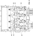
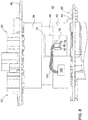
- an electronic inverter assembly 32 comprises an inverter power module 34.
- the inverter power module may comprise one or more switch modules 68.
- Each switch module 68 comprises one or more pairs of semiconductor switches mounted on a substrate.
- Each pair of semiconductors comprises a low-side semiconductor switch 36 and a high-side semiconductor switch 38.
- the semiconductor switches could be made of silicon carbide (SiC), gallium nitride (GaN), or any wide-bandgap semiconductor material.
- the semiconductor switches could be any of the following types of power transistors: metal oxide semiconductor field effect transistor (MOSFET), insulated gate bipolar junction transistor (IGBT), bipolar junction transistors (BJT), and the like.
- MOSFET metal oxide semiconductor field effect transistor
- IGBT insulated gate bipolar junction transistor
- BJT bipolar junction transistors
- Each of the semiconductor switches comprises a control terminal 40 and switched terminals 42.
- a first circuit board 44 has an outer side 151 adjacent to or that faces the inverter power module 34 and a first inner side 152 opposite the outer side 151.
- a first driver portion 48 comprises a set of first components 60 mounted on or associated with the first circuit board 44.
- a second circuit board 46 is spaced apart from the first circuit board 44.
- the second circuit board 46 has a second inner side 153 facing the first inner side 152.
- a second outer side 154 of the second circuit board 46 is opposite the second inner side 153.
- a second driver portion 50 comprises a set of second components 62 mounted on or associated with the second circuit board 46, where the first driver portion 48 and the second driver portion 50 collectively are adapted to provide input signals to the control terminal 40 of each semiconductor switch.
- a first edge connector 52 is mounted on the first inner side 152 of the first circuit board 44.
- a second edge connector 54 is mounted on the second inner side 153 of the second circuit board 46.
- An interface board 56 with mating edges 58 that mate with corresponding receptacles or slots in the first edge connector 52 and the second edge connector 54.
- the first components 60 comprises driver circuit components with higher temperature operating ranges than the second components 62.
- the first components 60 have a first temperature operating range of greater than or approximately equal to 150 degrees Celsius.
- the second components 62 comprise driver circuit components with a second temperature operating range of between approximately 125 degrees Celsius and approximately 150 degrees Celsius.
- the first circuit board 44 may be reserved for population by first components 60 with a higher temperature operating range than the second components 62 of the second circuit board 46.
- the driver comprises the first driver portion 48 and the second driver portion 50.
- the first driver portion 48 comprises the first circuit board 44 and the first components 60
- the second driver portion 50 comprises the second circuit board 46 and the second components 62.
- the first driver portion 48 and the second driver portion 50 form a driver circuit (e.g., low inductance driver circuit) via one or more interface boards 56 for providing control signals to the inverter or control terminals 40 (e.g., gates or bases) of the semiconductor switches of the switch modules 68.
- a driver circuit e.g., low inductance driver circuit
- a set of first edge connectors 52 are mounted on the first inner side 152 of the first circuit board 44.
- a set of second edge connectors 54 are mounted on the second inner side 153 of the second circuit board 46.
- each first edge connector 52 and each second edge connector 54 may comprise a surface mount card edge connector, such as those that are available through Sullins Connector Solutions of San Marcos, California.
- Each interface board 56 has mating edges 58 that mate with a corresponding one of the first edge connector 52 and a corresponding one of the second edge connector 54. For example, the mating edges 58 mate with corresponding slots or receptacles in the connectors (52, 54).
- Each interface board 56 and its corresponding edge connectors supports a suitable or low inductance signal path for electrical signals of the driver circuit (58, 50) that are communicated between the first board 44 and the second board 46, or between the first board 44 and the control terminal 40 of the respective semiconductor switch (36, 38) of the switching module 68 of the inverter, or between the second board 46 and the control terminal 40 of the respective semiconductor switch (36, 38) of the switching module 68 of the inverter.
- the first circuit board 44 has a first zone 64 (e.g., low inductance zone) near or within a maximum conductive trace length on the first circuit board 44 from the first edge connector 52 to minimize inductance provided to the control terminals 40 of the semiconductor switches (36, 38).
- the conductive traces are composed of metal, alloy or metallic material.
- the first zone 64 may contain circuits that would otherwise be susceptible to time delay from signal communication outside of the first zone 64.
- the first zone 64 can include first components 60 mounted on one or both sides of the first circuit board 44.
- the second circuit board 46 has a second zone 66 (e.g., low inductance zone) near or within a maximum conductive trace length on the circuit board from the second edge connector 54 to minimize inductance provided to the control terminals 40 of the semiconductor switches.
- the second zone 66 may contain circuits that would otherwise be susceptible to time delay from signal communication outside of the second zone 66.
- the second zone 66 can include second components 62 mounted on one or both sides of the second circuit board 46.
- conductive traces on the first circuit board 44 and the second circuit board 46 can be surrounded by one or more ground traces or ground planes to avoid loop current.
- conductive trace geometry can be arranged to group and separate conductive traces into three voltage classes: (1) high-voltage power traces/circuit referenced to high-side semiconductor switch 38 (e.g., metal oxide semiconductor field effect transistor (MOSFET)), (2) high-voltage power traces/circuit referenced to low-side semiconductor switch 36 (e.g., MOSFET), and (3) low-voltage power traces/circuit referenced to low-voltage electronics.
- high-voltage power traces/circuit referenced to high-side semiconductor switch 38 e.g., metal oxide semiconductor field effect transistor (MOSFET)
- MOSFET metal oxide semiconductor field effect transistor
- circuit board conductive traces are physically separated for necessary creepage (e.g., from thermal expansion and contraction) and clearance to meet high-voltage safety requirements and to eliminate cross-talk between time critical and performance critical circuits that serve different phases (e.g., three phases plus an optional brake chopper for single inverter) of the electronic inverter assembly 32 or inverter.
- the inverter assembly 32 may provide one or more phase output signals, such as alternating current output signals for a first phase, a second phase and a third phase. Further, the inverter assembly 32 may provide an optional fourth phase output as a brake chopper. If the inverter assembly is dual inverter configuration, the inverter assembly 32 further comprises a third circuit board 144 that is similar to the first circuit board 44.
- the third circuit board 144 can contain a driver circuit to drive one or more switch modules 68 or semiconductor switches (36, 38). The output of the switch modules can be at phase terminals or bus bar terminals.
- the direct current terminals 71 of the first circuit board 44 and the third circuit board 144 can be interconnected by a coaxial bus connector 145.
- a primary inverter may be used in a motoring mode to control the motor 88, whereas a secondary inverter may be used in a power generation mode to convert alternating current energy into direct current energy., or in a motoring mode to control another motor or auxiliary electric machine.
- the first circuit board 44 is reserved for components (e.g., first components 60), circuits or both that have a first temperature operating range of greater than or approximately equal to 150 degrees Celsius.
- the second circuit board 46 is reserved for components (e.g., second components 62), circuits, or both have a second temperature operating range of between approximately 125 degrees Celsius and approximately 150 degrees Celsius.
- the driver circuit 49 for the switching semiconductors of the inverter or dual inverter is split or divided into two circuit boards: the first driver portion 48 on the first circuit board 44 and the second driver portion 50 on the second circuit board 46, where the electrical connection and electrical signals communicated between the two circuit boards are subject to sufficiently low inductance. As used herein, approximately shall mean a tolerance of about plus or minus ten percent.
- the electronic inverter assembly 32 may be enclosed in a housing 155 with one or more coolant passages.
- engine coolant e.g., water and ethylene glycol
- the use of engine coolant for cooling the electronic inverter assembly 32 allows simplification of the vehicle because a separate dedicated cooling system for inverter can be eliminated.
- the electronic inverter assembly 32 can share or leverage the coolant pump and radiator of the vehicle for cooling of the electronic circuitry of the inverter assembly 32, for example. Elimination of a dedicated cooling system for inverter can result in a more compact design with a given power density required to support an electric drive system.
- the first circuit board 44 (e.g., lower circuit board) uses higher temperature components and is placed over switch modules 68 or inverter power module 34.
- the first circuit board 44 may be positioned above, facing, or adjacent to the ribs or protrusions of the switch modules 68 of the inverter, where the ribs or protrusions are configured to dissipate heat or thermal energy to the ambient air.
- one or more switch modules 68 may be mounted on or in contact with the first circuit board 44.
- the second circuit board 46 (e.g., upper circuit board) can be designed with the relatively low temperature parts. Interconnections used for electrical connections between first circuit board 44 and the second circuit board 46 must have lowest possible inductance, and different high voltage circuits should not electrically and magnetically interact with each-other to avoid cross-talk and malfunction of gate drive.
- the built-in current sensor 76 of the interface board 56 can potentially reduce inverter cost, eliminate a separate connector used for current-sensing circuit, and minimize the size of electronic inverter assembly 32 (e.g., inverter).
- the interface boards 56 alone or coupled with the first zone 64 and the second zone 66, are well suited for forming low inductance connections for the circuitry of the inverter 32 and miniaturization of the current sensor 76 integrated with the connector assembly.
- the driver circuit 49 or driver comprises a high-side driver circuit referenced to a high-side semiconductor switch 38 (e.g., SiC metal oxide semiconductor field effect transistor (MOSFET)), a low-side driver circuit referenced to a low-side semiconductor switch 36 (e.g., SiC metal oxide semiconductor field effect transistor (MOSFET)).
- a high-side driver circuit referenced to a high-side semiconductor switch 38 (e.g., SiC metal oxide semiconductor field effect transistor (MOSFET)
- MOSFET SiC metal oxide semiconductor field effect transistor
- the interface board 56, the first circuit board 44, and the second circuit board 46 comprises a dielectric layer of a polymer, a plastic, a polymer composite, a plastic composite, a fiber reinforced polymer, a fiber reinforced plastic, or a ceramic material.
- Conductive traces may overlie the dielectric layer on one or both sides of the interface board 56, the first circuit board 44, and the second circuit board 46.
- the conductive traces are composed of a metal, an alloy or metallic material.
- the conductive traces on opposite sides of any circuit board may be interconnected by conductive vias or conductive through-holes.
- the interface board 56 comprises a current sensor board with an opening 70 for receiving an output phase terminal 72, such as a bus bar or conductor with a rectangular, polygonal or elliptical cross section.
- the output phase terminal 72 has a cross section (e.g., rectangular cross section) that can pass through the opening 70 or a corresponding slit in the inductor or current-sensing coil 74.
- Each output phase terminal 72 is configured to output a signal produced by a pair of semiconductor switches or switch module 68.
- the interface board 56 (e.g., or board that also comprises current-sensing coil) comprises a plurality of conductive traces routed through conductive vias (e.g., metallic plated vias) between two adjacent internal conductive layers of the interface board 56.
- the above conductive traces form an inductor or a current-sensing coil 74 for inductively coupling the electromagnetic field in the output phase terminal 72 to a corresponding current sensor 76 circuit, such as the circuit of FIG. 10 .
- the coil 74 may comprise a time-varying flux sensing (e.g., TVFS) coil 74 that is electromagnetically coupled to the output phase terminal 72 and this electrically coupled to a current sensor 76 circuit.
- the coil 74 comprises a series of conductive traces (e.g., metallic traces) that are interconnected with conductive vias (e.g., metal-plated vias or through-holes) between two adjacent layers of interface board 56.
- the current sensor 76 can operate at the first temperature range, the second temperature range, or intermediate temperature ranges between the first temperature range and the second temperature range.
- the current sensor 76 has a bandwidth of sufficient frequency range to support a target sampling rate for accurate and timely current measurements in real time as the electronic inverter assembly 32 operates to control one or more motors 88, or to convert alternating current into direct current.
- the current sensor 76 comprises one or more of the following: (1) primary current sensor of conductive traces of the coil 74, (2) secondary current sensor of a magnetic field sensor 80 (e.g., Hall effect sensor) overlying at least a portion of the output phase terminal 72, and (3) secondary current sensor of a magnetic field sensor 80 and one or more flux concentrators 78 on opposite sides of the magnetic field sensor 80.
- a magnetic field sensor 80 e.g., Hall effect sensor
- the primary current sensor can have a plurality of conductive traces, on the interface board 56, that form an inductor or a current-sensing coil 74 for inductively coupling the current in the output phase terminal 72 to a current sensor 76.
- a secondary current sensor is associated with the output phase terminal 72.
- the secondary current sensor 76 comprises a magnetic field sensor 80 mounted on or near the output phase terminal 72.
- One or more flux concentrators 78 are disposed laterally with respect to the magnetic field sensor 80.
- a sensor processing circuit 22 can convert the sensed magnetic field into a respective current signal or digital representation of the current signal.
- the current sensor 76 can use ferrous metal shielding or filtering (e.g., ferrite core coils or ferrite beads) to eliminate electromagnetic cross-talk and interaction among inverter phases including the optional brake chopper unit.
- ferrous metal shielding or filtering e.g., ferrite core coils or ferrite beads
- the first sensed current from the coil 74 is fused or combined with a second sensed current from the magnetic field sensor 80, wherein the coil 74 comprises a time-varying flux sensing coil 74.
- the magnetic field sensor 80 is mounted on a respective interface board 56. Further, the magnetic field sensor 80 (e.g., Hall effect sensor) is surrounded by flux concentrators, or electromagnetic field concentrators to direct or focus the electromagnetic field produced by the electrical current in the output phase terminal 72 toward the magnetic field sensor 80 for detection thereby.
- the magnetic field sensor 80 e.g., Hall effect sensor
- the magnetic field sensor 80 is surrounded by flux concentrators, or electromagnetic field concentrators to direct or focus the electromagnetic field produced by the electrical current in the output phase terminal 72 toward the magnetic field sensor 80 for detection thereby.
- a multi-conductor cable (e.g., ribbon cable) 161 or transmission line terminates in a multi-conductor connector 163 at a first end and is electrically connected to the secondary current sensor 76 or magnetic field sensor 80 at the second end.
- the multi-conductor connector 163 may be mounted on the first circuit board 44 or otherwise electrically connected to the current sensor 76,
- the multi-conductor cable 161 is arranged for connecting to secondary current sensor 76 (e.g., the magnetic field sensor 80) to provide the signals to signal processing circuit, such as that illustrated in the block diagram of FIG. 10 .
- the magnetic field sensor 80 is mounted on or overlies the output phase terminal 72.
- the first circuit board 44 has first set of first edge connectors 52 on the first inner side 152; the second circuit board 46 has a second set of second edge connectors 54 on the second inner side 153.
- a set of interface boards 56 is arranged or adapted for interconnecting the first driver portion 48 and the second driver portion 50. As illustrated in the drawings, each interface board 56 handles or services one phase of the inverter, although in alternate embodiments an interface board may service multiple phases of the inverter.
- the interface board 56 supports low inductance connections for the input signals (e.g., driver control signals) to the control terminals 40 of the semiconductor switches of one or more switch modules 68, where the input signals are generated by the first components 60 and the second components 62, collectively.
- the first edge connectors 52 comprise three sets of traces.
- the first set of traces 82 e.g., left-most traces
- the second set of traces 84 e.g., center traces
- the third set of traces 86 (right-most traces) are for signaling the low-side semiconductor switch 36 in a respective switch modules 68.
- the third set of traces 86 can include ancillary or supplemental traces for carrying additional signals, such as, temperature of power semiconductor module 68.
- the coil 74 is located radially outward from the output phase terminal 72 and may be formed of wire windings, insulated conductors, or circuit traces on one or more sides of the dielectric substrate of the interface board 56.
- the semiconductor switches (36, 38) comprise silicon carbide (SiC) or gallium (GaN) nitride switches or transistors.
- SiC silicon carbide
- GaN gallium
- each phase may be packaged as a separate switch module 68 comprising a low-side switch 36 and high-side switch 38 with ones of the switched terminals 42 coupled together at a phase output node 69 and others of the switched terminals 42 coupled between the terminals of the direct current bus 71.
- three switch modules 68 may be used for a three phase inverter, or four switch modules 68 may be used for a three phase inverter with the fourth switch module 68 is used for a brake chopper to provide regenerative energy to charge an energy storage device, such as a battery.
- the switch module 68 has control terminals 40 of the high-side switch 38 and the low side switch 36 for receiving input signals or control signals from the driver 49, which resides on the first circuit board 44 and the second circuit board 46.
- Each phase has an output node 69 that is coupled to an electric motor 88.
- the switched terminals 42 comprise an emitter and a collector and the control terminal 40 comprises a base or gate.
- the semiconductor switches (36, 38) comprise field effect transistors, the switched terminals 42 comprise a source and drain and the control terminal 40 comprises a gate.
- the inverter power module 34 comprises a dual inverter having a primary inverter (e.g., of three phases plus a brake chopper phase) and a secondary inverter (e.g., of three phases only), where the primary inverter is mounted on a primary substrate that faces a secondary inverter mounted on a secondary substrate.
- a primary inverter e.g., of three phases plus a brake chopper phase
- a secondary inverter e.g., of three phases only
- FIG. 10 is a block diagram of a current-sensing circuit.
- magnetic field sensor 80 senses at least a direct current signal component of the observed signal in the conductor or output phase terminal 72.
- the magnetic field sensor 80 senses a direct current signal component and a lower frequency signal component (or second alternating signal component) of the alternating current signal in the conductor or output phase terminal 72.
- the second alternating signal component is lower in frequency than the first alternating signal component.
- the current sensor 76 comprises circuitry 22 or low voltage electronics.
- the circuitry 22 has a first filtering circuit 26 and a second filtering circuit 28 that are coupled to a sensor fusion circuit 30.
- the circuitry 22 further comprises a current change detector 24 that is capable of receiving an alternating current signal from the inductor or current-sensing coil 74.
- a first filtering circuit 26 has a high-pass filter response.
- the first filtering circuit 26 is coupled to the inductor 74 to provide a filtered alternating current signal component (e.g., first alternating signal component).
- a second filtering circuit 28 has a low-pass filter response.
- the second filtering circuit 28 coupled to the magnetic field sensor 80 to provide: (1) a filtered direct current signal component, (2) a lower frequency alternating signal component (e.g., second alternating signal component), or both.
- a sensor fusion circuit 30 determines an aggregate sensed current (e.g., in the output phase terminal 72) based on the filtered alternating current signal component and the filtered direct current signal component.
- the aggregate sensed current (e.g., in each output phase terminal 72) refers to the combined current that includes contributions of the direct current signal components and alternating signal components.
- the electronic inverter assembly 32 is well suited for reducing cost by limiting or minimizing the components that need to operate at the first temperature range.
- the electronic inverter assembly 32 can facilitate or leverage the use of engine coolant for cooling the electronic inverter at target power densities, such power densities per volume as greater than approximately 25 kW/L (kilowatt per liter).
- target power densities such power densities per volume as greater than approximately 25 kW/L (kilowatt per liter).
- nH nano-Henries
- the electronic inverter assembly 32 can be configured as a higher-power density Silicon Carbide (SiC) inverter that are cooled by engine coolant.
- SiC Silicon Carbide
- the inverter assembly comprises a first interface board 56 for a first phase, a second interface board 56 for a second phase and a third interface board 56 for a third phase that provide electrical and mechanical connections between the first driver portion 48 of the first circuit board 44 and the second driver portion 50 of the second circuit board 46.
- Each interface board 56 is associated with a current sensor 76 or current-sensing module.
- the first interface board 56 is associated with a first current sensor 76 for sensing electrical current in the first output phase terminal 72 of the first phase; the second interface board 56 is associated with a second current sensor 76 for sensing electrical current in the second output phase terminal 72 of the second phase; the third interface board 56 is associated with a third current sensor 76 for sensing electrical current in the third output phase terminal 72 of the third phase.
- the driver 49 comprises the first driver portion 48 and the second driver portion 50 collectively that provide control signals to the control inputs 40 of the semiconductor switches (36, 38) for each phase.
- the dashed lines between each interface board 56 or the current sensor 76 represent inductive coupling between the output phase terminals (72) that are coupled to the motor 88 or electric machine.
Landscapes
- Engineering & Computer Science (AREA)
- Microelectronics & Electronic Packaging (AREA)
- Power Engineering (AREA)
- Physics & Mathematics (AREA)
- Thermal Sciences (AREA)
- General Physics & Mathematics (AREA)
- Inverter Devices (AREA)
Claims (14)
- Elektronische Stromrichteranordnung (32), wobei die Anordnung Folgendes aufweist:ein Stromrichterleistungsmodul (34), das ein oder mehr Halbleiterschalterpaare, die auf einem Träger montiert sind, aufweist, wobei jedes Halbleiterpaar einen Low-Side-Halbleiterschalter (36) und einen High-Side-Halbleiterschalter (38) aufweist, wobei jeder der Halbleiterschalter einen Steueranschluss und geschaltete Anschlüsse aufweist;eine erste Leiterplatte (44) mit einer Außenseite (151), die an das bzw. dem Stromrichterleistungsmodul angrenzt oder gegenüberliegt, und einer der Außenseite entgegengesetzten ersten Innenseite (152);einen ersten Treiberteil (48), der einen Satz erster Komponenten (60) aufweist, die an oder mit der ersten Leiterplatte montiert oder zugeordnet sind;eine zweite Leiterplatte (46), die von der ersten Leiterplatte beabstandet ist, wobei die zweite Leiterplatte eine zweite Innenseite (153) hat, die der ersten Innenseite (152) gegenüberliegt;einen zweiten Treiberteil (50), der einen Satz zweiter Komponenten (62) aufweist, die an oder mit der zweiten Leiterplatte montiert oder zugeordnet sind, wobei der erste Treiberteil (48) und der zweite Treiberteil (46) gemeinsam zum Anlegen von Eingangssignalen an den Steueranschluss jedes Halbleiterschalters (36, 38) ausgeführt sind;einen ersten Platinenstecker (52), der an der ersten Innenseite (152) der ersten Leiterplatte (44) montiert ist;einen zweiten Platinenstecker (54), der an der zweiten Innenseite (153) der zweiten Leiterplatte (46) montiert ist;eine Schnittstellenkarte (56) mit Gegenrändern (58), die mit dem ersten Platinenstecker (52) und dem zweiten Platinenstecker (54) zusammenpassen; undwobei die ersten Komponenten (60) Komponenten mit Betriebsbereichen mit höherer Temperatur als die zweiten Komponenten aufweisen.
- Anordnung nach Anspruch 1, wobei die ersten Komponenten (60) einen Betriebsbereich mit einer ersten Temperatur haben, die größer oder etwa gleich 150 Grad Celsius ist.
- Anordnung nach Anspruch 1 oder 2, wobei die zweiten Komponenten (62) einen Betriebsbereich mit einer zweiten Temperatur zwischen etwa 125 Grad Celsius und etwa 150 Grad Celsius haben.
- Anordnung nach einem der vorhergehenden Ansprüche, wobei die Schnittstellenkarte (56) eine Stromsensorkarte mit einer Öffnung (70) für einen Ausgangsphasenanschluss (72) einer Ausgangsphase eines Halbleiterschalterpaares aufweist.
- Anordnung nach einem der vorhergehenden Ansprüche, wobei die Stromsensorkarte mehrere Leiterbahnen aufweist, die eine Induktionsspule oder eine Stromerfassungsspule (74) zum induktiven Koppeln eines Stromsensors auf der Stromsensorkarte mit dem Ausgangsphasenanschluss (72) bilden.
- Anordnung nach Anspruch 5, wobei der Ausgangsphasenanschluss (72) einen Querschnitt hat, der durch die Öffnung oder einen entsprechenden Schlitz in der Induktionsspule oder Stromerfassungsspule hindurchgeführt werden kann.
- Anordnung nach einem der vorhergehenden Ansprüche, wobei der Stromsensor Folgendes aufweist:einen Magnetfeldsensor (80), der wenigstens einen Teil der Leiterbahnen der Spule überlagern kann;ein oder mehr Flussleitstücke an einander entgegengesetzten Seiten des Magnetfeldsensors.
- Anordnung nach Anspruch 7, wobei der Stromsensor ferner mehrere Leiterbahnen aufweist, die eine Induktionsspule oder eine Stromerfassungsspule (74) zum induktiven Koppeln eines Stromsensors auf der Stromsensorkarte mit dem Ausgangsphasenanschluss (72) bilden.
- Anordnung nach Anspruch 8, wobei ein erster erfasster Strom vom Magnetfeldsensor mit einem zweiten erfassten Strom von der Spule verschmolzen oder kombiniert wird, wobei die Spule eine zeitvarianten Fluss erfassende Spule umfasst.
- Anordnung nach einem der vorhergehenden Ansprüche, wobei ein sekundärer Stromsensor (76) dem Ausgangsphasenanschluss zugeordnet ist, wobei der sekundäre Stromsensor Folgendes aufweist:einen Magnetfeldsensor, der an dem oder nahe an dem Ausgangsphasenanschluss montiert ist;ein oder mehr Flussleitstücke, die in Bezug auf den Magnetfeldsensor seitlich angeordnet sind; undeinen Mehrleiterstecker zum Verbinden mit dem Magnetfeldsensor.
- Anordnung nach einem der vorhergehenden Ansprüche, wobei die erste Leiterplatte eine erste Vielzahl von ersten Platinensteckern (52) auf der ersten Innenseite hat, die zweite Leiterplatte eine zweite Vielzahl von zweiten Platinensteckern (54) auf der zweiten Innenseite hat und ferner mehrere Schnittstellenkarten zum Zusammenschalten des ersten Treiberteils und des zweiten Treiberteils aufweist.
- Anordnung nach Anspruch 11, wobei die Schnittstellenkarte Verbindungen niedriger Induktivität für die Eingangssignale der Steueranschlüsse der Halbleiterschalter (36, 38) unterstützt, wobei die Eingangssignale durch die ersten Komponenten (60) und die zweiten Komponenten (62) gemeinsam erzeugt werden.
- Anordnung nach Anspruch 1, wobei die Halbleiterschalter Siliziumkarbid oder Galliumnitrid aufweisen.
- Anordnung nach einem der vorhergehenden Ansprüche, wobei das Stromrichterleistungsmodul einen Doppelstromrichter mit einem primären Stromrichter und einem sekundären Stromrichter umfasst, wobei der primäre Stromrichter auf einem primären Träger montiert ist, der einem sekundären Stromrichter gegenüberliegt, der auf einem sekundären Träger montiert ist.
Applications Claiming Priority (1)
| Application Number | Priority Date | Filing Date | Title |
|---|---|---|---|
| US15/248,241 US9979320B2 (en) | 2016-08-26 | 2016-08-26 | Electronic inverter assembly |
Publications (2)
| Publication Number | Publication Date |
|---|---|
| EP3288358A1 EP3288358A1 (de) | 2018-02-28 |
| EP3288358B1 true EP3288358B1 (de) | 2020-03-25 |
Family
ID=59649449
Family Applications (1)
| Application Number | Title | Priority Date | Filing Date |
|---|---|---|---|
| EP17183402.1A Active EP3288358B1 (de) | 2016-08-26 | 2017-07-26 | Elektronische wechselrichterbaugruppe |
Country Status (2)
| Country | Link |
|---|---|
| US (1) | US9979320B2 (de) |
| EP (1) | EP3288358B1 (de) |
Families Citing this family (4)
| Publication number | Priority date | Publication date | Assignee | Title |
|---|---|---|---|---|
| US12225657B2 (en) * | 2017-01-03 | 2025-02-11 | Transportation Ip Holdings, Llc | Power system and method for controlling power modules |
| EP3462822A1 (de) * | 2017-09-29 | 2019-04-03 | Siemens Aktiengesellschaft | Elektrischer umrichter |
| US10720852B1 (en) * | 2019-01-30 | 2020-07-21 | The United States Of America As Represented By The Secretary Of The Army | High power direct current/alternating current inverter |
| KR102334500B1 (ko) * | 2019-02-18 | 2021-12-02 | 엘에스일렉트릭(주) | 모듈형 인버터 시스템 |
Family Cites Families (28)
| Publication number | Priority date | Publication date | Assignee | Title |
|---|---|---|---|---|
| US5699609A (en) | 1995-04-12 | 1997-12-23 | Allen-Bradley Company, Inc. | Method of making power substrate assembly |
| DE19847028A1 (de) | 1998-10-13 | 2000-04-27 | Semikron Elektronik Gmbh | Kondensator für niederinduktive Zwischenkreisaufbauten |
| US6278603B1 (en) | 1999-03-08 | 2001-08-21 | Acumentrics Corporation | Low inductance capacitor |
| GB2356752B (en) | 1999-11-29 | 2004-08-11 | Eev Ltd | Switching arrangements |
| JP3774624B2 (ja) * | 2000-10-18 | 2006-05-17 | 三菱電機株式会社 | 電動パワーステアリング装置 |
| FR2871022B1 (fr) | 2004-05-25 | 2006-11-03 | Valeo Electronique Sys Liaison | Boitier pour circuits electriques ou electroniques |
| US7289311B2 (en) | 2004-06-09 | 2007-10-30 | Sbe Inc. | Power ring pulse capacitor |
| JP4284531B2 (ja) | 2004-07-06 | 2009-06-24 | オムロン株式会社 | 実装用基板及びそれを使用した駆動装置 |
| US7453114B2 (en) | 2005-08-05 | 2008-11-18 | Sbe, Inc. | Segmented end electrode capacitor and method of segmenting an end electrode of a capacitor |
| JP4931458B2 (ja) * | 2006-04-06 | 2012-05-16 | 日立オートモティブシステムズ株式会社 | 電力変換装置 |
| JP4850564B2 (ja) * | 2006-04-06 | 2012-01-11 | 日立オートモティブシステムズ株式会社 | 電力変換装置 |
| EP2171836A4 (de) | 2007-07-09 | 2015-06-10 | Power Concepts Nz Ltd | Schichtstrukturverbindung und baugruppe |
| US7800331B2 (en) * | 2007-11-27 | 2010-09-21 | Gm Global Technology Operations, Inc. | Method and system for operating an electric motor coupled to multiple power supplies |
| JP5171520B2 (ja) | 2008-09-30 | 2013-03-27 | 日立オートモティブシステムズ株式会社 | 電力変換装置 |
| JP5422466B2 (ja) * | 2010-04-01 | 2014-02-19 | 日立オートモティブシステムズ株式会社 | 電力変換装置 |
| JP5201171B2 (ja) * | 2010-05-21 | 2013-06-05 | 株式会社デンソー | 半導体モジュール、および、それを用いた駆動装置 |
| US20120229977A1 (en) | 2011-03-11 | 2012-09-13 | S B E, Inc. | Coaxial Capacitor Bus Termination |
| JP5651552B2 (ja) * | 2011-07-22 | 2015-01-14 | 日立オートモティブシステムズ株式会社 | 電力変換装置 |
| US9030822B2 (en) * | 2011-08-15 | 2015-05-12 | Lear Corporation | Power module cooling system |
| US9295184B2 (en) * | 2012-12-14 | 2016-03-22 | GM Global Technology Operations LLC | Scalable and modular approach for power electronic building block design in automotive applications |
| US9297836B2 (en) * | 2013-03-08 | 2016-03-29 | Deere & Company | Method and sensor for sensing current in a conductor |
| US9410990B2 (en) * | 2013-03-08 | 2016-08-09 | Deere & Company | Method and sensor for sensing current in a conductor |
| US9935558B2 (en) | 2013-10-07 | 2018-04-03 | Hitachi Automotive Systems, Ltd. | DC-DC converter apparatus including single drive circuit board arranged at predetermined interval from metal base |
| JP2015089245A (ja) | 2013-10-31 | 2015-05-07 | Ntn株式会社 | 車両駆動モータ用インバータ装置 |
| WO2015112717A1 (en) * | 2014-01-22 | 2015-07-30 | Amphenol Corporation | High speed, high density electrical connector with shielded signal paths |
| EP2953434A1 (de) | 2014-06-05 | 2015-12-09 | Home Control Singapore Pte. Ltd. | Anordnung elektronischer Leiterplatten |
| US10193417B2 (en) * | 2014-12-18 | 2019-01-29 | Black & Decker Inc. | Brushless motor assembly for a fastening tool |
| US9722531B2 (en) * | 2015-05-22 | 2017-08-01 | Deere & Company | Electronic inverter assembly with an integral snubber capacitor |
-
2016
- 2016-08-26 US US15/248,241 patent/US9979320B2/en active Active
-
2017
- 2017-07-26 EP EP17183402.1A patent/EP3288358B1/de active Active
Non-Patent Citations (1)
| Title |
|---|
| None * |
Also Published As
| Publication number | Publication date |
|---|---|
| US9979320B2 (en) | 2018-05-22 |
| EP3288358A1 (de) | 2018-02-28 |
| US20180062539A1 (en) | 2018-03-01 |
Similar Documents
| Publication | Publication Date | Title |
|---|---|---|
| US9722531B2 (en) | Electronic inverter assembly with an integral snubber capacitor | |
| JP7297815B2 (ja) | パワーデバイスを並列接続するための低インダクタンスおよび高速スイッチングを有するハイパワー多層モジュール | |
| US11678468B2 (en) | High density power module | |
| US11018109B2 (en) | Power semiconductor module with low gate path inductance | |
| US10811958B2 (en) | Water-cooling power supply module | |
| US11527456B2 (en) | Power module with organic layers | |
| CN107393715B (zh) | 电容器、尤其用于多相系统的中间电路电容器 | |
| US9979320B2 (en) | Electronic inverter assembly | |
| US20230307376A1 (en) | Power Semiconductor Module with Two Opposite Half-Bridges | |
| EP3506725B1 (de) | Elektronische anordnung mit verbesserter hoher leistungsdichte | |
| EP3288357B1 (de) | Elektronische wechselrichteranordnung mit einem integrierten dämpferkondensator | |
| JP2001274322A (ja) | パワー半導体モジュール | |
| US8487416B2 (en) | Coaxial power module | |
| US11476737B2 (en) | Integrated power control assemblies with built-in cooling systems | |
| CN118137782A (zh) | 具有改进的信号引脚场屏蔽的用于转换器的功率模块 | |
| US12394766B2 (en) | Assembly of semiconductor power modules | |
| CN118589805A (zh) | 功率模块、电机控制器及用电设备 | |
| EP4432317A1 (de) | Transformatoranordnung | |
| KR20250075237A (ko) | 파워 모듈 | |
| KR20160092945A (ko) | 회전 자계 기기용 출력 제어 장치 | |
| CN223957441U (zh) | 一种功率砖和电子设备 | |
| CN118588696B (zh) | 一种功率模块 | |
| CN118588633B (zh) | 功率模块组件的制造方法及功率模块组件 | |
| EP4636792A1 (de) | Sammelschienenfilter | |
| WO2022229034A1 (en) | Power module with parallel-switched semiconductor components |
Legal Events
| Date | Code | Title | Description |
|---|---|---|---|
| PUAI | Public reference made under article 153(3) epc to a published international application that has entered the european phase |
Free format text: ORIGINAL CODE: 0009012 |
|
| STAA | Information on the status of an ep patent application or granted ep patent |
Free format text: STATUS: THE APPLICATION HAS BEEN PUBLISHED |
|
| AK | Designated contracting states |
Kind code of ref document: A1 Designated state(s): AL AT BE BG CH CY CZ DE DK EE ES FI FR GB GR HR HU IE IS IT LI LT LU LV MC MK MT NL NO PL PT RO RS SE SI SK SM TR |
|
| AX | Request for extension of the european patent |
Extension state: BA ME |
|
| STAA | Information on the status of an ep patent application or granted ep patent |
Free format text: STATUS: REQUEST FOR EXAMINATION WAS MADE |
|
| 17P | Request for examination filed |
Effective date: 20180828 |
|
| RBV | Designated contracting states (corrected) |
Designated state(s): AL AT BE BG CH CY CZ DE DK EE ES FI FR GB GR HR HU IE IS IT LI LT LU LV MC MK MT NL NO PL PT RO RS SE SI SK SM TR |
|
| GRAP | Despatch of communication of intention to grant a patent |
Free format text: ORIGINAL CODE: EPIDOSNIGR1 |
|
| STAA | Information on the status of an ep patent application or granted ep patent |
Free format text: STATUS: GRANT OF PATENT IS INTENDED |
|
| INTG | Intention to grant announced |
Effective date: 20191213 |
|
| GRAS | Grant fee paid |
Free format text: ORIGINAL CODE: EPIDOSNIGR3 |
|
| GRAA | (expected) grant |
Free format text: ORIGINAL CODE: 0009210 |
|
| STAA | Information on the status of an ep patent application or granted ep patent |
Free format text: STATUS: THE PATENT HAS BEEN GRANTED |
|
| AK | Designated contracting states |
Kind code of ref document: B1 Designated state(s): AL AT BE BG CH CY CZ DE DK EE ES FI FR GB GR HR HU IE IS IT LI LT LU LV MC MK MT NL NO PL PT RO RS SE SI SK SM TR |
|
| REG | Reference to a national code |
Ref country code: GB Ref legal event code: FG4D |
|
| REG | Reference to a national code |
Ref country code: DE Ref legal event code: R096 Ref document number: 602017013495 Country of ref document: DE |
|
| REG | Reference to a national code |
Ref country code: AT Ref legal event code: REF Ref document number: 1250131 Country of ref document: AT Kind code of ref document: T Effective date: 20200415 Ref country code: IE Ref legal event code: FG4D |
|
| PG25 | Lapsed in a contracting state [announced via postgrant information from national office to epo] |
Ref country code: NO Free format text: LAPSE BECAUSE OF FAILURE TO SUBMIT A TRANSLATION OF THE DESCRIPTION OR TO PAY THE FEE WITHIN THE PRESCRIBED TIME-LIMIT Effective date: 20200625 Ref country code: FI Free format text: LAPSE BECAUSE OF FAILURE TO SUBMIT A TRANSLATION OF THE DESCRIPTION OR TO PAY THE FEE WITHIN THE PRESCRIBED TIME-LIMIT Effective date: 20200325 Ref country code: RS Free format text: LAPSE BECAUSE OF FAILURE TO SUBMIT A TRANSLATION OF THE DESCRIPTION OR TO PAY THE FEE WITHIN THE PRESCRIBED TIME-LIMIT Effective date: 20200325 |
|
| PG25 | Lapsed in a contracting state [announced via postgrant information from national office to epo] |
Ref country code: LV Free format text: LAPSE BECAUSE OF FAILURE TO SUBMIT A TRANSLATION OF THE DESCRIPTION OR TO PAY THE FEE WITHIN THE PRESCRIBED TIME-LIMIT Effective date: 20200325 Ref country code: SE Free format text: LAPSE BECAUSE OF FAILURE TO SUBMIT A TRANSLATION OF THE DESCRIPTION OR TO PAY THE FEE WITHIN THE PRESCRIBED TIME-LIMIT Effective date: 20200325 Ref country code: HR Free format text: LAPSE BECAUSE OF FAILURE TO SUBMIT A TRANSLATION OF THE DESCRIPTION OR TO PAY THE FEE WITHIN THE PRESCRIBED TIME-LIMIT Effective date: 20200325 Ref country code: BG Free format text: LAPSE BECAUSE OF FAILURE TO SUBMIT A TRANSLATION OF THE DESCRIPTION OR TO PAY THE FEE WITHIN THE PRESCRIBED TIME-LIMIT Effective date: 20200625 Ref country code: GR Free format text: LAPSE BECAUSE OF FAILURE TO SUBMIT A TRANSLATION OF THE DESCRIPTION OR TO PAY THE FEE WITHIN THE PRESCRIBED TIME-LIMIT Effective date: 20200626 |
|
| REG | Reference to a national code |
Ref country code: NL Ref legal event code: MP Effective date: 20200325 |
|
| REG | Reference to a national code |
Ref country code: LT Ref legal event code: MG4D |
|
| PG25 | Lapsed in a contracting state [announced via postgrant information from national office to epo] |
Ref country code: NL Free format text: LAPSE BECAUSE OF FAILURE TO SUBMIT A TRANSLATION OF THE DESCRIPTION OR TO PAY THE FEE WITHIN THE PRESCRIBED TIME-LIMIT Effective date: 20200325 |
|
| PG25 | Lapsed in a contracting state [announced via postgrant information from national office to epo] |
Ref country code: SM Free format text: LAPSE BECAUSE OF FAILURE TO SUBMIT A TRANSLATION OF THE DESCRIPTION OR TO PAY THE FEE WITHIN THE PRESCRIBED TIME-LIMIT Effective date: 20200325 Ref country code: EE Free format text: LAPSE BECAUSE OF FAILURE TO SUBMIT A TRANSLATION OF THE DESCRIPTION OR TO PAY THE FEE WITHIN THE PRESCRIBED TIME-LIMIT Effective date: 20200325 Ref country code: CZ Free format text: LAPSE BECAUSE OF FAILURE TO SUBMIT A TRANSLATION OF THE DESCRIPTION OR TO PAY THE FEE WITHIN THE PRESCRIBED TIME-LIMIT Effective date: 20200325 Ref country code: LT Free format text: LAPSE BECAUSE OF FAILURE TO SUBMIT A TRANSLATION OF THE DESCRIPTION OR TO PAY THE FEE WITHIN THE PRESCRIBED TIME-LIMIT Effective date: 20200325 Ref country code: RO Free format text: LAPSE BECAUSE OF FAILURE TO SUBMIT A TRANSLATION OF THE DESCRIPTION OR TO PAY THE FEE WITHIN THE PRESCRIBED TIME-LIMIT Effective date: 20200325 Ref country code: PT Free format text: LAPSE BECAUSE OF FAILURE TO SUBMIT A TRANSLATION OF THE DESCRIPTION OR TO PAY THE FEE WITHIN THE PRESCRIBED TIME-LIMIT Effective date: 20200818 Ref country code: SK Free format text: LAPSE BECAUSE OF FAILURE TO SUBMIT A TRANSLATION OF THE DESCRIPTION OR TO PAY THE FEE WITHIN THE PRESCRIBED TIME-LIMIT Effective date: 20200325 Ref country code: IS Free format text: LAPSE BECAUSE OF FAILURE TO SUBMIT A TRANSLATION OF THE DESCRIPTION OR TO PAY THE FEE WITHIN THE PRESCRIBED TIME-LIMIT Effective date: 20200725 |
|
| REG | Reference to a national code |
Ref country code: AT Ref legal event code: MK05 Ref document number: 1250131 Country of ref document: AT Kind code of ref document: T Effective date: 20200325 |
|
| REG | Reference to a national code |
Ref country code: DE Ref legal event code: R097 Ref document number: 602017013495 Country of ref document: DE |
|
| PG25 | Lapsed in a contracting state [announced via postgrant information from national office to epo] |
Ref country code: ES Free format text: LAPSE BECAUSE OF FAILURE TO SUBMIT A TRANSLATION OF THE DESCRIPTION OR TO PAY THE FEE WITHIN THE PRESCRIBED TIME-LIMIT Effective date: 20200325 Ref country code: AT Free format text: LAPSE BECAUSE OF FAILURE TO SUBMIT A TRANSLATION OF THE DESCRIPTION OR TO PAY THE FEE WITHIN THE PRESCRIBED TIME-LIMIT Effective date: 20200325 Ref country code: IT Free format text: LAPSE BECAUSE OF FAILURE TO SUBMIT A TRANSLATION OF THE DESCRIPTION OR TO PAY THE FEE WITHIN THE PRESCRIBED TIME-LIMIT Effective date: 20200325 Ref country code: DK Free format text: LAPSE BECAUSE OF FAILURE TO SUBMIT A TRANSLATION OF THE DESCRIPTION OR TO PAY THE FEE WITHIN THE PRESCRIBED TIME-LIMIT Effective date: 20200325 |
|
| PLBE | No opposition filed within time limit |
Free format text: ORIGINAL CODE: 0009261 |
|
| STAA | Information on the status of an ep patent application or granted ep patent |
Free format text: STATUS: NO OPPOSITION FILED WITHIN TIME LIMIT |
|
| PG25 | Lapsed in a contracting state [announced via postgrant information from national office to epo] |
Ref country code: MC Free format text: LAPSE BECAUSE OF FAILURE TO SUBMIT A TRANSLATION OF THE DESCRIPTION OR TO PAY THE FEE WITHIN THE PRESCRIBED TIME-LIMIT Effective date: 20200325 Ref country code: PL Free format text: LAPSE BECAUSE OF FAILURE TO SUBMIT A TRANSLATION OF THE DESCRIPTION OR TO PAY THE FEE WITHIN THE PRESCRIBED TIME-LIMIT Effective date: 20200325 |
|
| REG | Reference to a national code |
Ref country code: CH Ref legal event code: PL |
|
| 26N | No opposition filed |
Effective date: 20210112 |
|
| REG | Reference to a national code |
Ref country code: BE Ref legal event code: MM Effective date: 20200731 |
|
| PG25 | Lapsed in a contracting state [announced via postgrant information from national office to epo] |
Ref country code: LI Free format text: LAPSE BECAUSE OF NON-PAYMENT OF DUE FEES Effective date: 20200731 Ref country code: LU Free format text: LAPSE BECAUSE OF NON-PAYMENT OF DUE FEES Effective date: 20200726 Ref country code: CH Free format text: LAPSE BECAUSE OF NON-PAYMENT OF DUE FEES Effective date: 20200731 |
|
| PG25 | Lapsed in a contracting state [announced via postgrant information from national office to epo] |
Ref country code: BE Free format text: LAPSE BECAUSE OF NON-PAYMENT OF DUE FEES Effective date: 20200731 Ref country code: SI Free format text: LAPSE BECAUSE OF FAILURE TO SUBMIT A TRANSLATION OF THE DESCRIPTION OR TO PAY THE FEE WITHIN THE PRESCRIBED TIME-LIMIT Effective date: 20200325 |
|
| PG25 | Lapsed in a contracting state [announced via postgrant information from national office to epo] |
Ref country code: IE Free format text: LAPSE BECAUSE OF NON-PAYMENT OF DUE FEES Effective date: 20200726 |
|
| PG25 | Lapsed in a contracting state [announced via postgrant information from national office to epo] |
Ref country code: TR Free format text: LAPSE BECAUSE OF FAILURE TO SUBMIT A TRANSLATION OF THE DESCRIPTION OR TO PAY THE FEE WITHIN THE PRESCRIBED TIME-LIMIT Effective date: 20200325 Ref country code: MT Free format text: LAPSE BECAUSE OF FAILURE TO SUBMIT A TRANSLATION OF THE DESCRIPTION OR TO PAY THE FEE WITHIN THE PRESCRIBED TIME-LIMIT Effective date: 20200325 Ref country code: CY Free format text: LAPSE BECAUSE OF FAILURE TO SUBMIT A TRANSLATION OF THE DESCRIPTION OR TO PAY THE FEE WITHIN THE PRESCRIBED TIME-LIMIT Effective date: 20200325 |
|
| PG25 | Lapsed in a contracting state [announced via postgrant information from national office to epo] |
Ref country code: MK Free format text: LAPSE BECAUSE OF FAILURE TO SUBMIT A TRANSLATION OF THE DESCRIPTION OR TO PAY THE FEE WITHIN THE PRESCRIBED TIME-LIMIT Effective date: 20200325 Ref country code: AL Free format text: LAPSE BECAUSE OF FAILURE TO SUBMIT A TRANSLATION OF THE DESCRIPTION OR TO PAY THE FEE WITHIN THE PRESCRIBED TIME-LIMIT Effective date: 20200325 |
|
| PGFP | Annual fee paid to national office [announced via postgrant information from national office to epo] |
Ref country code: DE Payment date: 20250620 Year of fee payment: 9 |
|
| PGFP | Annual fee paid to national office [announced via postgrant information from national office to epo] |
Ref country code: GB Payment date: 20250728 Year of fee payment: 9 |
|
| PGFP | Annual fee paid to national office [announced via postgrant information from national office to epo] |
Ref country code: FR Payment date: 20250725 Year of fee payment: 9 |