EP3288166A1 - Control device for power converter - Google Patents
Control device for power converter Download PDFInfo
- Publication number
- EP3288166A1 EP3288166A1 EP16782844.1A EP16782844A EP3288166A1 EP 3288166 A1 EP3288166 A1 EP 3288166A1 EP 16782844 A EP16782844 A EP 16782844A EP 3288166 A1 EP3288166 A1 EP 3288166A1
- Authority
- EP
- European Patent Office
- Prior art keywords
- circuit
- current
- output
- constant
- control circuit
- Prior art date
- Legal status (The legal status is an assumption and is not a legal conclusion. Google has not performed a legal analysis and makes no representation as to the accuracy of the status listed.)
- Withdrawn
Links
Images


Classifications
-
- H—ELECTRICITY
- H02—GENERATION; CONVERSION OR DISTRIBUTION OF ELECTRIC POWER
- H02J—ELECTRIC POWER NETWORKS; CIRCUIT ARRANGEMENTS OR SYSTEMS FOR SUPPLYING OR DISTRIBUTING ELECTRIC POWER; SYSTEMS FOR STORING ELECTRIC ENERGY
- H02J1/00—Circuit arrangements for DC mains or DC distribution networks
- H02J1/02—Arrangements for reducing harmonics or ripples
-
- H—ELECTRICITY
- H02—GENERATION; CONVERSION OR DISTRIBUTION OF ELECTRIC POWER
- H02J—ELECTRIC POWER NETWORKS; CIRCUIT ARRANGEMENTS OR SYSTEMS FOR SUPPLYING OR DISTRIBUTING ELECTRIC POWER; SYSTEMS FOR STORING ELECTRIC ENERGY
- H02J3/00—Circuit arrangements for AC mains or AC distribution networks
- H02J3/36—Arrangements for transfer of electric power between AC networks via high-voltage DC [HVDC] links; Arrangements for transfer of electric power between generators and networks via HVDC links
-
- H—ELECTRICITY
- H02—GENERATION; CONVERSION OR DISTRIBUTION OF ELECTRIC POWER
- H02M—APPARATUS FOR CONVERSION BETWEEN AC AND AC, BETWEEN AC AND DC, OR BETWEEN DC AND DC, AND FOR USE WITH MAINS OR SIMILAR POWER SUPPLY SYSTEMS; CONVERSION OF DC OR AC INPUT POWER INTO SURGE OUTPUT POWER; CONTROL OR REGULATION THEREOF
- H02M1/00—Details of apparatus for conversion
- H02M1/14—Arrangements for reducing ripples from DC input or output
- H02M1/15—Arrangements for reducing ripples from DC input or output using active elements
-
- H—ELECTRICITY
- H02—GENERATION; CONVERSION OR DISTRIBUTION OF ELECTRIC POWER
- H02M—APPARATUS FOR CONVERSION BETWEEN AC AND AC, BETWEEN AC AND DC, OR BETWEEN DC AND DC, AND FOR USE WITH MAINS OR SIMILAR POWER SUPPLY SYSTEMS; CONVERSION OF DC OR AC INPUT POWER INTO SURGE OUTPUT POWER; CONTROL OR REGULATION THEREOF
- H02M7/00—Conversion of AC power input into DC power output; Conversion of DC power input into AC power output
- H02M7/42—Conversion of DC power input into AC power output without possibility of reversal
- H02M7/44—Conversion of DC power input into AC power output without possibility of reversal by static converters
- H02M7/48—Conversion of DC power input into AC power output without possibility of reversal by static converters using discharge tubes with control electrode or semiconductor devices with control electrode
- H02M7/505—Conversion of DC power input into AC power output without possibility of reversal by static converters using discharge tubes with control electrode or semiconductor devices with control electrode using devices of a thyratron or thyristor type requiring extinguishing means
- H02M7/515—Conversion of DC power input into AC power output without possibility of reversal by static converters using discharge tubes with control electrode or semiconductor devices with control electrode using devices of a thyratron or thyristor type requiring extinguishing means using semiconductor devices only
- H02M7/521—Conversion of DC power input into AC power output without possibility of reversal by static converters using discharge tubes with control electrode or semiconductor devices with control electrode using devices of a thyratron or thyristor type requiring extinguishing means using semiconductor devices only in a bridge configuration
-
- H—ELECTRICITY
- H02—GENERATION; CONVERSION OR DISTRIBUTION OF ELECTRIC POWER
- H02M—APPARATUS FOR CONVERSION BETWEEN AC AND AC, BETWEEN AC AND DC, OR BETWEEN DC AND DC, AND FOR USE WITH MAINS OR SIMILAR POWER SUPPLY SYSTEMS; CONVERSION OF DC OR AC INPUT POWER INTO SURGE OUTPUT POWER; CONTROL OR REGULATION THEREOF
- H02M7/00—Conversion of AC power input into DC power output; Conversion of DC power input into AC power output
- H02M7/66—Conversion of AC power input into DC power output; Conversion of DC power input into AC power output with possibility of reversal
- H02M7/68—Conversion of AC power input into DC power output; Conversion of DC power input into AC power output with possibility of reversal by static converters
- H02M7/72—Conversion of AC power input into DC power output; Conversion of DC power input into AC power output with possibility of reversal by static converters using discharge tubes with control electrode or semiconductor devices with control electrode
- H02M7/75—Conversion of AC power input into DC power output; Conversion of DC power input into AC power output with possibility of reversal by static converters using discharge tubes with control electrode or semiconductor devices with control electrode using devices of a thyratron or thyristor type requiring extinguishing means
- H02M7/757—Conversion of AC power input into DC power output; Conversion of DC power input into AC power output with possibility of reversal by static converters using discharge tubes with control electrode or semiconductor devices with control electrode using devices of a thyratron or thyristor type requiring extinguishing means using semiconductor devices only
- H02M7/7575—Conversion of AC power input into DC power output; Conversion of DC power input into AC power output with possibility of reversal by static converters using discharge tubes with control electrode or semiconductor devices with control electrode using devices of a thyratron or thyristor type requiring extinguishing means using semiconductor devices only for high voltage direct transmission link
-
- H—ELECTRICITY
- H02—GENERATION; CONVERSION OR DISTRIBUTION OF ELECTRIC POWER
- H02M—APPARATUS FOR CONVERSION BETWEEN AC AND AC, BETWEEN AC AND DC, OR BETWEEN DC AND DC, AND FOR USE WITH MAINS OR SIMILAR POWER SUPPLY SYSTEMS; CONVERSION OF DC OR AC INPUT POWER INTO SURGE OUTPUT POWER; CONTROL OR REGULATION THEREOF
- H02M1/00—Details of apparatus for conversion
- H02M1/08—Circuits specially adapted for the generation of control voltages for semiconductor devices incorporated in static converters
- H02M1/081—Circuits specially adapted for the generation of control voltages for semiconductor devices incorporated in static converters wherein the phase of the control voltage is adjustable with reference to the AC source
-
- H—ELECTRICITY
- H02—GENERATION; CONVERSION OR DISTRIBUTION OF ELECTRIC POWER
- H02M—APPARATUS FOR CONVERSION BETWEEN AC AND AC, BETWEEN AC AND DC, OR BETWEEN DC AND DC, AND FOR USE WITH MAINS OR SIMILAR POWER SUPPLY SYSTEMS; CONVERSION OF DC OR AC INPUT POWER INTO SURGE OUTPUT POWER; CONTROL OR REGULATION THEREOF
- H02M5/00—Conversion of AC power input into AC power output, e.g. for change of voltage, for change of frequency, for change of number of phases
- H02M5/40—Conversion of AC power input into AC power output, e.g. for change of voltage, for change of frequency, for change of number of phases with intermediate conversion into DC
- H02M5/42—Conversion of AC power input into AC power output, e.g. for change of voltage, for change of frequency, for change of number of phases with intermediate conversion into DC by static converters
- H02M5/44—Conversion of AC power input into AC power output, e.g. for change of voltage, for change of frequency, for change of number of phases with intermediate conversion into DC by static converters using discharge tubes or semiconductor devices to convert the intermediate DC into AC
- H02M5/443—Conversion of AC power input into AC power output, e.g. for change of voltage, for change of frequency, for change of number of phases with intermediate conversion into DC by static converters using discharge tubes or semiconductor devices to convert the intermediate DC into AC using devices of a thyratron or thyristor type requiring extinguishing means
- H02M5/45—Conversion of AC power input into AC power output, e.g. for change of voltage, for change of frequency, for change of number of phases with intermediate conversion into DC by static converters using discharge tubes or semiconductor devices to convert the intermediate DC into AC using devices of a thyratron or thyristor type requiring extinguishing means using semiconductor devices only
- H02M5/4505—Conversion of AC power input into AC power output, e.g. for change of voltage, for change of frequency, for change of number of phases with intermediate conversion into DC by static converters using discharge tubes or semiconductor devices to convert the intermediate DC into AC using devices of a thyratron or thyristor type requiring extinguishing means using semiconductor devices only having a rectifier with controlled elements
-
- Y—GENERAL TAGGING OF NEW TECHNOLOGICAL DEVELOPMENTS; GENERAL TAGGING OF CROSS-SECTIONAL TECHNOLOGIES SPANNING OVER SEVERAL SECTIONS OF THE IPC; TECHNICAL SUBJECTS COVERED BY FORMER USPC CROSS-REFERENCE ART COLLECTIONS [XRACs] AND DIGESTS
- Y02—TECHNOLOGIES OR APPLICATIONS FOR MITIGATION OR ADAPTATION AGAINST CLIMATE CHANGE
- Y02E—REDUCTION OF GREENHOUSE GAS [GHG] EMISSIONS, RELATED TO ENERGY GENERATION, TRANSMISSION OR DISTRIBUTION
- Y02E60/00—Enabling technologies; Technologies with a potential or indirect contribution to GHG emissions mitigation
- Y02E60/60—Arrangements for transfer of electric power between AC networks or generators via a high voltage DC link [HVCD]
Definitions
- Embodiments of the present disclosure relate to a control device for a power converter applied to, for example, DC power transmission.
- two power converters are connected to respective AC systems via respective transformers.
- the two power converters configure an AC-DC converter and an inverter, respectively, and those are connected with each other via a DC reactor and a DC line.
- AC power from one AC system is converted into DC power by the AC-DC converter, and is transmitted via the DC reactor and the DC line.
- the transmitted DC power is converted into AC power by the inverter.
- control devices for a power converter are provided with a circuit that suppresses an oscillation of a DC current.
- the DC current at the AC-DC converter side oscillates due to a system fault, etc.
- the following scheme of cancelling the oscillation has been proposed; detecting the magnitude of the oscillation component and producing an oscillation of the DC current with an inverted phase relative to the oscillation of the input DC current by an oscillation suppressing circuit.
- Patent Document 1 JP H09-046897 A
- Non-Patent Document 1 Takehiko MACHIDA, "DC power transmission optics", the TOKYO DENKI University press, January 30, 1999, p. 151-154
- the power transmission cables which are DC lines are also extended.
- a DC line is installed in ocean, in accordance with a power transmission distance, the electrostatic capacitance of a DC line increases.
- the DC circuit for DC power transmission includes a DC reactor and a DC line, etc.
- the resonant frequency of the DC circuit due to the electrostatic capacitance of the DC reactor and that of the power transmission cable decreases.
- this resonant frequency decreases down to around the frequency where a normal operation of the DC power transmission is operated, the DC current is affected by resonance, and may become oscillatory and unstable.
- the DC current at the inverter side is not taken into consideration for control.
- the DC current keenly changes due to a system fault and a stepwise change in the DC current setting value, etc., a resonance of the DC circuit is induced, the DC current at the inverter side oscillates, possibly making the DC circuit unstable.
- Embodiments of the present disclosure have been proposed in order to address the foregoing problems of conventional technologies.
- the objective is to provide a control device for a power converter which promptly suppresses an oscillation when a DC current oscillates, and which stabilizes a DC power transmission.
- a control device for a power converter that is an inverter converting DC power into AC power between two power converters connected with each other via a DC line, and the control device includes :
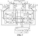
- FIG. 1 is a block diagram illustrating an example structure of a control device for a power converter according to this embodiment. First, an outline of the power system to which the control device for the power converter is applied will be described.
- the power system includes AC systems Aa, Ab, and a DC system D.
- the AC systems Aa and Ab are power systems that supply AC power, and the AC system Ab is a power transmitting side, while the AC system Ab is a power receiving side. In addition, both the AC systems Aa and Ab can be the power transmitting side or the power receiving side.
- the AC systems Aa and Ab each include facilities, such as a power supply, a load, and an AC lines.
- a transformer 1a is connected to the AC system Aa, and a transformer 1b is connected to the AC system Ab, respectively.
- the DC system D is a power system that supplies DC power, and has a one end connected to the AC system Aa via the transformer 1a. The other end is connected to the AC system Ab via the transformer 1b.
- the DC system D is provided with DC power transmission facilities.
- the transformers 1a and 1b are each a converter transformer that supplies a voltage to power converters 2a and 2b to be described later.
- the DC power transmission facilities establish a link between the AC systems Aa, Ab and the DC system D.
- the DC power transmission facilities include power converters 2a and 2b, DC lines 3a and 3b, DC reactors 4a and 4b, voltage detectors 5a and 5b, and current detectors 6a and 6b.
- the power converters 2a and 2b are each a separate-excitation type converter that utilizes a thyristor as a semiconductor device.
- the power converter 2a is connected to a control device Ca, and the power converter 2b is connected to a control device Cb.
- the power converter 2a is an AC-DC converter, and is connected to the AC system Aa via the transformer 1a.
- the power converter 2a converts AC power into DC power by turning ON the thyristor in accordance with a turn-ON signal from the control device Ca.
- the power converter 2b is an inverter, and is connected to the AC system Ab via the transformer 1b.
- the power converter 2b converts DC power into AC power by turning ON the thyristor in accordance with a turn-ON signal from the control device Cb.
- the power converter 2a can be an inverter
- the power converter 2b can be an AC-DC converter.
- the power converter 2a and the power converter 2b are connected to each other via the DC lines 3a and 3b.
- the DC reactor 4a is provided at the DC side of the power converter 2a in the DC line 3a.
- the DC reactor 4b is provided at the DC side of the power converter 2b in the DC line 3a.
- the DC reactors 4a and 4b are each a smoothing reactor which performs smoothing on a DC current and suppresses a DC eddy current. According to the above structure, the DC power converted by the power converter 2a is smoothed by the DC reactor 4a, is transmitted via the DC lines 3a and 3b, and is again smoothed by the DC reactor 4b, and eventually converted into AC power by the power converter 2b.
- the voltage detectors 5a and 5b are each a sensor that detects the DC voltage across both ends of the DC line 3a.
- the voltage detector 5a is provided between the end of the DC line 3a at the power-converter-2a side and the DC reactor 4a.
- a DC voltage Vd 1 detected by the voltage detector 5a is output to the control device Cb.
- the voltage detector 5b is provided between the end of the DC line 3a at the power-converter-2b side and the DC reactor 4b.
- a DC voltage Vd 2 detected by the voltage detector 5b is output to the control device Ca.
- the current detectors 6a and 6b are each a sensor that detects a DC current between both ends of the DC line 3a.
- the current detector 6a is provided between the end of the DC line 3a at the power-converter-2a side and the DC reactor 4a.
- a DC current Id 1 detected by the current detector 6a is output to the control device Ca.
- the current detector 6b is provided between the end of the DC line 3a at the power-converter-2b side and the DC reactor 4b.
- a DC current Id 2 detected by the current detector 6b is output to the control device Cb.
- control device Ca controls the power converter 2a, and includes a constant margin angle control circuit 10a, a constant voltage control circuit 11a, a constant current control circuit 12a, and a minimum value selecting circuit 13a.
- control device Cb controls the power converter 2b, and includes a constant margin angle control circuit 10b, a constant voltage control circuit 11b, a constant current control circuit 12b, and a minimum value selecting circuit 13b. That is, the power converters 2a and 2b basically employ the same structure.
- control device Ca includes adders 14a and 15a.
- control device Cb includes adders 14b, 15b, and 16b.
- Each adder is an arithmetic processing unit that adds a value input with a polarity indicated in FIG. 1 .
- the adder can also be considered as a subtractor.
- the constant margin angle control circuit 10a calculates a control angle that maintains a margin angle necessary for a commutation operation. Since the power converter 2a is a separate excitation type converter, when the margin angle for a converter decreases, a commutation failure is likely to occur. Hence, the constant margin angle control circuit 10a performs a control of ensuring the margin angle during the reverse converter operation, and suppressing a commutation failure of the converter. A control angle ⁇ 1A ⁇ R calculated by the constant margin angle control circuit 10a is output to the minimum value selecting circuit 13a.
- the constant voltage control circuit 11a performs a control of maintaining the DC voltage Vd 2 as constant. Input to the constant voltage control circuit 11a is a value obtained by adding the DC voltage Vd 2 detected by the voltage detector 5b and a predetermined DC voltage reference value Vdp by the adder 14a. The adder 14a calculates a difference of the DC voltage Vd 2 from the DC voltage reference value Vdp. The constant voltage control circuit 11a controls the DC voltage Vd 2 so as to be the value of the DC voltage reference value Vdp. A control angle ⁇ 1AVR calculated by the constant voltage control circuit 11a is output to the minimum value selecting circuit 13a.
- the constant current control circuit 12a performs a control of maintaining the DC current Id 1 as constant. Input to the constant current control circuit 12a is a value obtained by adding the DC current Id 1 detected by the current detector 6a and a predetermined DC current reference value Idp by the adder 15a. The adder 15a calculates a difference of the DC current reference value Idp from the DC current Id 1 . The constant current control circuit 12a controls the DC current Id 1 so as to be a value of the DC current reference value Idp. A control angle ⁇ 1ACR calculated by the constant current control circuit 12a is output to the minimum value selecting circuit 13a.
- the minimum value selecting circuit 13a compares, for example, multiple values, and determines the large-small relationship of the numerical values.
- the minimum value selecting circuit 13a selects the minimum value among the control angles input from the constant margin angle control circuit 10a, the constant voltage control circuit 11a, and the constant current control circuit 12a.
- An output ⁇ 1 by the minimum value selecting circuit 13a is a phase control angle for the gate pulse to the power converter 2a, and the power converter 2a is controlled based on this control angle.
- the constant margin angle control circuit 10b calculates a control angle for maintaining the margin angle necessary for a commutation operation. Since the power converter 2b is a separate excitation type converter, when the margin angle for the converter decreases, a commutation failure is likely to occur. Hence, the constant margin angle control circuit 10b performs a control of ensuring the margin angle during the reverse converter operation, and suppressing a commutation failure of the converter. A control angle ⁇ 2A ⁇ R calculated by the constant margin angle control circuit 10b is output to the minimum value selecting circuit 13b.
- the constant voltage control circuit 11b performs a control of maintaining the DC voltage Vd 1 as constant.
- Input to the constant voltage control circuit 11b is a value obtained by adding the DC voltage Vd 1 detected by the voltage detector 5a and the predetermined DC voltage reference value Vdp by the adder 14b.
- the adder 14b calculates a difference of the DC voltage Vd 1 from the DC voltage reference value Vdp.
- the constant voltage control circuit 11b controls the DC voltage Vd 1 so as to be the value of the DC voltage reference value Vdp.
- the control angle ⁇ 2AvR calculated by the constant voltage control circuit 11b is output to the adder 15b.
- An output ⁇ Id2 by an oscillation suppressing circuit 20 to be described later is also input to the adder 15b.
- the adder 15b adds the control angle ⁇ 2AvR of the constant voltage control circuit 11b and the output ⁇ Id2 of the oscillation suppressing circuit 20, and outputs the addition result to the minimum value selecting circuit 13b.
- the output ⁇ Id2 by the oscillation suppressing circuit 20 may be input to the adder 14b.
- the reverse characteristic of the constant voltage control circuit 11b i.e., the inverse of the transfer function of the constant voltage control circuit 11b may be applied, and the same characteristic as that of the case in which data is input the adder 15b may be achieved.
- the constant current control circuit 12b performs a control of maintaining the DC current Id 2 as constant.
- Input to the constant current control circuit 12b is a value obtained by adding the DC current Id 2 detected by the current detector 6b, the predetermined DC reference value Idp, and a current margin ⁇ Id by the adder 16b.
- the adder 16b adds the current margin ⁇ Id to a difference of the DC current Id 2 from the DC current reference value Idp.
- the constant current control circuit 12b controls the DC current Id 2 so as to be the value of the DC current reference value Idp.
- the control angle ⁇ 2ACR calculated by the constant current control circuit 12b is output to the minimum value selecting circuit 13b.
- the minimum value selecting circuit 13b compares, for example, multiple values, and determines the large-small relationship of the numerical values.
- the minimum value selecting circuit 13b selects the minimum value among the control angles input from the constant margin angle control circuit 10b, the adder 15b, and the constant current control circuit 12b.
- An output ⁇ 2 by this minimum value selecting circuit 13b is a phase control angle for the gate pulse to the power converter 2b, and the power converter 2b is controlled based on this phase control angle.
- the oscillation suppressing circuit 20 suppresses oscillation in the DC current, and includes an approximation differential value calculating circuit 21, and a filter circuit 22.
- the DC current Id 2 is input to the approximation differential value calculating circuit 21.
- the approximation differential value calculating circuit 21 calculates a differential value d(Id 2 )/dt of the DC current Id 2 .
- the calculated differential value d(Id 2 )/dt is input to the filter circuit 22.
- the filter circuit 22 allows only the frequency band within the predetermined range to pass.
- the filter circuit 22 is configured to cause the frequency band at which a suppression of an oscillation of the DC current Id 2 is desired to pass.
- the filter circuit 22 may be achieved by, for example, a circuit that includes a coil, a reactor, and a capacitor.
- the filter circuit 22 is applied to the input differential values d(Id 2 )/dt, and causes the differential value d(Id 2 )/dt of the frequency band at which a suppression of an oscillation of the DC current Id 2 is desired to pass.
- An output ⁇ Id 2 by the filter circuit 22 is output to the adder 15b.
- the adder 15b adds the outputs by the constant voltage control circuit 11b and the oscillation suppressing circuit 20, and outputs the addition result to the minimum value selecting circuit 13b.
- the AC system Aa is the transmitting side
- the AC system Ab is the power receiving side
- the power converter 2a operates as the Ac-DC converter
- the power converter 2b operates as the inverter.
- the control angle of the constant current control circuit 12a becomes smaller than the output by the constant margin angle control circuit 10a and that by the constant voltage control circuit 11a.
- the minimum value selecting circuit 13a outputs the control angle of the constant current control circuit 12a.
- the power converter 2a performs a constant current operation that maintains the DC current Id 1 as constant based on the control angle of the constant current control circuit 12a.
- the control angle of the constant voltage control circuit 11b becomes smaller than the output by the constant margin angle control circuit 10b and that by the constant current control circuit 12b.
- the differential value d (Id 2 ) /dt of the DC current Id 2 becomes substantially zero in the approximation differential value calculating circuit 21 of the oscillation suppressing circuit 20, the output ⁇ Id 2 by the filter circuit 22 also becomes substantially zero.
- the minimum value selecting circuit 13b outputs the control angle of the constant voltage control circuit 11b.
- the power converter 2b performs a constant voltage operation of maintaining the DC voltage Vd 1 as constant based on the control angle of the constant voltage control circuit 11b.
- V ac2 is a bus-line voltage of the AC system Ab
- X 2 is a reactance of the transformer 1b
- the control angle for the power converter 2b becomes ⁇ 2 > ⁇ /2.
- Vd 2 ⁇ 3 2 ⁇ V ac 2 cos ⁇ 2 ⁇ 3 ⁇ X 2 I d 2
- the output ⁇ Id2 by the oscillation suppressing circuit 20 becomes ⁇ Id2 > 0 when the oscillation waveform of the DC voltage Id 2 is increasing.
- the control angle ⁇ 2 in the formula 1 is increased, and this acts so as to increase the DC voltage Id 2 .
- the magnitude of the DC current Id 2 depends on the DC voltage Vd 1 - the DC voltage Vd 2 , the DC current Id 2 decreases when the DC voltage Vd 2 increases.
- the output ⁇ Id2 by the oscillation suppressing circuit 20 becomes ⁇ Id2 ⁇ 0 when the oscillation waveform of the DC current Id 2 is decreasing.
- the control angle ⁇ 2 in the formula 1 is decreased, and this acts so as to decrease the DC voltage Vd 2 , and increase the DC current Id 2 .
- the output ⁇ Id2 by the oscillation suppressing circuit 20 changes the DC current Id 2 so as to be decreased when the oscillation waveform is increasing, and to be increased when the oscillation waveform is decreasing. Therefore, oscillation is canceled by including the reverse phase component of the DC current Id 2 in the output by the constant voltage control circuit 11b.
- the structure of a control device for a power converter according to a second embodiment is basically the same as that of the first embodiment.
- the control angle ⁇ 1ACR calculated by the constant current control circuit 12a is output to the adder 16a.
- the output ⁇ Id2 ' by the oscillation suppressing circuit 20 to be described later is also input to the adder 16a.
- the adder 16a adds the control angle ⁇ 1ACR of the constant current control circuit 12a and the output ⁇ Id2 ' by the oscillation suppressing circuit 20, and outputs the addition result to the minimum value selecting circuit 13a.
- the output ⁇ Id2 ' by the oscillation suppressing circuit 20 may be input to the adder 15a.
- the reverse characteristic of the constant current control circuit 12a i.e., the inverse of the transfer function of the constant current control circuit 12a is applied, and the same characteristic as that of the case in which data is input to the adder 16a is achieved.
- the output by the oscillation suppressing circuit 20 of this embodiment is input to the control device Ca for the power converter 2a.
- the oscillation suppressing circuit 20 includes a DC circuit characteristic calculating circuit 23.
- the output ⁇ Id2 by the filter circuit 22 is input to the DC circuit characteristic calculating circuit 23.
- the DC circuit characteristic calculating circuit 23 is a filter circuit that has a characteristic which is a reverse characteristic of the transfer function from the DC voltage Vd 1 at the power-converter-2a side to the DC current Id 2 .
- the transfer function that indicates the characteristic at which the DC voltage Vd 1 acts on the DC current Id 2 will be described.
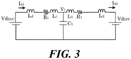
- FIG. 3 illustrates the equivalent circuit of the DC system D. The symbols in FIG. 3 indicate the following values.
- the following formula 3 indicates a transfer function that indicates the characteristic of the DC system D obtained by carrying out Laplace transformation on this formula 2, and arranging the transformation result.
- Id 1 P 11 s Vd REC + P 12 s Vd INV
- Id 2 P 21 s Vd REC + P 22 s Vd INV
- P 11 (s) is a transfer function to the DC current Id 1 from the DC voltage Vd REC
- P 12 (s) is a transfer function to the DC current Id 1 from the DC voltage Vd INV
- P 21 (s) is a transfer function to the DC current Id 2 from the DC voltage Vd REC
- P 22 (s) is a transfer function to the DC current Id 2 from the DC voltage Vd INV .
- V ac1 is a bus-line voltage of the AC system Aa
- X 1 is a reactance of the transformer 1a
- the control angle for the power converter 2a is ⁇ 1 ⁇ ⁇ /2.
- Vd 1 3 2 ⁇ V ac 1 cos ⁇ 1 ⁇ 3 ⁇ X 1 I d 1
- the DC circuit characteristic calculating circuit 23 reflects, on the differential value of the DC current Id 2 , the reverse characteristic P 21 (s) -1 of the influence of the DC voltage Vd REC on the DC current Id 2 .
- the output ⁇ Id2 ' by the DC circuit characteristic calculating circuit 23 is input to the adder 16a, and is added to the control angle ⁇ 1ACR of the constant current control circuit 12a.
- the control angle ⁇ 1 for the power converter 2a can be obtained from the control angle ⁇ 1ACR + the output ⁇ Id2 '.
- the output ⁇ Id2 ' by the oscillation suppressing circuit 20 compensates the characteristic of the DC circuit to the DC current Id 2 when the DC voltage Vd 1 is changed, when the oscillation waveform of the DC current Id 2 is increasing.
- the control angle ⁇ 1 in the formula 5 increases, and this acts so as to decrease the DC voltage Vd 1 and decrease the DC current Id 2 .
- the output ⁇ Id2 ' by the oscillation suppressing circuit 20 decreases the control angle ⁇ 1 when the oscillation waveform of the DC current Id 2 is decreasing, which acts so as to increase the DC voltage Vd 1 , and increase the DC current Id 2 .
- the DC circuit characteristic calculating circuit 23 puts the reverse-characteristic component of the transfer function to the DC current Id 2 from the DC voltage Vd 1 in the control angle ⁇ 1ACR of the constant current control circuit 12a, thereby canceling an oscillation of the DC current Id 2 .
- the structure of a control device for a power converter according to a third embodiment is basically the same as that of the first embodiment. As illustrated in FIG. 4 , however, in addition to the oscillation suppressing circuit 20, an ⁇ bias circuit 30 is provided.
- the ⁇ bias circuit 30 outputs a bias that decreases the control angle ⁇ 2 when the margin angle ⁇ is decreasing in addition to the DC current Id 2 .
- the ⁇ bias circuit 30 includes a ⁇ - ⁇ bias ' conversion circuit 31, an approximation differential value calculating circuit 32, and a primary delay circuit 33.
- the ⁇ - ⁇ bias ' conversion circuit 31 temporarily decreases the control angle ⁇ 2 when the DC current Id 2 oscillates and the margin angle ⁇ becomes equal to or smaller than a set value ⁇ min stored beforehand.
- the margin angle ⁇ of the power converter 2b is input to the ⁇ - ⁇ bias ' conversion circuit 31.
- the ⁇ - ⁇ bias ' conversion circuit 31 output ⁇ bias ' proportional to ⁇ min- ⁇ when ( ⁇ min- ⁇ ) becomes equal to or greater than a constant value.
- the output ⁇ bias ' by the ⁇ - ⁇ bias ' conversion circuit 31 is output to the approximation differential value calculating circuit 32.
- the approximation differential value calculating circuit 32 is an approximation differential value calculating circuit with a limiter which obtains a differential value d( ⁇ bias ')/dt of the output ⁇ bias ' by the ⁇ - ⁇ bias ' conversion circuit 31.
- the approximation differential value calculating circuit 32 outputs the differential value d( ⁇ bias ')/dt to the primary delay circuit 32 only when the differential value d( ⁇ bias ')/dt > 0 so as to detect only the increase in the output ⁇ bias ' by the ⁇ - ⁇ bias ' conversion circuit 31.
- the primary delay circuit 33 is a circuit that has the lower limiter which is the output d( ⁇ bias ')/dt by the approximation differential value calculating circuit 32.
- the primary delay circuit 33 has the output ⁇ bias gradually decreasing in accordance with a time constant T once d( ⁇ bias ') /dt > 0 even if d( ⁇ bias ') /dt decreases thereafter.
- the output ⁇ bias by the primary delay circuit 33 is output to a subtractor 24 of the oscillation suppressing circuit 20.
- the oscillation suppressing circuit 20 includes the subtractor 24.
- the subtractor 24 subtracts the output ⁇ bias by the ⁇ bias circuit 30 from the output ⁇ Id2 by the oscillation suppressing circuit 20.
- the output ⁇ Id2 ' by the oscillation suppressing circuit 20 is output to the constant margin angle control circuit 10b.
- the constant margin angle control circuit 10b includes adder 17b at the input side.
- the DC current Id 2 and the output ⁇ Id2 ' by the oscillation suppressing circuit 20 are input to the adder 17b and added by the adder.
- the adder 17b adds the DC current Id 2 and the output ⁇ Id2 ' by the oscillation suppressing circuit 20, and the constant margin angle control circuit 10b calculates the control angle using the output Id 2 '.
- the adder 17c may be utilized instead of the adder 17b to add the DC current Id 2 and the output ⁇ Id2 ' by the oscillation suppressing circuit 20.
- the oscillation suppressing circuit 20 stabilizes the DC current Id 2 of the power converter 2b that is operating under the constant margin angle control.
- the ⁇ bias circuit 30 prevents, by the oscillation suppressing circuit 20, the power converter 2b from failing commutation.
- the approximation differential value calculating circuit 21 outputs the differential value d(Id 2 )/dt of the DC current Id 2 .
- the filter circuit 22 applies, to the differential value d(Id 2 )/dt, the filter (e.g., bandpass filter) set beforehand for the frequency band at which a suppression of an oscillation of the DC current Id 2 is desired.
- the output ⁇ Id2 obtained by the filter circuit 22 is output to the constant margin angle control circuit 10b via the subtractor 24.
- the output ⁇ Id2 by the filter circuit 22 becomes ⁇ Id2 > 0 when the oscillation waveform of the DC voltage Id 2 is increasing.
- the control angle ⁇ 2 in the formula 1 increases, and this acts so as to increase the DC voltage Vd 2 .
- the output ⁇ Id2 by the filter circuit 22 becomes ⁇ Id2 ⁇ 0 when the oscillation waveform of the DC current Id 2 is decreasing.
- the control angle ⁇ 2 in the formula 1 is decreased, and this acts so as to decrease the DC voltage Vd 2 , and increase the DC current Id 2 .
- the output ⁇ Id2 by the filter circuit 22 increases the control angle ⁇ 2 when the DC voltage Id 2 is increasing. That is, since the control angle ⁇ 2 in the formula 1 becomes close to ⁇ , a commutation failure may occur the time of the constant margin angle control. Accordingly, when the DC current Id 2 oscillates and the margin angle ⁇ becomes equal to or smaller than the setting value, the ⁇ bias circuit 30 temporarily decreases ⁇ 2 , thereby preventing a commutation failure.
- the ⁇ - ⁇ bias ' conversion circuit 31 of the ⁇ bias circuit 30 outputs ⁇ bias ' proportional to ⁇ min- ⁇ when the margin angle ⁇ decreases and ( ⁇ min - ⁇ ) becomes equal to or greater than a certain value.
- the approximation differential value calculating circuit 32 outputs the differential value d( ⁇ bias ')/dt only when the differential value d( ⁇ bias ')/dt > 0, and detects only the increase in the output ⁇ bias ' by the ⁇ - ⁇ bias ' conversion circuit 31.
- the primary delay circuit 33 has the lower limit value that is the output d( ⁇ bias ') /dt by the differential value calculating circuit 32, and when d( ⁇ bias ')/dt > 0, gradually decreases the output ⁇ bias in accordance with the time constant T even if d( ⁇ bias ') /dt decreases.
- the ⁇ bias circuit 30 outputs ⁇ bias when the margin angle ⁇ is equal to or smaller than the certain value so as to act to prevent a commutation failure.
- the output by the approximation differential value calculating circuit 32 becomes d( ⁇ bias ')/dt ⁇ 0.
- the ⁇ bias circuit 30 does not act on the constant margin angle control circuit 10b in the stationary condition.
Landscapes
- Engineering & Computer Science (AREA)
- Power Engineering (AREA)
- Inverter Devices (AREA)
- Supply And Distribution Of Alternating Current (AREA)
- Direct Current Feeding And Distribution (AREA)
Abstract
Description
- Embodiments of the present disclosure relate to a control device for a power converter applied to, for example, DC power transmission.
- In DC power transmission facilities, two power converters are connected to respective AC systems via respective transformers. The two power converters configure an AC-DC converter and an inverter, respectively, and those are connected with each other via a DC reactor and a DC line. According to the above structure, AC power from one AC system is converted into DC power by the AC-DC converter, and is transmitted via the DC reactor and the DC line. The transmitted DC power is converted into AC power by the inverter.
- In DC power transmission, the current of a DC circuit for DC power transmission may oscillate due to control instability, etc. Hence, control devices for a power converter are provided with a circuit that suppresses an oscillation of a DC current. When, for example, the DC current at the AC-DC converter side oscillates due to a system fault, etc., the following scheme of cancelling the oscillation has been proposed; detecting the magnitude of the oscillation component and producing an oscillation of the DC current with an inverted phase relative to the oscillation of the input DC current by an oscillation suppressing circuit.
- Patent Document 1:
JP H09-046897 A - Non-Patent Document 1: Takehiko MACHIDA, "DC power transmission optics", the TOKYO DENKI University press, January 30, 1999, p. 151-154
- In recent years, along with the extension of the power transmission distance by DC power transmission, the power transmission cables which are DC lines are also extended. When a DC line is installed in ocean, in accordance with a power transmission distance, the electrostatic capacitance of a DC line increases. As described above, the DC circuit for DC power transmission includes a DC reactor and a DC line, etc. In this case, when the electrostatic capacitance of the DC line increases, the resonant frequency of the DC circuit due to the electrostatic capacitance of the DC reactor and that of the power transmission cable decreases. When this resonant frequency decreases down to around the frequency where a normal operation of the DC power transmission is operated, the DC current is affected by resonance, and may become oscillatory and unstable.
- According to conventional DC power transmission facilities, the DC current at the inverter side is not taken into consideration for control. Hence, when conventional power converters are applied to a long-distance power transmission, and the DC current keenly changes due to a system fault and a stepwise change in the DC current setting value, etc., a resonance of the DC circuit is induced, the DC current at the inverter side oscillates, possibly making the DC circuit unstable.
- Embodiments of the present disclosure have been proposed in order to address the foregoing problems of conventional technologies. The objective is to provide a control device for a power converter which promptly suppresses an oscillation when a DC current oscillates, and which stabilizes a DC power transmission.
- In order to accomplish the above objective, a control device according to an embodiment of the present disclosure is for a power converter that is an inverter converting DC power into AC power between two power converters connected with each other via a DC line, and the control device includes :
- a constant margin angle control circuit controlling so as to maintain a constant margin angle for the power converter;
- a constant voltage control circuit controlling so as to cause a DC voltage of the DC line to be a predetermined DC voltage reference value;
- a constant current control circuit controlling so as to cause a DC current of the DC line to be a predetermined DC current reference value;
- an oscillation suppressing circuit outputting a differential value of the DC current at the inverter side;
- an adder adding an output by the constant voltage control circuit and an output by the oscillation suppressing circuit; and
- a minimum value selecting circuit selecting a minimum value among an output by the constant margin angle control circuit, an output by the adder, and an output by the constant current control circuit, and setting the selection result as a control angle for the power converter.
-
-
FIG. 1 is a block diagram illustrating an example structure of a control device for a power converter according to a first embodiment; -
FIG. 2 is a block diagram illustrating an example structure of a control device for a power converter according to a second embodiment; -
FIG. 3 is a circuit diagram illustrating an equivalent circuit of a DC system; and -
FIG. 4 is a block diagram illustrating an example structure of a control device for a power converter according to a third embodiment. - A first embodiment according to the present disclosure will be described with reference to figures.
FIG. 1 is a block diagram illustrating an example structure of a control device for a power converter according to this embodiment. First, an outline of the power system to which the control device for the power converter is applied will be described. The power system includes AC systems Aa, Ab, and a DC system D. - The AC systems Aa and Ab are power systems that supply AC power, and the AC system Ab is a power transmitting side, while the AC system Ab is a power receiving side. In addition, both the AC systems Aa and Ab can be the power transmitting side or the power receiving side. The AC systems Aa and Ab each include facilities, such as a power supply, a load, and an AC lines. A
transformer 1a is connected to the AC system Aa, and atransformer 1b is connected to the AC system Ab, respectively. - The DC system D is a power system that supplies DC power, and has a one end connected to the AC system Aa via the
transformer 1a. The other end is connected to the AC system Ab via thetransformer 1b. The DC system D is provided with DC power transmission facilities. Thetransformers power converters - The DC power transmission facilities establish a link between the AC systems Aa, Ab and the DC system D. The DC power transmission facilities include
power converters DC lines DC reactors voltage detectors current detectors power converters power converter 2a is connected to a control device Ca, and thepower converter 2b is connected to a control device Cb. - The
power converter 2a is an AC-DC converter, and is connected to the AC system Aa via thetransformer 1a. Thepower converter 2a converts AC power into DC power by turning ON the thyristor in accordance with a turn-ON signal from the control device Ca. In addition, thepower converter 2b is an inverter, and is connected to the AC system Ab via thetransformer 1b. Thepower converter 2b converts DC power into AC power by turning ON the thyristor in accordance with a turn-ON signal from the control device Cb. When the flow of power is inverted, thepower converter 2a can be an inverter, and thepower converter 2b can be an AC-DC converter. - The
power converter 2a and thepower converter 2b are connected to each other via theDC lines DC reactor 4a is provided at the DC side of thepower converter 2a in theDC line 3a. TheDC reactor 4b is provided at the DC side of thepower converter 2b in theDC line 3a. TheDC reactors power converter 2a is smoothed by theDC reactor 4a, is transmitted via theDC lines DC reactor 4b, and eventually converted into AC power by thepower converter 2b. - The
voltage detectors DC line 3a. Thevoltage detector 5a is provided between the end of theDC line 3a at the power-converter-2a side and theDC reactor 4a. A DC voltage Vd1 detected by thevoltage detector 5a is output to the control device Cb. Thevoltage detector 5b is provided between the end of theDC line 3a at the power-converter-2b side and theDC reactor 4b. A DC voltage Vd2 detected by thevoltage detector 5b is output to the control device Ca. - The
current detectors DC line 3a. Thecurrent detector 6a is provided between the end of theDC line 3a at the power-converter-2a side and theDC reactor 4a. A DC current Id1 detected by thecurrent detector 6a is output to the control device Ca. Thecurrent detector 6b is provided between the end of theDC line 3a at the power-converter-2b side and theDC reactor 4b. A DC current Id2 detected by thecurrent detector 6b is output to the control device Cb. - Next, a structure of the control device Ca, Cb of the
power converter power converter 2a, and includes a constant marginangle control circuit 10a, a constantvoltage control circuit 11a, a constantcurrent control circuit 12a, and a minimumvalue selecting circuit 13a. The control device Cb controls thepower converter 2b, and includes a constant marginangle control circuit 10b, a constantvoltage control circuit 11b, a constantcurrent control circuit 12b, and a minimumvalue selecting circuit 13b. That is, thepower converters - In addition, the control device Ca includes
adders adders FIG. 1 . In addition, when the polarity is negative, the adder can also be considered as a subtractor. - The constant margin
angle control circuit 10a calculates a control angle that maintains a margin angle necessary for a commutation operation. Since thepower converter 2a is a separate excitation type converter, when the margin angle for a converter decreases, a commutation failure is likely to occur. Hence, the constant marginangle control circuit 10a performs a control of ensuring the margin angle during the reverse converter operation, and suppressing a commutation failure of the converter. A control angle α1AγR calculated by the constant marginangle control circuit 10a is output to the minimumvalue selecting circuit 13a. - The constant
voltage control circuit 11a performs a control of maintaining the DC voltage Vd2 as constant. Input to the constantvoltage control circuit 11a is a value obtained by adding the DC voltage Vd2 detected by thevoltage detector 5b and a predetermined DC voltage reference value Vdp by theadder 14a. Theadder 14a calculates a difference of the DC voltage Vd2 from the DC voltage reference value Vdp. The constantvoltage control circuit 11a controls the DC voltage Vd2 so as to be the value of the DC voltage reference value Vdp. A control angle α1AVR calculated by the constantvoltage control circuit 11a is output to the minimumvalue selecting circuit 13a. - The constant
current control circuit 12a performs a control of maintaining the DC current Id1 as constant. Input to the constantcurrent control circuit 12a is a value obtained by adding the DC current Id1 detected by thecurrent detector 6a and a predetermined DC current reference value Idp by theadder 15a. Theadder 15a calculates a difference of the DC current reference value Idp from the DC current Id1. The constantcurrent control circuit 12a controls the DC current Id1 so as to be a value of the DC current reference value Idp. A control angle α1ACR calculated by the constantcurrent control circuit 12a is output to the minimumvalue selecting circuit 13a. - The minimum
value selecting circuit 13a compares, for example, multiple values, and determines the large-small relationship of the numerical values. The minimumvalue selecting circuit 13a selects the minimum value among the control angles input from the constant marginangle control circuit 10a, the constantvoltage control circuit 11a, and the constantcurrent control circuit 12a. An output α1 by the minimumvalue selecting circuit 13a is a phase control angle for the gate pulse to thepower converter 2a, and thepower converter 2a is controlled based on this control angle. - The constant margin
angle control circuit 10b calculates a control angle for maintaining the margin angle necessary for a commutation operation. Since thepower converter 2b is a separate excitation type converter, when the margin angle for the converter decreases, a commutation failure is likely to occur. Hence, the constant marginangle control circuit 10b performs a control of ensuring the margin angle during the reverse converter operation, and suppressing a commutation failure of the converter. A control angle α2AγR calculated by the constant marginangle control circuit 10b is output to the minimumvalue selecting circuit 13b. - The constant
voltage control circuit 11b performs a control of maintaining the DC voltage Vd1 as constant. Input to the constantvoltage control circuit 11b is a value obtained by adding the DC voltage Vd1 detected by thevoltage detector 5a and the predetermined DC voltage reference value Vdp by theadder 14b. Theadder 14b calculates a difference of the DC voltage Vd1 from the DC voltage reference value Vdp. The constantvoltage control circuit 11b controls the DC voltage Vd1 so as to be the value of the DC voltage reference value Vdp. The control angle α2AvR calculated by the constantvoltage control circuit 11b is output to theadder 15b. An output ΔαId2 by anoscillation suppressing circuit 20 to be described later is also input to theadder 15b. Theadder 15b adds the control angle α2AvR of the constantvoltage control circuit 11b and the output ΔαId2 of theoscillation suppressing circuit 20, and outputs the addition result to the minimumvalue selecting circuit 13b. - The output ΔαId2 by the
oscillation suppressing circuit 20 may be input to theadder 14b. When theadder 14b is applied, the reverse characteristic of the constantvoltage control circuit 11b, i.e., the inverse of the transfer function of the constantvoltage control circuit 11b may be applied, and the same characteristic as that of the case in which data is input theadder 15b may be achieved. - The constant
current control circuit 12b performs a control of maintaining the DC current Id2 as constant. Input to the constantcurrent control circuit 12b is a value obtained by adding the DC current Id2 detected by thecurrent detector 6b, the predetermined DC reference value Idp, and a current margin ΔId by theadder 16b. Theadder 16b adds the current margin ΔId to a difference of the DC current Id2 from the DC current reference value Idp. The constantcurrent control circuit 12b controls the DC current Id2 so as to be the value of the DC current reference value Idp. The control angle α2ACR calculated by the constantcurrent control circuit 12b is output to the minimumvalue selecting circuit 13b. - The minimum
value selecting circuit 13b compares, for example, multiple values, and determines the large-small relationship of the numerical values. The minimumvalue selecting circuit 13b selects the minimum value among the control angles input from the constant marginangle control circuit 10b, theadder 15b, and the constantcurrent control circuit 12b. An output α2 by this minimumvalue selecting circuit 13b is a phase control angle for the gate pulse to thepower converter 2b, and thepower converter 2b is controlled based on this phase control angle. - The
oscillation suppressing circuit 20 suppresses oscillation in the DC current, and includes an approximation differentialvalue calculating circuit 21, and afilter circuit 22. The DC current Id2 is input to the approximation differentialvalue calculating circuit 21. The approximation differentialvalue calculating circuit 21 calculates a differential value d(Id2)/dt of the DC current Id2. The calculated differential value d(Id2)/dt is input to thefilter circuit 22. - The
filter circuit 22 allows only the frequency band within the predetermined range to pass. Thefilter circuit 22 is configured to cause the frequency band at which a suppression of an oscillation of the DC current Id2 is desired to pass. Thefilter circuit 22 may be achieved by, for example, a circuit that includes a coil, a reactor, and a capacitor. - The
filter circuit 22 is applied to the input differential values d(Id2)/dt, and causes the differential value d(Id2)/dt of the frequency band at which a suppression of an oscillation of the DC current Id2 is desired to pass. An output ΔαId2 by thefilter circuit 22 is output to theadder 15b. As described above, theadder 15b adds the outputs by the constantvoltage control circuit 11b and theoscillation suppressing circuit 20, and outputs the addition result to the minimumvalue selecting circuit 13b. - An operation of the control device for the power converter according to this embodiment will be described with reference to
FIG. 1 . - According to this embodiment, as described above, the AC system Aa is the transmitting side, and the AC system Ab is the power receiving side, the
power converter 2a operates as the Ac-DC converter, and thepower converter 2b operates as the inverter. In this case, in control device Ca, the control angle of the constantcurrent control circuit 12a becomes smaller than the output by the constant marginangle control circuit 10a and that by the constantvoltage control circuit 11a. Hence, the minimumvalue selecting circuit 13a outputs the control angle of the constantcurrent control circuit 12a. Thepower converter 2a performs a constant current operation that maintains the DC current Id1 as constant based on the control angle of the constantcurrent control circuit 12a. - In addition, in the control device Cb, when the AC voltage of the AC system Ab is near the rated value, the control angle of the constant
voltage control circuit 11b becomes smaller than the output by the constant marginangle control circuit 10b and that by the constantcurrent control circuit 12b. When there is no oscillation in the DC current Id2, since the differential value d (Id2) /dt of the DC current Id2 becomes substantially zero in the approximation differentialvalue calculating circuit 21 of theoscillation suppressing circuit 20, the output ΔαId2 by thefilter circuit 22 also becomes substantially zero. Hence, even if theadder 15b adds the output ΔαId2 by theoscillation suppressing circuit 20 to the output by thevoltage control circuit 11b, the value substantially remains unchanged. Accordingly, the minimumvalue selecting circuit 13b outputs the control angle of the constantvoltage control circuit 11b. Thepower converter 2b performs a constant voltage operation of maintaining the DC voltage Vd1 as constant based on the control angle of the constantvoltage control circuit 11b. - In contrast, when an oscillation occurs in the DC current Id2, since the differential value d(Id2)/dt becomes a value in accordance with the oscillation, the output ΔαId2 by the
oscillation suppressing circuit 20 is to be added to the output α2AVR by thevoltage control circuit 11b by theadder 15b. In this case, there is a relationship indicated by the followingformula 1 between the control angle α2 for thepower converter 2b obtained by adding the output ΔαId2 by theoscillation suppressing circuit 20 to the output α2AVR by thevoltage control circuit 11b, and the DC voltage Vd2 of thepower converter 2b. In theformula 1, Vac2 is a bus-line voltage of the AC system Ab, X2 is a reactance of thetransformer 1b, and the control angle for thepower converter 2b becomes α2 > π/2.
- The output ΔαId2 by the
oscillation suppressing circuit 20 becomes ΔαId2 > 0 when the oscillation waveform of the DC voltage Id2 is increasing. Hence, the control angle α2 in theformula 1 is increased, and this acts so as to increase the DC voltage Id2. In addition, since the magnitude of the DC current Id2 depends on the DC voltage Vd1 - the DC voltage Vd2, the DC current Id2 decreases when the DC voltage Vd2 increases. - In contrast, the output ΔαId2 by the
oscillation suppressing circuit 20 becomes ΔαId2 < 0 when the oscillation waveform of the DC current Id2 is decreasing. Hence, the control angle α2 in theformula 1 is decreased, and this acts so as to decrease the DC voltage Vd2, and increase the DC current Id2. As described above, the output ΔαId2 by theoscillation suppressing circuit 20 changes the DC current Id2 so as to be decreased when the oscillation waveform is increasing, and to be increased when the oscillation waveform is decreasing. Therefore, oscillation is canceled by including the reverse phase component of the DC current Id2 in the output by the constantvoltage control circuit 11b. - The action and effect of the above embodiment are as follows.
- (1) The control device Cb is for the
power converter 2b that is an inverter converting DC power into AC power between the twopower converters DC line 3a, and includes the constant marginangle control circuit 10b controlling so as to maintain the constant margin angle for thepower converter 2b, the constantvoltage control circuit 11b controlling so as to cause the DC voltage of theDC line 3a to be the predetermined DC voltage reference value, the constantcurrent control circuit 12b controlling so as to cause the DC current of theDC line 3a to be the predetermined DC current reference value, theoscillation suppressing circuit 20 outputting the differential value of the DC current at the inverter side, theadder 15b adding the output by the constantvoltage control circuit 11b and the output by theoscillation suppressing circuit 20, and the minimumvalue selecting circuit 12b selecting the minimum value among the output by the constant marginangle control circuit 10b, the output by theadder 15b, and the output by the constantcurrent control circuit 12b, and setting the selection result as the control angle for thepower converter 2b.
According to the above structure, the output ΔαId2 obtained by applying the approximation differentiation and the filter to the DC current Id2 at thepower converter 2b by theoscillation suppressing circuit 20, is applied to the output by the constantvoltage control circuit 11b. When the DC current Id2 oscillates, while thepower converter 2b performs the constant voltage control, the DC voltage Vd2 is changed so as to cause the DC current Id2 to oscillate reversely relative to the oscillation of the DC current Id2. That is, the reverse phase component by the change in the DC current Id2 is applied to the input of constant voltage control. Therefore, when the DC current Id2 oscillates, the oscillation is promptly suppressed, thereby stabilizing DC power transmission. - (2) The
oscillation suppressing circuit 20 includes the approximation differentialvalue calculating circuit 21 calculating the differential value of the DC current at the inverter side, and thefilter circuit 22 outputting the differential value of the frequency band at which a suppression of an oscillation is desired in the DC current at the inverter side. The differential value calculated by the approximation differentialvalue calculating circuit 21 is added to the constantvoltage control circuit 11b, and thus the damping performance increases, facilitating an oscillating to attenuate. - The structure of a control device for a power converter according to a second embodiment is basically the same as that of the first embodiment. According to the control device for the power converter of this embodiment, however, as illustrated in
FIG. 2 , in the control device Ca for thepower converter 2a, the control angle α1ACR calculated by the constantcurrent control circuit 12a is output to theadder 16a. The output ΔαId2' by theoscillation suppressing circuit 20 to be described later is also input to theadder 16a. Theadder 16a adds the control angle α1ACR of the constantcurrent control circuit 12a and the output ΔαId2' by theoscillation suppressing circuit 20, and outputs the addition result to the minimumvalue selecting circuit 13a. - The output ΔαId2' by the
oscillation suppressing circuit 20 may be input to theadder 15a. When theadder 15a is applied, the reverse characteristic of the constantcurrent control circuit 12a, i.e., the inverse of the transfer function of the constantcurrent control circuit 12a is applied, and the same characteristic as that of the case in which data is input to theadder 16a is achieved. - As described above, the output by the
oscillation suppressing circuit 20 of this embodiment is input to the control device Ca for thepower converter 2a. Theoscillation suppressing circuit 20 includes a DC circuit characteristic calculatingcircuit 23. The output ΔαId2 by thefilter circuit 22 is input to the DC circuit characteristic calculatingcircuit 23. - The DC circuit characteristic calculating
circuit 23 is a filter circuit that has a characteristic which is a reverse characteristic of the transfer function from the DC voltage Vd1 at the power-converter-2a side to the DC current Id2. First, the transfer function that indicates the characteristic at which the DC voltage Vd1 acts on the DC current Id2 will be described.FIG. 3 illustrates the equivalent circuit of the DC system D. The symbols inFIG. 3 indicate the following values. - VdREC: DC voltage Vd1 at the power-converter-2a side (AC-DC converter).
- VdINV: DC voltage Vd2 at the power-converter-2b side (inverter).
- Cl: Electrostatic capacitance value of the DC line.
- Rl: Resistance value of the DC line.
- Ll: Reactor value of the DC line.
- Ld: Reactor value of the DC reactor.
- Vl: Intermediate voltage of the DC line.
- The following
formula 2 indicates the mathematization of the DC system D based on this equivalent circuit.
- The following formula 3 indicates a transfer function that indicates the characteristic of the DC system D obtained by carrying out Laplace transformation on this
formula 2, and arranging the transformation result.
- In this case, P11(s) is a transfer function to the DC current Id1 from the DC voltage VdREC, P12 (s) is a transfer function to the DC current Id1 from the DC voltage VdINV, P21 (s) is a transfer function to the DC current Id2 from the DC voltage VdREC, and P22 (s) is a transfer function to the DC current Id2 from the DC voltage VdINV.
- In the above formula 3, when the DC voltage VdREC is changed, as for the action to the DC current Id2, it is apparent that the value obtained by multiplying the transfer function P21 (s) by VdREC acts. Hence, a change ΔVdREC of the DC voltage VdREC by the
oscillation suppressing circuit 20 is substituted in the formula 3 as ΔVdREC ≅ -P21 (s)-1 (ΔαId2), and the following formula is obtained.
- Based on the
above formula 4, when the characteristic of the DC circuit characteristic calculatingcircuit 23 is set to be P21 (s)-1 that is an inverse of the transfer function to the DC current Id2 from the DC voltage VdREC, it becomes apparent that the output ΔαId2 by thefilter circuit 22 can act on the DC current Id2 without affecting on the characteristic (P21(s)) of the DC circuit. - An operation of the control device for the power converter according to this embodiment will be described below. There is a relationship indicated in the following formula 5 between the control angle α1 and the DC voltage Vd1 for the
power converter 2a. In the formula 5, Vac1 is a bus-line voltage of the AC system Aa, X1 is a reactance of thetransformer 1a, and the control angle for thepower converter 2a is α1 < π/2.
- The DC circuit characteristic calculating
circuit 23 reflects, on the differential value of the DC current Id2, the reverse characteristic P21 (s)-1 of the influence of the DC voltage VdREC on the DC current Id2. The output ΔαId2' by the DC circuit characteristic calculatingcircuit 23 is input to theadder 16a, and is added to the control angle α1ACR of the constantcurrent control circuit 12a. Hence, the control angle α1 for thepower converter 2a can be obtained from the control angle α1ACR + the output ΔαId2'. - The output ΔαId2' by the
oscillation suppressing circuit 20 compensates the characteristic of the DC circuit to the DC current Id2 when the DC voltage Vd1 is changed, when the oscillation waveform of the DC current Id2 is increasing. Hence, the control angle α1 in the formula 5 increases, and this acts so as to decrease the DC voltage Vd1 and decrease the DC current Id2. - In contrast, the output ΔαId2' by the
oscillation suppressing circuit 20 decreases the control angle α1 when the oscillation waveform of the DC current Id2 is decreasing, which acts so as to increase the DC voltage Vd1, and increase the DC current Id2. As described above, the DC circuit characteristic calculatingcircuit 23 puts the reverse-characteristic component of the transfer function to the DC current Id2 from the DC voltage Vd1 in the control angle α1ACR of the constantcurrent control circuit 12a, thereby canceling an oscillation of the DC current Id2. - The action and effect of the above embodiment are as follows.
- (1) The control device Ca that is for the power converter controls an AC-DC converter converting AC power into DC power between the two power converters 2a and 2b connected with each other via the DC line 3a, and includes the constant margin angle control circuit 10a controlling so as to maintain the constant margin angle for the power converter 2a, the constant voltage control circuit 11a controlling so as to cause the DC voltage of the DC line to be the predetermined DC voltage reference value, the constant current control circuit 12a controlling so as to cause the DC current of the DC line 3a to be the predetermined DC current reference value, the oscillation suppressing circuit 21 outputting the differential value of the DC current at the inverter side, the filter circuit 22 outputting the differential value of the frequency band at which a suppression of an oscillation is desired, the DC circuit characteristic calculating circuit 23 reflecting, on the differential value, the reverse characteristic of the transfer function from the DC voltage at the AC-DC converter-2a side to the DC current at the inverter side, the adder 16a adding the output by the constant current control circuit 12a and the output by the DC circuit characteristic calculating circuit 23, and the minimum value selecting circuit selecting the minimum value among the output by the constant margin angle control circuit 10a, the output by the adder 16a, and the output by the constant voltage control circuit 11a, and setting the selection result as the control angle for the above power converter.
According to the above structure, the output ΔαId2 obtained by applying, to the DC current Id2 at thepower converter 2b, the approximation differentiation and the filter is outputted to the DC circuit characteristicsoperational circuit 23 by theoscillation suppressing circuit 20. In the DC circuit characteristic calculatingcircuit 23, the reverse characteristic of the transfer function from the DC voltage Vd1 to the DC current Id2 is reflected on the ΔαId2, and the output ΔαId2' is applied to the output by the constantcurrent control circuit 12a. When the DC current Id2 oscillates, while thepower converter 2a performs a constant current control, the DC voltage Vd1 is changed so as to cause the DC current Id2 to oscillate reversely relative to the oscillation of the DC current Id2. That is, the reverse phase component by what corresponds to a change in the DC current Id2 is applied to the input of the constant current control. Therefore, when the DC current Id2 oscillates, the oscillation is promptly suppressed, thereby stabilizing DC power transmission. - (2) The
oscillation suppressing circuit 20 includes the approximation differentialvalue calculating circuit 21 calculating the differential value of the DC current at the inverter side, thefilter circuit 22 outputting the differential value of the frequency band at which a suppression of an oscillation is desired in the DC current at the inverter side, and the DC circuit characteristic calculatingcircuit 23 reflecting the reverse characteristic of the transfer function from the DC voltage Vd1 to the DC current Id2. Addition of the output by theoscillation suppressing circuit 20 to the constantcurrent control circuit 12b improves the damping performance, facilitating an oscillation to attenuate. - The structure of a control device for a power converter according to a third embodiment is basically the same as that of the first embodiment. As illustrated in
FIG. 4 , however, in addition to theoscillation suppressing circuit 20, an αbias circuit 30 is provided. The αbias circuit 30 outputs a bias that decreases the control angle α2 when the margin angle γ is decreasing in addition to the DC current Id2. The αbias circuit 30 includes a γ-αbias'conversion circuit 31, an approximation differentialvalue calculating circuit 32, and aprimary delay circuit 33. - The γ-αbias'
conversion circuit 31 temporarily decreases the control angle α2 when the DC current Id2 oscillates and the margin angle γ becomes equal to or smaller than a set value γmin stored beforehand. The margin angle γ of thepower converter 2b is input to the γ-αbias'conversion circuit 31. The γ-αbias'conversion circuit 31 output αbias' proportional to γmin-γ when (γmin-γ) becomes equal to or greater than a constant value. The output αbias' by the γ-αbias'conversion circuit 31 is output to the approximation differentialvalue calculating circuit 32. - The approximation differential
value calculating circuit 32 is an approximation differential value calculating circuit with a limiter which obtains a differential value d(αbias')/dt of the output αbias' by the γ-αbias'conversion circuit 31. The approximation differentialvalue calculating circuit 32 outputs the differential value d(αbias')/dt to theprimary delay circuit 32 only when the differential value d(αbias')/dt > 0 so as to detect only the increase in the output αbias' by the γ-αbias'conversion circuit 31. - The
primary delay circuit 33 is a circuit that has the lower limiter which is the output d(αbias')/dt by the approximation differentialvalue calculating circuit 32. Theprimary delay circuit 33 has the output αbias gradually decreasing in accordance with a time constant T once d(αbias') /dt > 0 even if d(αbias') /dt decreases thereafter. The output αbias by theprimary delay circuit 33 is output to a subtractor 24 of theoscillation suppressing circuit 20. - In addition to the approximation differential
value calculating circuit 21 and thefilter circuit 22, theoscillation suppressing circuit 20 includes the subtractor 24. The subtractor 24 subtracts the output αbias by the αbias circuit 30 from the output ΔαId2 by theoscillation suppressing circuit 20. The output ΔαId2' by theoscillation suppressing circuit 20 is output to the constant marginangle control circuit 10b. - The constant margin
angle control circuit 10b includesadder 17b at the input side. The DC current Id2 and the output ΔαId2' by theoscillation suppressing circuit 20 are input to theadder 17b and added by the adder. Theadder 17b adds the DC current Id2 and the output ΔαId2' by theoscillation suppressing circuit 20, and the constant marginangle control circuit 10b calculates the control angle using the output Id2'. In addition, theadder 17c may be utilized instead of theadder 17b to add the DC current Id2 and the output ΔαId2' by theoscillation suppressing circuit 20. - An operation of the control device for the power converter according to this embodiment will be described below. When the system voltage of the AC system Ab to which the
power converter 2b that is a inverter is connected is lower than the normal voltage, the output a2AγR by the constant marginangle control circuit 10b becomes smaller than the output α2AVR by the constantvoltage control circuit 11b at the control device Cb for thepower converter 2b. Hence, the minimumvalue selecting circuit 13b outputs the output α2AγR by the constant marginangle control circuit 10b. Thepower converter 2b performs a constant margin angle control of maintaining the margin angle γ in the following formula 6 as constant.
- In this case, what is assumed is a case in which the DC current Id1 and the DC current Id2 keenly change due to a system failure, a stepwise change in the DC current setting value, etc., and the DC current Id1 and the DC current Id2 are affected by oscillation of the DC circuit, thus becoming oscillating. In this case, the
oscillation suppressing circuit 20 stabilizes the DC current Id2 of thepower converter 2b that is operating under the constant margin angle control. In addition, the αbias circuit 30 prevents, by theoscillation suppressing circuit 20, thepower converter 2b from failing commutation. - That is, in the
oscillation suppressing circuit 20, the approximation differentialvalue calculating circuit 21 outputs the differential value d(Id2)/dt of the DC current Id2. Thefilter circuit 22 applies, to the differential value d(Id2)/dt, the filter (e.g., bandpass filter) set beforehand for the frequency band at which a suppression of an oscillation of the DC current Id2 is desired. The output ΔαId2 obtained by thefilter circuit 22 is output to the constant marginangle control circuit 10b via the subtractor 24. - Like the above embodiment, the output ΔαId2 by the
filter circuit 22 becomes ΔαId2 > 0 when the oscillation waveform of the DC voltage Id2 is increasing. Hence, the control angle α2 in theformula 1 increases, and this acts so as to increase the DC voltage Vd2. In contrast, the output ΔαId2 by thefilter circuit 22 becomes ΔαId2 < 0 when the oscillation waveform of the DC current Id2 is decreasing. Hence, the control angle α2 in theformula 1 is decreased, and this acts so as to decrease the DC voltage Vd2, and increase the DC current Id2. - As is apparent from the foregoing, the output ΔαId2 by the
filter circuit 22 increases the control angle α2 when the DC voltage Id2 is increasing. That is, since the control angle α2 in theformula 1 becomes close to π, a commutation failure may occur the time of the constant margin angle control. Accordingly, when the DC current Id2 oscillates and the margin angle γ becomes equal to or smaller than the setting value, the αbias circuit 30 temporarily decreases α2, thereby preventing a commutation failure. - That is, in
FIG. 4 , the γ-αbias'conversion circuit 31 of the αbias circuit 30 outputs αbias' proportional to γmin-γ when the margin angle γ decreases and (γmin-γ) becomes equal to or greater than a certain value. The approximation differentialvalue calculating circuit 32 outputs the differential value d(αbias')/dt only when the differential value d(αbias')/dt > 0, and detects only the increase in the output αbias' by the γ-αbias'conversion circuit 31. - The
primary delay circuit 33 has the lower limit value that is the output d(αbias') /dt by the differentialvalue calculating circuit 32, and when d(αbias')/dt > 0, gradually decreases the output αbias in accordance with the time constant T even if d(αbias') /dt decreases. Hence, when the DC current Id2 oscillates and d(αbias')/dt > 0, the αbias circuit 30 outputs αbias when the margin angle γ is equal to or smaller than the certain value so as to act to prevent a commutation failure. - When the oscillation of the DC current Id2 is suppressed and the margin angle γ becomes unchanged, the output by the approximation differential
value calculating circuit 32 becomes d(αbias')/dt ≅ 0. In addition, the output by theprimary delay circuit 33 also gradually decreases depending on the time constant T, and becomes αbias = 0. Hence, the αbias circuit 30 does not act on the constant marginangle control circuit 10b in the stationary condition. - The action and effect of the above embodiment are as follows.
- (1) The control device Cb is for the
power converter 2b that is a inverter converting DC power into AC power between the twopower converters DC line 3a, and includes the constant marginangle control circuit 10b controlling so as to maintain the constant margin angle for thepower converter 2b, the constantvoltage control circuit 11b controlling so as to cause the DC voltage of theDC line 3a to be the predetermined DC voltage reference value, the constantcurrent control circuit 12b controlling so as to cause the DC current of theDC line 3a to be the predetermined DC current reference value, theoscillation suppressing circuit 20 outputting the differential value of the DC current at the inverter side, the αbias circuit 30 outputting the bias to the differential value, theadder 17b adding the output by theoscillation suppressing circuit 20, and the output by the αbias circuit 30 to the input side of the constant marginangle control circuit 10b, and the minimumvalue selecting circuit 13b selecting the minimum value among the output by the constant marginangle control circuit 10b, the output by the constantvoltage control circuit 11b, and the output by the constantcurrent control circuit 12b, and setting the selection result as the control angle for thepower converter 2b.
According to the above structure, the output ΔαId2 obtained by applying the approximation differentiation and the filter to the DC current Id2 at thepower converter 2b by theoscillation suppressing circuit 20 is applied to the output by the constantvoltage control circuit 11b. When the DC current Id2 oscillates, while thepower converter 2b performs a constant voltage control, the DC voltage Vd2 is changed so as to cause the DC current Id2 to oscillate reversely to the oscillation of the DC current Id2. That is, the reverse phase component by what corresponds to a change in the DC current Id2 is applied to the input of the constant voltage control. Therefore, when the DC current Id2 oscillates, the oscillation is promptly suppressed, thereby stabilizing DC power transmission.
In addition, the αbias circuit 30 detects a decrease in the margin angle γ and an oscillation, and has an offset value that temporarily decreases the control angle α2. This prevents the control angle α2 from increasing due to the output ΔαId2 by theoscillation suppressing circuit 20, thereby preventing thepower converter 2b from failing a commutation. - (2) The
oscillation suppressing circuit 20 includes the approximation differentialvalue calculating circuit 21 calculating the differential value of the DC current at the inverter side, and thefilter circuit 22 outputting the differential value of the frequency band at which a suppression of an oscillation is desired in the DC current at the inverter side. Addition of the differential value calculated by the approximation differentialvalue calculating circuit 21 to the constantvoltage control circuit 11b improves the damping performance, facilitating the oscillation to attenuate. -
- (1) In the above embodiments, the description has been given of a control device for a power converter, as for other forms, a program can be taken into consideration which causes a computer to execute the functions of the respective above circuits. That is, the control devices Ca and Cb can be accomplished by controlling a computer with a predetermined program or by a special purpose electronic circuit. The program in this case physically utilizes hardware of the computer, thereby accomplishing the process of each unit as described above. In addition, a method, a program, and a recording medium that records the program which execute the process of each unit are also the forms of the embodiment. Still further, how to set the range processed by hardware and the range processed by a software including a program is not limited to any particular form.
- (2) Although several embodiments of the present disclosure have been described, those embodiments are presented as examples and are not intended to limit the scope of the present disclosure. Those embodiments can be carried out in other various forms, and various omissions, replacements, and modifications can be made thereto without departing from the scope of the present disclosure. Such embodiments and modified forms thereof are within the scope of the present disclosure, and also within the scope of the invention as recited in appended claims and the equivalent range thereto.
-
- Aa, Ab AC system
- D DC system
- Ca, Cb Control device for power converter
- 1a, 1b Transformer
- 2a, 2b Power converter
- 3a, 3b DC line
- 4a, 4b DC reactor
- 5a, 5b Voltage detector
- 6a, 6b Current detector
- 10a, 10b Constant margin angle control circuit
- 11a, 11b Constant voltage control circuit
- 12a, 12b Constant current control circuit
- 13a, 13bMinimum value selecting circuit
- 14a, 14b, 15a, 15b, 16a, 16b, 17b, 17c, 24 Adder or subtractor
- 20 Oscillation suppressing circuit
- 21 Approximation differential value calculating circuit
- 22 Filter circuit
- 23 DC circuit characteristic calculating circuit
- 30 αbias circuit
- 31 γ-αbias' conversion circuit
- 32 Approximation differential value calculating circuit
- 33 Primary delay circuit
Claims (4)
- A control device for a power converter that is an inverter converting DC power into AC power between two power converters connected with each other via a DC line, the control device comprising:a constant margin angle control circuit controlling so as to maintain a constant margin angle for the power converter;a constant voltage control circuit controlling so as to cause a DC voltage of the DC line to be a predetermined DC voltage reference value;a constant current control circuit controlling so as to cause a DC current of the DC line to be a predetermined DC current reference value;an oscillation suppressing circuit outputting a differential value of the DC current at the inverter side;an adder adding an output by the constant voltage control circuit and an output by the oscillation suppressing circuit; anda minimum value selecting circuit selecting a minimum value among an output by the constant margin angle control circuit, an output by the adder, and an output by the constant current control circuit, and setting the selection result as a control angle for the power converter.
- A control device for a power converter that is an AC-DC converter converting AC power into DC power between two power converters connected with each other via a DC line, the control device comprising:a constant margin angle control circuit controlling so as to maintain a constant margin angle for the power converter;a constant voltage control circuit controlling so as to cause a DC voltage of the DC line to be a predetermined DC voltage reference value;a constant current control circuit controlling so as to cause a DC current of the DC line to be a predetermined DC current reference value;an oscillation suppressing circuit outputting a differential value of the DC current at an inverter side;a DC circuit characteristic calculating circuit reflecting, on the differential value, a reverse characteristic of a transfer function from the DC voltage at the AC-DC converter side to the DC current at the inverter side;an adder adding an output by the constant current control circuit and an output by the DC circuit characteristic calculating circuit; anda minimum value selecting circuit selecting a minimum value among an output by the constant margin angle control circuit, an output by the adder, and an output by the constant voltage control circuit, and setting the selection result as a control angle for the power converter.
- A control device for a power converter that is a inverter converting DC power into AC power between two power converters connected with each other via a DC line, the control device comprising:a constant margin angle control circuit controlling so as to maintain a constant margin angle for the power converter;a constant voltage control circuit controlling so as to cause a DC voltage of the DC line to be a predetermined DC voltage reference value;a constant current control circuit controlling so as to cause a DC current of the DC line to be a predetermined DC current reference value;an oscillation suppressing circuit outputting a differential value of the DC current at the inverter side;an αbias circuit outputting a bias to the differential value;an adder adding an output by the oscillation suppressing circuit, and an output by the αbias circuit to an input side of the constant margin angle control circuit; anda minimum value selecting circuit selecting a minimum value among an output by the constant margin angle control circuit, an output by the constant voltage control circuit, and an output by the constant current control circuit, and setting the selection result as a control angle for the power converter.
- The power-converter control device according to any one of claims 1 to 3, wherein the oscillation suppressing circuit comprises:an approximation differential value calculating circuit calculating the differential value of the DC current at the inverter side; anda filter circuit outputting the differential value of the frequency band at which a suppression of an oscillation is desired in the DC current at the inverter side.
Applications Claiming Priority (2)
| Application Number | Priority Date | Filing Date | Title |
|---|---|---|---|
| JP2015088148A JP2016208681A (en) | 2015-04-23 | 2015-04-23 | Control device for power converter |
| PCT/JP2016/053799 WO2016170822A1 (en) | 2015-04-23 | 2016-02-09 | Control device for power converter |
Publications (2)
| Publication Number | Publication Date |
|---|---|
| EP3288166A1 true EP3288166A1 (en) | 2018-02-28 |
| EP3288166A4 EP3288166A4 (en) | 2018-09-12 |
Family
ID=57143918
Family Applications (1)
| Application Number | Title | Priority Date | Filing Date |
|---|---|---|---|
| EP16782844.1A Withdrawn EP3288166A4 (en) | 2015-04-23 | 2016-02-09 | Control device for power converter |
Country Status (3)
| Country | Link |
|---|---|
| EP (1) | EP3288166A4 (en) |
| JP (1) | JP2016208681A (en) |
| WO (1) | WO2016170822A1 (en) |
Cited By (2)
| Publication number | Priority date | Publication date | Assignee | Title |
|---|---|---|---|---|
| CN108521138A (en) * | 2018-04-27 | 2018-09-11 | 武汉大学 | A kind of straight-flow system is to AC fault commutation failure entirety immunocompetence evaluation method |
| CN110187201A (en) * | 2019-04-24 | 2019-08-30 | 中国电力科学研究院有限公司 | Consider the direct-current commutation failure method of discrimination of alternating current-direct current interaction |
Families Citing this family (7)
| Publication number | Priority date | Publication date | Assignee | Title |
|---|---|---|---|---|
| CN106505592A (en) * | 2016-12-22 | 2017-03-15 | 北京四方继保自动化股份有限公司 | A kind of flexible direct current additional control method for suppressing sub-synchronous oscillation |
| CN107681683B (en) * | 2017-11-10 | 2020-05-19 | 浙江大学 | Alternating current-direct current receiving end power grid commutation failure fault prevention method based on parameterized Thevenin equivalence |
| JP6997605B2 (en) * | 2017-12-01 | 2022-01-17 | 東芝産業機器システム株式会社 | DC active filter, converter |
| CN109861263A (en) * | 2018-11-30 | 2019-06-07 | 中国电力科学研究院有限公司 | A method and system for reducing the risk of commutation failure of UHVDC non-faulty layers |
| CN110460086B (en) * | 2019-09-11 | 2021-01-12 | 郑州轻工业学院 | Additional control method for inhibiting hybrid multi-feed-in direct current commutation failure |
| CN111884206B (en) * | 2020-07-15 | 2021-09-17 | 山东大学 | Key line impedance adjusting method and system for inhibiting multi-direct-current commutation failure linkage |
| CN113394788B (en) * | 2021-06-15 | 2023-03-24 | 南方电网科学研究院有限责任公司 | Control method and device for AC/DC parallel two-region system |
Family Cites Families (8)
| Publication number | Priority date | Publication date | Assignee | Title |
|---|---|---|---|---|
| JPS58112475A (en) * | 1981-12-26 | 1983-07-04 | Tokyo Electric Power Co Inc:The | Starting system for ac/dc converter |
| JPS60235219A (en) * | 1984-05-08 | 1985-11-21 | Toshiba Corp | Control method of phase modifying equipment |
| JPS60249824A (en) * | 1984-05-24 | 1985-12-10 | 株式会社東芝 | Method of controlling ac/dc converter |
| JPH05207650A (en) * | 1992-01-23 | 1993-08-13 | Toshiba Corp | Controller for dc transmission system |
| JPH1014256A (en) * | 1996-06-27 | 1998-01-16 | Toshiba Corp | Power converter |
| JP2001197669A (en) * | 2000-01-07 | 2001-07-19 | Electric Power Dev Co Ltd | Control device of AC / DC converter |
| JP2016005374A (en) * | 2014-06-17 | 2016-01-12 | 株式会社東芝 | Control device for power converter |
| JP2016152733A (en) * | 2015-02-18 | 2016-08-22 | 株式会社東芝 | Control device for power converter |
-
2015
- 2015-04-23 JP JP2015088148A patent/JP2016208681A/en active Pending
-
2016
- 2016-02-09 WO PCT/JP2016/053799 patent/WO2016170822A1/en not_active Ceased
- 2016-02-09 EP EP16782844.1A patent/EP3288166A4/en not_active Withdrawn
Cited By (4)
| Publication number | Priority date | Publication date | Assignee | Title |
|---|---|---|---|---|
| CN108521138A (en) * | 2018-04-27 | 2018-09-11 | 武汉大学 | A kind of straight-flow system is to AC fault commutation failure entirety immunocompetence evaluation method |
| CN108521138B (en) * | 2018-04-27 | 2022-02-01 | 武汉大学 | Method for evaluating overall immunity of direct-current system to alternating-current fault commutation failure |
| CN110187201A (en) * | 2019-04-24 | 2019-08-30 | 中国电力科学研究院有限公司 | Consider the direct-current commutation failure method of discrimination of alternating current-direct current interaction |
| CN110187201B (en) * | 2019-04-24 | 2021-11-16 | 中国电力科学研究院有限公司 | Direct current commutation failure judgment method considering alternating current and direct current interaction |
Also Published As
| Publication number | Publication date |
|---|---|
| EP3288166A4 (en) | 2018-09-12 |
| JP2016208681A (en) | 2016-12-08 |
| WO2016170822A1 (en) | 2016-10-27 |
Similar Documents
| Publication | Publication Date | Title |
|---|---|---|
| EP3288166A1 (en) | Control device for power converter | |
| KR101706406B1 (en) | Controlling an inverter device of a high voltage dc system for supporting an ac system | |
| EP2051362B1 (en) | Inverter | |
| KR20130044351A (en) | Harmonic current suppression method and harmonic current suppression device of power conversion device | |
| JP2013034386A (en) | Inverter control apparatus and power conversion device | |
| US10938209B2 (en) | Fault ride-through circuit with variable frequency transformer and control method thereof | |
| KR102142288B1 (en) | System for controlling grid-connected apparatus for distributed generation | |
| US10008937B1 (en) | Apparatus for controlling DC link voltage in power cell of medium-voltage inverter | |
| JP4320228B2 (en) | Control device for self-excited converter | |
| EP3340459B1 (en) | Method for controlling inverter | |
| JP5378244B2 (en) | Power converter | |
| JP6658111B2 (en) | AC power supply device and control method thereof | |
| JP4779777B2 (en) | Flicker suppression device | |
| JP2005278224A (en) | Elevator controller | |
| JP7599894B2 (en) | Power Conversion Equipment | |
| JP2002044866A (en) | Series Compensator and Thyristor Controlled Series Capacitor Controller | |
| JP6747756B2 (en) | Power conversion system | |
| EP3160030A1 (en) | Power converter control device | |
| JPH11187573A (en) | Harmonic voltage detection circuit of voltage detection type active filter | |
| EP3379720B1 (en) | Method for controlling inverter | |
| JP6822110B2 (en) | Power converter and power conversion system | |
| JP2020156146A (en) | Power converter | |
| JP3312178B2 (en) | Control device for self-excited inverter | |
| JP3911601B2 (en) | Generator motor control device and power generation system using the same | |
| JP2016082760A (en) | Three-phase neutral point clamp type power conversion device |
Legal Events
| Date | Code | Title | Description |
|---|---|---|---|
| STAA | Information on the status of an ep patent application or granted ep patent |
Free format text: STATUS: THE INTERNATIONAL PUBLICATION HAS BEEN MADE |
|
| PUAI | Public reference made under article 153(3) epc to a published international application that has entered the european phase |
Free format text: ORIGINAL CODE: 0009012 |
|
| STAA | Information on the status of an ep patent application or granted ep patent |
Free format text: STATUS: REQUEST FOR EXAMINATION WAS MADE |
|
| 17P | Request for examination filed |
Effective date: 20171123 |
|
| AK | Designated contracting states |
Kind code of ref document: A1 Designated state(s): AL AT BE BG CH CY CZ DE DK EE ES FI FR GB GR HR HU IE IS IT LI LT LU LV MC MK MT NL NO PL PT RO RS SE SI SK SM TR |
|
| AX | Request for extension of the european patent |
Extension state: BA ME |
|
| DAV | Request for validation of the european patent (deleted) | ||
| DAX | Request for extension of the european patent (deleted) | ||
| A4 | Supplementary search report drawn up and despatched |
Effective date: 20180809 |
|
| RIC1 | Information provided on ipc code assigned before grant |
Ipc: H02M 5/42 20060101ALI20180804BHEP Ipc: H02M 7/48 20070101AFI20180804BHEP Ipc: H02M 7/72 20060101ALI20180804BHEP Ipc: H02J 3/36 20060101ALI20180804BHEP Ipc: H02J 1/02 20060101ALI20180804BHEP Ipc: H02J 1/00 20060101ALI20180804BHEP |
|
| STAA | Information on the status of an ep patent application or granted ep patent |
Free format text: STATUS: THE APPLICATION HAS BEEN WITHDRAWN |
|
| 18W | Application withdrawn |
Effective date: 20181116 |