EP3288072A1 - Fingerprint recognition module and preparation method therefor - Google Patents
Fingerprint recognition module and preparation method therefor Download PDFInfo
- Publication number
- EP3288072A1 EP3288072A1 EP16889672.8A EP16889672A EP3288072A1 EP 3288072 A1 EP3288072 A1 EP 3288072A1 EP 16889672 A EP16889672 A EP 16889672A EP 3288072 A1 EP3288072 A1 EP 3288072A1
- Authority
- EP
- European Patent Office
- Prior art keywords
- fingerprint identification
- filling material
- identification chip
- cover
- module
- Prior art date
- Legal status (The legal status is an assumption and is not a legal conclusion. Google has not performed a legal analysis and makes no representation as to the accuracy of the status listed.)
- Withdrawn
Links
Images



Classifications
-
- G—PHYSICS
- G06—COMPUTING OR CALCULATING; COUNTING
- G06V—IMAGE OR VIDEO RECOGNITION OR UNDERSTANDING
- G06V40/00—Recognition of biometric, human-related or animal-related patterns in image or video data
- G06V40/10—Human or animal bodies, e.g. vehicle occupants or pedestrians; Body parts, e.g. hands
- G06V40/12—Fingerprints or palmprints
- G06V40/13—Sensors therefor
- G06V40/1329—Protecting the fingerprint sensor against damage caused by the finger
-
- B—PERFORMING OPERATIONS; TRANSPORTING
- B32—LAYERED PRODUCTS
- B32B—LAYERED PRODUCTS, i.e. PRODUCTS BUILT-UP OF STRATA OF FLAT OR NON-FLAT, e.g. CELLULAR OR HONEYCOMB, FORM
- B32B37/00—Methods or apparatus for laminating, e.g. by curing or by ultrasonic bonding
- B32B37/12—Methods or apparatus for laminating, e.g. by curing or by ultrasonic bonding characterised by using adhesives
- B32B37/1284—Application of adhesive
-
- G—PHYSICS
- G06—COMPUTING OR CALCULATING; COUNTING
- G06V—IMAGE OR VIDEO RECOGNITION OR UNDERSTANDING
- G06V40/00—Recognition of biometric, human-related or animal-related patterns in image or video data
- G06V40/10—Human or animal bodies, e.g. vehicle occupants or pedestrians; Body parts, e.g. hands
- G06V40/12—Fingerprints or palmprints
- G06V40/13—Sensors therefor
- G06V40/1306—Sensors therefor non-optical, e.g. ultrasonic or capacitive sensing
-
- H—ELECTRICITY
- H10—SEMICONDUCTOR DEVICES; ELECTRIC SOLID-STATE DEVICES NOT OTHERWISE PROVIDED FOR
- H10W—GENERIC PACKAGES, INTERCONNECTIONS, CONNECTORS OR OTHER CONSTRUCTIONAL DETAILS OF DEVICES COVERED BY CLASS H10
- H10W72/00—Interconnections or connectors in packages
-
- H—ELECTRICITY
- H10—SEMICONDUCTOR DEVICES; ELECTRIC SOLID-STATE DEVICES NOT OTHERWISE PROVIDED FOR
- H10W—GENERIC PACKAGES, INTERCONNECTIONS, CONNECTORS OR OTHER CONSTRUCTIONAL DETAILS OF DEVICES COVERED BY CLASS H10
- H10W72/00—Interconnections or connectors in packages
- H10W72/50—Bond wires
-
- H—ELECTRICITY
- H10—SEMICONDUCTOR DEVICES; ELECTRIC SOLID-STATE DEVICES NOT OTHERWISE PROVIDED FOR
- H10W—GENERIC PACKAGES, INTERCONNECTIONS, CONNECTORS OR OTHER CONSTRUCTIONAL DETAILS OF DEVICES COVERED BY CLASS H10
- H10W95/00—Packaging processes not covered by the other groups of this subclass
-
- H—ELECTRICITY
- H10—SEMICONDUCTOR DEVICES; ELECTRIC SOLID-STATE DEVICES NOT OTHERWISE PROVIDED FOR
- H10W—GENERIC PACKAGES, INTERCONNECTIONS, CONNECTORS OR OTHER CONSTRUCTIONAL DETAILS OF DEVICES COVERED BY CLASS H10
- H10W99/00—Subject matter not provided for in other groups of this subclass
-
- B—PERFORMING OPERATIONS; TRANSPORTING
- B32—LAYERED PRODUCTS
- B32B—LAYERED PRODUCTS, i.e. PRODUCTS BUILT-UP OF STRATA OF FLAT OR NON-FLAT, e.g. CELLULAR OR HONEYCOMB, FORM
- B32B2305/00—Condition, form or state of the layers or laminate
- B32B2305/34—Inserts
- B32B2305/342—Chips
-
- B—PERFORMING OPERATIONS; TRANSPORTING
- B32—LAYERED PRODUCTS
- B32B—LAYERED PRODUCTS, i.e. PRODUCTS BUILT-UP OF STRATA OF FLAT OR NON-FLAT, e.g. CELLULAR OR HONEYCOMB, FORM
- B32B2305/00—Condition, form or state of the layers or laminate
- B32B2305/72—Cured, e.g. vulcanised, cross-linked
-
- B—PERFORMING OPERATIONS; TRANSPORTING
- B32—LAYERED PRODUCTS
- B32B—LAYERED PRODUCTS, i.e. PRODUCTS BUILT-UP OF STRATA OF FLAT OR NON-FLAT, e.g. CELLULAR OR HONEYCOMB, FORM
- B32B2457/00—Electrical equipment
-
- B—PERFORMING OPERATIONS; TRANSPORTING
- B32—LAYERED PRODUCTS
- B32B—LAYERED PRODUCTS, i.e. PRODUCTS BUILT-UP OF STRATA OF FLAT OR NON-FLAT, e.g. CELLULAR OR HONEYCOMB, FORM
- B32B37/00—Methods or apparatus for laminating, e.g. by curing or by ultrasonic bonding
- B32B37/0007—Methods or apparatus for laminating, e.g. by curing or by ultrasonic bonding involving treatment or provisions in order to avoid deformation or air inclusion, e.g. to improve surface quality
- B32B37/003—Methods or apparatus for laminating, e.g. by curing or by ultrasonic bonding involving treatment or provisions in order to avoid deformation or air inclusion, e.g. to improve surface quality to avoid air inclusion
-
- B—PERFORMING OPERATIONS; TRANSPORTING
- B32—LAYERED PRODUCTS
- B32B—LAYERED PRODUCTS, i.e. PRODUCTS BUILT-UP OF STRATA OF FLAT OR NON-FLAT, e.g. CELLULAR OR HONEYCOMB, FORM
- B32B37/00—Methods or apparatus for laminating, e.g. by curing or by ultrasonic bonding
- B32B37/06—Methods or apparatus for laminating, e.g. by curing or by ultrasonic bonding characterised by the heating method
-
- B—PERFORMING OPERATIONS; TRANSPORTING
- B32—LAYERED PRODUCTS
- B32B—LAYERED PRODUCTS, i.e. PRODUCTS BUILT-UP OF STRATA OF FLAT OR NON-FLAT, e.g. CELLULAR OR HONEYCOMB, FORM
- B32B37/00—Methods or apparatus for laminating, e.g. by curing or by ultrasonic bonding
- B32B37/10—Methods or apparatus for laminating, e.g. by curing or by ultrasonic bonding characterised by the pressing technique, e.g. using action of vacuum or fluid pressure
-
- B—PERFORMING OPERATIONS; TRANSPORTING
- B32—LAYERED PRODUCTS
- B32B—LAYERED PRODUCTS, i.e. PRODUCTS BUILT-UP OF STRATA OF FLAT OR NON-FLAT, e.g. CELLULAR OR HONEYCOMB, FORM
- B32B38/00—Ancillary operations in connection with laminating processes
- B32B38/0004—Cutting, tearing or severing, e.g. bursting; Cutter details
-
- H—ELECTRICITY
- H10—SEMICONDUCTOR DEVICES; ELECTRIC SOLID-STATE DEVICES NOT OTHERWISE PROVIDED FOR
- H10W—GENERIC PACKAGES, INTERCONNECTIONS, CONNECTORS OR OTHER CONSTRUCTIONAL DETAILS OF DEVICES COVERED BY CLASS H10
- H10W72/00—Interconnections or connectors in packages
- H10W72/50—Bond wires
- H10W72/551—Materials of bond wires
- H10W72/552—Materials of bond wires comprising metals or metalloids, e.g. silver
- H10W72/5522—Materials of bond wires comprising metals or metalloids, e.g. silver comprising gold [Au]
-
- H—ELECTRICITY
- H10—SEMICONDUCTOR DEVICES; ELECTRIC SOLID-STATE DEVICES NOT OTHERWISE PROVIDED FOR
- H10W—GENERIC PACKAGES, INTERCONNECTIONS, CONNECTORS OR OTHER CONSTRUCTIONAL DETAILS OF DEVICES COVERED BY CLASS H10
- H10W74/00—Encapsulations, e.g. protective coatings
-
- H—ELECTRICITY
- H10—SEMICONDUCTOR DEVICES; ELECTRIC SOLID-STATE DEVICES NOT OTHERWISE PROVIDED FOR
- H10W—GENERIC PACKAGES, INTERCONNECTIONS, CONNECTORS OR OTHER CONSTRUCTIONAL DETAILS OF DEVICES COVERED BY CLASS H10
- H10W74/00—Encapsulations, e.g. protective coatings
- H10W74/10—Encapsulations, e.g. protective coatings characterised by their shape or disposition
- H10W74/111—Encapsulations, e.g. protective coatings characterised by their shape or disposition the semiconductor body being completely enclosed
- H10W74/114—Encapsulations, e.g. protective coatings characterised by their shape or disposition the semiconductor body being completely enclosed by a substrate and the encapsulations
-
- H—ELECTRICITY
- H10—SEMICONDUCTOR DEVICES; ELECTRIC SOLID-STATE DEVICES NOT OTHERWISE PROVIDED FOR
- H10W—GENERIC PACKAGES, INTERCONNECTIONS, CONNECTORS OR OTHER CONSTRUCTIONAL DETAILS OF DEVICES COVERED BY CLASS H10
- H10W90/00—Package configurations
- H10W90/701—Package configurations characterised by the relative positions of pads or connectors relative to package parts
- H10W90/751—Package configurations characterised by the relative positions of pads or connectors relative to package parts of bond wires
- H10W90/754—Package configurations characterised by the relative positions of pads or connectors relative to package parts of bond wires between a chip and a stacked insulating package substrate, interposer or RDL
Definitions
- the present disclosure relates to the technical filed of fingerprint identification, and in particular, relates to a fingerprint identification module and a method for manufacturing the same.
- the manufacture of a fingerprint identification module includes at least the following three processes:
- a fingerprint identification chip 100 is firstly soldered to a flexible printed circuit (FPC) 300 by using the surface mount technology (SMT).
- SMT surface mount technology
- a metal ring 400 is subsequently attached to the FPC 300.
- a glass cover 500 is finally attached on the surface of the fingerprint identification chip 100.
- such a manufacture process causes the attachment of the glass cover 500 and the fingerprint identification chip 100 to be simply subject to influences of the metal ring and the FPC, causes bubbles to be remained between the glass cover 500 and the fingerprint identification chip 100, and further affects the entire performance of the fingerprint identification module.
- such a manufacture process imposes a high requirement on an operation precision of the soldering and attachment, which objectively affects the efficiency of the production.
- a Chinese patent application titled "FINGERPRINT IDENTIFICATION MODULE AND METHOD FOR MANUFACTURING THE SAME, AND ELECTRONIC DEVICE HAVING THE FINGERPRINT IDENTIFICATION MODULE" discloses a fingerprint identification module, a method for manufacturing the same, and an electronic device having the same.
- the fingerprint identification module includes a laminated structure and a support element.
- the support element wraps the laminated structure; and the laminated structure includes a cover, a fingerprint identification chip disposed under the cover, a FPC disposed under the fingerprint identification chip and electrically connected to the fingerprint identification chip, and a reinforcement plate disposed under the FPC.
- An attach surface of the fingerprint identification module features flatness, smoothness and good tactility during the touch, and the sensing effect of the fingerprint identification chip may be better.
- the manufacturing method includes the following steps: (1) placing in a mould the laminated structure in which the reinforcement plate, the FPC, the fingerprint identification chip and the cover are disposed from bottom to top; and
- this fingerprint identification module has a compact structure, and a high integration.
- the laminated structure of the fingerprint identification module is relatively complex, and according to the manufacturing method, the bubbles are easily remained between the glass cover 500 and the fingerprint identification chip 100. Therefore, the entire performance of the fingerprint identification module may be affected.
- a fingerprint identification module and a method for manufacturing the same employ the following technical solutions.
- a fingerprint identification module is provided.
- the fingerprint identification module is obtained by dicing a board-level module, and includes a fingerprint identification chip, a filling material, a color coating and a cover.
- the color coating is disposed between the filling material and the cover, and the fingerprint identification chip is inversely attached in a hollow area of the filling material in a vacuum environment.
- the fingerprint identification chip includes an identification area, an interconnection gold thread, a molding layer, a substrate layer and a pad.
- the identification area is disposed inside of the molding layer, the substrate layer is adhered to the molding layer, the pad is disposed on an upper surface and a lower surface of the substrate layer and is further disposed on an upper surface of the identification area, and the pad on the upper surface of the identification area is connected to the pad on the upper surface of the substrate layer via the interconnection gold thread.
- an upper surface of the inversely-attached fingerprint identification chip is above an upper surface of the filling material.
- the filling material is an organic colloid, a film or a plastic, and has a photo-induced effect.
- the hollow area is obtained by exposing and developing a part of the filling material.
- the cover is a strip-type glass, a strip-type ceramic, a substrate-type glass, a substrate-type ceramic, or a disc-type glass having the same shape as a wafer.
- a method for manufacturing a fingerprint identification module includes:
- the attaching a fingerprint identification chip into each hollow area in the array of hollow areas of the filling material includes:
- an upper surface of the inversely-placed fingerprint identification chip is above an upper surface of the filling material.
- the filling material is an organic colloid, a film or a plastic, and has a photo-induced effect; and each hollow area in the array of hollow areas of the filling material is obtained by exposing and developing the filling material.
- the cover is a strip-type glass, a strip-type ceramic, a substrate-type glass, a substrate-type ceramic, or a disc-type glass having the same shape as a wafer.
- Reference numerals and denotations thereof 100-fingerprint identification chip, 101-identification area, 102-interconnection gold thread, 103-molding layer, 104-substrate layer, 105-pad, 200-fingerprint identification module, 201-filling material, 202-color coating, 203-cover, 204-glue layer, 300-flexible printed circuit, 400-metal ring, and 500-glass cover.
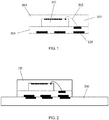
- a fingerprint identification chip 100 included in a fingerprint identification module includes an identification area 101, an interconnection gold thread 102, a molding layer 103, a substrate layer 104 and a pad 105.
- the identification area 101 is disposed inside of the molding layer 103, the substrate layer 104 is adhered to the molding layer 103, the pad 105 is disposed on an upper surface and a lower surface of the substrate layer 104 and is further disposed on an upper surface of the identification area 101, and the pad 105 on the upper surface of the identification area 101 is connected to the pad 105 on the upper surface of the substrate layer 104 via the interconnection gold thread 102.
- a fingerprint identification module provided in the embodiments of the present disclosure includes a fingerprint identification chip 100, a filling material 201, a color coating 202, a cover 203 and a glue layer 204.
- the color coating 202 is disposed between the filling material 201 and the cover 203, and the fingerprint identification chip 100 is inversely attached in a hollow area of the filling material 201 in a vacuum environment.
- the filling material 201 is a material having a photo-induced effect such as an organic colloid, a film or a plastic.
- the hollow area is obtained by exposing and developing a part of the filling material 201.
- the hollow area is filled with the glue layer 204, which is configured to attach the fingerprint identification chip 100.
- the fingerprint identification module is manufactured in batches on a board-level module, and is subsequently obtained via dicing. The structure is simple and easy to manufacture.
- a method for manufacturing for a fingerprint identification module provided in the embodiments of the present disclosure includes the following steps.
- Step S1 A board-level module is manufactured by using a filling material 201, a color coating 202 and a cover 203.
- the cover 203 is used as a carrier, and may use such materials as a strip-type glass, a strip-type ceramic, a substrate-type glass, a substrate-type ceramic, or a disc-type glass having the same shape as a wafer. Different sizes may be selected for the cover 203 according to the features of the industry or the wafer level module technology.
- the color coating 202 may be coated on the cover 203 by using such processes as silk screening, and a specific color may be customized according to customer's needs.
- the filling material 201 is coated on the color coating 202, the filling material 201 may be a material having a photo-induced effect such as an organic colloid, a film or a plastic, and the thickness of the filling material is customized according to the thickness of the fingerprint identification chip 100.
- Step S2 An array of hollow areas in a predetermined quantity is processed on the filling material 201 of the board-level module.
- the hollow area may be acquired by a photolithography process such as, exposing and developing the filling material 201. After the filling material 201 is hollowed, the size of each hollow area is a little bit greater than that of the fingerprint identification chip 100, and the filling material 201 may surround and support the fingerprint identification chip 100, and thus protect the fingerprint identification chip 100.
- a plurality of hollow area arrays may be manufactured on the filling material 201 of the same board-level module for manufacturing of the fingerprint identification module, such that the materials and processes are reduced, and the production efficiency is improved.
- Step S3 The fingerprint identification chip 100 is attached into each hollow area in the array of hollow areas of the filling material in a vacuum environment.
- step S3 the attaching a fingerprint identification chip 100 into each hollow area in the array of hollow areas of the filling material 201 includes the following steps.
- a glue with a preset thickness is uniformly filled at a bottom of each of the hollow areas, and a defoaming process is performed for the glue.
- each of the hollow areas is coated by the glue layer 204, such that the glue with a suitable thickness is uniformly filled at the bottom of the hollow area.
- the defoaming process is performed for the glue layer 204 to eliminate the bubbles.
- the fingerprint identification chip 100 is inversely placed in each hollow area in the array of hollow areas of the filling material 201.
- the manufactured board-level module is placed in a vacuum environment, and the atmospheric environment that exists in the hollow area is cleared.
- the fingerprint identification chip 100 is inversely placed in the hollow area, and an upper surface of the inversely-placed fingerprint identification chip 100 is above an upper surface of the filling material 201.
- S33 The fingerprint identification chip 100 is pressurized and heated, such that the fingerprint identification chip 100 is tightly attached to the glue and the glue is solidified.
- the fingerprint identification chip 100 in the vacuum environment, when being attached, the fingerprint identification chip 100 may be suitably pressurized and heated, such that the glue layer 204 is solidified, and the bubbles between the fingerprint identification chip 100 and the cover 203 may be greatly eliminated.
- Step S4 The board-level module is diced to obtain fingerprint identification modules.
- the size of the cover 203 may be 8 inches, 12 inches, or bigger, hundreds of hollow areas may be formed at one time on a corresponding board-level module.
- a plurality of fingerprint identification modules may be manufactured on the board-level module.
- the plurality of fingerprint identification modules on the same board-level module may be diced, such that a plurality of attached fingerprint identification modules may be obtained, which improves the production efficiency, and facilitates large-scale mass production.
- the foregoing method for manufacturing the fingerprint identification module is not limited to manufacturing the fingerprint identification module of the present disclosure.
Landscapes
- Engineering & Computer Science (AREA)
- Physics & Mathematics (AREA)
- Human Computer Interaction (AREA)
- General Physics & Mathematics (AREA)
- Multimedia (AREA)
- Theoretical Computer Science (AREA)
- Quality & Reliability (AREA)
- Fluid Mechanics (AREA)
- Measurement Of The Respiration, Hearing Ability, Form, And Blood Characteristics Of Living Organisms (AREA)
- Dicing (AREA)
- Image Input (AREA)
Abstract
Description
- The present disclosure relates to the technical filed of fingerprint identification, and in particular, relates to a fingerprint identification module and a method for manufacturing the same.
- In the prior art, the manufacture of a fingerprint identification module includes at least the following three processes:
- Referring to
FIG. 2 , afingerprint identification chip 100 is firstly soldered to a flexible printed circuit (FPC) 300 by using the surface mount technology (SMT). Referring toFIG. 3 , ametal ring 400 is subsequently attached to the FPC 300. Referring toFIG. 4 , aglass cover 500 is finally attached on the surface of thefingerprint identification chip 100. - Referring to
FIG. 4 , such a manufacture process causes the attachment of theglass cover 500 and thefingerprint identification chip 100 to be simply subject to influences of the metal ring and the FPC, causes bubbles to be remained between theglass cover 500 and thefingerprint identification chip 100, and further affects the entire performance of the fingerprint identification module. In addition, such a manufacture process imposes a high requirement on an operation precision of the soldering and attachment, which objectively affects the efficiency of the production. - A Chinese patent application titled "FINGERPRINT IDENTIFICATION MODULE AND METHOD FOR MANUFACTURING THE SAME, AND ELECTRONIC DEVICE HAVING THE FINGERPRINT IDENTIFICATION MODULE" (publication No.
CN 105046244 A ) discloses a fingerprint identification module, a method for manufacturing the same, and an electronic device having the same. The fingerprint identification module includes a laminated structure and a support element. The support element wraps the laminated structure; and the laminated structure includes a cover, a fingerprint identification chip disposed under the cover, a FPC disposed under the fingerprint identification chip and electrically connected to the fingerprint identification chip, and a reinforcement plate disposed under the FPC. An attach surface of the fingerprint identification module features flatness, smoothness and good tactility during the touch, and the sensing effect of the fingerprint identification chip may be better. - The manufacturing method includes the following steps: (1) placing in a mould the laminated structure in which the reinforcement plate, the FPC, the fingerprint identification chip and the cover are disposed from bottom to top; and
- (2) injecting a glue into the mould to enable the glue to wrap the laminated structure, solidifying the glue to form the support element, and subsequently demoulding, such that the fingerprint identification module is obtained; where the fingerprint identification chip is electrically connected to the FPC. By using this method, the fingerprint identification module having a smooth attach surface may be quickly and effectively manufactured, and the transmission effect of signals of the acquired fingerprint identification module is good, which effectively reduces electromagnetic filed loss caused by a rough attach surface, and improves the transmission effect of signals is improved. In addition, the support element is formed via injecting the glue and solidifying the glue, which effectively reduces the thickness of the fingerprint identification module. Further, by using the method for manufacturing the fingerprint identification module according to the embodiments of the present disclosure, the grinding is not required, the operation steps are simplified, and manpower and material resources are saved.
- To sum up, this fingerprint identification module has a compact structure, and a high integration. However, the laminated structure of the fingerprint identification module is relatively complex, and according to the manufacturing method, the bubbles are easily remained between the
glass cover 500 and thefingerprint identification chip 100. Therefore, the entire performance of the fingerprint identification module may be affected. - To effectively eliminate bubbles between a fingerprint identification chip and a cover, and improve the manufacture efficiency of fingerprint identification modules, a fingerprint identification module and a method for manufacturing the same according to the present disclosure employ the following technical solutions.
- A fingerprint identification module is provided. The fingerprint identification module is obtained by dicing a board-level module, and includes a fingerprint identification chip, a filling material, a color coating and a cover.
- The color coating is disposed between the filling material and the cover, and the fingerprint identification chip is inversely attached in a hollow area of the filling material in a vacuum environment.
- Further, the fingerprint identification chip includes an identification area, an interconnection gold thread, a molding layer, a substrate layer and a pad.
- The identification area is disposed inside of the molding layer, the substrate layer is adhered to the molding layer, the pad is disposed on an upper surface and a lower surface of the substrate layer and is further disposed on an upper surface of the identification area, and the pad on the upper surface of the identification area is connected to the pad on the upper surface of the substrate layer via the interconnection gold thread.
- Further, an upper surface of the inversely-attached fingerprint identification chip is above an upper surface of the filling material.
- Further, the filling material is an organic colloid, a film or a plastic, and has a photo-induced effect.
- The hollow area is obtained by exposing and developing a part of the filling material. Further, the cover is a strip-type glass, a strip-type ceramic, a substrate-type glass, a substrate-type ceramic, or a disc-type glass having the same shape as a wafer.
- A method for manufacturing a fingerprint identification module is provided. The method includes:
- manufacturing a board-level module using a filling material, a color coating and a cover, and processing an array of hollow areas in a predetermined quantity on the filling material of the board-level module;
- attaching a fingerprint identification chip into each hollow area in the array of hollow areas of the filling material in a vacuum environment; and
- dicing the board-level module to obtain fingerprint identification modules.
- Further, the attaching a fingerprint identification chip into each hollow area in the array of hollow areas of the filling material includes:
- uniformly filling a glue with a preset thickness at a bottom of each of the hollow areas, and performing a defoaming process for the glue;
- inversely placing the fingerprint identification chip in each hollow area in the array of hollow areas of the filling material; and
- pressurizing the fingerprint identification chip and heating to cure the fingerprint identification chip, such that the fingerprint identification chip is tightly attached to the glue and the glue is solidified.
- Further, an upper surface of the inversely-placed fingerprint identification chip is above an upper surface of the filling material.
- Further, the filling material is an organic colloid, a film or a plastic, and has a photo-induced effect; and
each hollow area in the array of hollow areas of the filling material is obtained by exposing and developing the filling material. - Further, the cover is a strip-type glass, a strip-type ceramic, a substrate-type glass, a substrate-type ceramic, or a disc-type glass having the same shape as a wafer.
- Compared with the prior art, the present disclosure has the following beneficial effects:
- 1. The fingerprint identification module according to the embodiments of the present disclosure is obtained by dicing a board-level module, and includes a fingerprint identification chip, a filling material, a color coating and a cover. The color coating is disposed between the filling material and the cover, and the fingerprint identification chip is inversely attached in a hollow area of the filling material in a vacuum environment. This fingerprint identification module has a simple structure, and is easy to manufacture.
- 2. The method for manufacturing the fingerprint identification module according to the embodiments of the present disclosure includes the following steps: manufacturing a board-level module using a filling material, a color coating and a cover, where the filling material includes an array of hollow areas; respectively attaching a plurality of fingerprint identification chips into each hollow area in the array of hollow areas of the filling material in a vacuum environment; and dicing the board-level module to obtain a plurality of fingerprint identification modules. The method effectively eliminates bubbles between the fingerprint identification chip and the cover, and improves the manufacture efficiency of the fingerprint identification module.
-
-
FIG. 1 is a schematic structural diagram of a fingerprint identification chip according to an embodiment of the present disclosure; -
FIG. 2 is a schematic diagram of an attaching process of a fingerprint identification chip and a flexible printed circuit in the prior art; -
FIG. 3 is a schematic diagram of an attaching process of a metal ring and a flexible printed circuit in the prior art; -
FIG. 4 is a schematic diagram of an attaching process of a glass cover and a flexible printed circuit in the prior art; -
FIG. 5 is a schematic structural diagram of a fingerprint identification module according to an embodiment of the present disclosure; -
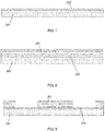
FIG. 6 is a schematic diagram of a cover of the fingerprint identification module according to an embodiment of the present disclosure; -
FIG. 7 is a schematic diagram of a cover and a color coating of the fingerprint identification module according to an embodiment of the present disclosure; -
FIG. 8 is a schematic diagram of a board-level module according to an embodiment of the present disclosure; -
FIG. 9 is a schematic diagram of a hollow area of a board-level module according to an embodiment of the present disclosure; -
FIG. 10 is a schematic diagram of glue filling of the board-level module according to an embodiment of the present disclosure; and -
FIG. 11 is a schematic diagram of attaching of the fingerprint identification chip according to an embodiment of the present disclosure. - Reference numerals and denotations thereof: 100-fingerprint identification chip, 101-identification area, 102-interconnection gold thread, 103-molding layer, 104-substrate layer, 105-pad, 200-fingerprint identification module, 201-filling material, 202-color coating, 203-cover, 204-glue layer, 300-flexible printed circuit, 400-metal ring, and 500-glass cover.
- In order to facilitate understanding of the present disclosure, the present disclosure will be described more comprehensively with reference to relevant drawings. The accompanying drawings show preferential embodiments of the present disclosure. However, the present disclosure may be implemented in a plurality of forms or ways, and is not limited to the embodiments described herein. On the contrary, these embodiments are provided to make the understanding of the disclosed contents of the present disclosure more thorough and comprehensive.
- Unless otherwise defined, all the technical and scientific terms used in this specification are the same as those usually understood by persons skilled in the art of the present disclosure. The terms in the specification of the present disclosure are only used to describe the specific embodiments, but not to limit the present disclosure.
- Referring to
FIG. 1 , afingerprint identification chip 100 included in a fingerprint identification module provided in the embodiments of the present disclosure includes anidentification area 101, aninterconnection gold thread 102, amolding layer 103, asubstrate layer 104 and apad 105. Theidentification area 101 is disposed inside of themolding layer 103, thesubstrate layer 104 is adhered to themolding layer 103, thepad 105 is disposed on an upper surface and a lower surface of thesubstrate layer 104 and is further disposed on an upper surface of theidentification area 101, and thepad 105 on the upper surface of theidentification area 101 is connected to thepad 105 on the upper surface of thesubstrate layer 104 via theinterconnection gold thread 102. - Referring to
FIG. 5 , a fingerprint identification module provided in the embodiments of the present disclosure includes afingerprint identification chip 100, a fillingmaterial 201, acolor coating 202, acover 203 and aglue layer 204. Thecolor coating 202 is disposed between the fillingmaterial 201 and thecover 203, and thefingerprint identification chip 100 is inversely attached in a hollow area of the fillingmaterial 201 in a vacuum environment. The fillingmaterial 201 is a material having a photo-induced effect such as an organic colloid, a film or a plastic. The hollow area is obtained by exposing and developing a part of the fillingmaterial 201. The hollow area is filled with theglue layer 204, which is configured to attach thefingerprint identification chip 100. The fingerprint identification module is manufactured in batches on a board-level module, and is subsequently obtained via dicing. The structure is simple and easy to manufacture. - A method for manufacturing for a fingerprint identification module provided in the embodiments of the present disclosure includes the following steps.
- Step S1: A board-level module is manufactured by using a filling
material 201, acolor coating 202 and acover 203. - Referring to
FIG. 6 , thecover 203 is used as a carrier, and may use such materials as a strip-type glass, a strip-type ceramic, a substrate-type glass, a substrate-type ceramic, or a disc-type glass having the same shape as a wafer. Different sizes may be selected for thecover 203 according to the features of the industry or the wafer level module technology. Referring toFIG. 7 , thecolor coating 202 may be coated on thecover 203 by using such processes as silk screening, and a specific color may be customized according to customer's needs. - Referring to
FIG. 8 , a layer of the fillingmaterial 201 is coated on thecolor coating 202, the fillingmaterial 201 may be a material having a photo-induced effect such as an organic colloid, a film or a plastic, and the thickness of the filling material is customized according to the thickness of thefingerprint identification chip 100. - Step S2: An array of hollow areas in a predetermined quantity is processed on the filling
material 201 of the board-level module. - Referring to
FIG. 9 , with respect to step S2, since the fillingmaterial 201 has the photo-induced effect, the hollow area may be acquired by a photolithography process such as, exposing and developing the fillingmaterial 201. After the fillingmaterial 201 is hollowed, the size of each hollow area is a little bit greater than that of thefingerprint identification chip 100, and the fillingmaterial 201 may surround and support thefingerprint identification chip 100, and thus protect thefingerprint identification chip 100. A plurality of hollow area arrays may be manufactured on the fillingmaterial 201 of the same board-level module for manufacturing of the fingerprint identification module, such that the materials and processes are reduced, and the production efficiency is improved. - Step S3: The
fingerprint identification chip 100 is attached into each hollow area in the array of hollow areas of the filling material in a vacuum environment. - In step S3, the attaching a
fingerprint identification chip 100 into each hollow area in the array of hollow areas of the fillingmaterial 201 includes the following steps. - S31: A glue with a preset thickness is uniformly filled at a bottom of each of the hollow areas, and a defoaming process is performed for the glue.
- Referring to
FIG. 10 , the bottom of each of the hollow areas is coated by theglue layer 204, such that the glue with a suitable thickness is uniformly filled at the bottom of the hollow area. In addition, the defoaming process is performed for theglue layer 204 to eliminate the bubbles. - S32: The
fingerprint identification chip 100 is inversely placed in each hollow area in the array of hollow areas of the fillingmaterial 201. - The manufactured board-level module is placed in a vacuum environment, and the atmospheric environment that exists in the hollow area is cleared. In addition, the
fingerprint identification chip 100 is inversely placed in the hollow area, and an upper surface of the inversely-placedfingerprint identification chip 100 is above an upper surface of the fillingmaterial 201. - S33: The
fingerprint identification chip 100 is pressurized and heated, such that thefingerprint identification chip 100 is tightly attached to the glue and the glue is solidified. - Referring to
FIG. 11 , with respect to step S33, in the vacuum environment, when being attached, thefingerprint identification chip 100 may be suitably pressurized and heated, such that theglue layer 204 is solidified, and the bubbles between thefingerprint identification chip 100 and thecover 203 may be greatly eliminated. - Step S4: The board-level module is diced to obtain fingerprint identification modules.
- Since the size of the
cover 203 may be 8 inches, 12 inches, or bigger, hundreds of hollow areas may be formed at one time on a corresponding board-level module. When the manufacture is performed at a time, a plurality of fingerprint identification modules may be manufactured on the board-level module. After the manufacture, the plurality of fingerprint identification modules on the same board-level module may be diced, such that a plurality of attached fingerprint identification modules may be obtained, which improves the production efficiency, and facilitates large-scale mass production. - The foregoing method for manufacturing the fingerprint identification module is not limited to manufacturing the fingerprint identification module of the present disclosure.
- The embodiments provided in the present disclosure create the follow beneficial effects:
- 1. The
fingerprint identification module 200 according to the embodiments of the present disclosure is obtained by dicing a board-level module, and includes afingerprint identification chip 100, a fillingmaterial 201, acolor coating 202 and acover 203. Thecolor coating 202 is disposed between the fillingmaterial 201 and thecover 203, and thefingerprint identification chip 100 is inversely attached in a hollow area of the fillingmaterial 201 in a vacuum environment. This fingerprint identification module has a simple structure, and is easy to manufacture. - 2. The method for manufacturing the fingerprint identification module according to the embodiments of the present disclosure includes: manufacturing a board-level module using a filling
material 201, acolor coating 202 and acover 203, and processing an array of hollow areas in a predetermined quantity on the fillingmaterial 201 of the board-level module; attaching afingerprint identification chip 100 into each hollow area in the array of hollow areas of the fillingmaterial 201 in a vacuum environment; and dicing the board-level module to obtain a plurality of fingerprint identification modules. The method effectively eliminates bubbles between thefingerprint identification chip 100 and thecover 203, and improves the manufacture efficiency of the fingerprint identification module. - Detailed above are exemplary implementation manners of the present disclosure, but the implementation manners of the present disclosure are not limited by the above embodiments. Any change, modification, replacement, combination, and simplification made within the spirit and principle of present disclosure should be equivalent displacement manners, and shall fall within the protection scope of the present disclosure.
Claims (10)
- A fingerprint identification module, wherein the fingerprint identification module is obtained by dicing a board-level module, comprising: a fingerprint identification chip, a filling material, a color coating and a cover;
wherein the color coating is disposed between the filling material and the cover, and the fingerprint identification chip is inversely attached in a hollow area of the filling material in a vacuum environment. - The fingerprint identification module according to claim 1, wherein the fingerprint identification chip comprises an identification area, an interconnection gold thread, a molding layer, a substrate layer and a pad;
wherein the identification area is disposed inside of the molding layer, the substrate layer is adhered to the molding layer, the pad is disposed on an upper surface and a lower surface of the substrate layer and is further disposed on an upper surface of the identification area, and the pad on the upper surface of the identification area is connected to the pad on the upper surface of the substrate layer via the interconnection gold thread. - The fingerprint identification module according to claim 1, wherein an upper surface of the inversely-attached fingerprint identification chip is above an upper surface of the filling material.
- The fingerprint identification module according to claim 1, wherein the filling material is an organic colloid, a film or a plastic, and has a photo-induced effect; and
the hollow area is obtained by exposing and developing a part of the filling material. - The fingerprint identification module according to any one of claims 1 to 4, wherein the cover is a strip-type glass, a strip-type ceramic, a substrate-type glass, a substrate-type ceramic, or a disc-type glass having the same shape as a wafer.
- A method for manufacturing a fingerprint identification module, wherein the method comprises:manufacturing a board-level module comprising a filling material, a color coating and a cover, and processing an array of hollow areas in a predetermined quantity on the filling material of the board-level module;attaching a fingerprint identification chip into each hollow area in the array of hollow areas of the filling material in a vacuum environment; anddicing the board-level module to obtain fingerprint identification modules.
- The method according to claim 6, wherein the attaching a fingerprint identification chip into each hollow area in the array of hollow areas of the filling material comprises:uniformly filling a glue with a preset thickness at a bottom of each of the hollow areas, and performing a defoaming process to the glue;inversely placing the fingerprint identification chip in each hollow area in the array of hollow areas of the filling material; andpressurizing the fingerprint identification chip and heating to cure the fingerprint identification chip, such that the fingerprint identification chip is tightly attached to the glue and the glue is solidified.
- The method according to claim 7, wherein an upper surface of the inversely-placed fingerprint identification chip is above an upper surface of the filling material.
- The method according to claim 6, wherein the filling material is an organic colloid, a film or a plastic, and has a photo-induced effect; and
each hollow area in the array of hollow areas of the filling material is obtained by exposing and developing the filling material. - The method according to any one of claims 6 to 9, wherein the cover is a strip-type glass, a strip-type ceramic, a substrate-type glass, a substrate-type ceramic, or a disc-type glass having the same shape as a wafer.
Applications Claiming Priority (1)
| Application Number | Priority Date | Filing Date | Title |
|---|---|---|---|
| PCT/CN2016/090101 WO2018010158A1 (en) | 2016-07-15 | 2016-07-15 | Fingerprint recognition module and preparation method therefor |
Publications (2)
| Publication Number | Publication Date |
|---|---|
| EP3288072A1 true EP3288072A1 (en) | 2018-02-28 |
| EP3288072A4 EP3288072A4 (en) | 2018-05-23 |
Family
ID=60941664
Family Applications (1)
| Application Number | Title | Priority Date | Filing Date |
|---|---|---|---|
| EP16889672.8A Withdrawn EP3288072A4 (en) | 2016-07-15 | 2016-07-15 | Fingerprint recognition module and preparation method therefor |
Country Status (5)
| Country | Link |
|---|---|
| US (1) | US10350869B2 (en) |
| EP (1) | EP3288072A4 (en) |
| KR (1) | KR20180022626A (en) |
| CN (1) | CN108140623B (en) |
| WO (1) | WO2018010158A1 (en) |
Families Citing this family (7)
| Publication number | Priority date | Publication date | Assignee | Title |
|---|---|---|---|---|
| CN108205650B (en) * | 2016-12-20 | 2021-11-30 | 致伸科技股份有限公司 | Fingerprint identification module |
| TWI642158B (en) * | 2017-07-21 | 2018-11-21 | Primax Electronics Ltd. | Fingerprint sensing chip package structure |
| TWI627720B (en) * | 2017-08-25 | 2018-06-21 | Primax Electronics Ltd. | Fingerprint sensing chip package structure |
| CN109492480A (en) * | 2017-09-12 | 2019-03-19 | 南昌欧菲生物识别技术有限公司 | Ultrasonic wave biological identification device and electronic equipment |
| CN111968948A (en) * | 2020-08-28 | 2020-11-20 | 江苏凯尔生物识别科技有限公司 | Fingerprint module and production process thereof |
| CN112420533B (en) * | 2020-12-23 | 2025-02-07 | 星科金朋半导体(江阴)有限公司 | A mold structure of a fingerprint product and a chip packaging method thereof |
| TWM612841U (en) * | 2021-02-19 | 2021-06-01 | 安帝司股份有限公司 | Fingerprint identification smart card |
Family Cites Families (13)
| Publication number | Priority date | Publication date | Assignee | Title |
|---|---|---|---|---|
| US5546654A (en) * | 1994-08-29 | 1996-08-20 | General Electric Company | Vacuum fixture and method for fabricating electronic assemblies |
| JP5880300B2 (en) * | 2012-06-14 | 2016-03-08 | 日立化成株式会社 | Adhesive composition and semiconductor device using the same |
| CN203102316U (en) * | 2012-10-12 | 2013-07-31 | 周正三 | Biosensor module, assembly and electronic equipment using same |
| KR20140076712A (en) * | 2012-12-13 | 2014-06-23 | (주)파트론 | Fingerprint sensing module and method thereof |
| CN103198547A (en) * | 2013-03-29 | 2013-07-10 | 杨浩 | Fingerprint recognition controller |
| KR20150009481A (en) * | 2013-07-16 | 2015-01-26 | 주식회사 아이피시티 | Fingerprint sensor module for mobile device and manufacturing methode thereof |
| KR20150020024A (en) * | 2013-08-13 | 2015-02-25 | 주식회사 아이피시티 | Fingerprint sensor module, portable electronic device having the same, and manufacturing method thereof |
| CN104916549B (en) * | 2014-10-31 | 2018-08-14 | 深圳市东方聚成科技有限公司 | A kind of sealed in unit of the fingerprint recognition chip with arc side and encapsulation and cutting method |
| TW201631716A (en) * | 2015-02-16 | 2016-09-01 | 精材科技股份有限公司 | Wafer size grade sensing chip package module and manufacturing method thereof |
| CN104866814B (en) * | 2015-04-17 | 2019-09-13 | 业成科技(成都)有限公司 | Fingerprint recognition device and manufacturing method thereof |
| CN105068685B (en) * | 2015-07-30 | 2018-01-19 | 广东欧珀移动通信有限公司 | Terminal |
| CN105046244A (en) | 2015-08-28 | 2015-11-11 | 南昌欧菲生物识别技术有限公司 | Fingerprint identification module group and preparation method therefor as well as electronic equipment provided with fingerprint identification module group |
| TWM516228U (en) * | 2015-09-25 | 2016-01-21 | 茂丞科技股份有限公司 | Fingerprint sensing package module |
-
2016
- 2016-07-15 WO PCT/CN2016/090101 patent/WO2018010158A1/en not_active Ceased
- 2016-07-15 EP EP16889672.8A patent/EP3288072A4/en not_active Withdrawn
- 2016-07-15 KR KR1020177022915A patent/KR20180022626A/en not_active Ceased
- 2016-07-15 CN CN201680000609.6A patent/CN108140623B/en not_active Expired - Fee Related
-
2017
- 2017-08-11 US US15/674,724 patent/US10350869B2/en active Active
Also Published As
| Publication number | Publication date |
|---|---|
| CN108140623B (en) | 2021-06-25 |
| US10350869B2 (en) | 2019-07-16 |
| CN108140623A (en) | 2018-06-08 |
| US20180015711A1 (en) | 2018-01-18 |
| KR20180022626A (en) | 2018-03-06 |
| WO2018010158A1 (en) | 2018-01-18 |
| EP3288072A4 (en) | 2018-05-23 |
Similar Documents
| Publication | Publication Date | Title |
|---|---|---|
| US10350869B2 (en) | Fingerprint identification module and method for manufacturing the same | |
| TWI575670B (en) | A semiconductor device including a separate thin film layer for interposing and/or spacing semiconductor dies | |
| US9118825B2 (en) | Attachment of wafer level optics | |
| US7517725B2 (en) | System and method for separating and packaging integrated circuits | |
| EP1139435A2 (en) | Chip scale packaging for optical image sensing integrated circuits | |
| US7579215B2 (en) | Method for fabricating a low cost integrated circuit (IC) package | |
| US8293572B2 (en) | Injection molding system and method of chip package | |
| WO2017007425A1 (en) | Optoelectronic modules including overmold supporting an optical assembly | |
| CN101425469A (en) | Semiconductor packaging method using large-size panel | |
| CN105895540A (en) | Die back surface silicone printing encapsulation method | |
| US20100013041A1 (en) | Microelectronic imager packages with covers having non-planar surface features | |
| CN112106207A (en) | Optoelectronic module and wafer-level method for producing an optoelectronic module | |
| US20120098080A1 (en) | Method and package for an electro-optical semiconductor device | |
| CN110731006B (en) | Method and apparatus for chip level packaging | |
| CN101431050B (en) | Manufacture the method for multiple semiconductor devices | |
| CN111261647A (en) | A light-transmitting cover plate, an optical sensor and a manufacturing method thereof | |
| JP2005322869A (en) | Wafer level package manufacturing tool and chip placement method | |
| CN111017864A (en) | MEMS packaging part based on 3D printing and packaging method | |
| JPH10135254A (en) | Semiconductor device manufacturing method and semiconductor device | |
| US7288847B2 (en) | Assembly including a circuit and an encapsulation frame, and method of making the same | |
| KR101589242B1 (en) | A sputtering method for EMI shielding of the semiconductor package | |
| EP3175481B1 (en) | A multi-chip-module semiconductor chip package having dense package wiring | |
| JP2009099850A (en) | Semiconductor module manufacturing method and manufacturing apparatus, and semiconductor module | |
| CN100454505C (en) | Semiconductor device and method for fabricating the same | |
| JP2009152481A (en) | Imaging semiconductor device and manufacturing method of imaging semiconductor device |
Legal Events
| Date | Code | Title | Description |
|---|---|---|---|
| PUAI | Public reference made under article 153(3) epc to a published international application that has entered the european phase |
Free format text: ORIGINAL CODE: 0009012 |
|
| 17P | Request for examination filed |
Effective date: 20170821 |
|
| AK | Designated contracting states |
Kind code of ref document: A1 Designated state(s): AL AT BE BG CH CY CZ DE DK EE ES FI FR GB GR HR HU IE IS IT LI LT LU LV MC MK MT NL NO PL PT RO RS SE SI SK SM TR |
|
| AX | Request for extension of the european patent |
Extension state: BA ME |
|
| RIN1 | Information on inventor provided before grant (corrected) |
Inventor name: WU, BAOQUAN Inventor name: LONG, WEI |
|
| RIN1 | Information on inventor provided before grant (corrected) |
Inventor name: LONG, WEI Inventor name: WU, BAOQUAN |
|
| A4 | Supplementary search report drawn up and despatched |
Effective date: 20180420 |
|
| RIC1 | Information provided on ipc code assigned before grant |
Ipc: H01L 27/146 20060101ALI20180413BHEP Ipc: H01L 21/50 20060101ALI20180413BHEP Ipc: H01L 23/28 20060101ALI20180413BHEP Ipc: H01L 23/00 20060101ALI20180413BHEP Ipc: H01L 23/31 20060101AFI20180413BHEP Ipc: G06K 9/00 20060101ALI20180413BHEP Ipc: B32B 37/00 20060101ALN20180413BHEP |
|
| 17Q | First examination report despatched |
Effective date: 20190116 |
|
| STAA | Information on the status of an ep patent application or granted ep patent |
Free format text: STATUS: THE APPLICATION HAS BEEN WITHDRAWN |
|
| 18W | Application withdrawn |
Effective date: 20190508 |