EP3288068A1 - Semiconductor chip having on-chip noise protection circuit - Google Patents
Semiconductor chip having on-chip noise protection circuit Download PDFInfo
- Publication number
- EP3288068A1 EP3288068A1 EP16782935.7A EP16782935A EP3288068A1 EP 3288068 A1 EP3288068 A1 EP 3288068A1 EP 16782935 A EP16782935 A EP 16782935A EP 3288068 A1 EP3288068 A1 EP 3288068A1
- Authority
- EP
- European Patent Office
- Prior art keywords
- pad
- semiconductor chip
- metal
- protective element
- thin film
- Prior art date
- Legal status (The legal status is an assumption and is not a legal conclusion. Google has not performed a legal analysis and makes no representation as to the accuracy of the status listed.)
- Granted
Links
Images






Classifications
-
- H—ELECTRICITY
- H10—SEMICONDUCTOR DEVICES; ELECTRIC SOLID-STATE DEVICES NOT OTHERWISE PROVIDED FOR
- H10D—INORGANIC ELECTRIC SEMICONDUCTOR DEVICES
- H10D84/00—Integrated devices formed in or on semiconductor substrates that comprise only semiconducting layers, e.g. on Si wafers or on GaAs-on-Si wafers
- H10D84/01—Manufacture or treatment
- H10D84/02—Manufacture or treatment characterised by using material-based technologies
- H10D84/03—Manufacture or treatment characterised by using material-based technologies using Group IV technology, e.g. silicon technology or silicon-carbide [SiC] technology
- H10D84/038—Manufacture or treatment characterised by using material-based technologies using Group IV technology, e.g. silicon technology or silicon-carbide [SiC] technology using silicon technology, e.g. SiGe
-
- H—ELECTRICITY
- H10—SEMICONDUCTOR DEVICES; ELECTRIC SOLID-STATE DEVICES NOT OTHERWISE PROVIDED FOR
- H10D—INORGANIC ELECTRIC SEMICONDUCTOR DEVICES
- H10D89/00—Aspects of integrated devices not covered by groups H10D84/00 - H10D88/00
- H10D89/60—Integrated devices comprising arrangements for electrical or thermal protection, e.g. protection circuits against electrostatic discharge [ESD]
- H10D89/601—Integrated devices comprising arrangements for electrical or thermal protection, e.g. protection circuits against electrostatic discharge [ESD] for devices having insulated gate electrodes, e.g. for IGFETs or IGBTs
- H10D89/911—Integrated devices comprising arrangements for electrical or thermal protection, e.g. protection circuits against electrostatic discharge [ESD] for devices having insulated gate electrodes, e.g. for IGFETs or IGBTs using passive elements as protective elements
-
- H—ELECTRICITY
- H10—SEMICONDUCTOR DEVICES; ELECTRIC SOLID-STATE DEVICES NOT OTHERWISE PROVIDED FOR
- H10W—GENERIC PACKAGES, INTERCONNECTIONS, CONNECTORS OR OTHER CONSTRUCTIONAL DETAILS OF DEVICES COVERED BY CLASS H10
- H10W20/00—Interconnections in chips, wafers or substrates
- H10W20/40—Interconnections external to wafers or substrates, e.g. back-end-of-line [BEOL] metallisations or vias connecting to gate electrodes
- H10W20/482—Interconnections external to wafers or substrates, e.g. back-end-of-line [BEOL] metallisations or vias connecting to gate electrodes for individual devices provided for in groups H10D8/00 - H10D48/00, e.g. for power transistors
- H10W20/484—Interconnections having extended contours, e.g. pads having mesh shape or interconnections comprising connected parallel stripes
-
- H—ELECTRICITY
- H10—SEMICONDUCTOR DEVICES; ELECTRIC SOLID-STATE DEVICES NOT OTHERWISE PROVIDED FOR
- H10W—GENERIC PACKAGES, INTERCONNECTIONS, CONNECTORS OR OTHER CONSTRUCTIONAL DETAILS OF DEVICES COVERED BY CLASS H10
- H10W42/00—Arrangements for protection of devices
- H10W42/60—Arrangements for protection of devices protecting against electrostatic charges or discharges, e.g. Faraday shields
-
- H—ELECTRICITY
- H10—SEMICONDUCTOR DEVICES; ELECTRIC SOLID-STATE DEVICES NOT OTHERWISE PROVIDED FOR
- H10W—GENERIC PACKAGES, INTERCONNECTIONS, CONNECTORS OR OTHER CONSTRUCTIONAL DETAILS OF DEVICES COVERED BY CLASS H10
- H10W72/00—Interconnections or connectors in packages
- H10W72/90—Bond pads, in general
- H10W72/981—Auxiliary members, e.g. spacers
- H10W72/983—Reinforcing structures, e.g. collars
Definitions
- the present invention relates to a semiconductor chip having a function of protecting an internal circuit from noise by using a protective circuit formed on a chip.
- the clamp transistor breaks down or snaps back to a low resistance state, and thus, a current flows from the pad to the ground terminal through the polysilicon resistor and the clamp transistor. At this time, most of the energy of noise is absorbed by the polysilicon resistor, and the voltage applied to the internal circuit is clamped to a certain value or less, so that it is possible to prevent the above-mentioned element destruction and deterioration in characteristics.
- the contact is needed in order to connect the pad and the polysilicon resistor, and there is a problem that the contact is easily broken by noise.
- the contact is configured with a metal material such as tungsten, and one polysilicon resistor is configured with a semiconductor material, so parasitic resistance occurs at the junction between the contact and the polysilicon resistor.
- the contact size may be reduced, and thus, the contact is relatively high in resistance. As a result, the energy of noise concentrates on the contact, and the contact may be burned out.
- the present invention has been made in view of the above circumstances, and an object of the present invention is to provide a semiconductor chip having higher reliability by improving noise tolerance of an on-chip noise protective circuit.
- a semiconductor chip in which a resistance value of a metal interconnection on a path leading from a pad to a protective element is higher than a resistance value of the protective element.
- FIG. 1 illustrates a circuit configuration of the semiconductor chip according to the first embodiment.
- FIG. 2 is a diagram illustrating an example of characteristics of a protective element 102.
- FIG. 3 is a cross-sectional diagram including a pad 100 of the semiconductor chip illustrated in FIG. 1 , a metal protective resistor 101, and the protective element 102.
- the configuration of the semiconductor chip according to the embodiment will be described with reference to FIG. 1 .
- the semiconductor chip 106 according to the embodiment is configured to include a pad 100, a metal protective resistor 101, a protective element 102 (hereinafter, the metal protective resistor 101 and the protective element 102 are collectively referred to as a protective circuit 107), a ground 104, and an internal circuit 105 which includes an MOS transistor.
- the pad 100 is configured with a metal material such as aluminum.
- the metal protective resistor 101 is configured with a metal material such as aluminum.
- the protective element 102 is a diode element of which an anode is connected to the ground 104 and of which a cathode is connected to interconnection 108 extending from the metal protective resistor 101 to the internal circuit 105, and for example, the protective element is obtained by forming an N-type diffusion layer on a P-type substrate.
- a resistance value R m of the metal protective resistor 101 is set to be higher than a resistance value R d of the protective element 102.
- the metal interconnection connecting the protective element 102 and the pad 100 has a high resistance portion having a resistance higher than that of the protective element 102 on an electrical path between the protective element 102 and the pad 100.
- FIG. 2 illustrates a current-voltage characteristic of the diode at the time of reverse biasing.
- the diode is reverse-biased with a voltage near an operating voltage Vcc of the internal circuit, and almost no current flows.
- V BD breakdown voltage
- a current I d flows through the diode due to a physical phenomenon called Zener breakdown or avalanche breakdown.
- E m V N 2 ⁇ R m R m + R d 2
- E d V N 2 ⁇ R d R m + R d 2
- V N the noise voltage applied to the pad 100
- R d is defined by dividing the voltage V d across the diode by I d and is defined as including a resistance component of the diode itself and a resistance component of the contact to the diffusion layer.
- the ratio of the energy consumed by the protective resistor and the diode is equal to the ratio of the respective resistances. Since R m is larger than R d in the embodiment, a half or more of the energy of noise can be absorbed by the resistance, and thus, it is possible to prevent the diode element including the contact from being destructed.
- the pad 100 has a function of any one of a power supply terminal, a signal input terminal, a signal output terminal, and a signal input/output terminal.
- the pad 100 is a power supply terminal, it is preferable to set the resistance value R m of the metal protective resistor 101 so as to satisfy the following mathematical formula.
- V IN is a voltage supplied to the pad at the time of using the semiconductor chip
- V CCMIN is a minimum operating voltage of the internal circuit 105
- I CC is current consumption of the internal circuit 105.
- FIG. 3 is a diagram illustrating an example of a cross-sectional structure from the pad 100 to the protective circuit 107 in FIG. 1 .
- the metal protective resistor 101 is configured with the same metal interconnection layer as the pad 100, and an input end 306 of the metal protective resistor 101 is directly connected to the pad 100.
- an output end 307 of the metal protective resistor 101 is connected to a diffusion layer 302 of the protective element 102 through a via 305, a lower metal interconnection layer 304, and a contact 303 to the diffusion layer. According to such a configuration, a contact vulnerable to noise is not required between the pad 100 and the metal protective resistor 101, so that the noise tolerance of the semiconductor chip 106 is improved.
- a reference of the withstand voltage of the oxide film is generally 10 MV/cm, in other words, 1 V per 1 nm. Namely, as the distance between the protective resistor and a substrate 301 increases, the breakdown voltage of the interlayer insulating film between the protective resistor and the substrate is improved.
- the metal protective resistor 101 and the input terminal 306 of the metal protective resistor 101 to which a high voltage caused by noise is directly applied are located at positions separated from the substrate 301, in comparison with the polysilicon protective resistor formed on a field oxide film described in PTL 1, the withstand voltage of the input end 306 of the metal protective resistor 101 to the substrate is improved.
- the metal protective resistor 101 and the substrate 301 is preferably separated by 500 nm or more. Namely, it is preferable that the thickness of the stacked structure of the insulating film formed over the substrate 301 be 500 nm or more, and a metal interconnection film be formed on this stacked structure.
- the number of the metal interconnection layers is two is illustrated, but the number of the metal interconnection layers is not limited to two. Even in the case of one layer or three or more layers, the same effect can be obtained by the same structure.
- the type of the protective element 102 is not limited to a diode.
- a gate-grounded NMOS (ggNMOS) 1201 having a gate and a source connected to the ground as illustrated in FIG. 12 or a PMOS 2201 having a gate and a source connected to a high potential side as illustrated in FIG. 22 may be used.
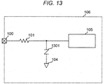
- a varistor element 1301 may be used.
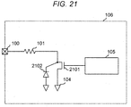
- a parasitic diode 2102 formed between the diffusion layer of the transistor 2101 and the substrate or the well may be used as a protective element.
- the transistor 2101 is not limited to an NMOS transistor illustrated in FIG. 21 , but the transistor may be a PMOS transistor or a bipolar transistor. In the case of a bipolar transistor, the parasitic diode is formed between any one of the collector, the base, and the emitter and the substrate or the well.
- the effects of the semiconductor chip 107 according to the embodiment will be described.
- the first effect is that, since there is no contact vulnerable to noise between the pad 100 and the metal protective resistor 101 and the contact to the protective element 102 is protected by the metal protective resistor 101 of the anterior stage, the protective circuit 107 is hard to be destroyed with respect to noise.
- the second effect is that, since the input terminal of the protective resistor is separated from the substrate in comparison with the polysilicon protective resistor in the related art, the withstand voltage to the substrate is higher, and thus, it is possible to provide a protection function with respect to higher voltage noise.
- FIG. 4 is a top diagram of the protective circuit of the semiconductor chip according to the second embodiment. Description of the same configurations as in the first embodiment will be omitted.
- the protective circuit according to the second embodiment is characterized in that the metal protective resistor 101 in the semiconductor chip 106 according to the first embodiment is configured with a spiral metal interconnection resistor 406.
- the metal interconnection resistor 406 is configured with the same interconnection layer as a pad 400 and is connected to a diffusion layer 403 of the protective element 102 through a via 401, a lower interconnection layer 404, and a contact 402.
- the impedance Z m of the metal protective resistor 101 is expressed by the following mathematical formula.
- Z m R m + j ⁇ L m
- R m is a resistance component of the metal interconnection resistor 101
- ⁇ is an angular frequency of the noise
- L m is inductance of the metal interconnection resistor 101.
- the spiral metal interconnection resistor 406 may be configured to have corner portions. More specifically, the bent angle of the interconnection is allowed to be smaller than 90 degrees.
- FIG. 4 illustrates an example in which corner portions 407 of the metal interconnection resistor 406 are configured by twice bending at 45 degrees.
- the extraction portion from the pad 400 may be formed to have a straight line section 405 to a certain extent. According to such a configuration, it is possible to suppress the damage of the interconnection due to the concentration of the current on the corner portions of the interconnection at the time of applying noise, and thus, it is possible to realize a semiconductor chip having higher reliability.
- FIG. 5 illustrates a modified example of the protective circuit of the semiconductor chip according to the second embodiment.
- the protective circuit according to the embodiment is characterized in that the metal protective resistor 101 is configured with a spiral metal interconnection resistor 501 formed below the pad 100 and the metal protective resistor is arranged below the pad. According to such a configuration, in addition to the same effect as in the second embodiment, since the metal protective resistor 101 is formed between the pad 100 and the contact 303, it is possible to further reduce the area of the protective circuit.
- FIG. 6 is a cross-sectional diagram of a protective circuit of the semiconductor chip according to the third embodiment. Description of the same configurations as in the first embodiment will be omitted.
- the protective circuit 107 according to the third embodiment is characterized in that the metal protective resistor 101 according to the first embodiment is configured with a metal interconnection 601 in the same layer as the pad 100, a metal interconnection 603 below the pad 100, and a via 602 connecting the metal interconnection 601 and the metal interconnection 603.
- the terminal of the metal interconnection 603 closer to the internal circuit is connected to a diffusion layer 606 of the protective element 102 by the contact 605.
- the metal protective resistor 101 is configured by using two metal interconnection layers, but three or more metal interconnection layers may be used. In this case, it is possible to further reduce the area of the metal protective resistor 101.
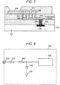
- FIG. 7 illustrates a modified example of the protective circuit of the semiconductor chip according to the third embodiment.
- the metal protective resistor 101 is configured with a plurality of interconnection layers and vias.
- the protective circuit is characterized in that metal interconnection layers 705 and metal interconnection layers 706 below the metal interconnection layers are connected in series through vias 701.
- the high resistance of the protective resistor can be implemented. In other words, in comparison with the same resistance value, it is possible to reduce the area of the resistor.
- the material of the via 701 is a high resistance metal such as tungsten, it is possible to further reduce the area.
- a protective circuit of a semiconductor chip according to a fourth embodiment of the present invention will be described with reference to FIG. 8 .
- the protective circuit according to the embodiment is characterized in that a polysilicon resistor 801 is further connected in series between the protective resistor 101 and the protective element 102 in the semiconductor chip 106 according to the first embodiment.
- FIG. 9 is a diagram illustrating an example of the cross-sectional structure from the pad to the protective circuit in FIG. 8 .
- the protective resistor 101 is configured in the same metal interconnection layer as the pad 100, and the protective resistor 101 is connected to the polysilicon resistor 801 through a via 901 and a contact 902.
- the resistivity of the polysilicon resistor is higher than that of the metal interconnection resistor by one or more ordes of magnitude, and thus, if the same resistance value is used, the polysilicon resistor can be made smaller in area than the metal interconnection resistor.
- the contact 902 to the polysilicon resistor 801 vulnerable to noise is protected by the metal interconnection resistor 101.
- the metal interconnection resistor 101 also has an effect of lowering the voltage applied to the polysilicon resistor 801.
- the noise voltage is lowered by using the metal interconnection resistor 101 having a high withstand voltage to the substrate, the polysilicon resistor having a relatively low withstand voltage to the substrate can also be used.
- a portion of the protective resistor is configured with a polysilicon resistor having high resistivity, so that it is possible to reduce the area when viewed as the whole protective resistor. According to such a configuration, in addition to the same effect as in the first embodiment, it is possible to reduce the area of the resistor in comparison with the first embodiment.
- the metal protective resistor 101 may be configured in the spiral shape described in the second embodiment, in the multiple metal film layer structure described in the third embodiment, or in a combination of the spiral shape in the second embodiment and the multiple metal film layer structure in the third embodiment, and the same effect can be obtained.
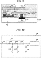
- a protective circuit of a semiconductor chip according to a fifth embodiment of the present invention will be described with reference to FIG. 10 .
- the protective circuit 107 according to the embodiment is characterized in that a protective capacitor 1005 is added in parallel to the metal protective resistor 101 in the first embodiment.
- the metal protective resistor 101 is virtually divided into three series resistors 1002, 1003, and 1004, and protective capacitors 1005 and 1006 are connected between the resistors.
- the number of division and the connection positions of the protective capacitors are not limited thereto.
- the metal protective resistor 101 and the protective capacitors 1005 and 1006 constitute an RC low-pass filter, the peak voltage in the protective circuit according to the embodiment can be lower with respect to high-frequency noise than the protective circuit according to the first embodiment. Therefore, when noise is applied, the voltage applied to the internal circuit is reduced, and thus, it is possible to realize a semiconductor chip having higher reliability.
- FIG. 11 is a top diagram illustrating an example of a structure from the pad to the protective circuit in FIG. 10 .
- the protective circuit is characterized in that electrodes 1101 and 1102 are arranged on both sides of the metal interconnection resistor 101 by using the same metal interconnection layer.
- parasitic capacitance formed between the metal interconnection resistor 101 and the electrode 1101 and parasitic capacitance formed between the metal interconnection resistor 101 and the electrode 1102 are used as protective capacitors 1005 and 1006, respectively.
- an RC low-pass filter can be configured without preparing a special capacitor element, and thus, it is possible to further reduce the area of the protective circuit.
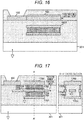
- FIG. 17 illustrates another method of realizing the protective capacitor, and by arranging interconnections 1702, 1703, and 1704 and vias 1705 and 1706 connecting the interconnections so as to stereoscopically surround the upper, lower, left and right sides of the metal interconnection resistor 101, capacitors may be configured between the metal interconnection resistor 101 and the interconnection.
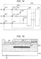
- a sensor device 1400 including a semiconductor chip 1409 according to a sixth embodiment of the present invention will be described with reference to FIG. 14 .
- the sensor device 1400 according to the embodiment is configured to include a sensor element 1413, a semiconductor chip 1409, a power supply terminal 1401, an output terminal 1402, and a ground terminal 1403.
- the sensor element 1413 is an element of which electric characteristic changes according to physical quantities.
- the sensor element 1413 is illustrated as a discrete component, but the sensor element may be formed in the semiconductor chip 1409.
- the semiconductor chip 1409 is configured to include a power supply pad 1410, an output pad 1411, a ground pad 1412, a metal protective resistor 1404, a metal protective resistor 1405, a protective element 1406, a protective element 1407, and an internal circuit 1408.
- the semiconductor chip 1409 controls the sensor element 1413, processes the output signal of the sensor element 1413, and outputs the output signal to the output pad 1411.
- the metal protective resistor 1404 and the metal protective resistor 1405, the protective element 1406 and the protective element 1407 are those illustrated in the above embodiments.
- the power supply terminal 1401 is protected by the protective resistor 1404 and the protective element 1406, and the output terminal 1402 is protected by the protective resistor 1405 and the protective element 1407.
- the semiconductor chip 1409 by providing the semiconductor chip 1409 with tolerance to noise, it is possible to reduce external protective elements of the semiconductor chip 1409, to reduce discrete components included in the sensor device 1400, and to enhance reliability of the sensor device 1400.
- FIG. 15 is a diagram illustrating an example of a cross-sectional structure of a protective circuit of the semiconductor chip according the seventh embodiment.
- the protective circuit 107 according to the embodiment is characterized in that a thin film 1501 having a thermal resistance lower than that of an interlayer insulating film 1502 is arranged between the metal protective resistor 101 and the substrate 301 in the semiconductor chip 106 according to the first embodiment. According to such a configuration, the heat generated by the protective resistor 101 at the time of applying the noise is more easily released to the substrate, and thus, it is possible to enhance the tolerance of the metal protective resistor 101 to the noise energy.
- the interlayer insulating film 1502 is SiO2 (example of thermal resistance value: 0.77 °C ⁇ m/W), and as a material having a thermal resistance lower than that of SiO2, a silicon nitride film Si3N4 (example of thermal resistance value: 0.034 °C ⁇ m/W) or a mixture SiON thereof, aluminum oxide Al203, aluminum nitride AlN, and the like are suitable.
- the thin film 1501 having a thermal resistance lower than that of the interlayer insulating film 1502 is not limited to an insulating film such as a silicon nitride film. As illustrated in FIG.
- a structure 1601 where a metal interconnection layer below the metal protective resistor 101 or a plurality of metal interconnection layers are connected through vias may be used.
- the thermal resistance of the metal material is lower by about one order of magnitude than that of the silicon nitride film, and thus, it is possible to further improve the heat releasing property. As a result, it is possible to increase the tolerance of the protective resistor to the noise energy and to realize a semiconductor chip having higher reliability.
- the embodiment can be applied not only to the first embodiment but also to the other embodiments described above.
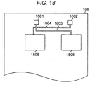
- FIG. 18 is a layout diagram of a plurality of pads 1801 and 1802, metal interconnection resistors 1803 and 1804, and protective elements 1805 and 1806 on the semiconductor chip 106 according to the eighth embodiment.
- the protective circuit 107 according to the embodiment is characterized in that the pads 1801 and 1802 and the protective elements 1805 and 1806 corresponding to the pads 1801 and 1802 are arranged on the semiconductor chip 106 in a cross-cuppled manner and are connected to each other by the metal interconnection resistors 1803 and 1804.
- the metal interconnection resistor can be arranged without expanding the distance between the pads 1801 and 1802 and the protective elements 1805 and, 1806.
- the distance between the pads 1801 and 1802 and the protective element protective elements 1805 and 1806 can be taken without expanding the distance in the vertical direction, it is possible to secure the resistance value of the metal interconnection resistors 1803 and 1804 by suppressing an increase in chip area.
- FIG. 19 is a layout diagram of a plurality of pads 1901 and 1902, metal interconnection resistors 1903 and 1904, and protective elements 1905 and 1906 on the semiconductor chip 106 according to the ninth embodiment.
- the protective circuit according to the embodiment is characterized in that a plurality of the pads 1901 and 1902 and the protective elements 1905 and 1906 corresponding to the pads 1901 and 1902 are arranged on the semiconductor chip 106 along another side of the semiconductor chip 106, and a portion of the metal interconnection resistors 1904 is arranged along a marginal area on the outer periphery of the semiconductor chip 106.
- FIG. 20 is a modified example of the ninth embodiment, and the protective circuit is characterized in that a metal resistor interconnection 2005 connecting a pad 2001 and a protective element 2002 is arranged under a power supply ring 2004 surrounding an internal circuit region 2003. According to such a configuration, since it is unnecessary to secure a new region in order to arrange the metal interconnection resistor, it is possible to secure the resistance value of the metal interconnection resistor by suppressing an increase in chip area.
Landscapes
- Semiconductor Integrated Circuits (AREA)
Abstract
Description
- The present invention relates to a semiconductor chip having a function of protecting an internal circuit from noise by using a protective circuit formed on a chip.
- When an excessive voltage is applied to an internal circuit of a semiconductor chip due to noise such as static electricity or surge, dielectric breakdown of a gate oxide film and destruction or deterioration of PN junction are caused, so that permanent failure, change in circuit characteristics, or the like of the semiconductor chip occur. In order to prevent the destruction or deterioration of the internal circuit caused by such noise and to realize a semiconductor chip having higher reliability, a protective circuit needs to be provided between a pad and the internal circuit so that an excessive voltage is not applied to the internal circuit even when noise is applied. In the technique described in PTL 1, a polysilicon resistor and a clamp transistor are provided between an input pad and an internal circuit. When an excessive voltage is applied to the pad, the clamp transistor breaks down or snaps back to a low resistance state, and thus, a current flows from the pad to the ground terminal through the polysilicon resistor and the clamp transistor. At this time, most of the energy of noise is absorbed by the polysilicon resistor, and the voltage applied to the internal circuit is clamped to a certain value or less, so that it is possible to prevent the above-mentioned element destruction and deterioration in characteristics.
- PTL 1: Japanese Patent Application Publication No.
61-32563 - However, in the technology in the related art, a contact is needed in order to connect the pad and the polysilicon resistor, and there is a problem that the contact is easily broken by noise. In general, the contact is configured with a metal material such as tungsten, and one polysilicon resistor is configured with a semiconductor material, so parasitic resistance occurs at the junction between the contact and the polysilicon resistor. In addition, in recent years, due to miniaturization, the contact size may be reduced, and thus, the contact is relatively high in resistance. As a result, the energy of noise concentrates on the contact, and the contact may be burned out.
- The present invention has been made in view of the above circumstances, and an object of the present invention is to provide a semiconductor chip having higher reliability by improving noise tolerance of an on-chip noise protective circuit.
- According to the present invention for achieving the above object, there is provided a semiconductor chip in which a resistance value of a metal interconnection on a path leading from a pad to a protective element is higher than a resistance value of the protective element.
- According to the present invention, no contact is required between a pad and a protective resistor, and thus, it is possible to provide a semiconductor chip having higher reliability.
-
- [
FIG. 1] FIG. 1 is a diagram illustrating a circuit configuration of a semiconductor chip according to a first embodiment. - [
FIG. 2] FIG. 2 is a diagram illustrating a resistance value of a protective element. - [
FIG. 3] FIG. 3 is a cross-sectional diagram of a semiconductor chip according to the first embodiment. - [
FIG. 4] FIG. 4 is a top diagram of a semiconductor chip according to a second embodiment. - [
FIG. 5] FIG. 5 is a diagram illustrating a modified example of the second embodiment. - [
FIG. 6] FIG. 6 is a cross-sectional diagram of a semiconductor chip according to a third embodiment. - [
FIG. 7] FIG. 7 is a diagram illustrating a modified example of the third embodiment. - [
FIG. 8] FIG. 8 is a diagram illustrating a circuit configuration of a semiconductor chip according to a fourth embodiment. - [
FIG. 9] FIG. 9 is a cross-sectional diagram of a semiconductor chip according to the fourth embodiment. - [
FIG. 10] FIG. 10 is a diagram illustrating a circuit configuration of a semiconductor chip according to a fifth embodiment. - [
FIG. 11] FIG. 11 is a top diagram of a semiconductor chip according to the fifth embodiment. - [
FIG. 12] FIG. 12 is a diagram illustrating a modified example of the first embodiment. - [
FIG. 13] FIG. 13 is a diagram illustrating a modified example of the first embodiment. - [
FIG. 14] FIG. 14 is a diagram illustrating a circuit configuration of a semiconductor chip according to a sixth embodiment. - [
FIG. 15] FIG. 15 is a cross-sectional diagram of a semiconductor chip according to a seventh embodiment. - [
FIG. 16] FIG. 16 is a diagram illustrating a modified example of the seventh embodiment. - [
FIG. 17] FIG. 17 is a diagram illustrating a modified example of the fifth embodiment. - [
FIG. 18] FIG. 18 is a top diagram of a semiconductor chip according to an eighth embodiment. - [
FIG. 19] FIG. 19 is a top diagram of a semiconductor chip according to a ninth embodiment. - [
FIG. 20] FIG. 20 is a diagram illustrating a modified example of the ninth embodiment. - [
FIG. 21] FIG. 21 is a diagram illustrating a modified example of the first embodiment. - [
FIG. 22] FIG. 22 is a diagram illustrating a modified example of the first embodiment. - Hereinafter, embodiments of the present invention will be described with reference to the drawings. A semiconductor chip according to a first embodiment of the present invention will be described with reference to
FIGS. 1 ,2 , and3 .FIG. 1 illustrates a circuit configuration of the semiconductor chip according to the first embodiment.FIG. 2 is a diagram illustrating an example of characteristics of aprotective element 102.FIG. 3 is a cross-sectional diagram including apad 100 of the semiconductor chip illustrated inFIG. 1 , a metalprotective resistor 101, and theprotective element 102. - The configuration of the semiconductor chip according to the embodiment will be described with reference to
FIG. 1 . Thesemiconductor chip 106 according to the embodiment is configured to include apad 100, a metalprotective resistor 101, a protective element 102 (hereinafter, the metalprotective resistor 101 and theprotective element 102 are collectively referred to as a protective circuit 107), aground 104, and aninternal circuit 105 which includes an MOS transistor. Thepad 100 is configured with a metal material such as aluminum. Like thepad 100, the metalprotective resistor 101 is configured with a metal material such as aluminum. Theprotective element 102 is a diode element of which an anode is connected to theground 104 and of which a cathode is connected tointerconnection 108 extending from the metalprotective resistor 101 to theinternal circuit 105, and for example, the protective element is obtained by forming an N-type diffusion layer on a P-type substrate. A resistance value Rm of the metalprotective resistor 101 is set to be higher than a resistance value Rd of theprotective element 102. In other words, the metal interconnection connecting theprotective element 102 and thepad 100 has a high resistance portion having a resistance higher than that of theprotective element 102 on an electrical path between theprotective element 102 and thepad 100. - Operations at the time of applying noise in the embodiment will be described with reference to
FIG. 2. FIG. 2 illustrates a current-voltage characteristic of the diode at the time of reverse biasing. During a normal operation of thesemiconductor chip 106, the diode is reverse-biased with a voltage near an operating voltage Vcc of the internal circuit, and almost no current flows. On the other hand, when noise is applied to thepad 100 and a voltage across the diode becomes equal to or higher than a breakdown voltage VBD, a current Id flows through the diode due to a physical phenomenon called Zener breakdown or avalanche breakdown. At this time, if the energy consumed by the metalprotective resistor 101 and the energy consumed by the diode are denoted by Em and Ed, respectively, the following relationship is satisfied.
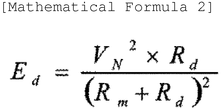
pad 100 is denoted by VN. In addition, Rd is defined by dividing the voltage Vd across the diode by Id and is defined as including a resistance component of the diode itself and a resistance component of the contact to the diffusion layer. In addition, since the current consumption of theinternal circuit 105 is very small in comparison with the current Id at the time of breakdown of the diode, the current consumption is neglected herein. As can be seen from Mathematical Formulas 1 and 2, the ratio of the energy consumed by the protective resistor and the diode is equal to the ratio of the respective resistances. Since Rm is larger than Rd in the embodiment, a half or more of the energy of noise can be absorbed by the resistance, and thus, it is possible to prevent the diode element including the contact from being destructed. - In the
semiconductor chip 106, thepad 100 has a function of any one of a power supply terminal, a signal input terminal, a signal output terminal, and a signal input/output terminal. In the case where thepad 100 is a power supply terminal, it is preferable to set the resistance value Rm of the metalprotective resistor 101 so as to satisfy the following mathematical formula.
- Herein, VIN is a voltage supplied to the pad at the time of using the semiconductor chip, VCCMIN is a minimum operating voltage of the
internal circuit 105, and ICC is current consumption of theinternal circuit 105. By setting Rm to be within the range of the mathematical formula (Mathematical Formula 3), it is possible to prevent theinternal circuit 105 from malfunctioning due to the voltage drop caused by the protective resistor during a normal operation, and thus, it is possible to realize a semiconductor chip having higher reliability. -
FIG. 3 is a diagram illustrating an example of a cross-sectional structure from thepad 100 to theprotective circuit 107 inFIG. 1 . The metalprotective resistor 101 is configured with the same metal interconnection layer as thepad 100, and aninput end 306 of the metalprotective resistor 101 is directly connected to thepad 100. On the other hand, anoutput end 307 of the metalprotective resistor 101 is connected to adiffusion layer 302 of theprotective element 102 through a via 305, a lower metal interconnection layer 304, and acontact 303 to the diffusion layer. According to such a configuration, a contact vulnerable to noise is not required between thepad 100 and the metalprotective resistor 101, so that the noise tolerance of thesemiconductor chip 106 is improved. Another advantage of this configuration is an improvement in the withstand voltage of the protective resistor to the substrate. A reference of the withstand voltage of the oxide film is generally 10 MV/cm, in other words, 1 V per 1 nm. Namely, as the distance between the protective resistor and asubstrate 301 increases, the breakdown voltage of the interlayer insulating film between the protective resistor and the substrate is improved. In this configuration, since the metalprotective resistor 101 and theinput terminal 306 of the metalprotective resistor 101 to which a high voltage caused by noise is directly applied are located at positions separated from thesubstrate 301, in comparison with the polysilicon protective resistor formed on a field oxide film described in PTL 1, the withstand voltage of theinput end 306 of the metalprotective resistor 101 to the substrate is improved. In the electrostatic test, depending on the standard, a voltage of 200 to 500 V is instantaneously applied to the pad, so in order to prevent dielectric breakdown of the interlayer insulating film between the metalprotective resistor 101 and thesubstrate 301, the metalprotective resistor 101 and thesubstrate 301 is preferably separated by 500 nm or more. Namely, it is preferable that the thickness of the stacked structure of the insulating film formed over thesubstrate 301 be 500 nm or more, and a metal interconnection film be formed on this stacked structure. In the example illustrated inFIG. 3 , the case where the number of the metal interconnection layers is two is illustrated, but the number of the metal interconnection layers is not limited to two. Even in the case of one layer or three or more layers, the same effect can be obtained by the same structure. - In addition, the type of the
protective element 102 is not limited to a diode. For example, a gate-grounded NMOS (ggNMOS) 1201 having a gate and a source connected to the ground as illustrated inFIG. 12 or aPMOS 2201 having a gate and a source connected to a high potential side as illustrated inFIG. 22 may be used. In addition, as illustrated inFIG. 13 , avaristor element 1301 may be used. In addition, as illustrated inFIG. 21 , in the case where a drain diffusion layer of thetransistor 2101 is connected to the metalprotective resistor 101, aparasitic diode 2102 formed between the diffusion layer of thetransistor 2101 and the substrate or the well may be used as a protective element. Thetransistor 2101 is not limited to an NMOS transistor illustrated inFIG. 21 , but the transistor may be a PMOS transistor or a bipolar transistor. In the case of a bipolar transistor, the parasitic diode is formed between any one of the collector, the base, and the emitter and the substrate or the well. - The effects of the
semiconductor chip 107 according to the embodiment will be described. The first effect is that, since there is no contact vulnerable to noise between thepad 100 and the metalprotective resistor 101 and the contact to theprotective element 102 is protected by the metalprotective resistor 101 of the anterior stage, theprotective circuit 107 is hard to be destroyed with respect to noise. The second effect is that, since the input terminal of the protective resistor is separated from the substrate in comparison with the polysilicon protective resistor in the related art, the withstand voltage to the substrate is higher, and thus, it is possible to provide a protection function with respect to higher voltage noise. - A protective circuit of a semiconductor chip according to a second embodiment of the present invention will be described with reference to
FIG. 4. FIG. 4 is a top diagram of the protective circuit of the semiconductor chip according to the second embodiment. Description of the same configurations as in the first embodiment will be omitted. The protective circuit according to the second embodiment is characterized in that the metalprotective resistor 101 in thesemiconductor chip 106 according to the first embodiment is configured with a spiralmetal interconnection resistor 406. Themetal interconnection resistor 406 is configured with the same interconnection layer as apad 400 and is connected to adiffusion layer 403 of theprotective element 102 through a via 401, alower interconnection layer 404, and acontact 402. According to such a configuration, in addition to the same effect as in thesemiconductor chip 106 illustrated in the first embodiment, due to an inductance component of the spiral metal interconnection, higher impedance to noise having a high frequency component such as static electricity can be provided to the metalprotective resistor 101. Specifically, the impedance Zm of the metalprotective resistor 101 is expressed by the following mathematical formula.
- Herein, Rm is a resistance component of the
metal interconnection resistor 101, ω is an angular frequency of the noise, and Lm is inductance of themetal interconnection resistor 101. Assuming that the noise voltage is VN and the ON resistance of the protective element is Rd, the voltage Vd applied to the internal circuit can be obtained by the following mathematical formula.
- As can be seen from Mathematical Formula 5, the voltage applied to the internal circuit at the time of applying the noise is lowered by the inductance of the
metal interconnection resistor 101. In other words, the protection performance of the metalprotective resistor 101 improves. - More preferably, the spiral
metal interconnection resistor 406 may be configured to have corner portions. More specifically, the bent angle of the interconnection is allowed to be smaller than 90 degrees.FIG. 4 illustrates an example in whichcorner portions 407 of themetal interconnection resistor 406 are configured by twice bending at 45 degrees. In addition, the extraction portion from thepad 400 may be formed to have astraight line section 405 to a certain extent. According to such a configuration, it is possible to suppress the damage of the interconnection due to the concentration of the current on the corner portions of the interconnection at the time of applying noise, and thus, it is possible to realize a semiconductor chip having higher reliability. -
FIG. 5 illustrates a modified example of the protective circuit of the semiconductor chip according to the second embodiment. The protective circuit according to the embodiment is characterized in that the metalprotective resistor 101 is configured with a spiralmetal interconnection resistor 501 formed below thepad 100 and the metal protective resistor is arranged below the pad. According to such a configuration, in addition to the same effect as in the second embodiment, since the metalprotective resistor 101 is formed between thepad 100 and thecontact 303, it is possible to further reduce the area of the protective circuit. - A protective circuit of a semiconductor chip according to a third embodiment of the present invention will be described with reference to
FIG. 6. FIG. 6 is a cross-sectional diagram of a protective circuit of the semiconductor chip according to the third embodiment. Description of the same configurations as in the first embodiment will be omitted. Theprotective circuit 107 according to the third embodiment is characterized in that the metalprotective resistor 101 according to the first embodiment is configured with ametal interconnection 601 in the same layer as thepad 100, ametal interconnection 603 below thepad 100, and a via 602 connecting themetal interconnection 601 and themetal interconnection 603. The terminal of themetal interconnection 603 closer to the internal circuit is connected to adiffusion layer 606 of theprotective element 102 by thecontact 605. According to such a configuration, in addition to the same effect as in the first embodiment, it is possible to secure a larger interconnection length with the same resistance area as in the first embodiment. Namely, the high resistance of the protective resistor can be implemented. In other words, in comparison with the same resistance value, it is possible to reduce the area of the resistor. InFIG. 6 , the metalprotective resistor 101 is configured by using two metal interconnection layers, but three or more metal interconnection layers may be used. In this case, it is possible to further reduce the area of the metalprotective resistor 101. -
FIG. 7 illustrates a modified example of the protective circuit of the semiconductor chip according to the third embodiment. In the protective circuit according to the modified example, the metalprotective resistor 101 is configured with a plurality of interconnection layers and vias. Namely, the protective circuit is characterized in that metal interconnection layers 705 and metal interconnection layers 706 below the metal interconnection layers are connected in series throughvias 701. According to such a configuration, in addition to the same effect as in the first embodiment, it is possible to secure a larger interconnection length with the same resistance area as in the first embodiment. Namely, the high resistance of the protective resistor can be implemented. In other words, in comparison with the same resistance value, it is possible to reduce the area of the resistor. In addition, if the material of thevia 701 is a high resistance metal such as tungsten, it is possible to further reduce the area. - A protective circuit of a semiconductor chip according to a fourth embodiment of the present invention will be described with reference to
FIG. 8 . The protective circuit according to the embodiment is characterized in that apolysilicon resistor 801 is further connected in series between theprotective resistor 101 and theprotective element 102 in thesemiconductor chip 106 according to the first embodiment. -
FIG. 9 is a diagram illustrating an example of the cross-sectional structure from the pad to the protective circuit inFIG. 8 . Theprotective resistor 101 is configured in the same metal interconnection layer as thepad 100, and theprotective resistor 101 is connected to thepolysilicon resistor 801 through a via 901 and acontact 902. In general, the resistivity of the polysilicon resistor is higher than that of the metal interconnection resistor by one or more ordes of magnitude, and thus, if the same resistance value is used, the polysilicon resistor can be made smaller in area than the metal interconnection resistor. In the embodiment, thecontact 902 to thepolysilicon resistor 801 vulnerable to noise is protected by themetal interconnection resistor 101. In addition, themetal interconnection resistor 101 also has an effect of lowering the voltage applied to thepolysilicon resistor 801. The noise voltage is lowered by using themetal interconnection resistor 101 having a high withstand voltage to the substrate, the polysilicon resistor having a relatively low withstand voltage to the substrate can also be used. On the other hand, a portion of the protective resistor is configured with a polysilicon resistor having high resistivity, so that it is possible to reduce the area when viewed as the whole protective resistor. According to such a configuration, in addition to the same effect as in the first embodiment, it is possible to reduce the area of the resistor in comparison with the first embodiment. As a modified example of the fourth embodiment, the metalprotective resistor 101 may be configured in the spiral shape described in the second embodiment, in the multiple metal film layer structure described in the third embodiment, or in a combination of the spiral shape in the second embodiment and the multiple metal film layer structure in the third embodiment, and the same effect can be obtained. - A protective circuit of a semiconductor chip according to a fifth embodiment of the present invention will be described with reference to
FIG. 10 . Theprotective circuit 107 according to the embodiment is characterized in that aprotective capacitor 1005 is added in parallel to the metalprotective resistor 101 in the first embodiment. InFIG. 10 , for the convenience of description, the metalprotective resistor 101 is virtually divided into threeseries resistors protective capacitors protective resistor 101 and theprotective capacitors -
FIG. 11 is a top diagram illustrating an example of a structure from the pad to the protective circuit inFIG. 10 . The protective circuit is characterized in thatelectrodes metal interconnection resistor 101 by using the same metal interconnection layer. By fixing theelectrodes metal interconnection resistor 101 and theelectrode 1101 and parasitic capacitance formed between themetal interconnection resistor 101 and theelectrode 1102 are used asprotective capacitors - The method of realizing the
protective capacitors FIG. 10 . For example,FIG. 17 illustrates another method of realizing the protective capacitor, and by arranginginterconnections metal interconnection resistor 101, capacitors may be configured between themetal interconnection resistor 101 and the interconnection. - A
sensor device 1400 including asemiconductor chip 1409 according to a sixth embodiment of the present invention will be described with reference toFIG. 14 . Thesensor device 1400 according to the embodiment is configured to include asensor element 1413, asemiconductor chip 1409, apower supply terminal 1401, anoutput terminal 1402, and aground terminal 1403. Thesensor element 1413 is an element of which electric characteristic changes according to physical quantities. InFIG. 14 , thesensor element 1413 is illustrated as a discrete component, but the sensor element may be formed in thesemiconductor chip 1409. Thesemiconductor chip 1409 is configured to include apower supply pad 1410, anoutput pad 1411, aground pad 1412, a metalprotective resistor 1404, a metalprotective resistor 1405, aprotective element 1406, aprotective element 1407, and aninternal circuit 1408. Thesemiconductor chip 1409 controls thesensor element 1413, processes the output signal of thesensor element 1413, and outputs the output signal to theoutput pad 1411. The metalprotective resistor 1404 and the metalprotective resistor 1405, theprotective element 1406 and theprotective element 1407 are those illustrated in the above embodiments. From noise such as static electricity or surge applied from the outside of thesensor device 1400 to theterminals power supply terminal 1401 is protected by theprotective resistor 1404 and theprotective element 1406, and theoutput terminal 1402 is protected by theprotective resistor 1405 and theprotective element 1407. According to such a configuration, by providing thesemiconductor chip 1409 with tolerance to noise, it is possible to reduce external protective elements of thesemiconductor chip 1409, to reduce discrete components included in thesensor device 1400, and to enhance reliability of thesensor device 1400. - A protective circuit of a semiconductor chip according to a seventh embodiment of the present invention will be described with reference to
FIG. 15. FIG. 15 is a diagram illustrating an example of a cross-sectional structure of a protective circuit of the semiconductor chip according the seventh embodiment. Theprotective circuit 107 according to the embodiment is characterized in that athin film 1501 having a thermal resistance lower than that of aninterlayer insulating film 1502 is arranged between the metalprotective resistor 101 and thesubstrate 301 in thesemiconductor chip 106 according to the first embodiment. According to such a configuration, the heat generated by theprotective resistor 101 at the time of applying the noise is more easily released to the substrate, and thus, it is possible to enhance the tolerance of the metalprotective resistor 101 to the noise energy. As a result, it is possible to realize a more reliable semiconductor chip. For example, theinterlayer insulating film 1502 is SiO2 (example of thermal resistance value: 0.77 °C·m/W), and as a material having a thermal resistance lower than that of SiO2, a silicon nitride film Si3N4 (example of thermal resistance value: 0.034 °C·m/W) or a mixture SiON thereof, aluminum oxide Al203, aluminum nitride AlN, and the like are suitable. In addition, thethin film 1501 having a thermal resistance lower than that of theinterlayer insulating film 1502 is not limited to an insulating film such as a silicon nitride film. As illustrated inFIG. 16 , astructure 1601 where a metal interconnection layer below the metalprotective resistor 101 or a plurality of metal interconnection layers are connected through vias may be used. In general, the thermal resistance of the metal material is lower by about one order of magnitude than that of the silicon nitride film, and thus, it is possible to further improve the heat releasing property. As a result, it is possible to increase the tolerance of the protective resistor to the noise energy and to realize a semiconductor chip having higher reliability. The embodiment can be applied not only to the first embodiment but also to the other embodiments described above. - A protective circuit of a semiconductor chip according to an eighth embodiment of the present invention will be described with reference to
FIG. 18. FIG. 18 is a layout diagram of a plurality ofpads metal interconnection resistors protective elements semiconductor chip 106 according to the eighth embodiment. Theprotective circuit 107 according to the embodiment is characterized in that thepads protective elements pads semiconductor chip 106 in a cross-cuppled manner and are connected to each other by themetal interconnection resistors pads protective elements FIG. 18 , since the distance between thepads protective elements metal interconnection resistors - A protective circuit of a semiconductor chip according to a ninth embodiment of the present invention will be described with reference to
FIG. 19. FIG. 19 is a layout diagram of a plurality ofpads metal interconnection resistors protective elements semiconductor chip 106 according to the ninth embodiment. The protective circuit according to the embodiment is characterized in that a plurality of thepads protective elements pads semiconductor chip 106 along another side of thesemiconductor chip 106, and a portion of themetal interconnection resistors 1904 is arranged along a marginal area on the outer periphery of thesemiconductor chip 106. According to such a configuration, since themetal interconnection resistor 1904 can be arranged by utilizing the marginal area on the outer periphery of thesemiconductor chip 106, the resistance value of themetal interconnection resistor 1904 can be secured by suppressing an increase in chip area.FIG. 20 is a modified example of the ninth embodiment, and the protective circuit is characterized in that ametal resistor interconnection 2005 connecting apad 2001 and aprotective element 2002 is arranged under apower supply ring 2004 surrounding aninternal circuit region 2003. According to such a configuration, since it is unnecessary to secure a new region in order to arrange the metal interconnection resistor, it is possible to secure the resistance value of the metal interconnection resistor by suppressing an increase in chip area. -
- 100
- pad
- 101
- metal protective resistor
- 102
- protective element
- 104
- ground terminal
- 105
- internal circuit
- 106
- semiconductor chip
- 107
- protective circuit
- 108
- interconnection
- 301
- substrate
- 302
- diffusion layer
- 303
- contact
- 304
- metal interconnection layer
- 305
- via
- 306
- input end
- 307
- output end
- 401
- via
- 402
- contact
- 403
- diffusion layer
- 404
- interconnection layer
- 405
- straight line section
- 406
- metal interconnection resistor
- 407
- corner portion
- 501
- metal interconnection resistor
- 502
- via
- 503
- contact
- 504
- diffusion layer
- 601
- metal interconnection
- 602
- via
- 603
- metal interconnection
- 604
- interconnection
- 605
- contact
- 606
- diffusion layer
- 701
- via
- 702
- interconnection
- 703
- contact
- 704
- diffusion layer
- 705
- metal interconnection layer
- 706
- metal interconnection layer
- 801
- polysilicon resistor
- 901
- via
- 902
- contact
- 903
- contact
- 904
- interconnection
- 905
- contact
- 906
- diffusion layer
- 1002
- metal interconnection resistor
- 1003
- metal interconnection resistor
- 1004
- metal interconnection resistor
- 1005
- protective capacitor
- 1006
- protective capacitor
- 1101
- electrode
- 1102
- electrode
- 1103
- diffusion layer
- 1104
- interconnection
- 1105
- via
- 1106
- contact
- 1201
- ggNMOS
- 1301
- varistor
- 1400
- sensor device
- 1401
- power supply terminal
- 1402
- output terminal
- 1403
- ground terminal
- 1404
- metal protective resistor
- 1405
- metal protective resistor
- 1406
- protective element
- 1407
- protective element
- 1408
- internal circuit
- 1409
- semiconductor chip
- 1410
- power supply pad
- 1411
- output pad
- 1412
- ground pad
- 1501
- thin film
- 1502
- interlayer insulating film
- 1601
- a structure in which a plurality of metal interconnection layers are connected by vias
- 1702
- metal interconnection layer
- 1703
- metal interconnection layer
- 1704
- metal interconnection layer
- 1705
- via
- 1706
- via
- 1801
- pad
- 1802
- pad
- 1803
- metal interconnection resistor
- 1804
- metal interconnection resistor
- 1805
- protective element
- 1806
- protective element
- 1901
- pad
- 1902
- pad
- 1903
- metal interconnection resistor
- 1904
- metal interconnection resistor
- 1905
- protective element
- 1906
- protective element
- 2001
- pad
- 2002
- protective element
- 2003
- internal circuit region
- 2004
- power supply ring
- 2005
- metal interconnection resistor
- 2101
- transistor
- 2102
- parasitic diode
- 2201
- PMOS
- Rm
- resistance value
- Id
- current
- Vd
- voltage
- Rd
- resistance value
- VN
- noise voltage
- VCC
- power supply
- Out
- output
- Gnd
- ground
- VBD
- breakdown voltage
Claims (14)
- A semiconductor chip comprising:a pad;a protective element protecting an internal circuit; anda metal interconnection for electrically connecting the pad and the protective element,wherein the metal interconnection has a high resistance portion of which resistance value is higher than a resistance value of the protective element.
- The semiconductor chip according to claim 1, wherein the high resistance portion includes a metal thin film layer formed in the same layer as the pad.
- The semiconductor chip according to claim 1, wherein the high resistance portion includes a metal thin film layer formed below the pad and a via connecting the metal thin film layer and the pad.
- The semiconductor chip according to claim 2 or 3, wherein the metal thin film layer is formed in a spiral shape.
- The semiconductor chip according to claim 4, wherein the metal thin film layer has a bent angle of 45 degrees in a portion formed in the spiral shape.
- The semiconductor chip according to claim 1, wherein the high resistance portion includes a first metal thin film layer formed in the same layer as the pad, a second metal thin film layer formed below the first metal thin film layer, and a via connecting the first metal thin film layer and the second metal thin film layer.
- The semiconductor chip according to claim 7, wherein the first metal thin film layer and the second metal thin film layer are connected in series by the via.
- The semiconductor chip according to claim 1 or 2, further comprising a polysilicon resistor formed on a field oxide film,
wherein one end side of the polysilicon resistor is connected to the high resistance portion through a first contact, and the other end side is connected to the protective element through a second contact and a metal thin film layer. - The semiconductor chip according to claim 2 or 3, further comprising a first electrode film and a second electrode film which are formed in the same layer as the metal thin film layer and formed so as to extend in parallel with the metal interconnection,
wherein the first electrode film and the second electrode film are connected to a power supply potential, and
wherein capacitors are formed between the first electrode film and the metal thin film layer and between the second electrode film and the metal thin film layer. - The semiconductor chip according to claim 9, further comprising:a third metal electrode formed above the metal thin film and connected to the first electrode and the second electrode through vias; anda fourth metal electrode formed below the metal thin film and connected to the first electrode and the second electrode through vias,wherein the first to fourth metal electrodes are formed so as to stereoscopically surround the metal thin film layer, andwherein a capacitor is formed between each of the first to fourth metal electrodes and the metal thin film layer.
- The semiconductor chip according to claim 2 or 3, wherein a layer having a thermal resistance lower than a thermal resistance of the interlayer insulating film is provided in an interlayer insulating film between the metal thin film layer and the semiconductor substrate.
- The semiconductor chip further comprising a power supply ring arranged so as to surround the internal circuit,
wherein the high resistance portion is arranged in the power supply ring region. - The semiconductor chip according to claim 1,
wherein the pad includes a first pad and a second pad,
wherein the protective element includes a first protective element and a second protective element,
wherein, the metal interconnection includes
a first metal interconnection existing on an electrical path between the first pad and the first protective element and
a second metal interconnection existing on an electrical path between the second pad and the second protective element,
wherein the first metal interconnection includes a first high resistance portion having a resistance value higher than a resistance value of the first protective element,
wherein the second metal interconnection includes a second high resistance portion having a resistance value higher than a resistance value of the second protective element, and
wherein the first pad, the first protective element, the second pad, and the second protective element are arranged in a cross-coupled manner. - The semiconductor chip,
wherein the pad includes a first pad and a second pad,
wherein the protective element includes a first protective element and a second protective element,
wherein the metal interconnection includes
a first metal interconnection existing on an electrical path between the first pad and the first protective element and a second metal interconnection existing on an electrical path between the second pad and the second protective element,
wherein the first metal interconnection includes a first high resistance portion having a resistance value higher than a resistance value of the first protective element,
wherein the second metal interconnection includes a second high resistance portion having a resistance value higher than a resistance value of the second protective element,
wherein the first pad and the second pad are arranged along a first side of the semiconductor chip, and
wherein the first protective element and the second protective element are arranged along a second side of the semiconductor chip.
Applications Claiming Priority (2)
| Application Number | Priority Date | Filing Date | Title |
|---|---|---|---|
| JP2015088034A JP6514949B2 (en) | 2015-04-23 | 2015-04-23 | Semiconductor chip having on-chip noise protection circuit |
| PCT/JP2016/059534 WO2016170913A1 (en) | 2015-04-23 | 2016-03-25 | Semiconductor chip having on-chip noise protection circuit |
Publications (3)
| Publication Number | Publication Date |
|---|---|
| EP3288068A1 true EP3288068A1 (en) | 2018-02-28 |
| EP3288068A4 EP3288068A4 (en) | 2019-01-02 |
| EP3288068B1 EP3288068B1 (en) | 2025-05-21 |
Family
ID=57144411
Family Applications (1)
| Application Number | Title | Priority Date | Filing Date |
|---|---|---|---|
| EP16782935.7A Active EP3288068B1 (en) | 2015-04-23 | 2016-03-25 | Semiconductor chip having on-chip noise protection circuit |
Country Status (5)
| Country | Link |
|---|---|
| US (1) | US10615076B2 (en) |
| EP (1) | EP3288068B1 (en) |
| JP (1) | JP6514949B2 (en) |
| CN (1) | CN107431042B (en) |
| WO (1) | WO2016170913A1 (en) |
Cited By (2)
| Publication number | Priority date | Publication date | Assignee | Title |
|---|---|---|---|---|
| EP3373333A1 (en) * | 2017-03-10 | 2018-09-12 | Kabushiki Kaisha Tokai Rika Denki Seisakusho | Protection device |
| US12317600B2 (en) | 2018-01-25 | 2025-05-27 | Semiconductor Energy Laboratory Co., Ltd. | Semiconductor material and semiconductor device |
Families Citing this family (2)
| Publication number | Priority date | Publication date | Assignee | Title |
|---|---|---|---|---|
| JP7052972B2 (en) * | 2018-08-27 | 2022-04-12 | 株式会社東海理化電機製作所 | Semiconductor integrated circuit |
| CN119891990B (en) * | 2025-03-28 | 2025-11-07 | 深圳市晶扬电子有限公司 | Heterogeneous integrated filter structure with transient voltage protection and manufacturing method |
Family Cites Families (26)
| Publication number | Priority date | Publication date | Assignee | Title |
|---|---|---|---|---|
| JPH0691195B2 (en) * | 1984-07-25 | 1994-11-14 | 株式会社日立製作所 | Semiconductor integrated circuit device |
| JPH0616558B2 (en) * | 1987-01-28 | 1994-03-02 | 三菱電機株式会社 | Input protection device for semiconductor device |
| JPH02214151A (en) * | 1989-02-15 | 1990-08-27 | Olympus Optical Co Ltd | Input protective circuit of semiconductor device |
| JPH02246360A (en) | 1989-03-20 | 1990-10-02 | Fujitsu Ltd | Semiconductor integrated circuit device |
| JPH0362962A (en) | 1989-07-31 | 1991-03-19 | Mitsubishi Electric Corp | Semiconductor integrated circuit device |
| EP0480582A3 (en) * | 1990-09-10 | 1992-07-22 | Fujitsu Limited | A semiconductor device with a protective element |
| JPH05326851A (en) * | 1992-05-19 | 1993-12-10 | Hitachi Ltd | Semiconductor integrated circuit device |
| US5218222A (en) * | 1992-09-16 | 1993-06-08 | Micron Semiconductor, Inc. | Output ESD protection circuit |
| JP2616721B2 (en) * | 1994-11-22 | 1997-06-04 | 日本電気株式会社 | Semiconductor integrated circuit device |
| JP2912184B2 (en) * | 1995-03-30 | 1999-06-28 | 日本電気株式会社 | Semiconductor device |
| JP3948822B2 (en) * | 1998-04-21 | 2007-07-25 | ローム株式会社 | Semiconductor integrated circuit |
| JPH11312783A (en) * | 1998-04-27 | 1999-11-09 | Mitsubishi Electric Corp | Semiconductor integrated circuit device |
| JP3217336B2 (en) * | 1999-11-18 | 2001-10-09 | 株式会社 沖マイクロデザイン | Semiconductor device |
| JP2002110919A (en) * | 2000-09-27 | 2002-04-12 | Toshiba Corp | ESD protection circuit |
| JP2004111796A (en) * | 2002-09-20 | 2004-04-08 | Hitachi Ltd | Semiconductor device |
| JP2004224481A (en) * | 2003-01-21 | 2004-08-12 | Toshiba Corp | Paper processing equipment |
| US20070158817A1 (en) | 2004-03-12 | 2007-07-12 | Rohm Co., Ltd. | Semiconductor device |
| JP2008153484A (en) * | 2006-12-19 | 2008-07-03 | Elpida Memory Inc | Semiconductor integrated circuit |
| JP5226260B2 (en) * | 2007-08-23 | 2013-07-03 | セイコーインスツル株式会社 | Semiconductor device |
| CN101453116A (en) * | 2007-12-06 | 2009-06-10 | 鸿富锦精密工业(深圳)有限公司 | Chip protection circuit and electronic device |
| JP5728171B2 (en) | 2009-06-29 | 2015-06-03 | 株式会社半導体エネルギー研究所 | Semiconductor device |
| US8355227B2 (en) | 2009-12-17 | 2013-01-15 | Silicon Laboratories Inc. | Electrostatic discharge circuitry with damping resistor |
| US8390071B2 (en) * | 2010-01-19 | 2013-03-05 | Freescale Semiconductor, Inc. | ESD protection with increased current capability |
| WO2013018134A1 (en) * | 2011-08-03 | 2013-02-07 | 日立オートモティブシステムズ株式会社 | Sensor device |
| JP2013183072A (en) * | 2012-03-02 | 2013-09-12 | Toshiba Corp | Semiconductor device |
| US20130228867A1 (en) | 2012-03-02 | 2013-09-05 | Kabushiki Kaisha Toshiba | Semiconductor device protected from electrostatic discharge |
-
2015
- 2015-04-23 JP JP2015088034A patent/JP6514949B2/en active Active
-
2016
- 2016-03-25 CN CN201680021557.0A patent/CN107431042B/en active Active
- 2016-03-25 WO PCT/JP2016/059534 patent/WO2016170913A1/en not_active Ceased
- 2016-03-25 US US15/568,340 patent/US10615076B2/en active Active
- 2016-03-25 EP EP16782935.7A patent/EP3288068B1/en active Active
Cited By (2)
| Publication number | Priority date | Publication date | Assignee | Title |
|---|---|---|---|---|
| EP3373333A1 (en) * | 2017-03-10 | 2018-09-12 | Kabushiki Kaisha Tokai Rika Denki Seisakusho | Protection device |
| US12317600B2 (en) | 2018-01-25 | 2025-05-27 | Semiconductor Energy Laboratory Co., Ltd. | Semiconductor material and semiconductor device |
Also Published As
| Publication number | Publication date |
|---|---|
| EP3288068A4 (en) | 2019-01-02 |
| JP2016207846A (en) | 2016-12-08 |
| EP3288068B1 (en) | 2025-05-21 |
| CN107431042A (en) | 2017-12-01 |
| US20180144984A1 (en) | 2018-05-24 |
| US10615076B2 (en) | 2020-04-07 |
| JP6514949B2 (en) | 2019-05-15 |
| CN107431042B (en) | 2020-08-25 |
| WO2016170913A1 (en) | 2016-10-27 |
Similar Documents
| Publication | Publication Date | Title |
|---|---|---|
| TW488061B (en) | Apparatus for current ballasting ESD sensitive devices | |
| US7750439B2 (en) | ESD protection device | |
| US10141300B1 (en) | Low capacitance transient voltage suppressor | |
| US9728529B2 (en) | Semiconductor device with electrostatic discharge protection structure | |
| US9640526B2 (en) | Semiconductor device | |
| CN103579224B (en) | ESD protects | |
| US8477467B2 (en) | Electrostatic discharge protection circuit | |
| EP3288068B1 (en) | Semiconductor chip having on-chip noise protection circuit | |
| CN102844863A (en) | Transistor assembly as ESD protection measure | |
| US20180261592A1 (en) | Protection device | |
| JP4957686B2 (en) | Semiconductor device | |
| CN104137251B (en) | Semiconductor device | |
| JP6453163B2 (en) | Automotive semiconductor chip | |
| US6456474B2 (en) | Semiconductor integrated circuit | |
| CN113658946B (en) | Multi-channel transient voltage suppression device | |
| JP5022643B2 (en) | ESD protection circuit for semiconductor device | |
| US10438941B2 (en) | Semiconductor apparatus | |
| CN111584462B (en) | Polysilicon resistor structure and preparation method thereof | |
| JP5057754B2 (en) | Semiconductor device | |
| CN108511420B (en) | Semiconductor structure and chip | |
| JP2009038099A (en) | Semiconductor device | |
| JP3082714B2 (en) | Semiconductor device | |
| WO2021205879A1 (en) | Semiconductor device | |
| US20100025816A1 (en) | Semiconductor device | |
| KR101050456B1 (en) | Static electricity protection device |
Legal Events
| Date | Code | Title | Description |
|---|---|---|---|
| STAA | Information on the status of an ep patent application or granted ep patent |
Free format text: STATUS: THE INTERNATIONAL PUBLICATION HAS BEEN MADE |
|
| PUAI | Public reference made under article 153(3) epc to a published international application that has entered the european phase |
Free format text: ORIGINAL CODE: 0009012 |
|
| STAA | Information on the status of an ep patent application or granted ep patent |
Free format text: STATUS: REQUEST FOR EXAMINATION WAS MADE |
|
| 17P | Request for examination filed |
Effective date: 20171123 |
|
| AK | Designated contracting states |
Kind code of ref document: A1 Designated state(s): AL AT BE BG CH CY CZ DE DK EE ES FI FR GB GR HR HU IE IS IT LI LT LU LV MC MK MT NL NO PL PT RO RS SE SI SK SM TR |
|
| AX | Request for extension of the european patent |
Extension state: BA ME |
|
| DAV | Request for validation of the european patent (deleted) | ||
| DAX | Request for extension of the european patent (deleted) | ||
| A4 | Supplementary search report drawn up and despatched |
Effective date: 20181129 |
|
| RIC1 | Information provided on ipc code assigned before grant |
Ipc: H01L 23/60 20060101ALI20181123BHEP Ipc: H01L 23/482 20060101ALI20181123BHEP Ipc: H01L 21/822 20060101AFI20181123BHEP Ipc: H01L 27/02 20060101ALI20181123BHEP Ipc: H01L 27/04 20060101ALI20181123BHEP |
|
| STAA | Information on the status of an ep patent application or granted ep patent |
Free format text: STATUS: EXAMINATION IS IN PROGRESS |
|
| 17Q | First examination report despatched |
Effective date: 20200508 |
|
| RAP3 | Party data changed (applicant data changed or rights of an application transferred) |
Owner name: HITACHI ASTEMO, LTD. |
|
| REG | Reference to a national code |
Ref country code: DE Ref legal event code: R079 Free format text: PREVIOUS MAIN CLASS: H01L0021822000 Ipc: H10D0089600000 Ref country code: DE Ref legal event code: R079 Ref document number: 602016092315 Country of ref document: DE Free format text: PREVIOUS MAIN CLASS: H01L0021822000 Ipc: H10D0089600000 |
|
| GRAP | Despatch of communication of intention to grant a patent |
Free format text: ORIGINAL CODE: EPIDOSNIGR1 |
|
| STAA | Information on the status of an ep patent application or granted ep patent |
Free format text: STATUS: GRANT OF PATENT IS INTENDED |
|
| RIC1 | Information provided on ipc code assigned before grant |
Ipc: H01L 23/60 20060101ALI20250102BHEP Ipc: H01L 23/482 20060101ALI20250102BHEP Ipc: H10D 84/03 20250101ALI20250102BHEP Ipc: H10D 84/00 20250101ALI20250102BHEP Ipc: H10D 89/60 20250101AFI20250102BHEP |
|
| INTG | Intention to grant announced |
Effective date: 20250115 |
|
| GRAS | Grant fee paid |
Free format text: ORIGINAL CODE: EPIDOSNIGR3 |
|
| GRAA | (expected) grant |
Free format text: ORIGINAL CODE: 0009210 |
|
| STAA | Information on the status of an ep patent application or granted ep patent |
Free format text: STATUS: THE PATENT HAS BEEN GRANTED |
|
| AK | Designated contracting states |
Kind code of ref document: B1 Designated state(s): AL AT BE BG CH CY CZ DE DK EE ES FI FR GB GR HR HU IE IS IT LI LT LU LV MC MK MT NL NO PL PT RO RS SE SI SK SM TR |
|
| REG | Reference to a national code |
Ref country code: GB Ref legal event code: FG4D |
|
| REG | Reference to a national code |
Ref country code: CH Ref legal event code: EP |
|
| REG | Reference to a national code |
Ref country code: DE Ref legal event code: R096 Ref document number: 602016092315 Country of ref document: DE |
|
| REG | Reference to a national code |
Ref country code: IE Ref legal event code: FG4D |
|
| REG | Reference to a national code |
Ref country code: NL Ref legal event code: MP Effective date: 20250521 |
|
| PG25 | Lapsed in a contracting state [announced via postgrant information from national office to epo] |
Ref country code: PT Free format text: LAPSE BECAUSE OF FAILURE TO SUBMIT A TRANSLATION OF THE DESCRIPTION OR TO PAY THE FEE WITHIN THE PRESCRIBED TIME-LIMIT Effective date: 20250922 Ref country code: ES Free format text: LAPSE BECAUSE OF FAILURE TO SUBMIT A TRANSLATION OF THE DESCRIPTION OR TO PAY THE FEE WITHIN THE PRESCRIBED TIME-LIMIT Effective date: 20250521 Ref country code: FI Free format text: LAPSE BECAUSE OF FAILURE TO SUBMIT A TRANSLATION OF THE DESCRIPTION OR TO PAY THE FEE WITHIN THE PRESCRIBED TIME-LIMIT Effective date: 20250521 |
|
| REG | Reference to a national code |
Ref country code: LT Ref legal event code: MG9D |
|
| PG25 | Lapsed in a contracting state [announced via postgrant information from national office to epo] |
Ref country code: NO Free format text: LAPSE BECAUSE OF FAILURE TO SUBMIT A TRANSLATION OF THE DESCRIPTION OR TO PAY THE FEE WITHIN THE PRESCRIBED TIME-LIMIT Effective date: 20250821 Ref country code: GR Free format text: LAPSE BECAUSE OF FAILURE TO SUBMIT A TRANSLATION OF THE DESCRIPTION OR TO PAY THE FEE WITHIN THE PRESCRIBED TIME-LIMIT Effective date: 20250822 |
|
| PG25 | Lapsed in a contracting state [announced via postgrant information from national office to epo] |
Ref country code: NL Free format text: LAPSE BECAUSE OF FAILURE TO SUBMIT A TRANSLATION OF THE DESCRIPTION OR TO PAY THE FEE WITHIN THE PRESCRIBED TIME-LIMIT Effective date: 20250521 Ref country code: PL Free format text: LAPSE BECAUSE OF FAILURE TO SUBMIT A TRANSLATION OF THE DESCRIPTION OR TO PAY THE FEE WITHIN THE PRESCRIBED TIME-LIMIT Effective date: 20250521 |
|
| PG25 | Lapsed in a contracting state [announced via postgrant information from national office to epo] |
Ref country code: BG Free format text: LAPSE BECAUSE OF FAILURE TO SUBMIT A TRANSLATION OF THE DESCRIPTION OR TO PAY THE FEE WITHIN THE PRESCRIBED TIME-LIMIT Effective date: 20250521 |
|
| PG25 | Lapsed in a contracting state [announced via postgrant information from national office to epo] |
Ref country code: HR Free format text: LAPSE BECAUSE OF FAILURE TO SUBMIT A TRANSLATION OF THE DESCRIPTION OR TO PAY THE FEE WITHIN THE PRESCRIBED TIME-LIMIT Effective date: 20250521 |
|
| PG25 | Lapsed in a contracting state [announced via postgrant information from national office to epo] |
Ref country code: RS Free format text: LAPSE BECAUSE OF FAILURE TO SUBMIT A TRANSLATION OF THE DESCRIPTION OR TO PAY THE FEE WITHIN THE PRESCRIBED TIME-LIMIT Effective date: 20250821 |
|
| PG25 | Lapsed in a contracting state [announced via postgrant information from national office to epo] |
Ref country code: IS Free format text: LAPSE BECAUSE OF FAILURE TO SUBMIT A TRANSLATION OF THE DESCRIPTION OR TO PAY THE FEE WITHIN THE PRESCRIBED TIME-LIMIT Effective date: 20250921 |
|
| PG25 | Lapsed in a contracting state [announced via postgrant information from national office to epo] |
Ref country code: LV Free format text: LAPSE BECAUSE OF FAILURE TO SUBMIT A TRANSLATION OF THE DESCRIPTION OR TO PAY THE FEE WITHIN THE PRESCRIBED TIME-LIMIT Effective date: 20250521 |
|
| REG | Reference to a national code |
Ref country code: AT Ref legal event code: MK05 Ref document number: 1798047 Country of ref document: AT Kind code of ref document: T Effective date: 20250521 |
|
| PG25 | Lapsed in a contracting state [announced via postgrant information from national office to epo] |
Ref country code: DK Free format text: LAPSE BECAUSE OF FAILURE TO SUBMIT A TRANSLATION OF THE DESCRIPTION OR TO PAY THE FEE WITHIN THE PRESCRIBED TIME-LIMIT Effective date: 20250521 Ref country code: AT Free format text: LAPSE BECAUSE OF FAILURE TO SUBMIT A TRANSLATION OF THE DESCRIPTION OR TO PAY THE FEE WITHIN THE PRESCRIBED TIME-LIMIT Effective date: 20250521 Ref country code: SM Free format text: LAPSE BECAUSE OF FAILURE TO SUBMIT A TRANSLATION OF THE DESCRIPTION OR TO PAY THE FEE WITHIN THE PRESCRIBED TIME-LIMIT Effective date: 20250521 |
|
| PG25 | Lapsed in a contracting state [announced via postgrant information from national office to epo] |
Ref country code: CZ Free format text: LAPSE BECAUSE OF FAILURE TO SUBMIT A TRANSLATION OF THE DESCRIPTION OR TO PAY THE FEE WITHIN THE PRESCRIBED TIME-LIMIT Effective date: 20250521 |
|
| PG25 | Lapsed in a contracting state [announced via postgrant information from national office to epo] |
Ref country code: EE Free format text: LAPSE BECAUSE OF FAILURE TO SUBMIT A TRANSLATION OF THE DESCRIPTION OR TO PAY THE FEE WITHIN THE PRESCRIBED TIME-LIMIT Effective date: 20250521 |
|
| PG25 | Lapsed in a contracting state [announced via postgrant information from national office to epo] |
Ref country code: SK Free format text: LAPSE BECAUSE OF FAILURE TO SUBMIT A TRANSLATION OF THE DESCRIPTION OR TO PAY THE FEE WITHIN THE PRESCRIBED TIME-LIMIT Effective date: 20250521 Ref country code: RO Free format text: LAPSE BECAUSE OF FAILURE TO SUBMIT A TRANSLATION OF THE DESCRIPTION OR TO PAY THE FEE WITHIN THE PRESCRIBED TIME-LIMIT Effective date: 20250521 |
|
| PG25 | Lapsed in a contracting state [announced via postgrant information from national office to epo] |
Ref country code: IT Free format text: LAPSE BECAUSE OF FAILURE TO SUBMIT A TRANSLATION OF THE DESCRIPTION OR TO PAY THE FEE WITHIN THE PRESCRIBED TIME-LIMIT Effective date: 20250521 |
|
| REG | Reference to a national code |
Ref country code: DE Ref legal event code: R097 Ref document number: 602016092315 Country of ref document: DE |
|
| PLBE | No opposition filed within time limit |
Free format text: ORIGINAL CODE: 0009261 |
|
| STAA | Information on the status of an ep patent application or granted ep patent |
Free format text: STATUS: NO OPPOSITION FILED WITHIN TIME LIMIT |
|
| REG | Reference to a national code |
Ref country code: CH Ref legal event code: L10 Free format text: ST27 STATUS EVENT CODE: U-0-0-L10-L00 (AS PROVIDED BY THE NATIONAL OFFICE) Effective date: 20260402 |
|
| PGFP | Annual fee paid to national office [announced via postgrant information from national office to epo] |
Ref country code: DE Payment date: 20260331 Year of fee payment: 11 |
|
| 26N | No opposition filed |
Effective date: 20260224 |
|
| PG25 | Lapsed in a contracting state [announced via postgrant information from national office to epo] |
Ref country code: LT Free format text: LAPSE BECAUSE OF FAILURE TO SUBMIT A TRANSLATION OF THE DESCRIPTION OR TO PAY THE FEE WITHIN THE PRESCRIBED TIME-LIMIT Effective date: 20250521 |
|
| PG25 | Lapsed in a contracting state [announced via postgrant information from national office to epo] |
Ref country code: SE Free format text: LAPSE BECAUSE OF FAILURE TO SUBMIT A TRANSLATION OF THE DESCRIPTION OR TO PAY THE FEE WITHIN THE PRESCRIBED TIME-LIMIT Effective date: 20250521 |