EP3288063B1 - Pre-alignment device and method for wafer - Google Patents
Pre-alignment device and method for wafer Download PDFInfo
- Publication number
- EP3288063B1 EP3288063B1 EP16782658.5A EP16782658A EP3288063B1 EP 3288063 B1 EP3288063 B1 EP 3288063B1 EP 16782658 A EP16782658 A EP 16782658A EP 3288063 B1 EP3288063 B1 EP 3288063B1
- Authority
- EP
- European Patent Office
- Prior art keywords
- wafer
- alignment
- center
- mark
- detection system
- Prior art date
- Legal status (The legal status is an assumption and is not a legal conclusion. Google has not performed a legal analysis and makes no representation as to the accuracy of the status listed.)
- Active
Links
Images

Classifications
-
- H—ELECTRICITY
- H10—SEMICONDUCTOR DEVICES; ELECTRIC SOLID-STATE DEVICES NOT OTHERWISE PROVIDED FOR
- H10P—GENERIC PROCESSES OR APPARATUS FOR THE MANUFACTURE OR TREATMENT OF DEVICES COVERED BY CLASS H10
- H10P72/00—Handling or holding of wafers, substrates or devices during manufacture or treatment thereof
- H10P72/50—Handling or holding of wafers, substrates or devices during manufacture or treatment thereof for positioning, orientation or alignment
- H10P72/53—Handling or holding of wafers, substrates or devices during manufacture or treatment thereof for positioning, orientation or alignment using optical controlling means
-
- H—ELECTRICITY
- H10—SEMICONDUCTOR DEVICES; ELECTRIC SOLID-STATE DEVICES NOT OTHERWISE PROVIDED FOR
- H10P—GENERIC PROCESSES OR APPARATUS FOR THE MANUFACTURE OR TREATMENT OF DEVICES COVERED BY CLASS H10
- H10P72/00—Handling or holding of wafers, substrates or devices during manufacture or treatment thereof
- H10P72/50—Handling or holding of wafers, substrates or devices during manufacture or treatment thereof for positioning, orientation or alignment
- H10P72/57—Mask-wafer alignment
-
- H—ELECTRICITY
- H10—SEMICONDUCTOR DEVICES; ELECTRIC SOLID-STATE DEVICES NOT OTHERWISE PROVIDED FOR
- H10P—GENERIC PROCESSES OR APPARATUS FOR THE MANUFACTURE OR TREATMENT OF DEVICES COVERED BY CLASS H10
- H10P72/00—Handling or holding of wafers, substrates or devices during manufacture or treatment thereof
- H10P72/50—Handling or holding of wafers, substrates or devices during manufacture or treatment thereof for positioning, orientation or alignment
-
- G—PHYSICS
- G06—COMPUTING OR CALCULATING; COUNTING
- G06T—IMAGE DATA PROCESSING OR GENERATION, IN GENERAL
- G06T7/00—Image analysis
- G06T7/0002—Inspection of images, e.g. flaw detection
- G06T7/0004—Industrial image inspection
-
- G—PHYSICS
- G06—COMPUTING OR CALCULATING; COUNTING
- G06T—IMAGE DATA PROCESSING OR GENERATION, IN GENERAL
- G06T7/00—Image analysis
- G06T7/70—Determining position or orientation of objects or cameras
- G06T7/73—Determining position or orientation of objects or cameras using feature-based methods
-
- H—ELECTRICITY
- H10—SEMICONDUCTOR DEVICES; ELECTRIC SOLID-STATE DEVICES NOT OTHERWISE PROVIDED FOR
- H10P—GENERIC PROCESSES OR APPARATUS FOR THE MANUFACTURE OR TREATMENT OF DEVICES COVERED BY CLASS H10
- H10P72/00—Handling or holding of wafers, substrates or devices during manufacture or treatment thereof
- H10P72/06—Apparatus for monitoring, sorting, marking, testing or measuring
- H10P72/0606—Position monitoring, e.g. misposition detection or presence detection
-
- H—ELECTRICITY
- H10—SEMICONDUCTOR DEVICES; ELECTRIC SOLID-STATE DEVICES NOT OTHERWISE PROVIDED FOR
- H10P—GENERIC PROCESSES OR APPARATUS FOR THE MANUFACTURE OR TREATMENT OF DEVICES COVERED BY CLASS H10
- H10P72/00—Handling or holding of wafers, substrates or devices during manufacture or treatment thereof
- H10P72/70—Handling or holding of wafers, substrates or devices during manufacture or treatment thereof for supporting or gripping
- H10P72/76—Handling or holding of wafers, substrates or devices during manufacture or treatment thereof for supporting or gripping using mechanical means, e.g. clamps or pinches
- H10P72/7604—Handling or holding of wafers, substrates or devices during manufacture or treatment thereof for supporting or gripping using mechanical means, e.g. clamps or pinches the wafers being placed on a susceptor, stage or support
- H10P72/7618—Handling or holding of wafers, substrates or devices during manufacture or treatment thereof for supporting or gripping using mechanical means, e.g. clamps or pinches the wafers being placed on a susceptor, stage or support characterised by a movable susceptor, stage or support, others than those only rotating on their own vertical axis, e.g. susceptors on a rotating carrousel
-
- H—ELECTRICITY
- H10—SEMICONDUCTOR DEVICES; ELECTRIC SOLID-STATE DEVICES NOT OTHERWISE PROVIDED FOR
- H10P—GENERIC PROCESSES OR APPARATUS FOR THE MANUFACTURE OR TREATMENT OF DEVICES COVERED BY CLASS H10
- H10P74/00—Testing or measuring during manufacture or treatment of wafers, substrates or devices
- H10P74/20—Testing or measuring during manufacture or treatment of wafers, substrates or devices characterised by the properties tested or measured, e.g. structural or electrical properties
- H10P74/203—Structural properties, e.g. testing or measuring thicknesses, line widths, warpage, bond strengths or physical defects
-
- H—ELECTRICITY
- H10—SEMICONDUCTOR DEVICES; ELECTRIC SOLID-STATE DEVICES NOT OTHERWISE PROVIDED FOR
- H10P—GENERIC PROCESSES OR APPARATUS FOR THE MANUFACTURE OR TREATMENT OF DEVICES COVERED BY CLASS H10
- H10P74/00—Testing or measuring during manufacture or treatment of wafers, substrates or devices
- H10P74/23—Testing or measuring during manufacture or treatment of wafers, substrates or devices characterised by multiple measurements, corrections, marking or sorting processes
- H10P74/235—Testing or measuring during manufacture or treatment of wafers, substrates or devices characterised by multiple measurements, corrections, marking or sorting processes comprising optical enhancement of defects or not-directly-visible states
-
- H—ELECTRICITY
- H10—SEMICONDUCTOR DEVICES; ELECTRIC SOLID-STATE DEVICES NOT OTHERWISE PROVIDED FOR
- H10W—GENERIC PACKAGES, INTERCONNECTIONS, CONNECTORS OR OTHER CONSTRUCTIONAL DETAILS OF DEVICES COVERED BY CLASS H10
- H10W46/00—Marks applied to devices, e.g. for alignment or identification
-
- G—PHYSICS
- G06—COMPUTING OR CALCULATING; COUNTING
- G06T—IMAGE DATA PROCESSING OR GENERATION, IN GENERAL
- G06T2207/00—Indexing scheme for image analysis or image enhancement
- G06T2207/30—Subject of image; Context of image processing
- G06T2207/30108—Industrial image inspection
- G06T2207/30148—Semiconductor; IC; Wafer
-
- H—ELECTRICITY
- H10—SEMICONDUCTOR DEVICES; ELECTRIC SOLID-STATE DEVICES NOT OTHERWISE PROVIDED FOR
- H10W—GENERIC PACKAGES, INTERCONNECTIONS, CONNECTORS OR OTHER CONSTRUCTIONAL DETAILS OF DEVICES COVERED BY CLASS H10
- H10W46/00—Marks applied to devices, e.g. for alignment or identification
- H10W46/201—Marks applied to devices, e.g. for alignment or identification located on the periphery of wafers, e.g. orientation notches or lot numbers
-
- H—ELECTRICITY
- H10—SEMICONDUCTOR DEVICES; ELECTRIC SOLID-STATE DEVICES NOT OTHERWISE PROVIDED FOR
- H10W—GENERIC PACKAGES, INTERCONNECTIONS, CONNECTORS OR OTHER CONSTRUCTIONAL DETAILS OF DEVICES COVERED BY CLASS H10
- H10W46/00—Marks applied to devices, e.g. for alignment or identification
- H10W46/301—Marks applied to devices, e.g. for alignment or identification for alignment
Definitions
- the present invention relates to the field of manufacturing of integrated circuit devices and, in particular, to an apparatus and method for pre-aligning a wafer.
- a peripheral vision acquisition system can be used to capture images of an edge (e.g., a plain edge) or a notch of a wafer.
- the captured images can be subjected to image processing and calculation in order to obtain deviations in centering and orientation of the wafer from a wafer stage, based on which centering and orientation assemblies in the wafer stage system can perform compensation.
- Wafers produced by different manufacturers may have varying wafer shapes and notch shapes and possibly different relative positional relationships between marks and the notch, and pre-alignment systems of different photolithography tools may have different centering and orientation accuracy. Consequently, wafer placement accuracy sometimes cannot meet the requirements of the photolithography tool for the next process.
- US 2008/029715 A1 describes an alignment method of a laser beam processing machine.
- the present invention proposes a high-accuracy apparatus and method for pre-alignment of a wafer.
- the proposed apparatus is according to claim 1.
- the mark detection system may be configured to calculate a rotation angle and a deviation between a coordinate system of the alignment marks and the coordinate system of the mark detection system based on coordinates of the first and second alignment marks in the coordinate system of the mark detection system, and to further determine a relative positional relationship between the center of the wafer and the center of the wafer stage based on the rotation angle, the deviation and a relative positional relationship between an origin of the coordinate system of the alignment marks and the center of the wafer, wherein the coordinate system of the alignment marks has a horizontal axis defined by a line segment connecting the first and second alignment marks, the origin defined as a midpoint of the line segment connecting the first and second alignment marks and a vertical axis defined by a line passing through the origin and crossing the line at right angles.
- the peripheral vision acquisition system may comprise a linear array CCD detector, with the mark detection system comprising a planar array CCD detector.
- the mark detection system may comprise a motion assembly, a focus adjustment assembly and a vision assembly for mark acquisition, the motion assembly configured to drive the vision assembly for mark acquisition to search for the first or second alignment mark, the focus adjustment assembly configured to adjust a focal length of the vision assembly for mark acquisition with respect to the first or second alignment mark, the vision assembly for mark acquisition configured to capture an image of the first or second alignment mark.
- the focus adjustment assembly may be connected to the motion assembly, with the vision assembly for mark acquisition connected to the focus adjustment assembly, wherein the motion assembly is configured to drive the focus adjustment assembly to move along a radial direction of the wafer, and the focus adjustment assembly is configured to drive the vision assembly for mark acquisition to move along a vertical direction.
- the vision assembly for mark acquisition may comprise a point light source, a lens and a planar array CCD camera.
- the proposed method comprises the steps of: 1) providing a first alignment mark and a second alignment mark on the wafer, which are substantially symmetrical to each other with respect to a center of the wafer; 2) performing a first positional compensation for the wafer by a peripheral vision acquisition system based on a relative positional relationship of an edge or a notch of the wafer with respect to a wafer stage; 3) searching for the first and second alignment marks on the wafer and capturing images thereof by a mark detection system; 4) determining a relative positional relationship between the center of the wafer and a center of the wafer stage based on positions of the first and second alignment marks in a coordinate system of the mark detection system; and 5) performing a second positional compensation for the wafer based on the determined relative positional relationship between the center of the wafer and the center of the wafer stage, wherein the coordinate system of the mark detection system has a horizontal axis defined by a line passing through the center of the wafer stage and a center of the mark detection system and a vertical axi
- step 4) may comprise calculating a rotation angle and a deviation between a coordinate system of the alignment marks and the coordinate system of the mark detection system based on coordinates of the first and second alignment marks in the coordinate system of the mark detection system, and further determining a relative positional relationship between the center of the wafer and the center of the wafer stage based on the rotation angle, the deviation and a relative positional relationship between an origin of the coordinate system of the alignment marks and the center of the wafer, wherein the coordinate system of the alignment marks has a horizontal axis defined by a line segment connecting the first and second alignment marks, the origin defined as a midpoint of the line segment connecting the first and second alignment marks and a vertical axis defined by a line passing through the origin and crossing the line segment at right angles.
- the proposed technical solution can achieve higher wafer centering and orientation accuracy and hence higher wafer placement accuracy through capturing images of the first and second alignment marks and subjecting them to calculation after coarse pre-alignment (i.e., the first positional compensation).
- the conventional approaches can only achieve coarse pre-alignment by scanning the wafer edge and notch.
- higher wafer centering and orientation accuracy can be achieved by performing a further alignment using two marks subsequent to the coarse pre-alignment so that the resulting wafer placement accuracy is more likely to meet the requirements.
- the wafer In order to improve the centering and orientation accuracy of a wafer to be placed on a wafer stage, the wafer is pre-aligned based on images of its edges and then calibrated by a mark detection system using alignment marks, in order to achieve higher placement accuracy.
- the mark detection system is designed to be able to: 1) more accurately align the alignment marks on the wafer to be placed on the wafer stage into an alignment field of view so as to avoid excessive errors in wafer placement accuracy caused by variations in mark geometry, size and position between different wafers; 2) act as measuring device to measure coordinate deviations of the alignment marks with respect to the wafer geometry; and 3) calculate an angular deviation of the positions of the alignment marks in a coordinate system of the wafer from their positions in a coordinate system of the mark detection system through comparing their expected and measured positions in the coordinate system of the mark detection system.
- Measurement data obtained by the mark detection system are used for positional compensation for the wafer so that it is placed successfully on the wafer stage with sufficient centering and orientation accuracy.
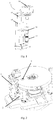
- Fig. 1 is a structural schematic of a peripheral vision acquisition system for capturing images of the wafer edge in a wafer pre-alignment apparatus according to the present invention.
- the peripheral vision acquisition system is configured essentially to capture images of the wafer edge, which are then subjected to image processing and calculation in order to obtain deviations in centering and orientation of the wafer. Based on the calculation results, centering and orientation assemblies in the wafer stage system perform compensation for the deviations.
- the peripheral vision acquisition system 1 is essentially composed of a linear array CCD camera 10, a base 11, a light source 12, a lens 13, a bracket 14 and an adjustment member 15.
- FIG. 2 schematically shows where the peripheral vision acquisition system according to the present invention is mounted. As shown in Fig. 2 , the peripheral vision acquisition system 1 is mounted along a radial pre-alignment direction (i.e., a radial direction of the wafer) at a location 3 on one side of the wafer. A channel 2 is further perforated in a moisture-tight plate in order to allow edge image acquisition for 8" wafers.
- a radial pre-alignment direction i.e., a radial direction of the wafer
- Fig. 3 shows a schematic illustration of a mark detection system in a wafer pre-alignment apparatus according to the present invention.
- the mark detection system is required to be able to: 1) search for alignment marks on the wafer surface; 2) adjust the distance from the camera (or lens) to wafer surface so that alignment marks on wafers of different thicknesses can be clearly visible; and 3) measure positional deviations of the alignment marks with respect to a geometric center of the wafer.
- the mechanics of the mark detection system are designed based on these three requirements as well as on input design constraints.
- the mark detection system 4 is essentially composed of a motion assembly 48, a focus adjustment assembly 47 and a vision assembly for mark acquisition 46.
- the motion assembly 48 is configured to drive the vision assembly for mark acquisition 46 to move radially over the wafer so that the latter can perform a search for the marks on the wafer surface.
- the focus adjustment assembly 47 is configured to drive the vision assembly for mark acquisition 46 to move along the vertical Z-direction so that a focal plane for mark detection may be adjusted to a location where clear images of the alignment marks may be captured.
- the vision assembly for mark acquisition 46 is configured for imaging of the alignment marks on the wafer and acquisition, transfer and processing of their images.
- the motion assembly 48 and the focus adjustment assembly 47 are both high-accuracy assemblies.
- the vision assembly for mark acquisition 46 is mounted on the focus adjustment assembly 47 which is, in turn, mounted on the motion assembly 48.
- the vision assembly for mark acquisition 46 comprises a point light source 44, a lens 42 and a planar array CCD camera 40.
- the motion assembly is designed to be able to travel a total length of 80 mm in which 75 mm is effective.
- the focus adjustment assembly is designed to be able to travel a total length of 8 mm in which 5 mm is effective.
- Fig. 4 is a schematic showing where the mark detection system is mounted in the wafer pre-alignment apparatus according to the present invention. As shown in Fig. 4 , the mark detection system 4 is mounted along a radial pre-alignment direction on the other side of the wafer (i.e., opposite to the peripheral vision acquisition system 1).
- the wafer stage includes an R-directional (i.e., the direction about the vertical Z-direction) motion assembly 5 and an eccentricity compensation assembly 6.
- Fig. 5 is a diagram schematically showing an area that can be imaged by the peripheral vision acquisition system and mark detection system in the wafer pre-alignment apparatus according to the present invention, which work together with each other.
- Clear images of alignment marks on a 8" or 12"wafer can be captured under the effect of the R-directional motion assembly 5 rotating about the Z-axis in cooperation with the peripheral vision acquisition system, the motion assembly of the mark detection system moving radially in cooperation with the focus adjustment assembly and the linear array CCD working together with the planar CCD array.
- the captured images can be subjected to image processing to allow higher centering and orientation accuracy of the pre-alignment process.
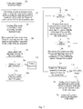
- Fig. 7 is a flow chart of a wafer pre-alignment method according to the present invention. As shown in Fig. 7 , the method includes the steps as detailed below.
- the peripheral vision acquisition system performs a coarse pre-alignment process based on captured images of the wafer edge.
- the orientation of the notch is calculated and an angle by which the wafer is to be rotated is also calculated based on positional relationships between the notch, the alignment marks and the field of view for the alignment marks.
- the wafer is rotated along the R-axis (i.e., the axis of rotation about the vertical Z-direction) so that the notch is located within the alignment field of view.
- step 704 based on mark positions suggested by the results of the pre-alignment process, the motion assembly searches for a first mark by moving radially toward the center of the wafer, wherein the maximum effective length that the motion assembly can travel is 75 mm.
- step 705 the CCD camera captures images and performs automatic focusing.
- step 706 it is determined whether an optimum focal plane is achieved. If the determination is positive, the control proceeds to step 708 in which the vision assembly for mark acquisition captures images for the first alignment mark; otherwise, the control proceeds to step 707 in which the focus adjustment assembly is moved vertically and the control loops back to step 705.
- step 709 it is checked whether any of the image captured in step 708 contains the alignment mark (i.e., the first alignment mark).
- step 714 it is determined whether the two alignment marks have been both identified. If no alignment mark is identified in step 709, the control proceeds to step 710 in which the wafer is rotated clockwise or counterclockwise along the R-axis by successive angles not exceeding 1.5 degrees, with the vision assembly for mark acquisition again capturing images for the alignment mark (i.e., the first alignment mark) after each rotation. In step 711, it is again determined whether the alignment mark has been identified. If the determination is positive, the control proceeds to step 714; otherwise, it proceeds to step 712, in which the motion assembly is moved forward and backward successively within the allowable range by increments of 1 mm, followed by the performance of step 709 after each incremental movement.
- step 713 the wafer is rotated by 180 degrees along the R-axis
- the vision assembly for mark acquisition captures images for the second alignment mark and the control loops back to step 709.
- step 715 is performed in which positional deviations of the wafer from the wafer stage are calculated based on coordinates of the first and second alignment marks.
- An R-angle is fed back to the pre-alignment system, and the coordinates of the first and second alignment marks in the coordinate system of the wafer (GWCS) are fed back to the wafer stage.
- the R-angle refers to an angle defined by the two lines each connecting an origin of the coordinate system of the wafer and one of the two alignment marks
- the coordinate system of the wafer is originated at the center of the wafer and has a Y-axis passing through a center of the plain edge portion/notch and the center of the wafer and an X-axis passing through the center of the wafer and crossing the Y-axis at right angles.
- step 716 a more accurate pre-alignment is performed on the wafer.
- step 704 in order to facilitate the search for the alignment marks, theoretic GWCS positions of the marks (determined once the marks have been formed) and measured values of eccentricity and angular deviation of the wafer obtained from the coarse pre-alignment process may be leveraged.
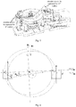
- W1 and W2 indicate the two marks MARK1 and MARK2 which are arranged in symmetry on the wafer
- N represents an origin of a coordinate system defined by the alignment marks (referred to as the "WCS coordinate system” hereinafter), wherein the origin N is located at a midpoint of a line segment connecting the two marks.
- the WCS coordinate system has a Y-axis passing through the origin N and crossing the line segment at right angles and an X-axis (horizontal) extending along the line segment.
- the direction leading from the origin toward the plain edge portion/notch of the wafer is defined as a -Y direction.
- O represents an origin of a MSCS coordinate system, wherein the MSCS coordinate system refers to a coordinate system of the mark detection system.
- a U-axis is defined by a line passing through a center of the wafer stage and a center of the mark detection system, and a V-axis is defined by a line crossing the U-axis at right angles and passing through the center of the wafer stage.
- the angle ⁇ is a rotation angle between the WCS and MSCS coordinate systems, and P indicates a center of the field of view for mark detection.
- the distance between N and O (referred to as NO) is equal to W1M or MW2'.
- the calculated rotation angle ⁇ is fed to the wafer stage system to enable the centering and orientation assemblies in the wafer stage system to perform accurate positional compensation of the wafer with respect to the wafer stage. As such compensation is known to those skilled in the art, a further description thereof is omitted herein.
- the origin O of the WSCS coordinate system is coincide with the center of the wafer stage, and the relative position between the origin N of the WCS coordinate system (i.e., the midpoint of the line segment connecting the two marks) and the center of the wafer can be determined beforehand (when the two marks are located exactly in symmetry with respect to the center of the wafer, N is coincide with the center of the wafer, and even when the two marks are not symmetric to each other with respect to the center of the wafer, a deviation of the origin N from the center of the wafer can be easily calculated).
- the two alignment marks W1 and W2 on the wafer are not symmetrical to each other, but a line passing through them also passes through the center of the wafer. That is, the two alignment marks W1 and W2 are not equidistant from the center of the wafer. Differing from Embodiment 2, after the first alignment mark W1 has been identified, the mark detection system needs to search for the second alignment mark W2 by rotating the wafer along the R-axis in accordance with this embodiment.
- Embodiment 3 differs from Embodiment 3 in that, in addition to the asymmetry of the two alignment marks W1 and W2 on the wafer, there is a significant degree of eccentricity between the wafer and the wafer stage. That is, the center of the wafer does not reside at the center of the wafer stage and is much deviated therefrom.
- the mark detection system after the first alignment mark W1 has been identified, the mark detection system always searches for the second alignment mark W2 by rotating the wafer along the R-axis, and the rest is the same as Embodiment 2.
- the actual position of the alignment mark W2 is determined based on its measured position in the GWCS coordinate system and its expected position in the WCS coordinate system.
- the positions of the two alignment marks W1 and W2 on the wafer are associated with different angles, and the line passing through them does not pass through the center of the wafer. Additionally, the two alignment marks W1 and W2 are not equidistant from the center of the wafer. In fact, the pre-alignment in this case is not substantively different from that of Embodiment 4, and a further description thereof is omitted herein.
- the positional relationships between the MSCS, GWCS and WCS coordinate systems are determinable, and more accurate alignment can be achieved based on the results of the coarse alignment.
- Embodiments 4 and 5 are presented to describe how to achieve accurate alignment in extremely rare cases in order to ensure that all wafer conditions are covered.
Landscapes
- Engineering & Computer Science (AREA)
- Computer Vision & Pattern Recognition (AREA)
- Physics & Mathematics (AREA)
- General Physics & Mathematics (AREA)
- Theoretical Computer Science (AREA)
- Quality & Reliability (AREA)
- Container, Conveyance, Adherence, Positioning, Of Wafer (AREA)
- Exposure And Positioning Against Photoresist Photosensitive Materials (AREA)
Description
- The present invention relates to the field of manufacturing of integrated circuit devices and, in particular, to an apparatus and method for pre-aligning a wafer.
- A peripheral vision acquisition system can be used to capture images of an edge (e.g., a plain edge) or a notch of a wafer. The captured images can be subjected to image processing and calculation in order to obtain deviations in centering and orientation of the wafer from a wafer stage, based on which centering and orientation assemblies in the wafer stage system can perform compensation. Wafers produced by different manufacturers may have varying wafer shapes and notch shapes and possibly different relative positional relationships between marks and the notch, and pre-alignment systems of different photolithography tools may have different centering and orientation accuracy. Consequently, wafer placement accuracy sometimes cannot meet the requirements of the photolithography tool for the next process.
-
US 2008/029715 A1 describes an alignment method of a laser beam processing machine. - In order to overcome the drawbacks of the prior art, the present invention proposes a high-accuracy apparatus and method for pre-alignment of a wafer.
- To this end, the proposed apparatus is according to
claim 1. - Additionally, the mark detection system may be configured to calculate a rotation angle and a deviation between a coordinate system of the alignment marks and the coordinate system of the mark detection system based on coordinates of the first and second alignment marks in the coordinate system of the mark detection system, and to further determine a relative positional relationship between the center of the wafer and the center of the wafer stage based on the rotation angle, the deviation and a relative positional relationship between an origin of the coordinate system of the alignment marks and the center of the wafer, wherein the coordinate system of the alignment marks has a horizontal axis defined by a line segment connecting the first and second alignment marks, the origin defined as a midpoint of the line segment connecting the first and second alignment marks and a vertical axis defined by a line passing through the origin and crossing the line at right angles.
- Additionally, the peripheral vision acquisition system may comprise a linear array CCD detector, with the mark detection system comprising a planar array CCD detector.
- Additionally, the mark detection system may comprise a motion assembly, a focus adjustment assembly and a vision assembly for mark acquisition, the motion assembly configured to drive the vision assembly for mark acquisition to search for the first or second alignment mark, the focus adjustment assembly configured to adjust a focal length of the vision assembly for mark acquisition with respect to the first or second alignment mark, the vision assembly for mark acquisition configured to capture an image of the first or second alignment mark.
- Additionally, the focus adjustment assembly may be connected to the motion assembly, with the vision assembly for mark acquisition connected to the focus adjustment assembly, wherein the motion assembly is configured to drive the focus adjustment assembly to move along a radial direction of the wafer, and the focus adjustment assembly is configured to drive the vision assembly for mark acquisition to move along a vertical direction.
- Additionally, the vision assembly for mark acquisition may comprise a point light source, a lens and a planar array CCD camera.
- The proposed method comprises the steps of: 1) providing a first alignment mark and a second alignment mark on the wafer, which are substantially symmetrical to each other with respect to a center of the wafer; 2) performing a first positional compensation for the wafer by a peripheral vision acquisition system based on a relative positional relationship of an edge or a notch of the wafer with respect to a wafer stage; 3) searching for the first and second alignment marks on the wafer and capturing images thereof by a mark detection system; 4) determining a relative positional relationship between the center of the wafer and a center of the wafer stage based on positions of the first and second alignment marks in a coordinate system of the mark detection system; and 5) performing a second positional compensation for the wafer based on the determined relative positional relationship between the center of the wafer and the center of the wafer stage, wherein the coordinate system of the mark detection system has a horizontal axis defined by a line passing through the center of the wafer stage and a center of the mark detection system and a vertical axis defined by a line crossing the horizontal axis at right angles and passing through the center of the wafer stage.
- Additionally, step 4) may comprise calculating a rotation angle and a deviation between a coordinate system of the alignment marks and the coordinate system of the mark detection system based on coordinates of the first and second alignment marks in the coordinate system of the mark detection system, and further determining a relative positional relationship between the center of the wafer and the center of the wafer stage based on the rotation angle, the deviation and a relative positional relationship between an origin of the coordinate system of the alignment marks and the center of the wafer, wherein the coordinate system of the alignment marks has a horizontal axis defined by a line segment connecting the first and second alignment marks, the origin defined as a midpoint of the line segment connecting the first and second alignment marks and a vertical axis defined by a line passing through the origin and crossing the line segment at right angles.
- Compared to the prior art, the proposed technical solution can achieve higher wafer centering and orientation accuracy and hence higher wafer placement accuracy through capturing images of the first and second alignment marks and subjecting them to calculation after coarse pre-alignment (i.e., the first positional compensation).
- The advantages of the present invention will be further understood from the following detailed description and the accompanying drawings.
-
Fig. 1 is a structural schematic of a peripheral vision acquisition system for capturing images of the edge of a wafer in a wafer pre-alignment apparatus according to the present invention. -
Fig. 2 schematically shows where the peripheral vision acquisition system according to the present invention is mounted. -
Fig. 3 shows a schematic illustration of a mark detection system in the wafer pre-alignment apparatus according to the present invention. -
Fig. 4 is a schematic showing where the mark detection system in the wafer pre-alignment apparatus according to the present invention is mounted. -
Fig. 5 is a diagram schematically showing an area that can be imaged by the peripheral vision acquisition system and mark detection system in the wafer pre-alignment apparatus according to the present invention, which work together with each other. -
Fig. 6 is a schematic illustration of a use scenario of the wafer pre-alignment apparatus according to the present invention. -
Fig. 7 is a flow chart of a wafer pre-alignment method according to the present invention. - Specific embodiments of the present invention will be described in detail with reference to the accompanying drawings.
- The conventional approaches can only achieve coarse pre-alignment by scanning the wafer edge and notch. According to the present invention, higher wafer centering and orientation accuracy can be achieved by performing a further alignment using two marks subsequent to the coarse pre-alignment so that the resulting wafer placement accuracy is more likely to meet the requirements.
- In order to improve the centering and orientation accuracy of a wafer to be placed on a wafer stage, the wafer is pre-aligned based on images of its edges and then calibrated by a mark detection system using alignment marks, in order to achieve higher placement accuracy.
- To this end, the mark detection system is designed to be able to: 1) more accurately align the alignment marks on the wafer to be placed on the wafer stage into an alignment field of view so as to avoid excessive errors in wafer placement accuracy caused by variations in mark geometry, size and position between different wafers; 2) act as measuring device to measure coordinate deviations of the alignment marks with respect to the wafer geometry; and 3) calculate an angular deviation of the positions of the alignment marks in a coordinate system of the wafer from their positions in a coordinate system of the mark detection system through comparing their expected and measured positions in the coordinate system of the mark detection system.
- Measurement data obtained by the mark detection system are used for positional compensation for the wafer so that it is placed successfully on the wafer stage with sufficient centering and orientation accuracy.
-
Fig. 1 is a structural schematic of a peripheral vision acquisition system for capturing images of the wafer edge in a wafer pre-alignment apparatus according to the present invention. The peripheral vision acquisition system is configured essentially to capture images of the wafer edge, which are then subjected to image processing and calculation in order to obtain deviations in centering and orientation of the wafer. Based on the calculation results, centering and orientation assemblies in the wafer stage system perform compensation for the deviations. As shown inFig. 1 , the peripheralvision acquisition system 1 is essentially composed of a lineararray CCD camera 10, abase 11, alight source 12, alens 13, abracket 14 and anadjustment member 15. Adjusting theadjustment member 15 can ensure a sufficient distance L from a center of thelens 13 to an inner surface of thebracket 14 for switching from an 8" wafer to a 12" one.Fig. 2 schematically shows where the peripheral vision acquisition system according to the present invention is mounted. As shown inFig. 2 , the peripheralvision acquisition system 1 is mounted along a radial pre-alignment direction (i.e., a radial direction of the wafer) at alocation 3 on one side of the wafer. Achannel 2 is further perforated in a moisture-tight plate in order to allow edge image acquisition for 8" wafers. -
Fig. 3 shows a schematic illustration of a mark detection system in a wafer pre-alignment apparatus according to the present invention. As shown inFig. 3 , the mark detection system is required to be able to: 1) search for alignment marks on the wafer surface; 2) adjust the distance from the camera (or lens) to wafer surface so that alignment marks on wafers of different thicknesses can be clearly visible; and 3) measure positional deviations of the alignment marks with respect to a geometric center of the wafer. The mechanics of the mark detection system are designed based on these three requirements as well as on input design constraints. - As shown in
Fig. 3 , themark detection system 4 is essentially composed of amotion assembly 48, afocus adjustment assembly 47 and a vision assembly formark acquisition 46. Themotion assembly 48 is configured to drive the vision assembly formark acquisition 46 to move radially over the wafer so that the latter can perform a search for the marks on the wafer surface. Thefocus adjustment assembly 47 is configured to drive the vision assembly formark acquisition 46 to move along the vertical Z-direction so that a focal plane for mark detection may be adjusted to a location where clear images of the alignment marks may be captured. The vision assembly formark acquisition 46 is configured for imaging of the alignment marks on the wafer and acquisition, transfer and processing of their images. Themotion assembly 48 and thefocus adjustment assembly 47 are both high-accuracy assemblies. The vision assembly formark acquisition 46 is mounted on thefocus adjustment assembly 47 which is, in turn, mounted on themotion assembly 48. - The vision assembly for
mark acquisition 46 comprises apoint light source 44, alens 42 and a planararray CCD camera 40. In order to be able to handle both 200-mm and 300-mm wafers, the motion assembly is designed to be able to travel a total length of 80 mm in which 75 mm is effective. The focus adjustment assembly is designed to be able to travel a total length of 8 mm in which 5 mm is effective. -
Fig. 4 is a schematic showing where the mark detection system is mounted in the wafer pre-alignment apparatus according to the present invention. As shown inFig. 4 , themark detection system 4 is mounted along a radial pre-alignment direction on the other side of the wafer (i.e., opposite to the peripheral vision acquisition system 1). The wafer stage includes an R-directional (i.e., the direction about the vertical Z-direction)motion assembly 5 and aneccentricity compensation assembly 6. -
Fig. 5 is a diagram schematically showing an area that can be imaged by the peripheral vision acquisition system and mark detection system in the wafer pre-alignment apparatus according to the present invention, which work together with each other. Clear images of alignment marks on a 8" or 12"wafer can be captured under the effect of the R-directional motion assembly 5 rotating about the Z-axis in cooperation with the peripheral vision acquisition system, the motion assembly of the mark detection system moving radially in cooperation with the focus adjustment assembly and the linear array CCD working together with the planar CCD array. The captured images can be subjected to image processing to allow higher centering and orientation accuracy of the pre-alignment process. -
Fig. 7 is a flow chart of a wafer pre-alignment method according to the present invention. As shown inFig. 7 , the method includes the steps as detailed below. Instep 701, the peripheral vision acquisition system performs a coarse pre-alignment process based on captured images of the wafer edge. Instep 702, the orientation of the notch is calculated and an angle by which the wafer is to be rotated is also calculated based on positional relationships between the notch, the alignment marks and the field of view for the alignment marks. Instep 703, the wafer is rotated along the R-axis (i.e., the axis of rotation about the vertical Z-direction) so that the notch is located within the alignment field of view. Instep 704, based on mark positions suggested by the results of the pre-alignment process, the motion assembly searches for a first mark by moving radially toward the center of the wafer, wherein the maximum effective length that the motion assembly can travel is 75 mm. Instep 705, the CCD camera captures images and performs automatic focusing. Instep 706, it is determined whether an optimum focal plane is achieved. If the determination is positive, the control proceeds to step 708 in which the vision assembly for mark acquisition captures images for the first alignment mark; otherwise, the control proceeds to step 707 in which the focus adjustment assembly is moved vertically and the control loops back tostep 705. Instep 709, it is checked whether any of the image captured instep 708 contains the alignment mark (i.e., the first alignment mark). If the alignment mark is identified, the control proceeds to step 714 in which it is determined whether the two alignment marks have been both identified. If no alignment mark is identified instep 709, the control proceeds to step 710 in which the wafer is rotated clockwise or counterclockwise along the R-axis by successive angles not exceeding 1.5 degrees, with the vision assembly for mark acquisition again capturing images for the alignment mark (i.e., the first alignment mark) after each rotation. Instep 711, it is again determined whether the alignment mark has been identified. If the determination is positive, the control proceeds to step 714; otherwise, it proceeds to step 712, in which the motion assembly is moved forward and backward successively within the allowable range by increments of 1 mm, followed by the performance ofstep 709 after each incremental movement. If the first mark has been identified with the second mark having been not, then the control proceeds to step 713 in which the wafer is rotated by 180 degrees along the R-axis, the vision assembly for mark acquisition captures images for the second alignment mark and the control loops back tostep 709. Once both alignment marks have been found instep 714,step 715 is performed in which positional deviations of the wafer from the wafer stage are calculated based on coordinates of the first and second alignment marks. An R-angle is fed back to the pre-alignment system, and the coordinates of the first and second alignment marks in the coordinate system of the wafer (GWCS) are fed back to the wafer stage. Here, the R-angle refers to an angle defined by the two lines each connecting an origin of the coordinate system of the wafer and one of the two alignment marks, and the coordinate system of the wafer is originated at the center of the wafer and has a Y-axis passing through a center of the plain edge portion/notch and the center of the wafer and an X-axis passing through the center of the wafer and crossing the Y-axis at right angles. Instep 716, a more accurate pre-alignment is performed on the wafer. - In
step 704, in order to facilitate the search for the alignment marks, theoretic GWCS positions of the marks (determined once the marks have been formed) and measured values of eccentricity and angular deviation of the wafer obtained from the coarse pre-alignment process may be leveraged. - In order to fully explain the present invention, an assumed basic scenario for high-accuracy pre-alignment is described below.
- Assuming there is only a small degree of eccentricity of the wafer with respect to the wafer stage and the two marks MARK1 and MARK2 are arranged in symmetry on the wafer, and thus it is not necessary for the mark detection system to search for MARK1 and MARK2 by stepwise rotation of the wafer about the R-axis. As shown in
Fig. 6 , which is a schematic illustration of the use scenario of the wafer pre-alignment apparatus of the present invention, W1 and W2 indicate the two marks MARK1 and MARK2 which are arranged in symmetry on the wafer, and N represents an origin of a coordinate system defined by the alignment marks (referred to as the "WCS coordinate system" hereinafter), wherein the origin N is located at a midpoint of a line segment connecting the two marks. The WCS coordinate system has a Y-axis passing through the origin N and crossing the line segment at right angles and an X-axis (horizontal) extending along the line segment. The direction leading from the origin toward the plain edge portion/notch of the wafer is defined as a -Y direction. The marks MARK1 and MARK2 have the same radius, i.e., W1N=W2N. O represents an origin of a MSCS coordinate system, wherein the MSCS coordinate system refers to a coordinate system of the mark detection system. A U-axis is defined by a line passing through a center of the wafer stage and a center of the mark detection system, and a V-axis is defined by a line crossing the U-axis at right angles and passing through the center of the wafer stage. W2' denotes a position of MARK2 after the wafer is rotated by 180 degrees about O, and M represents a midpoint of the segment W1W2'. Therefore, we can easily obtain MO=W1N=W2N. The angle α is a rotation angle between the WCS and MSCS coordinate systems, and P indicates a center of the field of view for mark detection. The distance between N and O (referred to as NO) is equal to W1M or MW2'.
- where, Y(W1) denotes the Y-coordinate value of the alignment mark W1 in the MSCS coordinate system, and
- Y(W2') represents the Y-coordinate value of the alignment mark W2 after it is rotated by 180 degrees in the MSCS coordinate system.
- The calculated rotation angle α is fed to the wafer stage system to enable the centering and orientation assemblies in the wafer stage system to perform accurate positional compensation of the wafer with respect to the wafer stage. As such compensation is known to those skilled in the art, a further description thereof is omitted herein.
- It can be easily appreciated that the origin O of the WSCS coordinate system is coincide with the center of the wafer stage, and the relative position between the origin N of the WCS coordinate system (i.e., the midpoint of the line segment connecting the two marks) and the center of the wafer can be determined beforehand (when the two marks are located exactly in symmetry with respect to the center of the wafer, N is coincide with the center of the wafer, and even when the two marks are not symmetric to each other with respect to the center of the wafer, a deviation of the origin N from the center of the wafer can be easily calculated). Therefore, once the positional relationship between the points O and N is determined, it is easy to derive the positional relationship between O and the center of the wafer, based on which the center of the wafer can be adjusted into coincidence with the center of the wafer stage by the wafer stage system.
- In this embodiment, the two alignment marks W1 and W2 on the wafer are not symmetrical to each other, but a line passing through them also passes through the center of the wafer. That is, the two alignment marks W1 and W2 are not equidistant from the center of the wafer. Differing from
Embodiment 2, after the first alignment mark W1 has been identified, the mark detection system needs to search for the second alignment mark W2 by rotating the wafer along the R-axis in accordance with this embodiment. - This embodiment differs from
Embodiment 3 in that, in addition to the asymmetry of the two alignment marks W1 and W2 on the wafer, there is a significant degree of eccentricity between the wafer and the wafer stage. That is, the center of the wafer does not reside at the center of the wafer stage and is much deviated therefrom. Compared toEmbodiment 3, after the first alignment mark W1 has been identified, the mark detection system always searches for the second alignment mark W2 by rotating the wafer along the R-axis, and the rest is the same asEmbodiment 2. The only difference is that the actual position of the alignment mark W2 is determined based on its measured position in the GWCS coordinate system and its expected position in the WCS coordinate system. - In this embodiment, the positions of the two alignment marks W1 and W2 on the wafer are associated with different angles, and the line passing through them does not pass through the center of the wafer. Additionally, the two alignment marks W1 and W2 are not equidistant from the center of the wafer. In fact, the pre-alignment in this case is not substantively different from that of
Embodiment 4, and a further description thereof is omitted herein. - According to these embodiments, the positional relationships between the MSCS, GWCS and WCS coordinate systems are determinable, and more accurate alignment can be achieved based on the results of the coarse alignment.
- In general cases, the deviations of the wafer with respect to the wafer stage and positional deviations of the marks are not significant after the coarse alignment is performed, and accurate alignment could be achieved in accordance with
Embodiments - Disclosed herein are merely several preferred particular embodiments of the present invention, which are intended to explain the subject matter of the invention rather than limit the scope thereof. All embodiments made by those skilled in the art by means of logical analysis, reference or limited experimentation based on the teachings of the invention are embraced within the scope of the invention. The invention is defined by the appended claims.
Claims (8)
- A pre-alignment apparatus for a wafer, comprising:a wafer to be pre-aligned;a wafer stage for supporting the wafer, wherein a first alignment mark (W1) and a second alignment mark (W2) are provided on the wafer such that the first and second alignment marks (W1, W2) are substantially symmetrical to each other with respect to a center of the wafer;a peripheral vision acquisition system (1), configured to perform a first positional compensation for the wafer based on a relative positional relationship of an edge or a notch of the wafer with respect to the wafer stage;characterized in that the pre-alignment apparatus further comprises a mark detection system (4), configured to capture images of the first and second alignment marks (W1, W2), and perform a second positional compensation for the wafer by determining a relative positional relationship of the center of the wafer with respect to a center of the wafer stage based on positions of the first and second alignment marks (W1, W2) in a coordinate system of the mark detection system (4),the peripheral vision acquisition system (1) and the mark detection system (4) are located on opposite sides of the wafer along a radial direction of the wafer, andthe coordinate system of the mark detection system has a horizontal axis defined by a line passing through the center of the wafer stage and a center of the mark detection system (4) and a vertical axis defined by a line crossing the horizontal axis at right angles and passing through the center of the wafer stage.
- The pre-alignment apparatus for a wafer as recited in claim 1, wherein the mark detection system is configured to calculate a rotation angle and a deviation between a coordinate system of the alignment marks and the coordinate system of the mark detection system based on coordinates of the first and second alignment marks in the coordinate system of the mark detection system (4), and to further determine a relative positional relationship between the center of the wafer and the center of the wafer stage based on the rotation angle, the deviation and a relative positional relationship between an origin of the coordinate system of the alignment marks and the center of the wafer, and wherein the coordinate system of the alignment marks has a horizontal axis defined by a line segment connecting the first and second alignment marks, the origin defined as a midpoint of the line segment connecting the first and second alignment marks and a vertical axis defined by a line passing through the origin and crossing the line segment at right angles.
- The pre-alignment apparatus for a wafer as recited in claim 1, wherein the peripheral vision acquisition system (1) comprises a linear array CCD detector (10), and wherein the mark detection system (4) comprises a planar array CCD detector (40).
- The pre-alignment apparatus for a wafer as recited in claim 1, wherein the mark detection system (4) comprises a motion assembly (48), a focus adjustment assembly (47) and a vision assembly for mark acquisition (46), the motion assembly (48) configured to drive the vision assembly for mark acquisition (46) to search for the first or second alignment mark, the focus adjustment assembly (47) configured to adjust a focal length of the vision assembly for mark acquisition (46) with respect to the first or second alignment mark, the vision assembly for mark acquisition (46) configured to capture an image of the first or second alignment mark.
- The pre-alignment apparatus for a wafer as recited in claim 4, wherein the focus adjustment assembly (47) is connected to the motion assembly (48), and the vision assembly for mark acquisition (46) is connected to the focus adjustment assembly (47), the motion assembly (48) configured to drive the focus adjustment assembly (47) to move along a radial direction of the wafer, the focus adjustment assembly (47) configured to drive the vision assembly for mark acquisition (46) to move along a vertical direction.
- The pre-alignment apparatus for a wafer as recited in claim 4, wherein the vision assembly for mark acquisition (46) comprises a point light source (44), a lens (42) and a planar array CCD camera (40).
- A pre-alignment method for a wafer, comprising:step 1, providing, on the wafer, a first alignment mark (W1) and a second alignment mark (W2) that are substantially symmetrical to each other with respect to a center of the wafer;step 2, performing a first positional compensation for the wafer by a peripheral vision acquisition system (1) based on a relative positional relationship of an edge or a notch of the wafer with respect to a wafer stage;step 3, searching for the first and second alignment marks (W1, W2) on the wafer and capturing images thereof by a mark detection system (4);step 4, determining a relative positional relationship between the center of the wafer and a center of the wafer stage based on positions of the first and second alignment marks (W1, W2) in a coordinate system of the mark detection system; andstep 5, performing a second positional compensation for the wafer based on the determined relative positional relationship between the center of the wafer and the center of the wafer stage,wherein the coordinate system of the mark detection system (4) has a horizontal axis defined by a line passing through the center of the wafer stage and a center of the mark detection system (4) and a vertical axis defined by a line crossing the horizontal axis at right angles and passing through the center of the wafer stage.
- The pre-alignment method for a wafer as recited in claim 7, wherein step 4) comprises calculating a rotation angle and a deviation between a coordinate system of the alignment marks and the coordinate system of the mark detection system based on coordinates of the first and second alignment marks in the coordinate system of the mark detection system (4), and further determining a relative positional relationship between the center of the wafer and the center of the wafer stage based on the rotation angle, the deviation and a relative positional relationship between an origin of the coordinate system of the alignment marks and the center of the wafer, and wherein the coordinate system of the alignment marks has a horizontal axis defined by a line segment connecting the first and second alignment marks, the origin defined as a midpoint of the line segment connecting the first and second alignment marks and a vertical axis defined by a line passing through the origin and crossing the line segment at right angles.
Applications Claiming Priority (2)
| Application Number | Priority Date | Filing Date | Title |
|---|---|---|---|
| CN201510203515.6A CN106158715B (en) | 2015-04-24 | 2015-04-24 | Pre-alignment device and method for wafer |
| PCT/CN2016/079979 WO2016169511A1 (en) | 2015-04-24 | 2016-04-22 | Pre-alignment device and method for wafer |
Publications (3)
| Publication Number | Publication Date |
|---|---|
| EP3288063A1 EP3288063A1 (en) | 2018-02-28 |
| EP3288063A4 EP3288063A4 (en) | 2018-12-05 |
| EP3288063B1 true EP3288063B1 (en) | 2020-02-26 |
Family
ID=57144391
Family Applications (1)
| Application Number | Title | Priority Date | Filing Date |
|---|---|---|---|
| EP16782658.5A Active EP3288063B1 (en) | 2015-04-24 | 2016-04-22 | Pre-alignment device and method for wafer |
Country Status (8)
| Country | Link |
|---|---|
| US (1) | US10276417B2 (en) |
| EP (1) | EP3288063B1 (en) |
| JP (1) | JP6530825B2 (en) |
| KR (1) | KR102048301B1 (en) |
| CN (1) | CN106158715B (en) |
| SG (1) | SG11201708695PA (en) |
| TW (1) | TW201715638A (en) |
| WO (1) | WO2016169511A1 (en) |
Families Citing this family (39)
| Publication number | Priority date | Publication date | Assignee | Title |
|---|---|---|---|---|
| JP6423678B2 (en) * | 2014-10-07 | 2018-11-14 | 東京エレクトロン株式会社 | Substrate inspection apparatus and control method thereof |
| CN105182702B (en) * | 2015-10-30 | 2017-08-11 | 京东方科技集团股份有限公司 | Alignment mark method for searching, display base plate and display device |
| WO2018152202A1 (en) * | 2017-02-14 | 2018-08-23 | Massachusetts Institute Of Technology | Systems and methods for automated microscopy |
| CN108735644A (en) * | 2017-04-25 | 2018-11-02 | 北京中科信电子装备有限公司 | A kind of method of silicon chip orientation and position compensation |
| CN109451763B (en) * | 2018-05-16 | 2019-11-08 | 长江存储科技有限责任公司 | Method and system for wafer bonding alignment compensation |
| CN108615699B (en) * | 2018-05-29 | 2023-11-07 | 深圳信息职业技术学院 | A wafer alignment system and method and an optical imaging device for wafer alignment |
| CN110488751B (en) * | 2018-08-29 | 2022-08-19 | 中山大学 | Graphite tray visual positioning system of automatic process line |
| IL282349B2 (en) | 2018-10-23 | 2025-04-01 | Asml Netherlands Bv | Method and apparatus for adaptive alignment |
| CN109540904A (en) * | 2018-12-12 | 2019-03-29 | 华侨大学 | A kind of detection of substrate surface gross imperfection and categorizing system |
| WO2020181482A1 (en) * | 2019-03-12 | 2020-09-17 | Texas Instruments Incorporated | Method to improve nikon wafer loader repeatability |
| US11352698B2 (en) * | 2019-04-25 | 2022-06-07 | Samsung Electronics Co., Ltd. | Atomic layer deposition apparatus and methods of fabricating semiconductor devices using the same |
| CN110224052B (en) * | 2019-05-28 | 2024-02-06 | 深圳新益昌科技股份有限公司 | A double-swing arm crystal-bonding device for LED crystal-bonding and its crystal-bonding method |
| CN110729216A (en) * | 2019-10-21 | 2020-01-24 | 华虹半导体(无锡)有限公司 | Wafer position detection device and wafer position detection method |
| KR102953169B1 (en) | 2019-11-13 | 2026-04-15 | 가부시키가이샤 에무씨케이 | Return device and return method |
| CN113066746B (en) * | 2020-01-02 | 2022-03-22 | 长鑫存储技术有限公司 | Pre-alignment device and pre-alignment method applied to same |
| US12027400B2 (en) * | 2020-05-26 | 2024-07-02 | Asm Ip Holding B.V. | Automatic system calibration for wafer handling |
| CN111952230B (en) * | 2020-09-01 | 2021-03-16 | 无锡卓海科技有限公司 | Transparent wafer edge extraction method of pre-alignment machine |
| CN114695225A (en) * | 2020-12-31 | 2022-07-01 | 上海微电子装备(集团)股份有限公司 | Wafer pre-alignment device and wafer pre-alignment method |
| CN112838038B (en) * | 2021-02-02 | 2024-05-28 | 沈阳芯源微电子设备股份有限公司 | Alignment method and alignment system |
| US11978677B2 (en) * | 2021-06-24 | 2024-05-07 | Taiwan Semiconductor Manufacturing Co., Ltd. | Wafer positioning method and apparatus |
| CN113251929B (en) * | 2021-06-28 | 2021-10-29 | 深圳中科飞测科技股份有限公司 | Detection equipment and detection method, detection system and storage medium |
| CN114464564B (en) * | 2022-01-18 | 2026-03-13 | 北京华卓精科科技股份有限公司 | A wafer alignment method and apparatus |
| CN116504698A (en) * | 2022-01-19 | 2023-07-28 | 上海凯世通半导体股份有限公司 | Semiconductor wafer alignment device, alignment method and alignment system |
| CN116504666B (en) * | 2022-01-19 | 2026-06-09 | 上海凯世通半导体股份有限公司 | Semiconductor wafer position detection device, detection method and detection system |
| JP7830970B2 (en) * | 2022-02-02 | 2026-03-17 | オムロン株式会社 | Method for measuring the amount of deviation, measuring apparatus, and program |
| CN114474440B (en) * | 2022-03-16 | 2023-03-10 | 江苏京创先进电子科技有限公司 | Method for controlling adjustment precision of fine adjustment device |
| CN114664721B (en) * | 2022-03-21 | 2025-12-05 | 北京半导体专用设备研究所(中国电子科技集团公司第四十五研究所) | A wafer positioning pre-alignment method, electronic device and wafer transfer system |
| CN114823454B (en) * | 2022-05-16 | 2026-01-23 | 北京华卓精科科技股份有限公司 | Wafer alignment device and alignment method |
| US20260050227A1 (en) * | 2022-09-20 | 2026-02-19 | Applied Materials, Inc. | On tool metrology scheme for advanced packaging |
| CN115831845B (en) * | 2022-12-21 | 2026-06-02 | 芯联集成电路制造股份有限公司 | Wafer prealignment apparatus and wafer prealignment method |
| CN116422543B (en) * | 2023-06-15 | 2023-09-08 | 苏州希盟科技股份有限公司 | Dispensing control method, device, equipment and medium based on space plane |
| CN116995011B (en) * | 2023-08-16 | 2024-01-09 | 泓浒(苏州)半导体科技有限公司 | Calibration method and calibration system for loading and unloading wafer carrier |
| TWI846579B (en) * | 2023-08-29 | 2024-06-21 | 三和技研股份有限公司 | Wafer positioning device and method |
| CN116878386B (en) * | 2023-09-06 | 2023-12-08 | 北京华卓精科科技股份有限公司 | Calibration method and calibration device for up-down alignment visual device |
| CN117012689B (en) * | 2023-09-26 | 2023-12-15 | 天津中科晶禾电子科技有限责任公司 | Wafer alignment device and method |
| CN118983255B (en) * | 2024-08-06 | 2025-10-24 | 三河建华高科有限责任公司 | A high-precision wafer pre-alignment mechanism |
| US20260161102A1 (en) * | 2024-12-10 | 2026-06-11 | Onto Innovation Inc. | Device alignment for correcting substrate angle |
| CN119890118B (en) * | 2024-12-27 | 2025-10-31 | 广东华矽半导体设备有限公司 | A vision-based wafer pre-alignment system and method |
| CN119910568A (en) * | 2025-01-22 | 2025-05-02 | 睿励科学仪器(上海)有限公司 | Wafer positioning method, system, chemical mechanical polishing equipment and storage medium |
Family Cites Families (32)
| Publication number | Priority date | Publication date | Assignee | Title |
|---|---|---|---|---|
| US3930684A (en) * | 1971-06-22 | 1976-01-06 | Lasch Jr Cecil A | Automatic wafer feeding and pre-alignment apparatus and method |
| US4461567A (en) * | 1979-12-20 | 1984-07-24 | Censor Patent- Und Versuchs-Anstalt | Method of and apparatus for the positioning of disk-shaped workpieces, particularly semiconductor wafers |
| US4376581A (en) * | 1979-12-20 | 1983-03-15 | Censor Patent- Und Versuchs-Anstalt | Method of positioning disk-shaped workpieces, preferably semiconductor wafers |
| JP2675307B2 (en) * | 1987-08-28 | 1997-11-12 | 株式会社日立製作所 | Preliner equipment |
| US5044752A (en) * | 1989-06-30 | 1991-09-03 | General Signal Corporation | Apparatus and process for positioning wafers in receiving devices |
| JP2949528B2 (en) * | 1991-03-13 | 1999-09-13 | 東京エレクトロン株式会社 | Method and apparatus for detecting center position of wafer |
| JP2000228347A (en) * | 1999-02-08 | 2000-08-15 | Nikon Corp | Positioning method and exposure apparatus |
| US6624433B2 (en) * | 1994-02-22 | 2003-09-23 | Nikon Corporation | Method and apparatus for positioning substrate and the like |
| US5563798A (en) * | 1994-04-05 | 1996-10-08 | Applied Materials, Inc. | Wafer positioning system |
| JP2000035676A (en) * | 1998-05-15 | 2000-02-02 | Nippon Seiko Kk | Division sequential proximity exposure system |
| US6237393B1 (en) * | 1999-07-30 | 2001-05-29 | International Business Machines Corporation | Wafer center alignment device and method of wafer alignment |
| US7008802B2 (en) * | 2001-05-29 | 2006-03-07 | Asm America, Inc. | Method and apparatus to correct water drift |
| JP2002365809A (en) * | 2001-06-12 | 2002-12-18 | Nsk Ltd | Division sequential exposure system |
| TW594431B (en) * | 2002-03-01 | 2004-06-21 | Asml Netherlands Bv | Calibration methods, calibration substrates, lithographic apparatus and device manufacturing methods |
| US7067763B2 (en) * | 2002-05-17 | 2006-06-27 | Gsi Group Corporation | High speed, laser-based marking method and system for producing machine readable marks on workpieces and semiconductor devices with reduced subsurface damage produced thereby |
| JP2004281983A (en) * | 2003-03-19 | 2004-10-07 | Toray Ind Inc | Positioning device and positioning method, coating device and coating method |
| KR101025632B1 (en) * | 2004-11-30 | 2011-03-30 | 가부시키가이샤 야스카와덴키 | Alignment device |
| US7706908B2 (en) * | 2005-02-22 | 2010-04-27 | Oc Oerlikon Balzers Ag | Method for positioning a wafer |
| JP5000944B2 (en) * | 2006-08-02 | 2012-08-15 | 株式会社ディスコ | Alignment method for laser processing equipment |
| JP5239220B2 (en) * | 2007-06-12 | 2013-07-17 | 株式会社ニコン | Wafer positioning apparatus and wafer bonding apparatus having the same |
| CN101216686B (en) | 2008-01-10 | 2010-08-25 | 上海微电子装备有限公司 | A wafer pre-alignment platform and a wafer pre-alignment method using the same |
| US8334520B2 (en) * | 2008-10-24 | 2012-12-18 | Hitachi High-Technologies Corporation | Charged particle beam apparatus |
| JP2011021999A (en) * | 2009-07-15 | 2011-02-03 | Kyodo Design & Planning Corp | Substrate inspecting apparatus |
| JP5524550B2 (en) * | 2009-09-15 | 2014-06-18 | 株式会社ニコン | Substrate bonding apparatus, substrate bonding method, and device manufacturing method |
| JP2013026383A (en) * | 2011-07-20 | 2013-02-04 | Dainippon Screen Mfg Co Ltd | Alignment device, alignment method, and drawing device |
| JP5836223B2 (en) * | 2011-12-02 | 2015-12-24 | 株式会社神戸製鋼所 | Rotation deviation amount measuring device for bonding substrate, method for measuring rotation deviation amount of bonding substrate, and manufacturing method of bonding substrate |
| CN202661393U (en) * | 2012-03-12 | 2013-01-09 | 苏州爱特盟光电有限公司 | Nanoscale and microscale detector for measuring microscopic size of integrated circuit |
| JP6502846B2 (en) * | 2012-06-06 | 2019-04-17 | エーファウ・グループ・エー・タルナー・ゲーエムベーハー | Apparatus and method for determining registration error |
| JP5516684B2 (en) * | 2012-10-02 | 2014-06-11 | 株式会社ニコン | Wafer bonding method, positioning method, and semiconductor manufacturing apparatus having the same |
| SG2014014054A (en) * | 2013-06-17 | 2014-10-30 | Ev Group E Thallner Gmbh | Device and Method for Alignment of substrates |
| CN103604815B (en) * | 2013-11-26 | 2016-01-13 | 上海海事大学 | Chip glass pick-up unit and scaling method |
| CN104536186B (en) * | 2015-01-13 | 2017-12-08 | 合肥鑫晟光电科技有限公司 | A kind of identification device and alignment system |
-
2015
- 2015-04-24 CN CN201510203515.6A patent/CN106158715B/en active Active
-
2016
- 2016-04-22 KR KR1020177033877A patent/KR102048301B1/en active Active
- 2016-04-22 US US15/568,657 patent/US10276417B2/en active Active
- 2016-04-22 WO PCT/CN2016/079979 patent/WO2016169511A1/en not_active Ceased
- 2016-04-22 JP JP2017555261A patent/JP6530825B2/en active Active
- 2016-04-22 SG SG11201708695PA patent/SG11201708695PA/en unknown
- 2016-04-22 TW TW105112591A patent/TW201715638A/en unknown
- 2016-04-22 EP EP16782658.5A patent/EP3288063B1/en active Active
Non-Patent Citations (1)
| Title |
|---|
| None * |
Also Published As
| Publication number | Publication date |
|---|---|
| KR102048301B1 (en) | 2019-11-25 |
| JP2018513563A (en) | 2018-05-24 |
| CN106158715B (en) | 2021-04-02 |
| SG11201708695PA (en) | 2017-11-29 |
| EP3288063A1 (en) | 2018-02-28 |
| WO2016169511A1 (en) | 2016-10-27 |
| JP6530825B2 (en) | 2019-06-12 |
| CN106158715A (en) | 2016-11-23 |
| US10276417B2 (en) | 2019-04-30 |
| TW201715638A (en) | 2017-05-01 |
| EP3288063A4 (en) | 2018-12-05 |
| KR20170137927A (en) | 2017-12-13 |
| US20180151400A1 (en) | 2018-05-31 |
Similar Documents
| Publication | Publication Date | Title |
|---|---|---|
| US10276417B2 (en) | Pre-alignment device and method for wafer | |
| CN114695225A (en) | Wafer pre-alignment device and wafer pre-alignment method | |
| US10197923B2 (en) | Exposure device and out-of-focus and tilt error compensation method | |
| US20090196527A1 (en) | Calibration method of image planar coordinate system for high-precision image measurement system | |
| US10197390B2 (en) | Pre-alignment measurement device and method | |
| CN114820761B (en) | XY direction included angle measurement and motion compensation method based on image microscopic scanning platform | |
| CN108805940B (en) | Method for tracking and positioning zoom camera in zooming process | |
| KR20190037112A (en) | Inspection method and inspection apparatus | |
| JP4037947B2 (en) | Object alignment method | |
| US20240265569A1 (en) | Positioning device, mounting device, positioning method, and method for manufacturing electronic component | |
| US20170328807A1 (en) | Focusing state measuring apparatus | |
| CN120280383B (en) | Wafer edge scanning method and device | |
| CN119108317B (en) | Wafer edge searching method and device | |
| JPH11326229A (en) | Foreign matter inspection device | |
| JP3774320B2 (en) | Wafer position grasping method, exposure method, and exposure apparatus | |
| CN112308919A (en) | Method and device for correcting clamping position of chip in clamp | |
| CN114111578B (en) | A method for automatically determining the position and posture of large-diameter components | |
| US7480404B2 (en) | Method and system for positioning articles with respect to a processing tool | |
| KR102823184B1 (en) | Docking System for Shaft Axis Using 2D Vision | |
| CN121522976B (en) | Alignment leveling system, alignment leveling method and lithography equipment | |
| EP4492808A1 (en) | Focal length measuring device and method | |
| KR20060014346A (en) | Micro Dimension Meter | |
| JP3250537B2 (en) | Positioning method and apparatus used for the method | |
| JP3340199B2 (en) | Aspherical lens eccentricity measuring device | |
| CN110530295B (en) | Tool and method for detecting perpendicularity of motion platform |
Legal Events
| Date | Code | Title | Description |
|---|---|---|---|
| STAA | Information on the status of an ep patent application or granted ep patent |
Free format text: STATUS: THE INTERNATIONAL PUBLICATION HAS BEEN MADE |
|
| PUAI | Public reference made under article 153(3) epc to a published international application that has entered the european phase |
Free format text: ORIGINAL CODE: 0009012 |
|
| STAA | Information on the status of an ep patent application or granted ep patent |
Free format text: STATUS: REQUEST FOR EXAMINATION WAS MADE |
|
| 17P | Request for examination filed |
Effective date: 20171123 |
|
| AK | Designated contracting states |
Kind code of ref document: A1 Designated state(s): AL AT BE BG CH CY CZ DE DK EE ES FI FR GB GR HR HU IE IS IT LI LT LU LV MC MK MT NL NO PL PT RO RS SE SI SK SM TR |
|
| AX | Request for extension of the european patent |
Extension state: BA ME |
|
| DAV | Request for validation of the european patent (deleted) | ||
| DAX | Request for extension of the european patent (deleted) | ||
| A4 | Supplementary search report drawn up and despatched |
Effective date: 20181102 |
|
| RIC1 | Information provided on ipc code assigned before grant |
Ipc: G06T 7/73 20170101ALI20181026BHEP Ipc: G06T 7/00 20170101ALI20181026BHEP Ipc: H01L 21/687 20060101ALI20181026BHEP Ipc: H01L 23/544 20060101ALI20181026BHEP Ipc: H01L 21/68 20060101AFI20181026BHEP |
|
| GRAP | Despatch of communication of intention to grant a patent |
Free format text: ORIGINAL CODE: EPIDOSNIGR1 |
|
| STAA | Information on the status of an ep patent application or granted ep patent |
Free format text: STATUS: GRANT OF PATENT IS INTENDED |
|
| INTG | Intention to grant announced |
Effective date: 20191004 |
|
| GRAS | Grant fee paid |
Free format text: ORIGINAL CODE: EPIDOSNIGR3 |
|
| GRAA | (expected) grant |
Free format text: ORIGINAL CODE: 0009210 |
|
| STAA | Information on the status of an ep patent application or granted ep patent |
Free format text: STATUS: THE PATENT HAS BEEN GRANTED |
|
| AK | Designated contracting states |
Kind code of ref document: B1 Designated state(s): AL AT BE BG CH CY CZ DE DK EE ES FI FR GB GR HR HU IE IS IT LI LT LU LV MC MK MT NL NO PL PT RO RS SE SI SK SM TR |
|
| REG | Reference to a national code |
Ref country code: GB Ref legal event code: FG4D |
|
| REG | Reference to a national code |
Ref country code: CH Ref legal event code: EP |
|
| REG | Reference to a national code |
Ref country code: AT Ref legal event code: REF Ref document number: 1238668 Country of ref document: AT Kind code of ref document: T Effective date: 20200315 |
|
| REG | Reference to a national code |
Ref country code: IE Ref legal event code: FG4D |
|
| REG | Reference to a national code |
Ref country code: DE Ref legal event code: R096 Ref document number: 602016030679 Country of ref document: DE |
|
| REG | Reference to a national code |
Ref country code: NL Ref legal event code: FP |
|
| PG25 | Lapsed in a contracting state [announced via postgrant information from national office to epo] |
Ref country code: NO Free format text: LAPSE BECAUSE OF FAILURE TO SUBMIT A TRANSLATION OF THE DESCRIPTION OR TO PAY THE FEE WITHIN THE PRESCRIBED TIME-LIMIT Effective date: 20200526 Ref country code: FI Free format text: LAPSE BECAUSE OF FAILURE TO SUBMIT A TRANSLATION OF THE DESCRIPTION OR TO PAY THE FEE WITHIN THE PRESCRIBED TIME-LIMIT Effective date: 20200226 Ref country code: RS Free format text: LAPSE BECAUSE OF FAILURE TO SUBMIT A TRANSLATION OF THE DESCRIPTION OR TO PAY THE FEE WITHIN THE PRESCRIBED TIME-LIMIT Effective date: 20200226 |
|
| REG | Reference to a national code |
Ref country code: LT Ref legal event code: MG4D |
|
| PG25 | Lapsed in a contracting state [announced via postgrant information from national office to epo] |
Ref country code: GR Free format text: LAPSE BECAUSE OF FAILURE TO SUBMIT A TRANSLATION OF THE DESCRIPTION OR TO PAY THE FEE WITHIN THE PRESCRIBED TIME-LIMIT Effective date: 20200527 Ref country code: BG Free format text: LAPSE BECAUSE OF FAILURE TO SUBMIT A TRANSLATION OF THE DESCRIPTION OR TO PAY THE FEE WITHIN THE PRESCRIBED TIME-LIMIT Effective date: 20200526 Ref country code: HR Free format text: LAPSE BECAUSE OF FAILURE TO SUBMIT A TRANSLATION OF THE DESCRIPTION OR TO PAY THE FEE WITHIN THE PRESCRIBED TIME-LIMIT Effective date: 20200226 Ref country code: IS Free format text: LAPSE BECAUSE OF FAILURE TO SUBMIT A TRANSLATION OF THE DESCRIPTION OR TO PAY THE FEE WITHIN THE PRESCRIBED TIME-LIMIT Effective date: 20200626 Ref country code: LV Free format text: LAPSE BECAUSE OF FAILURE TO SUBMIT A TRANSLATION OF THE DESCRIPTION OR TO PAY THE FEE WITHIN THE PRESCRIBED TIME-LIMIT Effective date: 20200226 Ref country code: SE Free format text: LAPSE BECAUSE OF FAILURE TO SUBMIT A TRANSLATION OF THE DESCRIPTION OR TO PAY THE FEE WITHIN THE PRESCRIBED TIME-LIMIT Effective date: 20200226 |
|
| PG25 | Lapsed in a contracting state [announced via postgrant information from national office to epo] |
Ref country code: CZ Free format text: LAPSE BECAUSE OF FAILURE TO SUBMIT A TRANSLATION OF THE DESCRIPTION OR TO PAY THE FEE WITHIN THE PRESCRIBED TIME-LIMIT Effective date: 20200226 Ref country code: ES Free format text: LAPSE BECAUSE OF FAILURE TO SUBMIT A TRANSLATION OF THE DESCRIPTION OR TO PAY THE FEE WITHIN THE PRESCRIBED TIME-LIMIT Effective date: 20200226 Ref country code: RO Free format text: LAPSE BECAUSE OF FAILURE TO SUBMIT A TRANSLATION OF THE DESCRIPTION OR TO PAY THE FEE WITHIN THE PRESCRIBED TIME-LIMIT Effective date: 20200226 Ref country code: DK Free format text: LAPSE BECAUSE OF FAILURE TO SUBMIT A TRANSLATION OF THE DESCRIPTION OR TO PAY THE FEE WITHIN THE PRESCRIBED TIME-LIMIT Effective date: 20200226 Ref country code: SM Free format text: LAPSE BECAUSE OF FAILURE TO SUBMIT A TRANSLATION OF THE DESCRIPTION OR TO PAY THE FEE WITHIN THE PRESCRIBED TIME-LIMIT Effective date: 20200226 Ref country code: EE Free format text: LAPSE BECAUSE OF FAILURE TO SUBMIT A TRANSLATION OF THE DESCRIPTION OR TO PAY THE FEE WITHIN THE PRESCRIBED TIME-LIMIT Effective date: 20200226 Ref country code: LT Free format text: LAPSE BECAUSE OF FAILURE TO SUBMIT A TRANSLATION OF THE DESCRIPTION OR TO PAY THE FEE WITHIN THE PRESCRIBED TIME-LIMIT Effective date: 20200226 Ref country code: SK Free format text: LAPSE BECAUSE OF FAILURE TO SUBMIT A TRANSLATION OF THE DESCRIPTION OR TO PAY THE FEE WITHIN THE PRESCRIBED TIME-LIMIT Effective date: 20200226 Ref country code: PT Free format text: LAPSE BECAUSE OF FAILURE TO SUBMIT A TRANSLATION OF THE DESCRIPTION OR TO PAY THE FEE WITHIN THE PRESCRIBED TIME-LIMIT Effective date: 20200719 |
|
| REG | Reference to a national code |
Ref country code: AT Ref legal event code: MK05 Ref document number: 1238668 Country of ref document: AT Kind code of ref document: T Effective date: 20200226 |
|
| REG | Reference to a national code |
Ref country code: DE Ref legal event code: R097 Ref document number: 602016030679 Country of ref document: DE |
|
| PG25 | Lapsed in a contracting state [announced via postgrant information from national office to epo] |
Ref country code: MC Free format text: LAPSE BECAUSE OF FAILURE TO SUBMIT A TRANSLATION OF THE DESCRIPTION OR TO PAY THE FEE WITHIN THE PRESCRIBED TIME-LIMIT Effective date: 20200226 |
|
| REG | Reference to a national code |
Ref country code: CH Ref legal event code: PL |
|
| PLBE | No opposition filed within time limit |
Free format text: ORIGINAL CODE: 0009261 |
|
| STAA | Information on the status of an ep patent application or granted ep patent |
Free format text: STATUS: NO OPPOSITION FILED WITHIN TIME LIMIT |
|
| PG25 | Lapsed in a contracting state [announced via postgrant information from national office to epo] |
Ref country code: IT Free format text: LAPSE BECAUSE OF FAILURE TO SUBMIT A TRANSLATION OF THE DESCRIPTION OR TO PAY THE FEE WITHIN THE PRESCRIBED TIME-LIMIT Effective date: 20200226 Ref country code: AT Free format text: LAPSE BECAUSE OF FAILURE TO SUBMIT A TRANSLATION OF THE DESCRIPTION OR TO PAY THE FEE WITHIN THE PRESCRIBED TIME-LIMIT Effective date: 20200226 Ref country code: CH Free format text: LAPSE BECAUSE OF NON-PAYMENT OF DUE FEES Effective date: 20200430 Ref country code: LU Free format text: LAPSE BECAUSE OF NON-PAYMENT OF DUE FEES Effective date: 20200422 Ref country code: LI Free format text: LAPSE BECAUSE OF NON-PAYMENT OF DUE FEES Effective date: 20200430 |
|
| 26N | No opposition filed |
Effective date: 20201127 |
|
| REG | Reference to a national code |
Ref country code: BE Ref legal event code: MM Effective date: 20200430 |
|
| PG25 | Lapsed in a contracting state [announced via postgrant information from national office to epo] |
Ref country code: PL Free format text: LAPSE BECAUSE OF FAILURE TO SUBMIT A TRANSLATION OF THE DESCRIPTION OR TO PAY THE FEE WITHIN THE PRESCRIBED TIME-LIMIT Effective date: 20200226 Ref country code: SI Free format text: LAPSE BECAUSE OF FAILURE TO SUBMIT A TRANSLATION OF THE DESCRIPTION OR TO PAY THE FEE WITHIN THE PRESCRIBED TIME-LIMIT Effective date: 20200226 Ref country code: BE Free format text: LAPSE BECAUSE OF NON-PAYMENT OF DUE FEES Effective date: 20200430 |
|
| PG25 | Lapsed in a contracting state [announced via postgrant information from national office to epo] |
Ref country code: IE Free format text: LAPSE BECAUSE OF NON-PAYMENT OF DUE FEES Effective date: 20200422 |
|
| PG25 | Lapsed in a contracting state [announced via postgrant information from national office to epo] |
Ref country code: TR Free format text: LAPSE BECAUSE OF FAILURE TO SUBMIT A TRANSLATION OF THE DESCRIPTION OR TO PAY THE FEE WITHIN THE PRESCRIBED TIME-LIMIT Effective date: 20200226 Ref country code: MT Free format text: LAPSE BECAUSE OF FAILURE TO SUBMIT A TRANSLATION OF THE DESCRIPTION OR TO PAY THE FEE WITHIN THE PRESCRIBED TIME-LIMIT Effective date: 20200226 Ref country code: CY Free format text: LAPSE BECAUSE OF FAILURE TO SUBMIT A TRANSLATION OF THE DESCRIPTION OR TO PAY THE FEE WITHIN THE PRESCRIBED TIME-LIMIT Effective date: 20200226 |
|
| PG25 | Lapsed in a contracting state [announced via postgrant information from national office to epo] |
Ref country code: MK Free format text: LAPSE BECAUSE OF FAILURE TO SUBMIT A TRANSLATION OF THE DESCRIPTION OR TO PAY THE FEE WITHIN THE PRESCRIBED TIME-LIMIT Effective date: 20200226 Ref country code: AL Free format text: LAPSE BECAUSE OF FAILURE TO SUBMIT A TRANSLATION OF THE DESCRIPTION OR TO PAY THE FEE WITHIN THE PRESCRIBED TIME-LIMIT Effective date: 20200226 |
|
| REG | Reference to a national code |
Ref country code: DE Ref legal event code: R079 Ref document number: 602016030679 Country of ref document: DE Free format text: PREVIOUS MAIN CLASS: H01L0021680000 Ipc: H10P0072500000 |
|
| PGFP | Annual fee paid to national office [announced via postgrant information from national office to epo] |
Ref country code: NL Payment date: 20260202 Year of fee payment: 11 |
|
| PGFP | Annual fee paid to national office [announced via postgrant information from national office to epo] |
Ref country code: GB Payment date: 20260203 Year of fee payment: 11 |
|
| PGFP | Annual fee paid to national office [announced via postgrant information from national office to epo] |
Ref country code: FR Payment date: 20260202 Year of fee payment: 11 |
|
| PGFP | Annual fee paid to national office [announced via postgrant information from national office to epo] |
Ref country code: DE Payment date: 20260420 Year of fee payment: 11 |