EP3288015A1 - Anzeigetafel, ansteuerungsverfahren und anzeigevorrichtung - Google Patents
Anzeigetafel, ansteuerungsverfahren und anzeigevorrichtung Download PDFInfo
- Publication number
- EP3288015A1 EP3288015A1 EP15882907.7A EP15882907A EP3288015A1 EP 3288015 A1 EP3288015 A1 EP 3288015A1 EP 15882907 A EP15882907 A EP 15882907A EP 3288015 A1 EP3288015 A1 EP 3288015A1
- Authority
- EP
- European Patent Office
- Prior art keywords
- subpixels
- color
- display panel
- same
- subpixel
- Prior art date
- Legal status (The legal status is an assumption and is not a legal conclusion. Google has not performed a legal analysis and makes no representation as to the accuracy of the status listed.)
- Granted
Links
Images


Classifications
-
- G—PHYSICS
- G09—EDUCATION; CRYPTOGRAPHY; DISPLAY; ADVERTISING; SEALS
- G09G—ARRANGEMENTS OR CIRCUITS FOR CONTROL OF INDICATING DEVICES USING STATIC MEANS TO PRESENT VARIABLE INFORMATION
- G09G3/00—Control arrangements or circuits, of interest only in connection with visual indicators other than cathode-ray tubes
- G09G3/20—Control arrangements or circuits, of interest only in connection with visual indicators other than cathode-ray tubes for presentation of an assembly of a number of characters, e.g. a page, by composing the assembly by combination of individual elements arranged in a matrix no fixed position being assigned to or needed to be assigned to the individual characters or partial characters
- G09G3/2003—Display of colours
-
- G—PHYSICS
- G09—EDUCATION; CRYPTOGRAPHY; DISPLAY; ADVERTISING; SEALS
- G09G—ARRANGEMENTS OR CIRCUITS FOR CONTROL OF INDICATING DEVICES USING STATIC MEANS TO PRESENT VARIABLE INFORMATION
- G09G3/00—Control arrangements or circuits, of interest only in connection with visual indicators other than cathode-ray tubes
- G09G3/20—Control arrangements or circuits, of interest only in connection with visual indicators other than cathode-ray tubes for presentation of an assembly of a number of characters, e.g. a page, by composing the assembly by combination of individual elements arranged in a matrix no fixed position being assigned to or needed to be assigned to the individual characters or partial characters
- G09G3/2085—Special arrangements for addressing the individual elements of the matrix, other than by driving respective rows and columns in combination
-
- G—PHYSICS
- G09—EDUCATION; CRYPTOGRAPHY; DISPLAY; ADVERTISING; SEALS
- G09G—ARRANGEMENTS OR CIRCUITS FOR CONTROL OF INDICATING DEVICES USING STATIC MEANS TO PRESENT VARIABLE INFORMATION
- G09G2300/00—Aspects of the constitution of display devices
- G09G2300/04—Structural and physical details of display devices
- G09G2300/0439—Pixel structures
- G09G2300/0452—Details of colour pixel setup, e.g. pixel composed of a red, a blue and two green components
-
- G—PHYSICS
- G09—EDUCATION; CRYPTOGRAPHY; DISPLAY; ADVERTISING; SEALS
- G09G—ARRANGEMENTS OR CIRCUITS FOR CONTROL OF INDICATING DEVICES USING STATIC MEANS TO PRESENT VARIABLE INFORMATION
- G09G2310/00—Command of the display device
- G09G2310/02—Addressing, scanning or driving the display screen or processing steps related thereto
- G09G2310/0264—Details of driving circuits
- G09G2310/0275—Details of drivers for data electrodes, other than drivers for liquid crystal, plasma or OLED displays, not related to handling digital grey scale data or to communication of data to the pixels by means of a current
-
- G—PHYSICS
- G09—EDUCATION; CRYPTOGRAPHY; DISPLAY; ADVERTISING; SEALS
- G09G—ARRANGEMENTS OR CIRCUITS FOR CONTROL OF INDICATING DEVICES USING STATIC MEANS TO PRESENT VARIABLE INFORMATION
- G09G2310/00—Command of the display device
- G09G2310/02—Addressing, scanning or driving the display screen or processing steps related thereto
- G09G2310/0264—Details of driving circuits
- G09G2310/0291—Details of output amplifiers or buffers arranged for use in a driving circuit
-
- G—PHYSICS
- G09—EDUCATION; CRYPTOGRAPHY; DISPLAY; ADVERTISING; SEALS
- G09G—ARRANGEMENTS OR CIRCUITS FOR CONTROL OF INDICATING DEVICES USING STATIC MEANS TO PRESENT VARIABLE INFORMATION
- G09G2310/00—Command of the display device
- G09G2310/02—Addressing, scanning or driving the display screen or processing steps related thereto
- G09G2310/0264—Details of driving circuits
- G09G2310/0297—Special arrangements with multiplexing or demultiplexing of display data in the drivers for data electrodes, in a pre-processing circuitry delivering display data to said drivers or in the matrix panel, e.g. multiplexing plural data signals to one D/A converter or demultiplexing the D/A converter output to multiple columns
-
- G—PHYSICS
- G09—EDUCATION; CRYPTOGRAPHY; DISPLAY; ADVERTISING; SEALS
- G09G—ARRANGEMENTS OR CIRCUITS FOR CONTROL OF INDICATING DEVICES USING STATIC MEANS TO PRESENT VARIABLE INFORMATION
- G09G2320/00—Control of display operating conditions
- G09G2320/02—Improving the quality of display appearance
- G09G2320/0233—Improving the luminance or brightness uniformity across the screen
-
- G—PHYSICS
- G09—EDUCATION; CRYPTOGRAPHY; DISPLAY; ADVERTISING; SEALS
- G09G—ARRANGEMENTS OR CIRCUITS FOR CONTROL OF INDICATING DEVICES USING STATIC MEANS TO PRESENT VARIABLE INFORMATION
- G09G2320/00—Control of display operating conditions
- G09G2320/06—Adjustment of display parameters
- G09G2320/0626—Adjustment of display parameters for control of overall brightness
-
- G—PHYSICS
- G09—EDUCATION; CRYPTOGRAPHY; DISPLAY; ADVERTISING; SEALS
- G09G—ARRANGEMENTS OR CIRCUITS FOR CONTROL OF INDICATING DEVICES USING STATIC MEANS TO PRESENT VARIABLE INFORMATION
- G09G3/00—Control arrangements or circuits, of interest only in connection with visual indicators other than cathode-ray tubes
- G09G3/20—Control arrangements or circuits, of interest only in connection with visual indicators other than cathode-ray tubes for presentation of an assembly of a number of characters, e.g. a page, by composing the assembly by combination of individual elements arranged in a matrix no fixed position being assigned to or needed to be assigned to the individual characters or partial characters
- G09G3/2092—Details of a display terminals using a flat panel, the details relating to the control arrangement of the display terminal and to the interfaces thereto
Definitions
- the present disclosure relates to the field of display technology, and particularly to a display panel, a driving method and a display apparatus.
- each point (pixel) displays color via a plurality of subpixels by means of light mixing.
- each pixel consists of one red subpixel, one green subpixel and one blue subpixel (RGB mode).
- the arrangement manner of the RGB (Red, Green, Blue) subpixels is the RGB Rainbow arrangement manner.
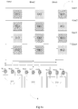
- the display panel comprises pixel groups 1 arranged in a matrix which consist of a plurality of subpixels.
- the respective pixel groups 1 comprise four row and three columns of subpixels, which are red subpixels R, green subpixels G and blue subpixels B; blue subpixels B, red subpixels R and green subpixels G; green subpixels G, blue subpixels B and red subpixels R; blue subpixels B, red subpixels R and green subpixels G, respectively; gate lines Gate connected to the subpixels of respective rows, data lines Data connected to the subpixels of respective columns, and operational amplifiers 2 connected to the respective data lines Data in one-to-one correspondence.
- the above display panel virtually designed can reduce the number of subpixels by a third while achieving the same display effect by means of such particular Rainbow subpixel arrangement manner and corresponding virtual algorithm.
- the operational amplifiers 2 need to output data signals to the subpixels of respective colors connected to the corresponding data line successively according to the scanning order.
- the previous row of the green subpixels G may be red subpixels R and may also be blue subpixels B.
- the grayscale values of R, G, B are all different, the grayscale values outputted by the same operational amplifier are jumping all the time.
- the grayscale value 127 outputted by the operational amplifier to the green subpixels G may result from jumping from 0 of the previous row, and may also result from jumping from 255 of the previous row.
- embodiments of the present disclosure provide a display panel, a driving method and a display apparatus for eliminating the bright and dark horizontal stripes presented on the display panel when displaying a picture of solid color, thereby improving the display effect of the display panel.
- a first aspect of the present disclosure provides a display panel which may comprise: several pixel groups arranged in a matrix which consist of N-row ⁇ M-column subpixels, gate lines connected to subpixels of respective rows, and data lines connected to subpixels of respective columns; wherein N is a positive integer larger than 2, M is a positive integer larger than 1, and in one and the same pixel group, subpixels of the same column comprise subpixels of at least two colors.
- the display panel further comprises a plurality of operational amplifiers corresponding to respective data lines, respective operational amplifiers being connected to corresponding data lines via corresponding switching devices, respectively, and a control unit connected to respective switching devices.
- the number of operational amplifiers corresponding to each data line is equal to that of color types of subpixels connected to the data line, and one operational amplifier corresponds to subpixels of one color.
- respective operational amplifiers are used to output data signals to subpixels of corresponding colors connected to the corresponding data line successively according to a scanning order of the gate lines.
- the control unit is used to, for subpixels of the m-th column of the display panel, control one of the switching devices connected to the data line that is connected to the subpixels of the m-th column to be in conducting state when the gate line of the n-th row is scanned, and the switching device in conducting state is a switching device connected to the operational amplifier for outputting data signals to the subpixels of the n-th row.
- the data lines connected with the subpixels of the same color may correspond to the same operational amplifier that outputs data signals to the subpixels of the same color.
- the number of color types of the subpixels in each column of subpixels may be the same, and the color types may be the same.
- subpixels of a first row may be a subpixel of a first color, a subpixel of a second color and a subpixel of a third color, respectively
- subpixels of a second row may be a subpixel of the third color
- a subpixel of the first color and a subpixel of the second color respectively
- subpixels of a third row may be a subpixel of the second color
- subpixel of the third color and a subpixel of the first color respectively
- subpixels of a fourth row may be a subpixels of the third color, a subpixel of the first color and a subpixel of the second color, respectively.
- the first color, the second color and the third color may be one of red, green and blue, respectively.
- the switching device may be a transmission gate.
- a positive phase control terminal and a negative phase control terminal of the transmission gate are both connected to the control unit, an input terminal of the transmission gate is connected to corresponding operational amplifiers, and an output terminal of the transmission gate is connected to corresponding data lines.
- the switching device may be a switching transistor.
- a gate of the switching transistor is connected to the control unit, a first end of the switching transistor is connected to corresponding operational amplifiers, a second end of the switching transistor is connected to corresponding data lines, and the first end and the second end are one of a source and a drain, respectively.
- the source of a transistor is not distinguished from the drain thereof. Therefore, the first end of the above transistor can indicate both the source and the drain, and the second end can also indicate both the drain and the source, as long as the first end is different from the second end.
- the switching transistor may be an N-type transistor or P-type transistor.
- a second aspect of the present disclosure further provides a method for driving any display panel stated above.
- the method may comprise:
- a third aspect of the present disclosure further provides a display apparatus comprising any display panel provided by embodiments of the present disclosure.
- the data signals are outputted by different operational amplifiers to the subpixels of different colors connected to the same data line, and the data signals are outputted by the same operational amplifier to the subpixels of the same color connected with the same data line, when the above display panel displays one frame of picture of solid color, even if the subpixels of different colors correspond to different grayscale values, since the subpixels of the same color connected to the same data line correspond to the same operational amplifier, that is, the data signals of the subpixels of the same color which have the same grayscale value are always outputted by the same operational amplifier, grayscale jump would not take place. Consequently, the charging amounts for the subpixels of the same color are identical and the brightnesses thereof are also the same upon display, thereby eliminating the bright and dark horizontal stripes presented on the display panel when displaying a picture of solid color and improving the display effect of the display panel.
- a display panel provided by embodiments of the present disclosure comprises, as shown in Fig 2 , several pixel groups 1 arranged in a matrix which consist of N-row ⁇ M-column subpixels 01, gate lines Gate connected to subpixels 01 of respective rows, and data lines Data connected to subpixels 01 of respective columns; wherein N is a positive integer greater than 2, M is a positive integer greater than 1, and in one and the same pixel group 1, the subpixels 01 of the same column comprise subpixels 01 of at least two colors.
- the display panel further comprises a plurality of operational amplifiers (21, 22 and 23 in Fig 2 ) corresponding to respective data lines Data, respective operational amplifiers being connected to corresponding data lines Data via corresponding switching devices 3, and a control unit 4 connected to respective switching devices 3.
- the number of the operational amplifiers corresponding to each data line Data is equal to the number of color types of the subpixels 01 connected to the data line Data, and one operational amplifier (21, 22 or 23) corresponds to subpixels 01 of one color (e.g. in Fig 2 21 corresponds to red subpixels R, 22 corresponds to green subpixels G, and 23 corresponds to blue subpixels B).
- the respective operational amplifiers are used to output data signals to the subpixels 01 of corresponding colors which are connected to the corresponding data line Data successively according to the scanning order of the gate lines Gate.
- the control unit 4 is used to, for the subpixels 01 of the m-th column of the display panel, control one of the switching devices 3 connected to the data line Data that is connected to the subpixels 01 of the m-th column to be in conducting state when the gate line Gate of the n-th row is scanned, and the switching device 3 in conducting state is a switching device 3 connected to the operational amplifiers for outputting data signals to the subpixels 01 of the n-th row.
- the data signals are outputted by different operational amplifiers to the subpixels of different colors connected to the same data line, and the data signals are outputted by the same operational amplifier to the subpixels of the same color connected with the same data line
- the above display panel displays one frame of picture of solid color
- the subpixels of different colors correspond to different grayscale values
- the subpixels of the same color connected to the same data line correspond to the same operational amplifier, that is, the data signals of the subpixels of the same color which have the same grayscale value are always outputted by the same operational amplifier, grayscale jump would not take place. Consequently, the charging amounts for the subpixels of the same color are identical and the brightnesses thereof are also the same upon display, thereby eliminating the bright and dark horizontal stripes presented on the display panel when displaying a picture of solid color and improving the display effect of the display panel.
- the data lines Data connected with the subpixels 01 of the same color correspond to the same operational amplifier which outputs data signals to the subpixels 01 of the same color.
- one column of pixel groups 1 has three columns of subpixels, then it corresponds to three data lines Data, and subpixels 01 of the first column, subpixels 01 of the second column and subpixels 01 of the third column all comprise red subpixels R, green subpixels G and blue subpixels B.
- the three data lines Data are all connected to the same operational amplifier (21 in Fig 3 ) corresponding to the red subpixels R, the same operational amplifier (22 in Fig 3 ) corresponding to the green subpixels G, and the same operational amplifier (23 in Fig 3 ) corresponding to the blue subpixels B.
- the three data lines corresponding to one column of pixel groups are connected to three operational amplifiers (21, 22 and 23 in Fig 3 ), respectively. In this way, the number of amplifiers can be reduced by sharing the amplifiers, thereby reducing the cost.
- each column of subpixels comprises subpixels of three colors, and the types of the three colors in each column of subpixels are the same.
- each data line is connected to the same number of operational amplifiers, and each operational amplifier is connected to each data line corresponding to one and the same pixel group.
- the above display panel provided by embodiments is particular suitable for a display panel in Rainbow arrangement manner.
- the subpixels 01 of the first row are a subpixel 011 of a first color, a subpixel 012 of a second color and a subpixel 013 of a third color, respectively;
- the subpixels 01 of the second row are a subpixel 013 of the third color, a subpixel 011 of the first color and a subpixel 012 of the second color, respectively;
- the subpixels of the third row are a subpixel 012 of the second color, a subpixel 013 of the third color and a subpixel 011 of the first color, respectively;
- the subpixels of the fourth row are a subpixel 013 of the third color, a subpixel 011 of the first color and a subpixel 012 of the second color, respectively.
- the first color, the second color and the third color are one of red, green and blue, respectively. Assuming that the first color is red, the second color can only be green or blue, and the third color can only be blue or green.
- one pixel group is taken as an example, wherein the data lines connected to respective columns of subpixels in one-to-one correspondence are Data 1, Data 2 and Data 3, respectively, the gate lines connected to respective rows of subpixels in one-to-one correspondence are Gate 1, Gate 2, Gate 3 and Gate 4, respectively, the operational amplifier for providing a data signal to the subpixel 011 of the first color is 211, the operational amplifier for providing a data signal to the subpixel 012 of the second color is 212, and the operational amplifier for providing a data signal to the subpixel 013 of the third color is 213.
- the switching device may be a transmission gate, a switching transistor or other electronic switching devices, which are not defined here.
- the switching device may be a transmission gate in the above display panel provided by embodiments of the present disclosure.
- the switching device 3 is a transmission gate (in Fig 4a the three transmission gates connected to the data line Data 1 are TG11, TG12 and TG13, respectively, the three transmission gates connected to the data line Data 2 are TG21, TG22 and TG23, respectively, and the three transmission gates connected to the data line Data 3 are TG31, TG32 and TG33, respectively).
- the positive phase control terminal and the negative phase control terminal of the transmission gate are both connected to the control unit 4, the input terminal thereof is connected to a corresponding operational amplifier 2, and the output terminal thereof is connected to a corresponding data line Data.
- the transmission gate When the signal of the positive phase control terminal is a high level signal, and the signal of the negative phase control terminal is a low level signal, the transmission gate is in conducting state; when the signal of the positive phase control terminal is a low level signal, and the signal of the negative phase control terminal is a high level signal, the transmission gate TG is in cut-off state.
- the switching device 3 is a switching transistor (in Figs 4b and 4c the three switching transistors connected to the data line Data 1 are T11, T12 and T13, respectively, the three switching transistors connected to the data line Data 2 are T21, T22 and T23, respectively, and the three switching transistors connected to the data line Data 3 are T31, T32 and T33, respectively).
- the gate of the switching transistor is connected to the control unit 4, the source thereof is connected to a corresponding operational amplifier 2, and the drain thereof is connected to a corresponding data line Data.
- the source of the switching transistor is not distinguished from the drain thereof. Therefore, in the above arrangement, it is also possible that the drain of the switching transistor is connected to a corresponding operational amplifier 2, and the source thereof is connected to a corresponding data line Data.
- the switching transistor may be an N-type transistor or may also be a P-type transistor.
- the switching transistor when the switching transistor is an N-type transistor and the signal of the gate is a high level signal, the switching transistor is in conducting state; when the signal of the gate is a low level signal, the switching transistor is in cut-off state.
- the switching transistor when the switching transistor is a P-type transistor and the signal of the gate is a low level signal, the switching transistor is in conducting state; when the signal of the gate is a high level signal, the switching transistor is in cut-off state.
- the control unit can send the same control signal to the gates of these switching transistors in conducting state to control these switching transistors to be in conducting state simultaneously or in cut-off state simultaneously.
- the switching transistors T11, T22 and T33 are in conducting state simultaneously, the switching transistors T13, T21 and T32 are in cut-off state simultaneously, and the switching transistors T12, T23 and T31 are in cut-off state simultaneously.
- the switching transistors T13, T21 and T32 are in conducting state simultaneously, the switching transistors T11, T22 and T33 are in cut-off state simultaneously, and the switching transistors T12, T23 and T31 are in cut-off state simultaneously.
- the switching transistors T12, T23 and T31 are in conducting state simultaneously, the switching transistors T13, T21 and T32 are in cut-off state simultaneously, and the switching transistors T11, T22 and T33 are in cut-off state simultaneously.
- the switching transistors T11, T22 and T33 are in conducting state simultaneously, the switching transistors T13, T21 and T32 are in cut-off state simultaneously, and the switching transistors T12, T23 and T31 are in cut-off state simultaneously.
- the switching transistors T11, T22 and T33 are always in conducting state or cut-off state simultaneously, the switching transistors T12, T23 and T31 are always in conducting state or cut-off state simultaneously, and the switching transistors T13, T21 and T32 are always in conducting state or cut-off state simultaneously. Therefore, as shown in Fig 5 , the control unit (not shown in Fig 5 ) can send the same control signal C1 to the switching transistors T11, T22 and T33, send the same control signal C2 to the switching transistors T12, T23 and T31, and send the same control signal C3 to the switching transistors T13, T21 and T32.
- the switching transistors T11, T22 and T33 are in conducting state, and the remaining switching transistors are in cut-off state.
- the operational amplifier 211 provides a data signal to the subpixel 011 of the first color in the first row via the switching transistor T11
- the operational amplifier 212 provides a data signal to the subpixel 012 of the second color in the first row via the switching transistor T22
- the operational amplifier 213 provides a data signal to the subpixel 013 of the third color in the first row via the switching transistor T33.
- the switching transistors T12, T23 and T31 are in conducting state, and the remaining switching transistors are in cut-off state.
- the operational amplifier 211 provides a data signal to the subpixel 011 of the first color in the second row via the switching transistor T12
- the operational amplifier 212 provides a data signal to the subpixel 012 of the second color in the second row via the switching transistor T23
- the operational amplifier 213 provides a data signal to the subpixel 013 of the third color in the second row via the switching transistor T31.
- the switching transistors T13, T21 and T32 are in conducting state, and the remaining switching transistors are in cut-off state.
- the operational amplifier 211 provides a data signal to the subpixel 011 of the first color in the third row via the switching transistor T13
- the operational amplifier 212 provides a data signal to the subpixel 012 of the second color in the third row via the switching transistor T21
- the operational amplifier 213 provides a data signal to the subpixel 013 of the third color in the third row via the switching transistor T32.
- the switching transistors T12, T23 and T31 are in conducting state, and the remaining switching transistors are in cut-off state.
- the operational amplifier 211 provides a data signal to the subpixel 011 of the first color in the fourth row via the switching transistor T12
- the operational amplifier 212 provides a data signal to the subpixel 012 of the second color in the fourth row via the switching transistor T23
- the operational amplifier 213 provides a data signal to the subpixel 013 of the third color in the fourth row via the switching transistor T31.
- embodiments of the present disclosure further provide a method for driving any display panel stated above, comprising:
- embodiments of the present disclosure further provide a display apparatus comprising any of the above display panels provided by embodiments of the present disclosure.
- the display apparatus may be any product or component having display function such as mobile phone, tablet computer, television, display, notebook computer, digital frame, navigator, and so on. Implementation of the display apparatus may refer to the embodiments of the above display panel. Repeated parts are not described here for simplicity.
- the data signals are outputted by different operational amplifiers to the subpixels of different colors connected to the same data line, and the data signals are outputted by the same operational amplifier to the subpixels of the same color connected with the same data line, when the above display panel displays one frame of picture of solid color, even if the subpixels of different colors correspond to different grayscale values, since the subpixels of the same color connected to the same data line correspond to the same operational amplifier, that is, the data signals of the subpixels of the same color which have the same grayscale value are always outputted by the same operational amplifier, grayscale jump would not take place. Consequently, the charging amounts for the subpixels of the same color are identical and the brightnesses thereof are also the same upon display, thereby eliminating the bright and dark horizontal stripes presented on the display panel when displaying a picture of solid color and improving the display effect of the display panel.
Applications Claiming Priority (2)
| Application Number | Priority Date | Filing Date | Title |
|---|---|---|---|
| CN201510202920.6A CN104766564B (zh) | 2015-04-24 | 2015-04-24 | 一种显示面板、其驱动方法及显示装置 |
| PCT/CN2015/089605 WO2016169194A1 (zh) | 2015-04-24 | 2015-09-15 | 一种显示面板、驱动方法及显示装置 |
Publications (3)
| Publication Number | Publication Date |
|---|---|
| EP3288015A1 true EP3288015A1 (de) | 2018-02-28 |
| EP3288015A4 EP3288015A4 (de) | 2018-09-19 |
| EP3288015B1 EP3288015B1 (de) | 2020-05-06 |
Family
ID=53648354
Family Applications (1)
| Application Number | Title | Priority Date | Filing Date |
|---|---|---|---|
| EP15882907.7A Active EP3288015B1 (de) | 2015-04-24 | 2015-09-15 | Anzeigetafel, ansteuerungsverfahren und anzeigevorrichtung |
Country Status (4)
| Country | Link |
|---|---|
| US (1) | US9786211B2 (de) |
| EP (1) | EP3288015B1 (de) |
| CN (1) | CN104766564B (de) |
| WO (1) | WO2016169194A1 (de) |
Cited By (1)
| Publication number | Priority date | Publication date | Assignee | Title |
|---|---|---|---|---|
| CN111986604A (zh) * | 2020-08-12 | 2020-11-24 | 深圳市华星光电半导体显示技术有限公司 | 像素驱动结构以及显示装置 |
Families Citing this family (14)
| Publication number | Priority date | Publication date | Assignee | Title |
|---|---|---|---|---|
| CN104766564B (zh) * | 2015-04-24 | 2017-03-15 | 京东方科技集团股份有限公司 | 一种显示面板、其驱动方法及显示装置 |
| CN104966482B (zh) | 2015-07-27 | 2018-04-20 | 京东方科技集团股份有限公司 | 数据驱动电路及其驱动方法、数据驱动系统和显示装置 |
| CN105609060B (zh) * | 2016-03-10 | 2019-02-12 | 上海天马微电子有限公司 | 背光单元、显示屏以及显示装置 |
| KR20180024987A (ko) * | 2016-08-31 | 2018-03-08 | 엘지디스플레이 주식회사 | 유기 발광 표시 장치 |
| CN106842657A (zh) * | 2017-03-27 | 2017-06-13 | 武汉华星光电技术有限公司 | 一种液晶面板驱动电路及液晶显示装置 |
| US10553173B2 (en) * | 2017-04-17 | 2020-02-04 | A.U. Vista, Inc. | Display with wireless data driving and method for making same |
| CN109785804B (zh) * | 2017-11-13 | 2021-04-09 | 咸阳彩虹光电科技有限公司 | 一种显示方法、显示单元及显示器 |
| KR102525974B1 (ko) * | 2018-06-12 | 2023-04-27 | 삼성디스플레이 주식회사 | 표시 장치 및 이의 구동 방법 |
| CN109545146B (zh) * | 2018-12-13 | 2020-07-03 | 昆山国显光电有限公司 | 一种oled显示面板驱动电路及oled显示面板 |
| CN109671405B (zh) | 2019-01-02 | 2021-02-02 | 京东方科技集团股份有限公司 | 一种阵列基板、显示面板及其驱动方法 |
| CN109920389B (zh) * | 2019-04-29 | 2021-08-31 | 上海天马微电子有限公司 | 一种显示面板、其驱动方法及显示装置 |
| CN110634934A (zh) * | 2019-09-29 | 2019-12-31 | 武汉天马微电子有限公司 | 一种显示面板及显示装置 |
| CN110599942A (zh) * | 2019-09-30 | 2019-12-20 | 京东方科技集团股份有限公司 | 显示面板的驱动方法及装置、显示装置 |
| CN113936619B (zh) * | 2021-10-28 | 2022-08-23 | 深圳市华星光电半导体显示技术有限公司 | 液晶显示面板及其驱动方法、终端 |
Family Cites Families (11)
| Publication number | Priority date | Publication date | Assignee | Title |
|---|---|---|---|---|
| KR100229380B1 (ko) * | 1997-05-17 | 1999-11-01 | 구자홍 | 디지탈방식의 액정표시판넬 구동회로 |
| JP2001343636A (ja) * | 2000-05-31 | 2001-12-14 | Sharp Corp | マトリクス型カラー表示装置 |
| US7764278B2 (en) * | 2005-06-30 | 2010-07-27 | Seiko Epson Corporation | Integrated circuit device and electronic instrument |
| JP4840908B2 (ja) * | 2005-12-07 | 2011-12-21 | ルネサスエレクトロニクス株式会社 | 表示装置駆動回路 |
| KR101423197B1 (ko) * | 2006-12-11 | 2014-07-25 | 삼성디스플레이 주식회사 | 데이터 구동 장치 및 그것을 이용하는 액정 표시 장치 |
| JP2008185644A (ja) * | 2007-01-26 | 2008-08-14 | Nec Electronics Corp | 液晶表示装置及び液晶表示装置の駆動方法 |
| KR100873707B1 (ko) * | 2007-07-27 | 2008-12-12 | 삼성모바일디스플레이주식회사 | 유기전계발광 표시장치 및 그의 구동방법 |
| KR101451589B1 (ko) * | 2012-12-11 | 2014-10-16 | 엘지디스플레이 주식회사 | 영상 표시장치와 그 구동방법 |
| CN104464607B (zh) * | 2013-09-17 | 2017-09-29 | 昆山工研院新型平板显示技术中心有限公司 | 有机发光显示器的像素电路及其驱动方法 |
| CN104200784B (zh) | 2014-07-24 | 2017-07-28 | 京东方科技集团股份有限公司 | 像素驱动电路及其驱动方法、阵列基板、透反式显示装置 |
| CN104766564B (zh) * | 2015-04-24 | 2017-03-15 | 京东方科技集团股份有限公司 | 一种显示面板、其驱动方法及显示装置 |
-
2015
- 2015-04-24 CN CN201510202920.6A patent/CN104766564B/zh active Active
- 2015-09-15 WO PCT/CN2015/089605 patent/WO2016169194A1/zh active Application Filing
- 2015-09-15 US US15/122,632 patent/US9786211B2/en active Active
- 2015-09-15 EP EP15882907.7A patent/EP3288015B1/de active Active
Cited By (2)
| Publication number | Priority date | Publication date | Assignee | Title |
|---|---|---|---|---|
| CN111986604A (zh) * | 2020-08-12 | 2020-11-24 | 深圳市华星光电半导体显示技术有限公司 | 像素驱动结构以及显示装置 |
| CN111986604B (zh) * | 2020-08-12 | 2022-01-25 | 深圳市华星光电半导体显示技术有限公司 | 像素驱动结构以及显示装置 |
Also Published As
| Publication number | Publication date |
|---|---|
| CN104766564A (zh) | 2015-07-08 |
| WO2016169194A1 (zh) | 2016-10-27 |
| EP3288015A4 (de) | 2018-09-19 |
| EP3288015B1 (de) | 2020-05-06 |
| CN104766564B (zh) | 2017-03-15 |
| US20170069243A1 (en) | 2017-03-09 |
| US9786211B2 (en) | 2017-10-10 |
Similar Documents
| Publication | Publication Date | Title |
|---|---|---|
| US9786211B2 (en) | Display panel, driving method and display apparatus | |
| US9892673B2 (en) | Display substrate, display apparatus and driving method thereof | |
| US10049638B2 (en) | Demultiplex type display driving circuit | |
| US9934752B2 (en) | Demultiplex type display driving circuit | |
| US10222665B2 (en) | Array substrate and driving method for the same, display device | |
| US10923054B2 (en) | Array substrate, display panel, display device, and driving methods thereof | |
| US10510315B2 (en) | Display panel, driving method thereof and display device | |
| KR101977514B1 (ko) | Tft 어레이 기판 | |
| US20170053608A1 (en) | Array substrate, display panel and display apparatus containing the same, and method for driving the same | |
| US9761168B2 (en) | Display panel, display method thereof, as well as display device | |
| US10971091B2 (en) | Array substrate, display panel and driving method thereof, and display device | |
| US9099030B2 (en) | Display device | |
| CN113707090B (zh) | 像素驱动电路的驱动方法、显示面板和显示装置 | |
| JP2018501516A (ja) | 液晶パネルの駆動回路及び液晶表示装置 | |
| US10068537B2 (en) | Image processor, display device including the same and method for driving display panel using the same | |
| CN108806586B (zh) | 显示面板、其驱动方法及显示装置 | |
| US9754525B2 (en) | Display panel and driving method thereof and display device | |
| US10223995B2 (en) | Display device having a liquid crystal display panel and an OLED backlight | |
| CN104282260A (zh) | 显示装置、用于显示装置的驱动方法和电子设备 | |
| EP3364402A1 (de) | Pixelstruktur für organische leuchtdiode (oled), ansteuerungsverfahren, ansteuerungsschaltung und anzeigevorrichtung | |
| CN109448642B (zh) | 显示模组及其驱动方法和显示装置 | |
| US9697781B2 (en) | Liquid crystal display device with a plurality of synchronized timing controllers and display driving method thereof | |
| CN115116398A (zh) | 显示面板的驱动方法及显示装置 | |
| US8994632B2 (en) | Liquid crystal display device | |
| KR102306985B1 (ko) | 디스플레이 장치 |
Legal Events
| Date | Code | Title | Description |
|---|---|---|---|
| STAA | Information on the status of an ep patent application or granted ep patent |
Free format text: STATUS: THE INTERNATIONAL PUBLICATION HAS BEEN MADE |
|
| PUAI | Public reference made under article 153(3) epc to a published international application that has entered the european phase |
Free format text: ORIGINAL CODE: 0009012 |
|
| STAA | Information on the status of an ep patent application or granted ep patent |
Free format text: STATUS: REQUEST FOR EXAMINATION WAS MADE |
|
| 17P | Request for examination filed |
Effective date: 20160830 |
|
| AK | Designated contracting states |
Kind code of ref document: A1 Designated state(s): AL AT BE BG CH CY CZ DE DK EE ES FI FR GB GR HR HU IE IS IT LI LT LU LV MC MK MT NL NO PL PT RO RS SE SI SK SM TR |
|
| AX | Request for extension of the european patent |
Extension state: BA ME |
|
| DAV | Request for validation of the european patent (deleted) | ||
| DAX | Request for extension of the european patent (deleted) | ||
| A4 | Supplementary search report drawn up and despatched |
Effective date: 20180817 |
|
| RIC1 | Information provided on ipc code assigned before grant |
Ipc: G09G 3/20 20060101AFI20180810BHEP |
|
| STAA | Information on the status of an ep patent application or granted ep patent |
Free format text: STATUS: EXAMINATION IS IN PROGRESS |
|
| 17Q | First examination report despatched |
Effective date: 20190712 |
|
| GRAP | Despatch of communication of intention to grant a patent |
Free format text: ORIGINAL CODE: EPIDOSNIGR1 |
|
| STAA | Information on the status of an ep patent application or granted ep patent |
Free format text: STATUS: GRANT OF PATENT IS INTENDED |
|
| INTG | Intention to grant announced |
Effective date: 20191220 |
|
| GRAS | Grant fee paid |
Free format text: ORIGINAL CODE: EPIDOSNIGR3 |
|
| GRAA | (expected) grant |
Free format text: ORIGINAL CODE: 0009210 |
|
| STAA | Information on the status of an ep patent application or granted ep patent |
Free format text: STATUS: THE PATENT HAS BEEN GRANTED |
|
| AK | Designated contracting states |
Kind code of ref document: B1 Designated state(s): AL AT BE BG CH CY CZ DE DK EE ES FI FR GB GR HR HU IE IS IT LI LT LU LV MC MK MT NL NO PL PT RO RS SE SI SK SM TR |
|
| REG | Reference to a national code |
Ref country code: GB Ref legal event code: FG4D |
|
| REG | Reference to a national code |
Ref country code: CH Ref legal event code: EP Ref country code: AT Ref legal event code: REF Ref document number: 1268073 Country of ref document: AT Kind code of ref document: T Effective date: 20200515 |
|
| REG | Reference to a national code |
Ref country code: IE Ref legal event code: FG4D |
|
| REG | Reference to a national code |
Ref country code: DE Ref legal event code: R096 Ref document number: 602015052569 Country of ref document: DE |
|
| REG | Reference to a national code |
Ref country code: LT Ref legal event code: MG4D |
|
| REG | Reference to a national code |
Ref country code: NL Ref legal event code: MP Effective date: 20200506 |
|
| PG25 | Lapsed in a contracting state [announced via postgrant information from national office to epo] |
Ref country code: PT Free format text: LAPSE BECAUSE OF FAILURE TO SUBMIT A TRANSLATION OF THE DESCRIPTION OR TO PAY THE FEE WITHIN THE PRESCRIBED TIME-LIMIT Effective date: 20200907 Ref country code: LT Free format text: LAPSE BECAUSE OF FAILURE TO SUBMIT A TRANSLATION OF THE DESCRIPTION OR TO PAY THE FEE WITHIN THE PRESCRIBED TIME-LIMIT Effective date: 20200506 Ref country code: GR Free format text: LAPSE BECAUSE OF FAILURE TO SUBMIT A TRANSLATION OF THE DESCRIPTION OR TO PAY THE FEE WITHIN THE PRESCRIBED TIME-LIMIT Effective date: 20200807 Ref country code: NO Free format text: LAPSE BECAUSE OF FAILURE TO SUBMIT A TRANSLATION OF THE DESCRIPTION OR TO PAY THE FEE WITHIN THE PRESCRIBED TIME-LIMIT Effective date: 20200806 Ref country code: SE Free format text: LAPSE BECAUSE OF FAILURE TO SUBMIT A TRANSLATION OF THE DESCRIPTION OR TO PAY THE FEE WITHIN THE PRESCRIBED TIME-LIMIT Effective date: 20200506 Ref country code: IS Free format text: LAPSE BECAUSE OF FAILURE TO SUBMIT A TRANSLATION OF THE DESCRIPTION OR TO PAY THE FEE WITHIN THE PRESCRIBED TIME-LIMIT Effective date: 20200906 Ref country code: FI Free format text: LAPSE BECAUSE OF FAILURE TO SUBMIT A TRANSLATION OF THE DESCRIPTION OR TO PAY THE FEE WITHIN THE PRESCRIBED TIME-LIMIT Effective date: 20200506 |
|
| PG25 | Lapsed in a contracting state [announced via postgrant information from national office to epo] |
Ref country code: RS Free format text: LAPSE BECAUSE OF FAILURE TO SUBMIT A TRANSLATION OF THE DESCRIPTION OR TO PAY THE FEE WITHIN THE PRESCRIBED TIME-LIMIT Effective date: 20200506 Ref country code: LV Free format text: LAPSE BECAUSE OF FAILURE TO SUBMIT A TRANSLATION OF THE DESCRIPTION OR TO PAY THE FEE WITHIN THE PRESCRIBED TIME-LIMIT Effective date: 20200506 Ref country code: HR Free format text: LAPSE BECAUSE OF FAILURE TO SUBMIT A TRANSLATION OF THE DESCRIPTION OR TO PAY THE FEE WITHIN THE PRESCRIBED TIME-LIMIT Effective date: 20200506 Ref country code: BG Free format text: LAPSE BECAUSE OF FAILURE TO SUBMIT A TRANSLATION OF THE DESCRIPTION OR TO PAY THE FEE WITHIN THE PRESCRIBED TIME-LIMIT Effective date: 20200806 |
|
| REG | Reference to a national code |
Ref country code: AT Ref legal event code: MK05 Ref document number: 1268073 Country of ref document: AT Kind code of ref document: T Effective date: 20200506 |
|
| PG25 | Lapsed in a contracting state [announced via postgrant information from national office to epo] |
Ref country code: AL Free format text: LAPSE BECAUSE OF FAILURE TO SUBMIT A TRANSLATION OF THE DESCRIPTION OR TO PAY THE FEE WITHIN THE PRESCRIBED TIME-LIMIT Effective date: 20200506 Ref country code: NL Free format text: LAPSE BECAUSE OF FAILURE TO SUBMIT A TRANSLATION OF THE DESCRIPTION OR TO PAY THE FEE WITHIN THE PRESCRIBED TIME-LIMIT Effective date: 20200506 |
|
| PG25 | Lapsed in a contracting state [announced via postgrant information from national office to epo] |
Ref country code: EE Free format text: LAPSE BECAUSE OF FAILURE TO SUBMIT A TRANSLATION OF THE DESCRIPTION OR TO PAY THE FEE WITHIN THE PRESCRIBED TIME-LIMIT Effective date: 20200506 Ref country code: SM Free format text: LAPSE BECAUSE OF FAILURE TO SUBMIT A TRANSLATION OF THE DESCRIPTION OR TO PAY THE FEE WITHIN THE PRESCRIBED TIME-LIMIT Effective date: 20200506 Ref country code: AT Free format text: LAPSE BECAUSE OF FAILURE TO SUBMIT A TRANSLATION OF THE DESCRIPTION OR TO PAY THE FEE WITHIN THE PRESCRIBED TIME-LIMIT Effective date: 20200506 Ref country code: RO Free format text: LAPSE BECAUSE OF FAILURE TO SUBMIT A TRANSLATION OF THE DESCRIPTION OR TO PAY THE FEE WITHIN THE PRESCRIBED TIME-LIMIT Effective date: 20200506 Ref country code: ES Free format text: LAPSE BECAUSE OF FAILURE TO SUBMIT A TRANSLATION OF THE DESCRIPTION OR TO PAY THE FEE WITHIN THE PRESCRIBED TIME-LIMIT Effective date: 20200506 Ref country code: CZ Free format text: LAPSE BECAUSE OF FAILURE TO SUBMIT A TRANSLATION OF THE DESCRIPTION OR TO PAY THE FEE WITHIN THE PRESCRIBED TIME-LIMIT Effective date: 20200506 Ref country code: IT Free format text: LAPSE BECAUSE OF FAILURE TO SUBMIT A TRANSLATION OF THE DESCRIPTION OR TO PAY THE FEE WITHIN THE PRESCRIBED TIME-LIMIT Effective date: 20200506 Ref country code: DK Free format text: LAPSE BECAUSE OF FAILURE TO SUBMIT A TRANSLATION OF THE DESCRIPTION OR TO PAY THE FEE WITHIN THE PRESCRIBED TIME-LIMIT Effective date: 20200506 |
|
| REG | Reference to a national code |
Ref country code: DE Ref legal event code: R097 Ref document number: 602015052569 Country of ref document: DE |
|
| PG25 | Lapsed in a contracting state [announced via postgrant information from national office to epo] |
Ref country code: SK Free format text: LAPSE BECAUSE OF FAILURE TO SUBMIT A TRANSLATION OF THE DESCRIPTION OR TO PAY THE FEE WITHIN THE PRESCRIBED TIME-LIMIT Effective date: 20200506 Ref country code: PL Free format text: LAPSE BECAUSE OF FAILURE TO SUBMIT A TRANSLATION OF THE DESCRIPTION OR TO PAY THE FEE WITHIN THE PRESCRIBED TIME-LIMIT Effective date: 20200506 |
|
| PLBE | No opposition filed within time limit |
Free format text: ORIGINAL CODE: 0009261 |
|
| STAA | Information on the status of an ep patent application or granted ep patent |
Free format text: STATUS: NO OPPOSITION FILED WITHIN TIME LIMIT |
|
| 26N | No opposition filed |
Effective date: 20210209 |
|
| REG | Reference to a national code |
Ref country code: CH Ref legal event code: PL |
|
| GBPC | Gb: european patent ceased through non-payment of renewal fee |
Effective date: 20200915 |
|
| PG25 | Lapsed in a contracting state [announced via postgrant information from national office to epo] |
Ref country code: SI Free format text: LAPSE BECAUSE OF FAILURE TO SUBMIT A TRANSLATION OF THE DESCRIPTION OR TO PAY THE FEE WITHIN THE PRESCRIBED TIME-LIMIT Effective date: 20200506 |
|
| REG | Reference to a national code |
Ref country code: BE Ref legal event code: MM Effective date: 20200930 |
|
| PG25 | Lapsed in a contracting state [announced via postgrant information from national office to epo] |
Ref country code: LU Free format text: LAPSE BECAUSE OF NON-PAYMENT OF DUE FEES Effective date: 20200915 |
|
| PG25 | Lapsed in a contracting state [announced via postgrant information from national office to epo] |
Ref country code: FR Free format text: LAPSE BECAUSE OF NON-PAYMENT OF DUE FEES Effective date: 20200930 |
|
| PG25 | Lapsed in a contracting state [announced via postgrant information from national office to epo] |
Ref country code: CH Free format text: LAPSE BECAUSE OF NON-PAYMENT OF DUE FEES Effective date: 20200930 Ref country code: BE Free format text: LAPSE BECAUSE OF NON-PAYMENT OF DUE FEES Effective date: 20200930 Ref country code: LI Free format text: LAPSE BECAUSE OF NON-PAYMENT OF DUE FEES Effective date: 20200930 Ref country code: GB Free format text: LAPSE BECAUSE OF NON-PAYMENT OF DUE FEES Effective date: 20200915 Ref country code: IE Free format text: LAPSE BECAUSE OF NON-PAYMENT OF DUE FEES Effective date: 20200915 |
|
| PG25 | Lapsed in a contracting state [announced via postgrant information from national office to epo] |
Ref country code: TR Free format text: LAPSE BECAUSE OF FAILURE TO SUBMIT A TRANSLATION OF THE DESCRIPTION OR TO PAY THE FEE WITHIN THE PRESCRIBED TIME-LIMIT Effective date: 20200506 Ref country code: MT Free format text: LAPSE BECAUSE OF FAILURE TO SUBMIT A TRANSLATION OF THE DESCRIPTION OR TO PAY THE FEE WITHIN THE PRESCRIBED TIME-LIMIT Effective date: 20200506 Ref country code: CY Free format text: LAPSE BECAUSE OF FAILURE TO SUBMIT A TRANSLATION OF THE DESCRIPTION OR TO PAY THE FEE WITHIN THE PRESCRIBED TIME-LIMIT Effective date: 20200506 |
|
| PG25 | Lapsed in a contracting state [announced via postgrant information from national office to epo] |
Ref country code: MK Free format text: LAPSE BECAUSE OF FAILURE TO SUBMIT A TRANSLATION OF THE DESCRIPTION OR TO PAY THE FEE WITHIN THE PRESCRIBED TIME-LIMIT Effective date: 20200506 Ref country code: MC Free format text: LAPSE BECAUSE OF FAILURE TO SUBMIT A TRANSLATION OF THE DESCRIPTION OR TO PAY THE FEE WITHIN THE PRESCRIBED TIME-LIMIT Effective date: 20200506 |
|
| PGFP | Annual fee paid to national office [announced via postgrant information from national office to epo] |
Ref country code: DE Payment date: 20220920 Year of fee payment: 8 |