EP3285149A1 - Berührungsbildschirm und berührungsempfindliche vorrichtung - Google Patents
Berührungsbildschirm und berührungsempfindliche vorrichtung Download PDFInfo
- Publication number
- EP3285149A1 EP3285149A1 EP15832677.7A EP15832677A EP3285149A1 EP 3285149 A1 EP3285149 A1 EP 3285149A1 EP 15832677 A EP15832677 A EP 15832677A EP 3285149 A1 EP3285149 A1 EP 3285149A1
- Authority
- EP
- European Patent Office
- Prior art keywords
- touch control
- electrode
- touch
- control sensing
- leads
- Prior art date
- Legal status (The legal status is an assumption and is not a legal conclusion. Google has not performed a legal analysis and makes no representation as to the accuracy of the status listed.)
- Withdrawn
Links
Images


Classifications
-
- G—PHYSICS
- G06—COMPUTING OR CALCULATING; COUNTING
- G06F—ELECTRIC DIGITAL DATA PROCESSING
- G06F3/00—Input arrangements for transferring data to be processed into a form capable of being handled by the computer; Output arrangements for transferring data from processing unit to output unit, e.g. interface arrangements
- G06F3/01—Input arrangements or combined input and output arrangements for interaction between user and computer
- G06F3/03—Arrangements for converting the position or the displacement of a member into a coded form
- G06F3/041—Digitisers, e.g. for touch screens or touch pads, characterised by the transducing means
- G06F3/044—Digitisers, e.g. for touch screens or touch pads, characterised by the transducing means by capacitive means
- G06F3/0443—Digitisers, e.g. for touch screens or touch pads, characterised by the transducing means by capacitive means using a single layer of sensing electrodes
-
- G—PHYSICS
- G06—COMPUTING OR CALCULATING; COUNTING
- G06F—ELECTRIC DIGITAL DATA PROCESSING
- G06F3/00—Input arrangements for transferring data to be processed into a form capable of being handled by the computer; Output arrangements for transferring data from processing unit to output unit, e.g. interface arrangements
- G06F3/01—Input arrangements or combined input and output arrangements for interaction between user and computer
- G06F3/03—Arrangements for converting the position or the displacement of a member into a coded form
- G06F3/041—Digitisers, e.g. for touch screens or touch pads, characterised by the transducing means
- G06F3/0416—Control or interface arrangements specially adapted for digitisers
- G06F3/04164—Connections between sensors and controllers, e.g. routing lines between electrodes and connection pads
-
- G—PHYSICS
- G06—COMPUTING OR CALCULATING; COUNTING
- G06F—ELECTRIC DIGITAL DATA PROCESSING
- G06F2203/00—Indexing scheme relating to G06F3/00 - G06F3/048
- G06F2203/041—Indexing scheme relating to G06F3/041 - G06F3/045
- G06F2203/04104—Multi-touch detection in digitiser, i.e. details about the simultaneous detection of a plurality of touching locations, e.g. multiple fingers or pen and finger
Definitions
- the present invention relates to the field of display technologies, in particular to a touch screen and a touch control device.
- Touch screens have become more and more popular owing to their usability, multi-functionality of operation, continuously lowering price, and steadily increasing yield.
- Touch screens can be divided into external touch screens and embedded touch screens.
- An external touch screen may have a panel with a touch function located in front of a display, and a touch surface covers a viewable area of a display area, thereby realizing touch control; while an embedded touch screen has a touch function integrated into a display panel, with or without a protection glass in the outside, and a user can operate by touching the screen with a finger.
- a touch control structure of the touch screen is formed by a substrate and a touch pattern that consists of touch control electrodes.
- the touch control electrodes include touch control driving electrodes and touch control sensing electrodes, and these touch control electrodes are connected to a touch control drive circuit via electrode leads and lead pins.
- a conventional touch control electrode structure as shown in Figs. 1 and 2 , it is usual that multiple touch control driving electrodes Tx1-Tx10 correspond to one touch control sensing electrode Rx1 or that one touch control driving electrode Tx1 corresponds to two touch control sensing electrodes Rx1 and Rx2, thus there are relatively a larger number of touch control driving electrodes, which result in a larger number of leads and pins.
- a touch screen display of about 5 inches has 200-300 pins, and a screen of 7 inches even has more than 400 pins.
- more touch control driving electrode leads and more lead pins are needed for connecting them to the touch control drive circuit, which increases the difficulty of technology to some extent.
- too many pins will increase the product cost, cause a reduction in the yield of binding between the touch control electrode leads and the touch control drive circuit, and may easily cause such problems as bad curing after the joint.
- An object of the present invention is to provide a touch screen and a touch control device that can solve the above-mentioned problems in the prior art.
- the invention improves the conventional touch control electrode structure of the touch screen by changing a condition that one touch control sensing electrode corresponds to multiple touch control driving electrode in the conventional structure into a condition that one touch control driving electrode corresponds to multiple (e.g. five or more) touch sensing electrodes, thus significantly reducing the number of touch control driving electrodes, as a result, a total number of electrode leads and pins is reduced and the touch control precision is significantly improved.
- the present invention provides a touch screen, which comprises a plurality of touch control electrode units and touch control electrode leads, each of the touch control electrode units comprises one touch control driving electrode and M touch control sensing electrodes, and the touch control electrode leads comprise multiple touch control driving electrode leads and M touch control sensing electrode leads, each touch control driving electrode lead being correspondingly connected to each touch control driving electrode, and each of the M touch control sensing electrode leads being connected to one of the M touch control sensing electrodes in each of the touch control electrode units, wherein M is a positive integer greater than or equal to 5.
- the present invention also provides a touch control device, comprising the above-mentioned touch screen according to the present invention.
- the touch control device may include, but is not limited to, any product or component having a display function, such as liquid crystal panel, electronic paper, OLED panel, liquid crystal television, liquid crystal display, digital photo frame, cell phone, tablet computer, etc.
- the touch screen and touch control device of the present invention have the following advantageous effects: (1) significantly reducing the numbers of touch control driving electrodes and electrode leads while keeping the touch control precision unchanged; (2) significantly increasing the touch control precision while keeping the numbers of touch control driving electrodes and electrode leads unchanged.
- Fig. 1 is a schematic drawing of a first touch control electrode structure of a touch screen according to the prior art.
- such touch control electrode structure has a group of (ten) touch control driving electrodes Tx1-Tx10 corresponding to one touch control sensing electrode Rx1, thus forming a touch control electrode unit (only one touch control electrode unit is shown in the figure), wherein each touch control driving electrode is individually connected via a single one touch control driving electrode lead, namely, 10 touch control driving electrodes Tx1-Tx10 are individually connected via 10 touch control driving electrode leads 101-110, respectively, while the touch control sensing electrode Rx1 in each touch control electrode unit is connected via one touch control sensing electrode lead 201.
- the touch control driving electrode leads 101-110 and the touch control sensing electrode lead 201 are respectively connected to a touch control drive circuit (not shown) via lead pins (not shown).
- the correspondence between a group of touch control driving electrodes and one touch control sensing electrode means that each of the plurality of touch control driving electrodes in the group corresponds to one touch control sensing electrode so as to form touch control detection areas which have the same number as the touch control driving electrodes, and the touch control drive circuit determines a touch control position by detecting a capacitance change therein.
- the touch control electrodes as shown in Fig. 1 form 10 touch control detection areas.
- the first touch control electrode structure of the prior art as shown in Fig.
- the touch control driving electrodes Tx1-Tx10 need 10 touch control driving electrode leads 101-110 and 10 lead pins, and the touch control sensing electrode Rx1 needs one touch control sensing electrode lead 201 and one lead pin, so they together need 11 leads and 11 pins.
- Fig. 2 is a schematic drawing of a second touch control electrode structure of a touch screen according to the prior art.
- the touch control electrode structure shown in Fig. 2 has one touch control driving electrode corresponding to a group of (two) touch control sensing electrodes Rx1 and Rx2, thus forming a touch control electrode unit, wherein each touch control driving electrode is individually connected via a single one touch control driving electrode lead, namely, 5 touch control driving electrodes Tx1-Tx5 are individually connected via 5 touch control driving electrode leads 101-105, respectively, while the touch control sensing electrodes having the same positional sequence in each touch control electrode unit are connected in series via one and the same touch control sensing electrode lead, that is, as shown in Fig.
- a first touch control sensing electrode Rx1 and a second touch control sensing electrode Rx2 of each touch control electrode unit are connected in series by touch control sensing electrode leads 201 and 202 respectively.
- the correspondence between one touch control driving electrode and a group of touch control sensing electrodes means that one touch control driving electrode corresponds to multiple touch control sensing electrodes in the group so as to form multiple touch control detection areas, wherein a number of the touch control detection areas equals to the number of the touch control sensing electrodes.
- the touch control electrode structure as shown in Fig. 2 includes 5 touch control electrode units, thus forming 10 touch control detection areas.
- the second touch control electrode structure of the prior art as shown in Fig.
- the touch control driving electrodes Tx1-Tx5 need 5 touch control driving electrode leads 101-105 and 5 lead pins
- the touch control sensing electrodes Rx1-Rx2 need only two touch control sensing electrode leads 201-202 and two lead pins, so they together need 7 leads and 7 pins.
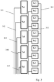
- Fig. 3 is a schematic drawing of a touch control electrode structure of a touch screen according to an embodiment of the present invention.
- the touch screen according to an embodiment of the present invention comprises a plurality of touch control electrode units and a plurality of touch control electrode leads, each touch control electrode unit comprising one touch control driving electrode and M touch control sensing electrodes, wherein M is a positive integer greater than or equal to 5.
- each touch control electrode unit comprises one touch control driving electrode Tx1 or Tx2 and 5 (i.e.
- touch control sensing electrodes Rx1-Rx5 which are the first to fifth touch control sensing electrodes Rx1-Rx5 according to the positional sequence, wherein the touch control driving electrode Tx1 (or Tx2) in different touch control electrode units is individually connected via a single one touch control driving electrode lead 101 (or 102), while the touch control sensing electrodes Rx1-Rx5 having the same positional sequence in each of the touch control electrode units are connected in series via one and the same touch control sensing electrode lead.
- the touch control driving electrode Tx1 (or Tx2) in different touch control electrode units is individually connected via a single one touch control driving electrode lead 101 (or 102)
- the touch control sensing electrodes Rx1-Rx5 having the same positional sequence in each of the touch control electrode units are connected in series via one and the same touch control sensing electrode lead.
- the touch control driving electrodes Tx1 and Tx2 in two different touch control electrode units are individually connected by two different touch control driving electrode leads 101 and 102, respectively, while the first to fifth touch control sensing electrodes Rx1-Rx5 having the same positional sequence in each of the touch control electrode units are connected in series via touch control sensing electrode leads 201-205.
- Such a way of connecting the touch control sensing electrodes according to the positional sequence can realize good touch control sensitivity in each touch control detection area.
- each touch control electrode unit Preferably, in each touch control electrode unit, one touch control driving electrode is arranged opposite M touch control sensing electrodes arranged side by side, so that at least a part of each of the M touch control sensing electrodes corresponds to a part of the touch control driving electrode so as to form a touch control detection area.
- each touch control electrode unit can form M touch control detection areas, and the touch control drive circuit determines the touch control position by detecting a capacitance change therein.
- the touch control electrode structure according to the present invention as shown in Fig. 3 has two touch control electrode units altogether, each including 5 touch control sensing electrodes and hence 5 touch control detection areas, thus the touch control electrode structure shown in Fig. 3 has 10 touch control detection areas altogether.
- the touch control sensing electrode lead may be arranged in other manner, for example, in each of the touch control electrode units, touch control sensing electrodes connected via the same touch control sensing electrode lead are not limited to having the same sequence of arrangement.
- each touch control driving electrode lead is correspondingly connected to each touch control driving electrode
- each of the plurality of touch control sensing electrode leads is connected to one of the plurality of touch control sensing electrodes in each of the touch control electrode units.
- the touch screen as shown in Fig. 3 may further comprise a touch control drive circuit (not shown), which is connected to the touch control electrode via a touch control electrode lead. Further, the touch screen may further comprise a lead pin (not shown), via which the touch control electrode lead is connected to the touch control drive circuit.
- the touch control driving electrode needs two touch control driving electrode leads 101-102 and two lead pins, while the touch control sensing electrode needs five touch control sensing electrode leads 201-205 and five lead pins, so 7 leads and 7 pins are needed altogether, which are the same as the those needed in the second touch control electrode structure of the prior art as shown in Fig. 2 , and are less than those needed in the first touch control electrode structure of the prior art as shown in Fig. 1 .
- Figs. 1-3 only show the case of one column of the touch control electrode structures, and each column of touch control electrode structures includes 10 rows of touch control driving electrodes or touch control sensing electrodes, namely, it includes 10 touch control detection areas.
- a touch screen may comprise multiple columns of such structures, each column having more rows of touch control driving electrodes or touch control sensing electrodes, namely, there are more touch control detection areas.
- each column has 20 rows (i.e. 20 touch control detection areas), and in each column, the number of pins needed by the first touch control electrode structure of the prior art as shown in Fig.
- the number of pins needed by the touch control electrode structure of Fig. 1 equals to the number of touch control driving electrodes or the number of touch control detection areas in each touch control electrode unit plus the number of the touch control sensing electrodes.
- each column of touch control electrode structure has m touch control detection areas (or rows)
- the touch control electrode structure of Fig. 1 needs m+1 pins
- the touch control electrode structure of Fig. 2 needs m/2+2 pins
- the touch control electrode structure of Fig. 3 needs m/5+5 pins.
- the larger the m the more significant the reduction of the pins in the touch control electrode structure according to the present invention as shown in Fig. 3 .
- the touch control electrode structure of the present invention can effectively reduce the number of pins by 40%-50%.
- the numbers of leads and pins required by the touch control electrode structure according to the present invention are significantly reduced, thereby simplifying the manufacturing process.
- the touch control electrode structure according to the present invention can obviously form more touch control detection areas, thus significantly increasing touch control precision.
- the lead pins can be connected to the touch control drive circuit through a flexible printed circuit board.
- the area of the flexible printed circuit board connected thereto is reduced, thus reducing production cost and technology difficulty; meanwhile, a yield of binding between the lead pins and the flexible printed circuit board can be increased and a yield of UV adhesive curing during surface joining can be increased.
- an electrode material in the touch control electrode unit may include ITO or IGZO.
- a material of the touch control electrode lead may include a metal or ITO.
- a touch control device which comprises the above-mentioned touch screen according to the present invention.
- the touch control device may further comprise a display module.
- the touch control device may include, but is not limited to, any product or component having a display function, such as liquid crystal panel, electronic paper, OLED panel, liquid crystal television, liquid crystal display, digital photo frame, cell phone, tablet computer, etc.
Landscapes
- Engineering & Computer Science (AREA)
- General Engineering & Computer Science (AREA)
- Theoretical Computer Science (AREA)
- Human Computer Interaction (AREA)
- Physics & Mathematics (AREA)
- General Physics & Mathematics (AREA)
- Computer Networks & Wireless Communication (AREA)
- Position Input By Displaying (AREA)
Applications Claiming Priority (2)
| Application Number | Priority Date | Filing Date | Title |
|---|---|---|---|
| CN201510176473.1A CN104765499A (zh) | 2015-04-15 | 2015-04-15 | 触摸屏及触控装置 |
| PCT/CN2015/087233 WO2016165251A1 (zh) | 2015-04-15 | 2015-08-17 | 触摸屏及触控装置 |
Publications (2)
| Publication Number | Publication Date |
|---|---|
| EP3285149A1 true EP3285149A1 (de) | 2018-02-21 |
| EP3285149A4 EP3285149A4 (de) | 2019-02-06 |
Family
ID=53647374
Family Applications (1)
| Application Number | Title | Priority Date | Filing Date |
|---|---|---|---|
| EP15832677.7A Withdrawn EP3285149A4 (de) | 2015-04-15 | 2015-08-17 | Berührungsbildschirm und berührungsempfindliche vorrichtung |
Country Status (4)
| Country | Link |
|---|---|
| US (1) | US20170060318A1 (de) |
| EP (1) | EP3285149A4 (de) |
| CN (1) | CN104765499A (de) |
| WO (1) | WO2016165251A1 (de) |
Families Citing this family (15)
| Publication number | Priority date | Publication date | Assignee | Title |
|---|---|---|---|---|
| US8633915B2 (en) | 2007-10-04 | 2014-01-21 | Apple Inc. | Single-layer touch-sensitive display |
| US20090174676A1 (en) | 2008-01-04 | 2009-07-09 | Apple Inc. | Motion component dominance factors for motion locking of touch sensor data |
| CN107077260B (zh) | 2014-09-22 | 2020-05-12 | 苹果公司 | 触摸控制器和用于触摸传感器面板的方法 |
| CN104765499A (zh) * | 2015-04-15 | 2015-07-08 | 合肥京东方光电科技有限公司 | 触摸屏及触控装置 |
| US10534481B2 (en) * | 2015-09-30 | 2020-01-14 | Apple Inc. | High aspect ratio capacitive sensor panel |
| CN105183262B (zh) * | 2015-10-13 | 2019-02-26 | 昆山龙腾光电有限公司 | 一种电容式触控面板 |
| JP6630433B2 (ja) * | 2016-05-12 | 2020-01-15 | アルプスアルパイン株式会社 | 入力装置 |
| CN108509092B (zh) * | 2017-02-27 | 2021-03-12 | 奕力科技(开曼)股份有限公司 | 双层互容式触控面板 |
| US10386965B2 (en) | 2017-04-20 | 2019-08-20 | Apple Inc. | Finger tracking in wet environment |
| CN110134293B (zh) * | 2018-02-09 | 2022-05-10 | 奕力科技股份有限公司 | 互容式触控面板 |
| CN109933244B (zh) * | 2019-05-17 | 2020-07-03 | 深圳市德明利技术股份有限公司 | 一种用于大尺寸触摸屏的触摸屏传感器及触摸识别方法 |
| CN110740035B (zh) | 2019-10-21 | 2021-08-31 | 浙江正泰仪器仪表有限责任公司 | 一种智能表具加密系统以及加密方法 |
| CN111007956A (zh) * | 2019-11-12 | 2020-04-14 | 深圳市华星光电半导体显示技术有限公司 | 显示装置 |
| US11662867B1 (en) | 2020-05-30 | 2023-05-30 | Apple Inc. | Hover detection on a touch sensor panel |
| CN112631460B (zh) * | 2020-12-29 | 2025-07-25 | 北京奕斯伟计算技术股份有限公司 | 触控基板、触控显示面板和触控显示装置 |
Family Cites Families (24)
| Publication number | Priority date | Publication date | Assignee | Title |
|---|---|---|---|---|
| US8576193B2 (en) * | 2008-04-25 | 2013-11-05 | Apple Inc. | Brick layout and stackup for a touch screen |
| US8319747B2 (en) * | 2008-12-11 | 2012-11-27 | Apple Inc. | Single layer touch panel with segmented drive and sense electrodes |
| US9495042B2 (en) * | 2009-04-14 | 2016-11-15 | Atmel Corporation | Two-dimensional position sensor |
| KR101189996B1 (ko) * | 2010-04-19 | 2012-10-12 | (주)멜파스 | 멀티터치 감지를 위한 단일층의 접촉 감지 패널 및 접촉 감지 장치 |
| US20130081869A1 (en) * | 2011-09-30 | 2013-04-04 | Jae Hong Kim | Touch sensing apparatus and method of manufacturing the same |
| US20130100041A1 (en) * | 2011-10-21 | 2013-04-25 | Touch Turns Llc | System for a single-layer sensor having reduced number of interconnect pads for the interconnect periphery of the sensor panel |
| US9182861B2 (en) * | 2012-01-12 | 2015-11-10 | Synaptics Incoporated | Single layer capacitive imaging sensors |
| KR101446722B1 (ko) * | 2012-05-16 | 2014-10-07 | 주식회사 동부하이텍 | 터치 스크린 패널 |
| TW201403767A (zh) * | 2012-07-10 | 2014-01-16 | Wintek Corp | 觸控面板 |
| TW201413514A (zh) * | 2012-09-24 | 2014-04-01 | Wintek Corp | 觸控面板 |
| US9292138B2 (en) * | 2013-02-08 | 2016-03-22 | Parade Technologies, Ltd. | Single layer sensor pattern |
| US20140267137A1 (en) * | 2013-03-14 | 2014-09-18 | Synaptics Incorporated | Proximity sensing using driven ground plane |
| CN203324954U (zh) * | 2013-05-21 | 2013-12-04 | 敦泰科技有限公司 | 一种触摸屏设备及其触摸屏体 |
| CN103246422B (zh) * | 2013-05-21 | 2016-10-26 | 敦泰科技有限公司 | 一种触摸屏设备及其触摸屏体 |
| KR102081606B1 (ko) * | 2013-09-04 | 2020-02-26 | 엘지디스플레이 주식회사 | 터치 ic 및 이를 이용한 터치 스크린 일체형 표시장치 |
| US9081457B2 (en) * | 2013-10-30 | 2015-07-14 | Synaptics Incorporated | Single-layer muti-touch capacitive imaging sensor |
| CN103941936A (zh) * | 2013-11-14 | 2014-07-23 | 上海天马微电子有限公司 | 一种触控结构、触摸屏和触摸显示装置 |
| KR102175699B1 (ko) * | 2013-12-20 | 2020-11-06 | 엘지이노텍 주식회사 | 터치패널 |
| CN103970355B (zh) * | 2014-04-30 | 2017-10-27 | 上海天马微电子有限公司 | 一种触摸面板及触摸装置 |
| CN104035624B (zh) * | 2014-06-30 | 2017-08-08 | 上海天马微电子有限公司 | 触控层、触控面板、触控装置、显示面板和显示装置 |
| US9658726B2 (en) * | 2014-07-10 | 2017-05-23 | Cypress Semiconductor Corporation | Single layer sensor pattern |
| TWI546721B (zh) * | 2014-07-25 | 2016-08-21 | 聯詠科技股份有限公司 | 觸控面板及其電極配置方法 |
| CN104375725B (zh) * | 2014-11-07 | 2021-01-01 | 敦泰科技有限公司 | 单层互电容触摸屏、触摸屏装置、及设备 |
| CN104765499A (zh) * | 2015-04-15 | 2015-07-08 | 合肥京东方光电科技有限公司 | 触摸屏及触控装置 |
-
2015
- 2015-04-15 CN CN201510176473.1A patent/CN104765499A/zh active Pending
- 2015-08-17 US US14/912,917 patent/US20170060318A1/en not_active Abandoned
- 2015-08-17 EP EP15832677.7A patent/EP3285149A4/de not_active Withdrawn
- 2015-08-17 WO PCT/CN2015/087233 patent/WO2016165251A1/zh not_active Ceased
Also Published As
| Publication number | Publication date |
|---|---|
| US20170060318A1 (en) | 2017-03-02 |
| EP3285149A4 (de) | 2019-02-06 |
| WO2016165251A1 (zh) | 2016-10-20 |
| CN104765499A (zh) | 2015-07-08 |
Similar Documents
| Publication | Publication Date | Title |
|---|---|---|
| EP3285149A1 (de) | Berührungsbildschirm und berührungsempfindliche vorrichtung | |
| EP3153956B1 (de) | Kapazitive berührungsstruktur, eingebetteter berührungsbildschirm, anzeigevorrichtung und abtastverfahren dafür | |
| US10088968B2 (en) | Touch panel and display device | |
| US20170192582A1 (en) | Touch-control display device | |
| US20150212643A1 (en) | Touch sensing controller, touch sensing device and touch sensing system including the same | |
| CN106249977B (zh) | 一种触控显示面板及电子设备 | |
| US10216344B2 (en) | In-cell touch panel, method for driving the same, and display device | |
| EP3151097A1 (de) | Zellintegrierter berührungsbildschirm und anzeigevorrichtung | |
| US20160183382A1 (en) | Capacitive image sensor with selectable function electrodes | |
| JP6754736B2 (ja) | タッチディスプレイ装置 | |
| CN106648191B (zh) | 一种触控基板、显示装置及其驱动方法 | |
| US20150324033A1 (en) | Touch sensing device, display device including the same, and method of sensing touch | |
| CN204808294U (zh) | 显示面板及显示装置 | |
| US10572092B2 (en) | Method for acquiring data from resistive film touch panel and resistive film touch panel device | |
| EP3293615A1 (de) | Zellintegrierter berührungsbildschirm und anzeigevorrichtung | |
| US20160209951A1 (en) | Touch substrate, its manufacturing method and display device | |
| KR20160053919A (ko) | 센서 장치, 입력 장치 및 전자 기기 | |
| CN102799332A (zh) | 一种嵌入式单层电容触摸屏 | |
| CN104978069A (zh) | 触控装置 | |
| US10884567B2 (en) | Circuit and method for driving touch substrate, touch device and operating method of the same | |
| WO2018145435A1 (en) | Touch substrate, touch panel and method of fabricating a touch panel | |
| CN113010042B (zh) | 一种触控显示面板 | |
| CN109074197B (zh) | 检测触摸压力的触摸输入装置 | |
| US20210157430A1 (en) | Touch display panel and touch display device | |
| US20170235389A1 (en) | Touch Panel and Display Device |
Legal Events
| Date | Code | Title | Description |
|---|---|---|---|
| PUAI | Public reference made under article 153(3) epc to a published international application that has entered the european phase |
Free format text: ORIGINAL CODE: 0009012 |
|
| 17P | Request for examination filed |
Effective date: 20160219 |
|
| AK | Designated contracting states |
Kind code of ref document: A1 Designated state(s): AL AT BE BG CH CY CZ DE DK EE ES FI FR GB GR HR HU IE IS IT LI LT LU LV MC MK MT NL NO PL PT RO RS SE SI SK SM TR |
|
| AX | Request for extension of the european patent |
Extension state: BA ME |
|
| DAV | Request for validation of the european patent (deleted) | ||
| DAX | Request for extension of the european patent (deleted) | ||
| RIC1 | Information provided on ipc code assigned before grant |
Ipc: G06F 3/041 20060101AFI20181221BHEP |
|
| A4 | Supplementary search report drawn up and despatched |
Effective date: 20190109 |
|
| STAA | Information on the status of an ep patent application or granted ep patent |
Free format text: STATUS: THE APPLICATION IS DEEMED TO BE WITHDRAWN |
|
| 18D | Application deemed to be withdrawn |
Effective date: 20190806 |