EP3282486A1 - Semiconductor structure and fabrication method thereof - Google Patents
Semiconductor structure and fabrication method thereof Download PDFInfo
- Publication number
- EP3282486A1 EP3282486A1 EP17185879.8A EP17185879A EP3282486A1 EP 3282486 A1 EP3282486 A1 EP 3282486A1 EP 17185879 A EP17185879 A EP 17185879A EP 3282486 A1 EP3282486 A1 EP 3282486A1
- Authority
- EP
- European Patent Office
- Prior art keywords
- dielectric layer
- layer
- ion implantation
- top surface
- dummy gate
- Prior art date
- Legal status (The legal status is an assumption and is not a legal conclusion. Google has not performed a legal analysis and makes no representation as to the accuracy of the status listed.)
- Withdrawn
Links
Images



Classifications
-
- H—ELECTRICITY
- H10—SEMICONDUCTOR DEVICES; ELECTRIC SOLID-STATE DEVICES NOT OTHERWISE PROVIDED FOR
- H10D—INORGANIC ELECTRIC SEMICONDUCTOR DEVICES
- H10D30/00—Field-effect transistors [FET]
- H10D30/01—Manufacture or treatment
- H10D30/021—Manufacture or treatment of FETs having insulated gates [IGFET]
- H10D30/024—Manufacture or treatment of FETs having insulated gates [IGFET] of fin field-effect transistors [FinFET]
-
- H—ELECTRICITY
- H10—SEMICONDUCTOR DEVICES; ELECTRIC SOLID-STATE DEVICES NOT OTHERWISE PROVIDED FOR
- H10D—INORGANIC ELECTRIC SEMICONDUCTOR DEVICES
- H10D30/00—Field-effect transistors [FET]
- H10D30/60—Insulated-gate field-effect transistors [IGFET]
- H10D30/62—Fin field-effect transistors [FinFET]
- H10D30/6219—Fin field-effect transistors [FinFET] characterised by the source or drain electrodes
-
- H—ELECTRICITY
- H10—SEMICONDUCTOR DEVICES; ELECTRIC SOLID-STATE DEVICES NOT OTHERWISE PROVIDED FOR
- H10D—INORGANIC ELECTRIC SEMICONDUCTOR DEVICES
- H10D62/00—Semiconductor bodies, or regions thereof, of devices having potential barriers
- H10D62/10—Shapes, relative sizes or dispositions of the regions of the semiconductor bodies; Shapes of the semiconductor bodies
- H10D62/113—Isolations within a component, i.e. internal isolations
- H10D62/115—Dielectric isolations, e.g. air gaps
-
- H—ELECTRICITY
- H10—SEMICONDUCTOR DEVICES; ELECTRIC SOLID-STATE DEVICES NOT OTHERWISE PROVIDED FOR
- H10D—INORGANIC ELECTRIC SEMICONDUCTOR DEVICES
- H10D64/00—Electrodes of devices having potential barriers
- H10D64/01—Manufacture or treatment
- H10D64/017—Manufacture or treatment using dummy gates in processes wherein at least parts of the final gates are self-aligned to the dummy gates, i.e. replacement gate processes
-
- H—ELECTRICITY
- H10—SEMICONDUCTOR DEVICES; ELECTRIC SOLID-STATE DEVICES NOT OTHERWISE PROVIDED FOR
- H10D—INORGANIC ELECTRIC SEMICONDUCTOR DEVICES
- H10D64/00—Electrodes of devices having potential barriers
- H10D64/20—Electrodes characterised by their shapes, relative sizes or dispositions
- H10D64/27—Electrodes not carrying the current to be rectified, amplified, oscillated or switched, e.g. gates
- H10D64/311—Gate electrodes for field-effect devices
- H10D64/411—Gate electrodes for field-effect devices for FETs
- H10D64/511—Gate electrodes for field-effect devices for FETs for IGFETs
- H10D64/512—Disposition of the gate electrodes, e.g. buried gates
- H10D64/513—Disposition of the gate electrodes, e.g. buried gates within recesses in the substrate, e.g. trench gates, groove gates or buried gates
-
- H—ELECTRICITY
- H10—SEMICONDUCTOR DEVICES; ELECTRIC SOLID-STATE DEVICES NOT OTHERWISE PROVIDED FOR
- H10D—INORGANIC ELECTRIC SEMICONDUCTOR DEVICES
- H10D84/00—Integrated devices formed in or on semiconductor substrates that comprise only semiconducting layers, e.g. on Si wafers or on GaAs-on-Si wafers
- H10D84/01—Manufacture or treatment
- H10D84/0123—Integrating together multiple components covered by H10D12/00 or H10D30/00, e.g. integrating multiple IGBTs
- H10D84/0126—Integrating together multiple components covered by H10D12/00 or H10D30/00, e.g. integrating multiple IGBTs the components including insulated gates, e.g. IGFETs
- H10D84/0151—Manufacturing their isolation regions
-
- H—ELECTRICITY
- H10—SEMICONDUCTOR DEVICES; ELECTRIC SOLID-STATE DEVICES NOT OTHERWISE PROVIDED FOR
- H10D—INORGANIC ELECTRIC SEMICONDUCTOR DEVICES
- H10D84/00—Integrated devices formed in or on semiconductor substrates that comprise only semiconducting layers, e.g. on Si wafers or on GaAs-on-Si wafers
- H10D84/01—Manufacture or treatment
- H10D84/02—Manufacture or treatment characterised by using material-based technologies
- H10D84/03—Manufacture or treatment characterised by using material-based technologies using Group IV technology, e.g. silicon technology or silicon-carbide [SiC] technology
- H10D84/038—Manufacture or treatment characterised by using material-based technologies using Group IV technology, e.g. silicon technology or silicon-carbide [SiC] technology using silicon technology, e.g. SiGe
-
- H—ELECTRICITY
- H10—SEMICONDUCTOR DEVICES; ELECTRIC SOLID-STATE DEVICES NOT OTHERWISE PROVIDED FOR
- H10P—GENERIC PROCESSES OR APPARATUS FOR THE MANUFACTURE OR TREATMENT OF DEVICES COVERED BY CLASS H10
- H10P30/00—Ion implantation into wafers, substrates or parts of devices
- H10P30/20—Ion implantation into wafers, substrates or parts of devices into semiconductor materials, e.g. for doping
- H10P30/202—Ion implantation into wafers, substrates or parts of devices into semiconductor materials, e.g. for doping characterised by the semiconductor materials
- H10P30/204—Ion implantation into wafers, substrates or parts of devices into semiconductor materials, e.g. for doping characterised by the semiconductor materials into Group IV semiconductors
-
- H—ELECTRICITY
- H10—SEMICONDUCTOR DEVICES; ELECTRIC SOLID-STATE DEVICES NOT OTHERWISE PROVIDED FOR
- H10P—GENERIC PROCESSES OR APPARATUS FOR THE MANUFACTURE OR TREATMENT OF DEVICES COVERED BY CLASS H10
- H10P30/00—Ion implantation into wafers, substrates or parts of devices
- H10P30/20—Ion implantation into wafers, substrates or parts of devices into semiconductor materials, e.g. for doping
- H10P30/21—Ion implantation into wafers, substrates or parts of devices into semiconductor materials, e.g. for doping of electrically active species
-
- H—ELECTRICITY
- H10—SEMICONDUCTOR DEVICES; ELECTRIC SOLID-STATE DEVICES NOT OTHERWISE PROVIDED FOR
- H10P—GENERIC PROCESSES OR APPARATUS FOR THE MANUFACTURE OR TREATMENT OF DEVICES COVERED BY CLASS H10
- H10P52/00—Grinding, lapping or polishing of wafers, substrates or parts of devices
- H10P52/40—Chemomechanical polishing [CMP]
- H10P52/402—Chemomechanical polishing [CMP] of semiconductor materials
-
- H—ELECTRICITY
- H10—SEMICONDUCTOR DEVICES; ELECTRIC SOLID-STATE DEVICES NOT OTHERWISE PROVIDED FOR
- H10W—GENERIC PACKAGES, INTERCONNECTIONS, CONNECTORS OR OTHER CONSTRUCTIONAL DETAILS OF DEVICES COVERED BY CLASS H10
- H10W10/00—Isolation regions in semiconductor bodies between components of integrated devices
- H10W10/01—Manufacture or treatment
- H10W10/011—Manufacture or treatment of isolation regions comprising dielectric materials
- H10W10/014—Manufacture or treatment of isolation regions comprising dielectric materials using trench refilling with dielectric materials, e.g. shallow trench isolations
-
- H—ELECTRICITY
- H10—SEMICONDUCTOR DEVICES; ELECTRIC SOLID-STATE DEVICES NOT OTHERWISE PROVIDED FOR
- H10W—GENERIC PACKAGES, INTERCONNECTIONS, CONNECTORS OR OTHER CONSTRUCTIONAL DETAILS OF DEVICES COVERED BY CLASS H10
- H10W10/00—Isolation regions in semiconductor bodies between components of integrated devices
- H10W10/10—Isolation regions comprising dielectric materials
- H10W10/17—Isolation regions comprising dielectric materials formed using trench refilling with dielectric materials, e.g. shallow trench isolations
-
- H—ELECTRICITY
- H10—SEMICONDUCTOR DEVICES; ELECTRIC SOLID-STATE DEVICES NOT OTHERWISE PROVIDED FOR
- H10W—GENERIC PACKAGES, INTERCONNECTIONS, CONNECTORS OR OTHER CONSTRUCTIONAL DETAILS OF DEVICES COVERED BY CLASS H10
- H10W20/00—Interconnections in chips, wafers or substrates
- H10W20/01—Manufacture or treatment
- H10W20/071—Manufacture or treatment of dielectric parts thereof
- H10W20/074—Manufacture or treatment of dielectric parts thereof of dielectric parts comprising thin functional dielectric layers, e.g. dielectric etch-stop, barrier, capping or liner layers
-
- H—ELECTRICITY
- H10—SEMICONDUCTOR DEVICES; ELECTRIC SOLID-STATE DEVICES NOT OTHERWISE PROVIDED FOR
- H10D—INORGANIC ELECTRIC SEMICONDUCTOR DEVICES
- H10D84/00—Integrated devices formed in or on semiconductor substrates that comprise only semiconducting layers, e.g. on Si wafers or on GaAs-on-Si wafers
- H10D84/01—Manufacture or treatment
- H10D84/0123—Integrating together multiple components covered by H10D12/00 or H10D30/00, e.g. integrating multiple IGBTs
- H10D84/0126—Integrating together multiple components covered by H10D12/00 or H10D30/00, e.g. integrating multiple IGBTs the components including insulated gates, e.g. IGFETs
- H10D84/0158—Integrating together multiple components covered by H10D12/00 or H10D30/00, e.g. integrating multiple IGBTs the components including insulated gates, e.g. IGFETs the components including FinFETs
Definitions
- the present invention generally relates to the field of semiconductor manufacturing technology and, more particularly, relates to a semiconductor structure and fabrication method thereof.
- a high dielectric constant insulating layer and metal gate (High-K metal gate, HKMG) technology has been developed.
- HKMG high dielectric constant insulating layer and metal gate
- a high-K gate dielectric layer is used to replace a traditional SiO 2 gate dielectric layer
- a metal material gate is used to replace a silicon material gate.
- the gate-last process for forming the HKMG structure includes: forming a dummy gate structure on a substrate; forming source and drain doped regions in the substrate on both sides of the dummy gate structure; forming a dielectric layer to cover top and sidewalls of the dummy gate structure; removing the dielectric layer on the top of the dummy gate structure to form an isolation dielectric layer; and removing the dummy gate structure.
- a first aspect of the present invention provides a method for fabricating a semiconductor structure.
- the method includes providing a plurality of dummy gates on a substrate, a capping layer on each dummy gate, and a dielectric layer over the substrate, wherein the dielectric layer has a top surface above each dummy gate.
- the method also includes performing a first ion implantation process on the dielectric layer to form a first stop layer in the dielectric layer.
- a top surface of the first stop layer is above or coplanar with a top surface of each dummy gate.
- the method includes performing a first planarization process on the capping layer and the dielectric layer to expose the top surface of each dummy gate.
- a removal rate of the first stop layer is smaller than a removal rate of the dielectric layer when performing the first planarization process.
- the method comprises: providing a plurality of dummy gates on a substrate, a capping layer on each dummy gate, and a dielectric layer over the substrate, wherein the dielectric layer has a top surface above each dummy gate; performing a first ion implantation process on the dielectric layer to form a first stop layer in the dielectric layer, wherein a top surface of the first stop layer is above or coplanar with a top surface of each dummy gate; and performing a first planarization process on the capping layer and the dielectric layer to expose the top surface of each dummy gate, wherein a removal rate of the first stop layer is smaller than a removal rate of the dielectric layer when performing the first planarization process.
- the dummy gate is made of silicon.
- implanted ions of the first ion implantation process are silicon ions, and an implantation dose of the first ion implantation process is in a range of approximately 1.0 ⁇ 1014 atoms/cm3 - 6.0 ⁇ 1015 atoms/cm3.
- the first planarization process includes: a chemical mechanical polishing process.
- the capping layer is made of a material different from the dielectric layer, and the dielectric layer is above the capping layer.
- the capping layer is made of silicon nitride, and the dielectric layer is made of silicon oxide.
- the first planarization process before performing the first planarization process, further includes: performing a second planarization process on the dielectric layer to remove the dielectric layer above the capping layer.
- the second planarization process includes: a chemical mechanical polishing process.
- the second planarization process before performing the second planarization process, further includes: performing a second ion implantation process on the dielectric layer to form a second stop layer, wherein a top surface of the second stop layer is above or coplanar with a top surface of the capping layer.
- implanted ions of the second ion implantation process are nitrogen ions, and an implantation dose of the second ion implantation process is in a range of approximately 1.0 ⁇ 1014 atoms/cm3 - 6.0 ⁇ 1015 atoms/cm3.
- the second planarization process is performed on the dielectric layer before performing the first ion implantation process.
- the second planarization process is performed on the dielectric layer after performing the first ion implantation process.
- the second ion implantation process is performed before performing the first ion implantation process.
- the second ion implantation process is performed after performing the first ion implantation process.
- a bottom surface of the first stop layer is coplanar with, lower than, or above the top surface of each dummy gate.
- a thickness of the first stop layer is in a range of approximately 50 nm-100 nm.
- a bottom surface of the second stop layer is coplanar with, lower than, or above the top surface of the capping layer.
- a thickness of the second stop layer is in a range of approximately 50 nm - 100 nm.
- a removal rate of the second stop layer is smaller than the removal rate of the dielectric layer when performing the second planarization process.
- the method after performing the first planarization process, further includes: removing the plurality of dummy gates to form trenches in the dielectric layer, forming a metal gate layer in the trenches and on the dielectric layer, and removing the metal gate layer on the dielectric layer to form a plurality of metal gates.
- Figures 1-2 illustrate semiconductor structures corresponding to certain stages for forming a semiconductor structure.
- a substrate 100 is provided and a dummy gate structure is formed on the substrate 100.
- the dummy gate structure includes a dummy gate 111 formed on the substrate 100 and a mask layer 112 formed on the dummy gate 111.
- a dielectric layer 101 is formed on the substrate 100 to cover top and sidewalls of the dummy gate structure.
- the dielectric layer 101 on the top of the dummy gate structure is removed by a chemical mechanical polishing process. After removing the dielectric layer 101 on the top of the dummy gate structure, the mask layer 112 (shown in Figure 1 ) is removed.
- the dummy gate structure is removed to form an opening in the dielectric layer 101.
- a metal gate layer is formed in the opening and on the dielectric layer 101.
- the metal gate layer on the dielectric layer 101 is removed to form a metal gate.
- the dielectric layer 101 is poor in denseness when forming the dielectric layer 101.
- a removal rate of the dielectric layer 101 is greater than a removal rate of the mask layer 112. Therefore, after the mask layer 112 is exposed, pits are easily formed in the dielectric layer 101 between the gate structures.
- the removal rate of the dielectric layer 101 between the dummy gate structures is greater than a removal rate of the dummy gate 111. Thus, after the dummy gate 111 is exposed, pits are easily formed in the dielectric layer 101 between the dummy gate structures.
- the metal gate layer When forming the metal gate layer, the metal gate layer easily fills the pits. When removing the metal gate layer on the dielectric layer 101, it is difficult to remove the metal gate layer in the pits. Therefore, the pits easily reduce the insulation performance of the dielectric layer 101 between the dummy gate structures, and the performance of the formed semiconductor structure is affected.
- the present invention provides a semiconductor structure and fabrication method thereof.
- Figure 9 illustrates an exemplary fabrication method for forming a semiconductor structure consistent with various disclosed embodiments of the present invention; and Figures 3-8 illustrate semiconductor structures corresponding to certain stages of the exemplary fabrication method.
- a base substrate with certain structures may be provided (S101).
- Figure 3 illustrates a corresponding semiconductor structure.
- a substrate including a bottom substrate 200 and a plurality of fins 201 formed on the bottom substrate 200, may be provided.
- the substrate may be a planar substrate.
- a plurality of dummy gates 210 may be formed on the substrate.
- a capping layer 220 may be formed on top of each dummy gate 210.
- a dielectric layer 203 may also be formed over the substrate. The surface of the dielectric layer 203 may be above the top surface of each dummy gate 210.
- the bottom substrate 200 may be a silicon substrate. In certain embodiments, the bottom substrate 200 may be a germanium substrate, a silicon germanium substrate, a silicon on insulator substrate, a germanium on insulator substrate, or other semiconductor substrates.
- the fins 201 may be made of silicon. In certain embodiments, the fins 201 may be made of germanium, or silicon germanium, etc.
- the dummy gates 210 may be made of polysilicon. In certain embodiments, the dummy gates 210 may be made of germanium, or silicon germanium, etc.
- the capping layer 220 may be a mask layer, and may be made of a material different from the dielectric layer 203. For example, the capping layer 220 may be made of silicon nitride, and the dielectric layer 203 may be made of silicon oxide. In certain embodiments, the dielectric layer 203 may be made of silicon oxynitride.
- a base substrate may include the substrate, the dummy gates 210, the capping layer 220, and the dielectric layer 203.
- a method for forming the base substrate may include: providing the substrate; forming a dummy gate layer on the substrate; forming a patterned capping layer 220 on the dummy gate layer; patterning the dummy gate layer with the capping layer 220 as an etching mask to form the dummy gates 210; and forming the dielectric layer 203 over the substrate.
- the surface of the dielectric layer 203 may be above the top surface of each dummy gate 210.
- the base substrate may include the plurality of fins 201 and the plurality of dummy gates 210 formed on the fins 201.
- the base substrate may also include an isolation structure 202 formed on the bottom substrate 200.
- the isolation structure 202 may cover portions of sidewalls of each fin 201.
- the surface of the isolation structure 202 may be lower than the top surface of each fin 201.
- the isolation structure 202 may be made of silicon oxide.
- the isolation structure 202 may be made of silicon oxynitride.
- the base substrate may include a dummy gate dielectric layer (not illustrated) formed between each dummy gate 210 and each fin 201.
- the dummy gate dielectric layer may be made of silicon oxide.
- the base substrate may include source and drain doped regions 211 formed in each fin 201 on both sides of each dummy gate 210.
- the source and drain doped regions 211 may be made of carbon silicon.
- the lattice constant of the carbon silicon is smaller than the lattice constant of the fin 201, thus the source and drain doped regions 211 can provide tensile stress to channels of the formed transistor.
- the source and drain doped regions 211 may be made of silicon germanium.
- the lattice constant of the silicon germanium is larger than the lattice constant of the fin 201, thus the source and drain doped regions 211 can provide compressive stress to the channels of the formed transistor.
- the base substrate may include a barrier layer 221 formed on the surfaces of the capping layer 220 and the source and drain doped regions 211.
- the barrier layer 221 may be made of silicon nitride.
- the base substrate may also include a sidewall spacer 222 formed between the barrier layer 221 and each dummy gate 210.
- a first ion implantation process may be subsequently performed on the dielectric layer 203 to form a first stop layer in the dielectric layer 203.
- the top surface of the first stop layer may be above or coplanar with the top surface of each dummy gate 210.
- a second ion implantation process may be performed on the dielectric layer to form a second stop layer (S102).
- Figure 4 illustrates a corresponding semiconductor structure.
- a second ion implantation process may be performed on the dielectric layer 203 to form a second stop layer 230.
- the top surface of the second stop layer 230 may be above or coplanar with the top surface of the capping layer 220.
- the removal rate of the second stop layer 230 may be smaller than the removal rate of the dielectric layer 203 when subsequently performing a second planarization process.
- the second stop layer 230 may be used as a planarization stop layer when subsequently performing the second planarization process on the dielectric layer 203.
- the bottom surface of the second stop layer 230 may be coplanar with the top surface of the barrier layer 221. In certain embodiments, the bottom surface of the second stop layer 230 may be coplanar with or lower than the top surface of the capping layer 220.
- the dielectric layer 203 may be made of silicon oxide, and the capping layer 220 may be made of silicon nitride.
- the implanted ions of the second ion implantation process may be nitrogen ions, thus the second stop layer 230 may be made of silicon oxynitride.
- the removal rate of the silicon oxynitride may be close to the removal rate of the capping layer 220 when subsequently performing the second planarization process. Therefore, when performing the second planarization process, the removal rate of the second stop layer 230 may be low.
- the second stop layer 230 can protect the dielectric layer 203 between the adjacent dummy gates 210, and avoid the formation of pits in the dielectric layer 203 between the adjacent dummy gates 210 caused by too large removal rate of the dielectric layer 203.
- the thickness of the second stop layer 230 may be in a range of approximately 50 nm - 100 nm.
- the bottom surface of the second stop layer 230 formed by the second ion implantation process may be coplanar with the top surface of the barrier layer 221.
- the process doping of the second ion implantation process may include an implantation dose in a range of approximately 1.0 ⁇ 10 14 atoms/cm 3 - 6.0 ⁇ 10 15 atoms/cm 3 .
- a second planarization process may be performed to remove the dielectric layer above the capping layer (S103).
- Figure 5 illustrates a corresponding semiconductor structure.
- a second planarization process may be performed on the dielectric layer 203 to remove the dielectric layer 203 above the capping layer 220.
- the removal rate of the second stop layer 230 (shown in Figure 4 ) may be smaller than the removal rate of the dielectric layer 203. Therefore, the second stop layer 230 can protect the dielectric layer 203 over the substrate 200, and avoid the formation of pits in the dielectric layer 203 over the substrate 200 caused by too large removal rate of the dielectric layer 203.
- the second planarization process may also include removing the second stop layer 230 to expose the barrier layer 221.
- the second planarization process performed to remove the dielectric layer 203 above the capping layer 220 may include a chemical mechanical polishing process.
- a first ion implantation process may be performed on the dielectric layer to form a first stop layer (S104).
- Figure 6 illustrates a corresponding semiconductor structure.
- a first ion implantation process may be performed on the dielectric layer 203 to form a first stop layer 240 in the dielectric layer 203.
- the top surface of the first stop layer 240 may be above or coplanar with the top surface of each dummy gate 210.
- the removal rate of the first stop layer 240 may be smaller than the removal rate of the dielectric layer 203 when subsequently performing a first planarization process.
- the first stop layer 240 may be used as a planarization stop layer when subsequently performing the first planarization process.
- the bottom surface of the first stop layer 240 may be coplanar with the top surface of each dummy gate 210. In certain embodiments, the bottom surface of the first stop layer 240 may be above or lower than the top surface of each dummy gate 210.
- the dummy gates 210 may be made of silicon.
- the implanted ions of the first ion implantation process may be silicon ions.
- the removal rate of the first stop layer 240 formed by implanting silicon ions into the dielectric layer 203 may be close to the removal rate of the dummy gates 210 when subsequently performing the first planarization process. Therefore, when performing the first planarization process, the removal rate of the first stop layer 240 may be low.
- the first stop layer 240 can protect the dielectric layer 203 between the adjacent dummy gates 210, and avoid the formation of pits in the dielectric layer 203 between the adjacent dummy gates 210 caused by too large removal rate of the dielectric layer 203.
- the thickness of the first stop layer 240 may be in a range of approximately 50 nm - 100 nm.
- the bottom surface of the first stop layer 240 formed by the first ion implantation process may be coplanar with the top surface of each dummy gate 210.
- the first planarization process may also include removing the first stop layer 240 to expose the top surface of each dummy gate 210.
- the process doping of the first ion implantation process may include an implantation dose in a range of approximately 1.0 ⁇ 10 14 atoms/cm 3 - 6.0 ⁇ 10 15 atoms/cm 3 .
- the first ion implantation process may be performed after performing the second planarization process on the dielectric layer 203. In another embodiment, the first ion implantation process may be performed before performing the second planarization process on the dielectric layer 203. For example, the first ion implantation process may be performed before performing the second ion implantation process; or the first ion implantation process may be performed after performing the second ion implantation process.
- a first planarization process may be performed to expose the top surface of each dummy gate (S105).
- Figure 7 illustrates a corresponding semiconductor structure.
- a first planarization process may be performed on the dielectric layer 203 and the capping layer 220 to expose the top surface of each dummy gate 210.
- the removal rate of the first stop layer 240 may be smaller than the removal rate of the dielectric layer 203. Therefore, the first stop layer 240 can protect the dielectric layer 203 between the adjacent dummy gates 210, and avoid the formation of pits in the dielectric layer 203 between the adjacent dummy gates 210 caused by too large removal rate of the dielectric layer 203.
- the first planarization process performed on the dielectric layer 203 and the capping layer 220 may include a chemical mechanical polishing process.
- the base substrate may include the barrier layer 221 formed on the capping layer 220.
- the barrier layer 221 on the capping layer 220 may also be removed when performing the first planarization process.
- the dummy gates 210 may be removed to form trenches.
- a plurality of metal gates may be formed (S106).
- Figure 8 illustrates a corresponding semiconductor structure.
- a plurality of metal gates 250 may be formed in the trenches.
- a method for forming the metal gates 250 may include: forming a metal gate layer in the trenches and on the dielectric layer 203; and removing the metal gate layer on the dielectric layer 203.
- a transistor channel may be formed in each fin 201 under each metal gate 250.
- the metal gate layer on the dielectric layer 203 may be easily removed when forming the metal gates 250.
- the insulation performance of the dielectric layer 203 may not be degraded. Therefore, the performance of the formed semiconductor structure may be improved.
- a gate-last process used to form a metal gate structure is described herein as an example.
- the various embodiments can also be used to form a polysilicon gate transistor.
- the dummy gate may provide a space for forming a polysilicon gate of the polysilicon gate transistor.
- the various embodiments can also be used to form other semiconductor structures.
- the first ion implantation process may be performed on the dielectric layer to form the first stop layer before performing the first planarization process.
- the removal rate of the first stop layer may be smaller than the removal rate of the dielectric layer when performing the first planarization process on the dielectric layer and the capping layer.
- the first stop layer may be used as the planarization stop layer of the first planarization process, protect the dielectric layer under the first stop layer, and avoid the formation of pits caused by too large removal rate of the dielectric layer. Therefore, the various embodiments can improve the insulation performance of the dielectric layer over the substrate, and improve the performance of the formed semiconductor structure.
- the capping layer may be made of the material different from the dielectric layer, and the dielectric layer may be above the capping layer.
- a second ion implantation process may be performed on the dielectric layer to form the second stop layer.
- the removal rate of the second stop layer may be smaller than the removal rate of the dielectric layer when performing the second planarization process on the dielectric layer above the capping layer.
- the second stop layer can avoid the formation of pits in the dielectric layer when performing the second planarization process. Therefore, the various embodiments can further improve the insulation performance of the dielectric layer over the substrate, and further improve the performance of the formed semiconductor structure.
Landscapes
- Insulated Gate Type Field-Effect Transistor (AREA)
- Electrodes Of Semiconductors (AREA)
- Thin Film Transistor (AREA)
- Metal-Oxide And Bipolar Metal-Oxide Semiconductor Integrated Circuits (AREA)
Abstract
Description
- This application claims the priority of Chinese patent application No.
201610666918.9, filed on August 12, 2016 - The present invention generally relates to the field of semiconductor manufacturing technology and, more particularly, relates to a semiconductor structure and fabrication method thereof.
- With continuous development of semiconductor technology, dimensions of semiconductor devices continue to decrease. The reduction of the critical dimensions of the semiconductor devices means a greater number of transistors can be placed on a single chip, which raises higher requirements for the semiconductor process.
- To overcome short-channel effect, suppress leakage current and lower threshold voltage of the transistor, a high dielectric constant insulating layer and metal gate (High-K metal gate, HKMG) technology has been developed. In the HKMG technology, a high-K gate dielectric layer is used to replace a traditional SiO2 gate dielectric layer, and a metal material gate is used to replace a silicon material gate. When forming a HKMG structure by a gate-last process, because the metal gate is formed after forming source and drain doped regions, the metal gate is not under the high temperature used for forming the source and drain doped regions, the metal gate is not easily deformed. The gate-last process is used to form the HKMG structure.
- The gate-last process for forming the HKMG structure includes: forming a dummy gate structure on a substrate; forming source and drain doped regions in the substrate on both sides of the dummy gate structure; forming a dielectric layer to cover top and sidewalls of the dummy gate structure; removing the dielectric layer on the top of the dummy gate structure to form an isolation dielectric layer; and removing the dummy gate structure.
- However, when removing the dielectric layer on the top of the dummy gate structure, the insulation performance of the isolation dielectric layer formed between transistors is easily degraded, and the performance of the formed semiconductor structure is affected.
- It is an object of the present invention to provide a semiconductor structure and a method for fabricating the same which may solve one or more problems set forth above and other problems, in particular by which or in which, when removing a dielectric layer on top of a dummy gate structure, the insulation performance of the isolation dielectric layer formed between transistors is not or at least less degraded so that the performance of the formed semiconductor structure is not or at least less affected.
- The object is achieved by the features of the respective independent claims. Further embodiments are defined in the respective dependent claims.
- A first aspect of the present invention provides a method for fabricating a semiconductor structure.
- The method includes providing a plurality of dummy gates on a substrate, a capping layer on each dummy gate, and a dielectric layer over the substrate, wherein the dielectric layer has a top surface above each dummy gate. The method also includes performing a first ion implantation process on the dielectric layer to form a first stop layer in the dielectric layer. A top surface of the first stop layer is above or coplanar with a top surface of each dummy gate. Further, the method includes performing a first planarization process on the capping layer and the dielectric layer to expose the top surface of each dummy gate. A removal rate of the first stop layer is smaller than a removal rate of the dielectric layer when performing the first planarization process.
- Preferably, the method comprises: providing a plurality of dummy gates on a substrate, a capping layer on each dummy gate, and a dielectric layer over the substrate, wherein the dielectric layer has a top surface above each dummy gate; performing a first ion implantation process on the dielectric layer to form a first stop layer in the dielectric layer, wherein a top surface of the first stop layer is above or coplanar with a top surface of each dummy gate; and performing a first planarization process on the capping layer and the dielectric layer to expose the top surface of each dummy gate, wherein a removal rate of the first stop layer is smaller than a removal rate of the dielectric layer when performing the first planarization process.
- Preferably, the dummy gate is made of silicon.
- Preferably, implanted ions of the first ion implantation process are silicon ions, and an implantation dose of the first ion implantation process is in a range of approximately 1.0×10¹⁴ atoms/cm3 - 6.0×10¹⁵ atoms/cm3.
- Preferably, the first planarization process includes: a chemical mechanical polishing process.
- Preferably, the capping layer is made of a material different from the dielectric layer, and the dielectric layer is above the capping layer. Preferably, the capping layer is made of silicon nitride, and the dielectric layer is made of silicon oxide.
- Preferably, before performing the first planarization process, further includes: performing a second planarization process on the dielectric layer to remove the dielectric layer above the capping layer. Preferably, the second planarization process includes: a chemical mechanical polishing process.
- Preferably, before performing the second planarization process, further includes: performing a second ion implantation process on the dielectric layer to form a second stop layer, wherein a top surface of the second stop layer is above or coplanar with a top surface of the capping layer.
- Preferably, implanted ions of the second ion implantation process are nitrogen ions, and an implantation dose of the second ion implantation process is in a range of approximately 1.0×10¹⁴ atoms/cm3 - 6.0×10¹⁵ atoms/cm3.
- Preferably, the second planarization process is performed on the dielectric layer before performing the first ion implantation process. Alternatively, the second planarization process is performed on the dielectric layer after performing the first ion implantation process.
- Preferably, the second ion implantation process is performed before performing the first ion implantation process. Alternatively, the second ion implantation process is performed after performing the first ion implantation process.
- Preferably, a bottom surface of the first stop layer is coplanar with, lower than, or above the top surface of each dummy gate.
- Preferably, a thickness of the first stop layer is in a range of approximately 50 nm-100 nm.
- Preferably, a bottom surface of the second stop layer is coplanar with, lower than, or above the top surface of the capping layer.
- Preferably, a thickness of the second stop layer is in a range of approximately 50 nm - 100 nm.
- Preferably, a removal rate of the second stop layer is smaller than the removal rate of the dielectric layer when performing the second planarization process.
- Preferably, the method, after performing the first planarization process, further includes: removing the plurality of dummy gates to form trenches in the dielectric layer, forming a metal gate layer in the trenches and on the dielectric layer, and removing the metal gate layer on the dielectric layer to form a plurality of metal gates.
- Other aspects of the present invention can be understood by those skilled in the art in light of the description, the claims, and the drawings of the present invention.
-
-
Figures 1-2 illustrate semiconductor structures corresponding to certain stages for forming a semiconductor structure; -
Figures 3-8 illustrate semiconductor structures corresponding to certain stages of an exemplary fabrication method for forming a semiconductor structure consistent with various disclosed embodiments of the present invention; and -
Figure 9 illustrates an exemplary fabrication method for forming a semiconductor structure consistent with various disclosed embodiments of the present invention. - Reference will now be made in detail to exemplary embodiments of the disclosure, which are illustrated in the accompanying drawings. Wherever possible, the same reference numbers will be used throughout the drawings to refer to the same or the alike parts.
-
Figures 1-2 illustrate semiconductor structures corresponding to certain stages for forming a semiconductor structure. Referring toFigure 1 , asubstrate 100 is provided and a dummy gate structure is formed on thesubstrate 100. The dummy gate structure includes adummy gate 111 formed on thesubstrate 100 and amask layer 112 formed on thedummy gate 111. Adielectric layer 101 is formed on thesubstrate 100 to cover top and sidewalls of the dummy gate structure. - Referring to
Figure 2 , thedielectric layer 101 on the top of the dummy gate structure is removed by a chemical mechanical polishing process. After removing thedielectric layer 101 on the top of the dummy gate structure, the mask layer 112 (shown inFigure 1 ) is removed. - After removing the
mask layer 112, the dummy gate structure is removed to form an opening in thedielectric layer 101. A metal gate layer is formed in the opening and on thedielectric layer 101. The metal gate layer on thedielectric layer 101 is removed to form a metal gate. - Because the distance between the adjacent dummy gate structures is small, the
dielectric layer 101 is poor in denseness when forming thedielectric layer 101. When removing thedielectric layer 101 and themask layer 112 on the top of the dummy gate structure, a removal rate of thedielectric layer 101 is greater than a removal rate of themask layer 112. Therefore, after themask layer 112 is exposed, pits are easily formed in thedielectric layer 101 between the gate structures. In addition, when removing themask layer 112, the removal rate of thedielectric layer 101 between the dummy gate structures is greater than a removal rate of thedummy gate 111. Thus, after thedummy gate 111 is exposed, pits are easily formed in thedielectric layer 101 between the dummy gate structures. - When forming the metal gate layer, the metal gate layer easily fills the pits. When removing the metal gate layer on the
dielectric layer 101, it is difficult to remove the metal gate layer in the pits. Therefore, the pits easily reduce the insulation performance of thedielectric layer 101 between the dummy gate structures, and the performance of the formed semiconductor structure is affected. - The present invention provides a semiconductor structure and fabrication method thereof.
Figure 9 illustrates an exemplary fabrication method for forming a semiconductor structure consistent with various disclosed embodiments of the present invention; andFigures 3-8 illustrate semiconductor structures corresponding to certain stages of the exemplary fabrication method. - As shown in
Figure 9 , at the beginning of the fabrication method, a base substrate with certain structures may be provided (S101).Figure 3 illustrates a corresponding semiconductor structure. - Referring to
Figure 3 , in one embodiment, a substrate, including abottom substrate 200 and a plurality offins 201 formed on thebottom substrate 200, may be provided. In certain embodiments, the substrate may be a planar substrate. A plurality ofdummy gates 210 may be formed on the substrate. Acapping layer 220 may be formed on top of eachdummy gate 210. Adielectric layer 203 may also be formed over the substrate. The surface of thedielectric layer 203 may be above the top surface of eachdummy gate 210. - In one embodiment, the
bottom substrate 200 may be a silicon substrate. In certain embodiments, thebottom substrate 200 may be a germanium substrate, a silicon germanium substrate, a silicon on insulator substrate, a germanium on insulator substrate, or other semiconductor substrates. In one embodiment, thefins 201 may be made of silicon. In certain embodiments, thefins 201 may be made of germanium, or silicon germanium, etc. In one embodiment, thedummy gates 210 may be made of polysilicon. In certain embodiments, thedummy gates 210 may be made of germanium, or silicon germanium, etc. In one embodiment, thecapping layer 220 may be a mask layer, and may be made of a material different from thedielectric layer 203. For example, thecapping layer 220 may be made of silicon nitride, and thedielectric layer 203 may be made of silicon oxide. In certain embodiments, thedielectric layer 203 may be made of silicon oxynitride. - In one embodiment, a base substrate may include the substrate, the
dummy gates 210, thecapping layer 220, and thedielectric layer 203. A method for forming the base substrate may include: providing the substrate; forming a dummy gate layer on the substrate; forming apatterned capping layer 220 on the dummy gate layer; patterning the dummy gate layer with thecapping layer 220 as an etching mask to form thedummy gates 210; and forming thedielectric layer 203 over the substrate. The surface of thedielectric layer 203 may be above the top surface of eachdummy gate 210. - In one embodiment, the base substrate may include the plurality of
fins 201 and the plurality ofdummy gates 210 formed on thefins 201. In one embodiment, the base substrate may also include anisolation structure 202 formed on thebottom substrate 200. Theisolation structure 202 may cover portions of sidewalls of eachfin 201. The surface of theisolation structure 202 may be lower than the top surface of eachfin 201. In one embodiment, theisolation structure 202 may be made of silicon oxide. In certain embodiments, theisolation structure 202 may be made of silicon oxynitride. - In one embodiment, moreover, the base substrate may include a dummy gate dielectric layer (not illustrated) formed between each
dummy gate 210 and eachfin 201. In one embodiment, the dummy gate dielectric layer may be made of silicon oxide. In one embodiment, in addition, the base substrate may include source and draindoped regions 211 formed in eachfin 201 on both sides of eachdummy gate 210. - When the source and drain
doped regions 211 are used to form an NMOS transistor, the source and draindoped regions 211 may be made of carbon silicon. The lattice constant of the carbon silicon is smaller than the lattice constant of thefin 201, thus the source and draindoped regions 211 can provide tensile stress to channels of the formed transistor. - When the source and drain
doped regions 211 are used to form a PMOS transistor, the source and draindoped regions 211 may be made of silicon germanium. The lattice constant of the silicon germanium is larger than the lattice constant of thefin 201, thus the source and draindoped regions 211 can provide compressive stress to the channels of the formed transistor. - In one embodiment, further, the base substrate may include a
barrier layer 221 formed on the surfaces of thecapping layer 220 and the source and draindoped regions 211. Thebarrier layer 221 may be made of silicon nitride. In one embodiment, further, the base substrate may also include asidewall spacer 222 formed between thebarrier layer 221 and eachdummy gate 210. - A first ion implantation process may be subsequently performed on the
dielectric layer 203 to form a first stop layer in thedielectric layer 203. The top surface of the first stop layer may be above or coplanar with the top surface of eachdummy gate 210. - Returning to
Figure 9 , after forming the base substrate, a second ion implantation process may be performed on the dielectric layer to form a second stop layer (S102).Figure 4 illustrates a corresponding semiconductor structure. - Referring to
Figure 4 , before performing the first ion implantation process, a second ion implantation process may be performed on thedielectric layer 203 to form asecond stop layer 230. The top surface of thesecond stop layer 230 may be above or coplanar with the top surface of thecapping layer 220. The removal rate of thesecond stop layer 230 may be smaller than the removal rate of thedielectric layer 203 when subsequently performing a second planarization process. Thus, thesecond stop layer 230 may be used as a planarization stop layer when subsequently performing the second planarization process on thedielectric layer 203. - In one embodiment, the bottom surface of the
second stop layer 230 may be coplanar with the top surface of thebarrier layer 221. In certain embodiments, the bottom surface of thesecond stop layer 230 may be coplanar with or lower than the top surface of thecapping layer 220. - In one embodiment, the
dielectric layer 203 may be made of silicon oxide, and thecapping layer 220 may be made of silicon nitride. The implanted ions of the second ion implantation process may be nitrogen ions, thus thesecond stop layer 230 may be made of silicon oxynitride. The removal rate of the silicon oxynitride may be close to the removal rate of thecapping layer 220 when subsequently performing the second planarization process. Therefore, when performing the second planarization process, the removal rate of thesecond stop layer 230 may be low. Thesecond stop layer 230 can protect thedielectric layer 203 between theadjacent dummy gates 210, and avoid the formation of pits in thedielectric layer 203 between theadjacent dummy gates 210 caused by too large removal rate of thedielectric layer 203. - If the thickness of the
second stop layer 230 is too small, thesecond stop layer 230 cannot effectively protect thedielectric layer 203 over the substrate, and cannot effectively reduce the amount of pits formed in thedielectric layer 203 between theadjacent dummy gates 210. If the thickness of thesecond stop layer 230 is too large, it may easily waste materials and energy. Therefore, in one embodiment, the thickness of thesecond stop layer 230 may be in a range of approximately 50 nm - 100 nm. - In one embodiment, the bottom surface of the
second stop layer 230 formed by the second ion implantation process may be coplanar with the top surface of thebarrier layer 221. In one embodiment, the process doping of the second ion implantation process may include an implantation dose in a range of approximately 1.0×10¹⁴ atoms/cm3 - 6.0×10¹⁵ atoms/cm3. - Returning to
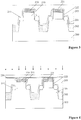
Figure 9 , after forming the second stop layer, a second planarization process may be performed to remove the dielectric layer above the capping layer (S103).Figure 5 illustrates a corresponding semiconductor structure. - Referring to
Figure 5 , after performing the second ion implantation process, a second planarization process may be performed on thedielectric layer 203 to remove thedielectric layer 203 above thecapping layer 220. When performing the second planarization process, the removal rate of the second stop layer 230 (shown inFigure 4 ) may be smaller than the removal rate of thedielectric layer 203. Therefore, thesecond stop layer 230 can protect thedielectric layer 203 over thesubstrate 200, and avoid the formation of pits in thedielectric layer 203 over thesubstrate 200 caused by too large removal rate of thedielectric layer 203. - In one embodiment, the second planarization process may also include removing the
second stop layer 230 to expose thebarrier layer 221. In one embodiment, the second planarization process performed to remove thedielectric layer 203 above thecapping layer 220 may include a chemical mechanical polishing process. - Returning to
Figure 9 , after removing the dielectric layer above the capping layer, a first ion implantation process may be performed on the dielectric layer to form a first stop layer (S104).Figure 6 illustrates a corresponding semiconductor structure. - Referring to
Figure 6 , a first ion implantation process may be performed on thedielectric layer 203 to form afirst stop layer 240 in thedielectric layer 203. The top surface of thefirst stop layer 240 may be above or coplanar with the top surface of eachdummy gate 210. The removal rate of thefirst stop layer 240 may be smaller than the removal rate of thedielectric layer 203 when subsequently performing a first planarization process. Thus, thefirst stop layer 240 may be used as a planarization stop layer when subsequently performing the first planarization process. - In one embodiment, the bottom surface of the
first stop layer 240 may be coplanar with the top surface of eachdummy gate 210. In certain embodiments, the bottom surface of thefirst stop layer 240 may be above or lower than the top surface of eachdummy gate 210. - In one embodiment, the
dummy gates 210 may be made of silicon. The implanted ions of the first ion implantation process may be silicon ions. The removal rate of thefirst stop layer 240 formed by implanting silicon ions into thedielectric layer 203 may be close to the removal rate of thedummy gates 210 when subsequently performing the first planarization process. Therefore, when performing the first planarization process, the removal rate of thefirst stop layer 240 may be low. Thefirst stop layer 240 can protect thedielectric layer 203 between theadjacent dummy gates 210, and avoid the formation of pits in thedielectric layer 203 between theadjacent dummy gates 210 caused by too large removal rate of thedielectric layer 203. - If the thickness of the
first stop layer 240 is too small, thefirst stop layer 240 cannot effectively protect thedielectric layer 203 between theadjacent dummy gates 210, and cannot effectively reduce the amount of pits formed in thedielectric layer 203 between theadjacent dummy gates 210. If the thickness of thefirst stop layer 240 is too large, it may easily waste materials and energy. Therefore, in one embodiment, the thickness of thefirst stop layer 240 may be in a range of approximately 50 nm - 100 nm. - In one embodiment, the bottom surface of the
first stop layer 240 formed by the first ion implantation process may be coplanar with the top surface of eachdummy gate 210. In one embodiment, the first planarization process may also include removing thefirst stop layer 240 to expose the top surface of eachdummy gate 210. - In one embodiment, the process doping of the first ion implantation process may include an implantation dose in a range of approximately 1.0×10¹⁴ atoms/cm3 - 6.0×10¹⁵ atoms/cm3.
- In one embodiment, the first ion implantation process may be performed after performing the second planarization process on the
dielectric layer 203. In another embodiment, the first ion implantation process may be performed before performing the second planarization process on thedielectric layer 203. For example, the first ion implantation process may be performed before performing the second ion implantation process; or the first ion implantation process may be performed after performing the second ion implantation process. - Returning to
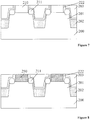
Figure 9 , after forming the first stop layer, a first planarization process may be performed to expose the top surface of each dummy gate (S105).Figure 7 illustrates a corresponding semiconductor structure. - Referring to
Figure 7 , a first planarization process may be performed on thedielectric layer 203 and thecapping layer 220 to expose the top surface of eachdummy gate 210. When performing the first planarization process, the removal rate of thefirst stop layer 240 may be smaller than the removal rate of thedielectric layer 203. Therefore, thefirst stop layer 240 can protect thedielectric layer 203 between theadjacent dummy gates 210, and avoid the formation of pits in thedielectric layer 203 between theadjacent dummy gates 210 caused by too large removal rate of thedielectric layer 203. - In one embodiment, the first planarization process performed on the
dielectric layer 203 and thecapping layer 220 may include a chemical mechanical polishing process. In one embodiment, the base substrate may include thebarrier layer 221 formed on thecapping layer 220. Thebarrier layer 221 on thecapping layer 220 may also be removed when performing the first planarization process. After performing the first planarization process, thedummy gates 210 may be removed to form trenches. - Returning to
Figure 9 , after forming the trenches, a plurality of metal gates may be formed (S106).Figure 8 illustrates a corresponding semiconductor structure. - Referring to
Figure 8 , after forming the trenches, a plurality ofmetal gates 250 may be formed in the trenches. A method for forming themetal gates 250 may include: forming a metal gate layer in the trenches and on thedielectric layer 203; and removing the metal gate layer on thedielectric layer 203. A transistor channel may be formed in eachfin 201 under eachmetal gate 250. - In one embodiment, because the surface of the
dielectric layer 203 is flat, the metal gate layer on thedielectric layer 203 may be easily removed when forming themetal gates 250. Thus, the insulation performance of thedielectric layer 203 may not be degraded. Therefore, the performance of the formed semiconductor structure may be improved. - In one embodiment, a gate-last process used to form a metal gate structure is described herein as an example. In another embodiment, the various embodiments can also be used to form a polysilicon gate transistor. The dummy gate may provide a space for forming a polysilicon gate of the polysilicon gate transistor. In certain embodiments, the various embodiments can also be used to form other semiconductor structures.
- Accordingly, the first ion implantation process may be performed on the dielectric layer to form the first stop layer before performing the first planarization process. The removal rate of the first stop layer may be smaller than the removal rate of the dielectric layer when performing the first planarization process on the dielectric layer and the capping layer. As a result, the first stop layer may be used as the planarization stop layer of the first planarization process, protect the dielectric layer under the first stop layer, and avoid the formation of pits caused by too large removal rate of the dielectric layer. Therefore, the various embodiments can improve the insulation performance of the dielectric layer over the substrate, and improve the performance of the formed semiconductor structure.
- Further, the capping layer may be made of the material different from the dielectric layer, and the dielectric layer may be above the capping layer. Before removing the dielectric layer above the capping layer, a second ion implantation process may be performed on the dielectric layer to form the second stop layer. The removal rate of the second stop layer may be smaller than the removal rate of the dielectric layer when performing the second planarization process on the dielectric layer above the capping layer. As a result, the second stop layer can avoid the formation of pits in the dielectric layer when performing the second planarization process. Therefore, the various embodiments can further improve the insulation performance of the dielectric layer over the substrate, and further improve the performance of the formed semiconductor structure.
Claims (15)
- A method for fabricating a semiconductor structure, comprising:providing a plurality of dummy gates on a substrate, a capping layer on each dummy gate, and a dielectric layer over the substrate, wherein the dielectric layer has a top surface above each dummy gate;performing a first ion implantation process on the dielectric layer to form a first stop layer in the dielectric layer, wherein a top surface of the first stop layer is above or coplanar with a top surface of each dummy gate; andperforming a first planarization process on the capping layer and the dielectric layer to expose the top surface of each dummy gate, wherein a removal rate of the first stop layer is smaller than a removal rate of the dielectric layer when performing the first planarization process.
- The method according to claim 1, wherein: the dummy gate is made of silicon; and
wherein preferably: implanted ions of the first ion implantation process are silicon ions, and an implantation dose of the first ion implantation process is in a range of approximately 1.0×10¹⁴ atoms/cm3 - 6.0×10¹⁵ atoms/cm3. - The method according to claim 1 or 2, wherein:a thickness of the first stop layer is in a range of approximately 50 nm - 100 nm; and/orthe first planarization process includes a chemical mechanical polishing process.
- The method according to anyone of the claims 1-3, wherein:the capping layer is made of a material different from the dielectric layer, andthe dielectric layer is above the capping layer.
- The method according to anyone of the claims 1-4, wherein:the capping layer is made of silicon nitride, andthe dielectric layer is made of silicon oxide.
- The method according to anyone of the claims 1-5, before performing the first planarization process, further including: performing a second planarization process on the dielectric layer to remove the dielectric layer above the capping layer.
- The method according to claim 6, wherein:the second planarization process is performed on the dielectric layer before performing the first ion implantation process; or, alternatively, the second planarization process is performed on the dielectric layer after performing the first ion implantation process.
- The method according to anyone of the claims 6 or 7, before performing the second planarization process, further including: performing a second ion implantation process on the dielectric layer to form a second stop layer, wherein a top surface of the second stop layer is above or coplanar with a top surface of the capping layer.
- The method according to claim 8, wherein:a removal rate of the second stop layer is smaller than the removal rate of the dielectric layer when performing the second planarization process.
- The method according to claim 8 or 9, wherein:a thickness of the second stop layer is in a range of approximately 50 nm - 100 nm; and/ora bottom surface of the second stop layer is coplanar with, lower than, or above the top surface of the capping layer.
- The method according to anyone of the claims 6-10, wherein:the second ion implantation process is performed before performing the first ion implantation process; or, alternatively, the second ion implantation process is performed after performing the first ion implantation process.
- The method according to anyone of the claims6-11, wherein:implanted ions of the second ion implantation process are nitrogen ions, andan implantation dose of the second ion implantation process is in a range of approximately 1.0×10¹⁴ atoms/cm3 - 6.0×10¹⁵ atoms/cm3.
- The method according to anyone of the claims 6-12, wherein the second planarization process includes: a chemical mechanical polishing process.
- The method according to anyone of the claims 1-13, wherein:a bottom surface of the first stop layer is coplanar with, lower than, or above the top surface of each dummy gate.
- The method according to anyone of the claims 1-14, after performing the first planarization process, further including:removing the plurality of dummy gates to form trenches in the dielectric layer,forming a metal gate layer in the trenches and on the dielectric layer, andremoving the metal gate layer on the dielectric layer to form a plurality of metal gates.
Applications Claiming Priority (1)
| Application Number | Priority Date | Filing Date | Title |
|---|---|---|---|
| CN201610666918.9A CN107731752B (en) | 2016-08-12 | 2016-08-12 | Method for forming semiconductor structure |
Publications (1)
| Publication Number | Publication Date |
|---|---|
| EP3282486A1 true EP3282486A1 (en) | 2018-02-14 |
Family
ID=59626464
Family Applications (1)
| Application Number | Title | Priority Date | Filing Date |
|---|---|---|---|
| EP17185879.8A Withdrawn EP3282486A1 (en) | 2016-08-12 | 2017-08-11 | Semiconductor structure and fabrication method thereof |
Country Status (3)
| Country | Link |
|---|---|
| US (1) | US10177246B2 (en) |
| EP (1) | EP3282486A1 (en) |
| CN (1) | CN107731752B (en) |
Families Citing this family (4)
| Publication number | Priority date | Publication date | Assignee | Title |
|---|---|---|---|---|
| TWI704690B (en) * | 2016-08-15 | 2020-09-11 | 聯華電子股份有限公司 | Semiconductor device and manufacturing method thereof |
| CN110648967A (en) * | 2018-06-26 | 2020-01-03 | 中芯国际集成电路制造(北京)有限公司 | Semiconductor structure and forming method thereof |
| US10692775B2 (en) * | 2018-11-09 | 2020-06-23 | Applied Materials, Inc. | Fin damage reduction during punch through implantation of FinFET device |
| CN113161285A (en) * | 2020-01-07 | 2021-07-23 | 中芯国际集成电路制造(上海)有限公司 | Semiconductor device and forming method thereof |
Citations (6)
| Publication number | Priority date | Publication date | Assignee | Title |
|---|---|---|---|---|
| US5674784A (en) * | 1996-10-02 | 1997-10-07 | Taiwan Semiconductor Manufacturing Company, Ltd. | Method for forming polish stop layer for CMP process |
| US20100163994A1 (en) * | 2008-12-31 | 2010-07-01 | Andreas Kurz | Soi device with a buried insulating material having increased etch resistivity |
| US20100330790A1 (en) * | 2009-06-30 | 2010-12-30 | Klaus Hempel | Technique for exposing a placeholder material in a replacement gate approach by modifying a removal rate of stressed dielectric overlayers |
| US8431453B2 (en) * | 2011-03-31 | 2013-04-30 | Taiwan Semiconductor Manufacturing Company, Ltd. | Plasma doping to reduce dielectric loss during removal of dummy layers in a gate structure |
| US20140124873A1 (en) * | 2012-11-07 | 2014-05-08 | International Business Machines Corporation | Robust replacement gate integration |
| CN104078357A (en) * | 2013-03-28 | 2014-10-01 | 中芯国际集成电路制造(上海)有限公司 | Method for manufacturing fin type field effect tube |
Family Cites Families (4)
| Publication number | Priority date | Publication date | Assignee | Title |
|---|---|---|---|---|
| DE10324433B4 (en) * | 2003-05-28 | 2007-02-08 | Advanced Micro Devices, Inc., Sunnyvale | A method of making a substrate contact for an SOI semiconductor device |
| CN102623405B (en) * | 2011-01-30 | 2014-08-20 | 中国科学院微电子研究所 | A method of forming a semiconductor structure |
| CN104022034B (en) * | 2013-02-28 | 2017-05-17 | 中芯国际集成电路制造(上海)有限公司 | Forming method of semiconductor structure |
| US9455330B2 (en) * | 2014-11-21 | 2016-09-27 | International Business Machines Corporation | Recessing RMG metal gate stack for forming self-aligned contact |
-
2016
- 2016-08-12 CN CN201610666918.9A patent/CN107731752B/en active Active
-
2017
- 2017-08-02 US US15/666,838 patent/US10177246B2/en active Active
- 2017-08-11 EP EP17185879.8A patent/EP3282486A1/en not_active Withdrawn
Patent Citations (6)
| Publication number | Priority date | Publication date | Assignee | Title |
|---|---|---|---|---|
| US5674784A (en) * | 1996-10-02 | 1997-10-07 | Taiwan Semiconductor Manufacturing Company, Ltd. | Method for forming polish stop layer for CMP process |
| US20100163994A1 (en) * | 2008-12-31 | 2010-07-01 | Andreas Kurz | Soi device with a buried insulating material having increased etch resistivity |
| US20100330790A1 (en) * | 2009-06-30 | 2010-12-30 | Klaus Hempel | Technique for exposing a placeholder material in a replacement gate approach by modifying a removal rate of stressed dielectric overlayers |
| US8431453B2 (en) * | 2011-03-31 | 2013-04-30 | Taiwan Semiconductor Manufacturing Company, Ltd. | Plasma doping to reduce dielectric loss during removal of dummy layers in a gate structure |
| US20140124873A1 (en) * | 2012-11-07 | 2014-05-08 | International Business Machines Corporation | Robust replacement gate integration |
| CN104078357A (en) * | 2013-03-28 | 2014-10-01 | 中芯国际集成电路制造(上海)有限公司 | Method for manufacturing fin type field effect tube |
Also Published As
| Publication number | Publication date |
|---|---|
| CN107731752B (en) | 2020-04-07 |
| CN107731752A (en) | 2018-02-23 |
| US20180047831A1 (en) | 2018-02-15 |
| US10177246B2 (en) | 2019-01-08 |
Similar Documents
| Publication | Publication Date | Title |
|---|---|---|
| CN102117750B (en) | MOSFET structure and its fabrication method | |
| CN103872132B (en) | Metal-oxide semiconductor (MOS) (MOS) transistor and preparation method thereof | |
| CN105280500B (en) | Method of forming a replacement gate structure on a semiconductor device | |
| US11081357B2 (en) | Semiconductor device and method for fabricating the same including re-growth process to form non-uniform gate dielectric layer | |
| EP3312876A1 (en) | Finfet device and fabrication method thereof | |
| CN109427582B (en) | Semiconductor structure and method of forming the same | |
| CN107919324B (en) | Method of forming a semiconductor device | |
| US20160071979A1 (en) | Fin device with blocking layer in channel region | |
| US9865505B2 (en) | Method for reducing N-type FinFET source and drain resistance | |
| EP3327788A1 (en) | Semiconductor structure, static random access memory, and fabrication method thereof | |
| US10062704B2 (en) | Buried-channel MOSFET and a surface-channel MOSFET of a same type and fabrication method thereof | |
| US20210151602A1 (en) | Semiconductor structure and fabrication method thereof | |
| EP3267476A1 (en) | Semiconductor structure and fabrication method thereof | |
| US11121237B2 (en) | Manufacturing method for FinFET device | |
| US11189711B2 (en) | Semiconductor structures | |
| US10177246B2 (en) | Semiconductor structure and fabrication method thereof | |
| EP3188245B1 (en) | Finfet and fabrication method thereof | |
| EP3244444A1 (en) | Fin-fet devices and fabrication methods thereof | |
| US9911832B2 (en) | Method to improve gate dielectric quality for FinFET | |
| US11038063B2 (en) | Semiconductor structure and fabrication method thereof | |
| CN107579108B (en) | Method for forming semiconductor structure | |
| KR20060005556A (en) | Integrated semiconductor device manufacturing method | |
| CN119342885A (en) | Semiconductor structure and method for forming the same | |
| KR100900234B1 (en) | Semiconductor device and manufacturing method thereof | |
| US20180076280A1 (en) | Shallow drain metal-oxide-semiconductor transistors |
Legal Events
| Date | Code | Title | Description |
|---|---|---|---|
| PUAI | Public reference made under article 153(3) epc to a published international application that has entered the european phase |
Free format text: ORIGINAL CODE: 0009012 |
|
| STAA | Information on the status of an ep patent application or granted ep patent |
Free format text: STATUS: THE APPLICATION HAS BEEN PUBLISHED |
|
| AK | Designated contracting states |
Kind code of ref document: A1 Designated state(s): AL AT BE BG CH CY CZ DE DK EE ES FI FR GB GR HR HU IE IS IT LI LT LU LV MC MK MT NL NO PL PT RO RS SE SI SK SM TR |
|
| AX | Request for extension of the european patent |
Extension state: BA ME |
|
| STAA | Information on the status of an ep patent application or granted ep patent |
Free format text: STATUS: REQUEST FOR EXAMINATION WAS MADE |
|
| 17P | Request for examination filed |
Effective date: 20180730 |
|
| RBV | Designated contracting states (corrected) |
Designated state(s): AL AT BE BG CH CY CZ DE DK EE ES FI FR GB GR HR HU IE IS IT LI LT LU LV MC MK MT NL NO PL PT RO RS SE SI SK SM TR |
|
| RAP1 | Party data changed (applicant data changed or rights of an application transferred) |
Owner name: SEMICONDUCTOR MANUFACTURING INTERNATIONAL (BEIJING Owner name: SEMICONDUCTOR MANUFACTURING INTERNATIONAL (SHANGHA |
|
| STAA | Information on the status of an ep patent application or granted ep patent |
Free format text: STATUS: EXAMINATION IS IN PROGRESS |
|
| 17Q | First examination report despatched |
Effective date: 20200623 |
|
| STAA | Information on the status of an ep patent application or granted ep patent |
Free format text: STATUS: THE APPLICATION HAS BEEN WITHDRAWN |
|
| 18W | Application withdrawn |
Effective date: 20201006 |