EP3282037A1 - Formation of a transition metal nitride - Google Patents
Formation of a transition metal nitride Download PDFInfo
- Publication number
- EP3282037A1 EP3282037A1 EP16183450.2A EP16183450A EP3282037A1 EP 3282037 A1 EP3282037 A1 EP 3282037A1 EP 16183450 A EP16183450 A EP 16183450A EP 3282037 A1 EP3282037 A1 EP 3282037A1
- Authority
- EP
- European Patent Office
- Prior art keywords
- transition metal
- amine
- nitride
- containing silane
- dielectric material
- Prior art date
- Legal status (The legal status is an assumption and is not a legal conclusion. Google has not performed a legal analysis and makes no representation as to the accuracy of the status listed.)
- Granted
Links
Images




Classifications
-
- H—ELECTRICITY
- H10—SEMICONDUCTOR DEVICES; ELECTRIC SOLID-STATE DEVICES NOT OTHERWISE PROVIDED FOR
- H10W—GENERIC PACKAGES, INTERCONNECTIONS, CONNECTORS OR OTHER CONSTRUCTIONAL DETAILS OF DEVICES COVERED BY CLASS H10
- H10W20/00—Interconnections in chips, wafers or substrates
- H10W20/01—Manufacture or treatment
- H10W20/031—Manufacture or treatment of conductive parts of the interconnections
- H10W20/032—Manufacture or treatment of conductive parts of the interconnections of conductive barrier, adhesion or liner layers
- H10W20/033—Manufacture or treatment of conductive parts of the interconnections of conductive barrier, adhesion or liner layers in openings in dielectrics
-
- C—CHEMISTRY; METALLURGY
- C23—COATING METALLIC MATERIAL; COATING MATERIAL WITH METALLIC MATERIAL; CHEMICAL SURFACE TREATMENT; DIFFUSION TREATMENT OF METALLIC MATERIAL; COATING BY VACUUM EVAPORATION, BY SPUTTERING, BY ION IMPLANTATION OR BY CHEMICAL VAPOUR DEPOSITION, IN GENERAL; INHIBITING CORROSION OF METALLIC MATERIAL OR INCRUSTATION IN GENERAL
- C23C—COATING METALLIC MATERIAL; COATING MATERIAL WITH METALLIC MATERIAL; SURFACE TREATMENT OF METALLIC MATERIAL BY DIFFUSION INTO THE SURFACE, BY CHEMICAL CONVERSION OR SUBSTITUTION; COATING BY VACUUM EVAPORATION, BY SPUTTERING, BY ION IMPLANTATION OR BY CHEMICAL VAPOUR DEPOSITION, IN GENERAL
- C23C16/00—Chemical coating by decomposition of gaseous compounds, without leaving reaction products of surface material in the coating, i.e. chemical vapour deposition [CVD] processes
- C23C16/02—Pretreatment of the material to be coated
- C23C16/0272—Deposition of sub-layers, e.g. to promote the adhesion of the main coating
-
- C—CHEMISTRY; METALLURGY
- C23—COATING METALLIC MATERIAL; COATING MATERIAL WITH METALLIC MATERIAL; CHEMICAL SURFACE TREATMENT; DIFFUSION TREATMENT OF METALLIC MATERIAL; COATING BY VACUUM EVAPORATION, BY SPUTTERING, BY ION IMPLANTATION OR BY CHEMICAL VAPOUR DEPOSITION, IN GENERAL; INHIBITING CORROSION OF METALLIC MATERIAL OR INCRUSTATION IN GENERAL
- C23C—COATING METALLIC MATERIAL; COATING MATERIAL WITH METALLIC MATERIAL; SURFACE TREATMENT OF METALLIC MATERIAL BY DIFFUSION INTO THE SURFACE, BY CHEMICAL CONVERSION OR SUBSTITUTION; COATING BY VACUUM EVAPORATION, BY SPUTTERING, BY ION IMPLANTATION OR BY CHEMICAL VAPOUR DEPOSITION, IN GENERAL
- C23C16/00—Chemical coating by decomposition of gaseous compounds, without leaving reaction products of surface material in the coating, i.e. chemical vapour deposition [CVD] processes
- C23C16/04—Coating on selected surface areas, e.g. using masks
- C23C16/045—Coating cavities or hollow spaces, e.g. interior of tubes; Infiltration of porous substrates
-
- C—CHEMISTRY; METALLURGY
- C23—COATING METALLIC MATERIAL; COATING MATERIAL WITH METALLIC MATERIAL; CHEMICAL SURFACE TREATMENT; DIFFUSION TREATMENT OF METALLIC MATERIAL; COATING BY VACUUM EVAPORATION, BY SPUTTERING, BY ION IMPLANTATION OR BY CHEMICAL VAPOUR DEPOSITION, IN GENERAL; INHIBITING CORROSION OF METALLIC MATERIAL OR INCRUSTATION IN GENERAL
- C23C—COATING METALLIC MATERIAL; COATING MATERIAL WITH METALLIC MATERIAL; SURFACE TREATMENT OF METALLIC MATERIAL BY DIFFUSION INTO THE SURFACE, BY CHEMICAL CONVERSION OR SUBSTITUTION; COATING BY VACUUM EVAPORATION, BY SPUTTERING, BY ION IMPLANTATION OR BY CHEMICAL VAPOUR DEPOSITION, IN GENERAL
- C23C16/00—Chemical coating by decomposition of gaseous compounds, without leaving reaction products of surface material in the coating, i.e. chemical vapour deposition [CVD] processes
- C23C16/22—Chemical coating by decomposition of gaseous compounds, without leaving reaction products of surface material in the coating, i.e. chemical vapour deposition [CVD] processes characterised by the deposition of inorganic material, other than metallic material
- C23C16/30—Deposition of compounds, mixtures or solid solutions, e.g. borides, carbides, nitrides
- C23C16/34—Nitrides
-
- C—CHEMISTRY; METALLURGY
- C23—COATING METALLIC MATERIAL; COATING MATERIAL WITH METALLIC MATERIAL; CHEMICAL SURFACE TREATMENT; DIFFUSION TREATMENT OF METALLIC MATERIAL; COATING BY VACUUM EVAPORATION, BY SPUTTERING, BY ION IMPLANTATION OR BY CHEMICAL VAPOUR DEPOSITION, IN GENERAL; INHIBITING CORROSION OF METALLIC MATERIAL OR INCRUSTATION IN GENERAL
- C23C—COATING METALLIC MATERIAL; COATING MATERIAL WITH METALLIC MATERIAL; SURFACE TREATMENT OF METALLIC MATERIAL BY DIFFUSION INTO THE SURFACE, BY CHEMICAL CONVERSION OR SUBSTITUTION; COATING BY VACUUM EVAPORATION, BY SPUTTERING, BY ION IMPLANTATION OR BY CHEMICAL VAPOUR DEPOSITION, IN GENERAL
- C23C16/00—Chemical coating by decomposition of gaseous compounds, without leaving reaction products of surface material in the coating, i.e. chemical vapour deposition [CVD] processes
- C23C16/56—After-treatment
-
- H—ELECTRICITY
- H10—SEMICONDUCTOR DEVICES; ELECTRIC SOLID-STATE DEVICES NOT OTHERWISE PROVIDED FOR
- H10W—GENERIC PACKAGES, INTERCONNECTIONS, CONNECTORS OR OTHER CONSTRUCTIONAL DETAILS OF DEVICES COVERED BY CLASS H10
- H10W20/00—Interconnections in chips, wafers or substrates
- H10W20/01—Manufacture or treatment
- H10W20/031—Manufacture or treatment of conductive parts of the interconnections
- H10W20/032—Manufacture or treatment of conductive parts of the interconnections of conductive barrier, adhesion or liner layers
- H10W20/052—Manufacture or treatment of conductive parts of the interconnections of conductive barrier, adhesion or liner layers by treatments not introducing additional elements therein
- H10W20/0526—Manufacture or treatment of conductive parts of the interconnections of conductive barrier, adhesion or liner layers by treatments not introducing additional elements therein by thermal treatment thereof
-
- H—ELECTRICITY
- H10—SEMICONDUCTOR DEVICES; ELECTRIC SOLID-STATE DEVICES NOT OTHERWISE PROVIDED FOR
- H10W—GENERIC PACKAGES, INTERCONNECTIONS, CONNECTORS OR OTHER CONSTRUCTIONAL DETAILS OF DEVICES COVERED BY CLASS H10
- H10W20/00—Interconnections in chips, wafers or substrates
- H10W20/01—Manufacture or treatment
- H10W20/031—Manufacture or treatment of conductive parts of the interconnections
- H10W20/032—Manufacture or treatment of conductive parts of the interconnections of conductive barrier, adhesion or liner layers
- H10W20/055—Manufacture or treatment of conductive parts of the interconnections of conductive barrier, adhesion or liner layers by formation methods other than physical vapour deposition [PVD], chemical vapour deposition [CVD] or liquid deposition
- H10W20/0552—Manufacture or treatment of conductive parts of the interconnections of conductive barrier, adhesion or liner layers by formation methods other than physical vapour deposition [PVD], chemical vapour deposition [CVD] or liquid deposition by diffusing metallic dopants to react with dielectrics
-
- H—ELECTRICITY
- H10—SEMICONDUCTOR DEVICES; ELECTRIC SOLID-STATE DEVICES NOT OTHERWISE PROVIDED FOR
- H10W—GENERIC PACKAGES, INTERCONNECTIONS, CONNECTORS OR OTHER CONSTRUCTIONAL DETAILS OF DEVICES COVERED BY CLASS H10
- H10W20/00—Interconnections in chips, wafers or substrates
- H10W20/01—Manufacture or treatment
- H10W20/031—Manufacture or treatment of conductive parts of the interconnections
- H10W20/056—Manufacture or treatment of conductive parts of the interconnections by filling conductive material into holes, grooves or trenches
-
- H—ELECTRICITY
- H10—SEMICONDUCTOR DEVICES; ELECTRIC SOLID-STATE DEVICES NOT OTHERWISE PROVIDED FOR
- H10W—GENERIC PACKAGES, INTERCONNECTIONS, CONNECTORS OR OTHER CONSTRUCTIONAL DETAILS OF DEVICES COVERED BY CLASS H10
- H10W20/00—Interconnections in chips, wafers or substrates
- H10W20/01—Manufacture or treatment
- H10W20/071—Manufacture or treatment of dielectric parts thereof
- H10W20/074—Manufacture or treatment of dielectric parts thereof of dielectric parts comprising thin functional dielectric layers, e.g. dielectric etch-stop, barrier, capping or liner layers
- H10W20/076—Manufacture or treatment of dielectric parts thereof of dielectric parts comprising thin functional dielectric layers, e.g. dielectric etch-stop, barrier, capping or liner layers in via holes or trenches
-
- H—ELECTRICITY
- H10—SEMICONDUCTOR DEVICES; ELECTRIC SOLID-STATE DEVICES NOT OTHERWISE PROVIDED FOR
- H10W—GENERIC PACKAGES, INTERCONNECTIONS, CONNECTORS OR OTHER CONSTRUCTIONAL DETAILS OF DEVICES COVERED BY CLASS H10
- H10W20/00—Interconnections in chips, wafers or substrates
- H10W20/01—Manufacture or treatment
- H10W20/071—Manufacture or treatment of dielectric parts thereof
- H10W20/081—Manufacture or treatment of dielectric parts thereof by forming openings in the dielectric parts
-
- H—ELECTRICITY
- H10—SEMICONDUCTOR DEVICES; ELECTRIC SOLID-STATE DEVICES NOT OTHERWISE PROVIDED FOR
- H10W—GENERIC PACKAGES, INTERCONNECTIONS, CONNECTORS OR OTHER CONSTRUCTIONAL DETAILS OF DEVICES COVERED BY CLASS H10
- H10W20/00—Interconnections in chips, wafers or substrates
- H10W20/01—Manufacture or treatment
- H10W20/071—Manufacture or treatment of dielectric parts thereof
- H10W20/093—Manufacture or treatment of dielectric parts thereof by modifying materials of the dielectric parts
- H10W20/096—Manufacture or treatment of dielectric parts thereof by modifying materials of the dielectric parts by contacting with gases, liquids or plasmas
-
- H—ELECTRICITY
- H10—SEMICONDUCTOR DEVICES; ELECTRIC SOLID-STATE DEVICES NOT OTHERWISE PROVIDED FOR
- H10W—GENERIC PACKAGES, INTERCONNECTIONS, CONNECTORS OR OTHER CONSTRUCTIONAL DETAILS OF DEVICES COVERED BY CLASS H10
- H10W20/00—Interconnections in chips, wafers or substrates
- H10W20/40—Interconnections external to wafers or substrates, e.g. back-end-of-line [BEOL] metallisations or vias connecting to gate electrodes
- H10W20/41—Interconnections external to wafers or substrates, e.g. back-end-of-line [BEOL] metallisations or vias connecting to gate electrodes characterised by their conductive parts
- H10W20/42—Vias, e.g. via plugs
-
- H—ELECTRICITY
- H10—SEMICONDUCTOR DEVICES; ELECTRIC SOLID-STATE DEVICES NOT OTHERWISE PROVIDED FOR
- H10W—GENERIC PACKAGES, INTERCONNECTIONS, CONNECTORS OR OTHER CONSTRUCTIONAL DETAILS OF DEVICES COVERED BY CLASS H10
- H10W20/00—Interconnections in chips, wafers or substrates
- H10W20/40—Interconnections external to wafers or substrates, e.g. back-end-of-line [BEOL] metallisations or vias connecting to gate electrodes
- H10W20/41—Interconnections external to wafers or substrates, e.g. back-end-of-line [BEOL] metallisations or vias connecting to gate electrodes characterised by their conductive parts
- H10W20/425—Barrier, adhesion or liner layers
Definitions
- the present invention relates to the field of transition metal nitrides and in particular to the transition metal nitrides usable in barrier layers, used in the fabrication of interconnections in integrated circuits.
- transition metal layers such as layers comprising manganese
- barrier layers are very interesting as barrier layers.
- US20110163062 A1 for example describes the use of manganese, chromium, vanadium or cobalt layers for preventing copper diffusion out of the wires.
- the significance of these transition metal layers is mainly owed to them being very conformal layers, which are self-forming and which can be scaled down to sub-2nm thickness.
- transition metal films may be either in the form of the metallic transition metal or in the form of a transition metal compound.
- silicon oxide the mechanism of manganese barrier formation involves the formation of manganese silicate.
- a low-k material however, this is much more difficult, due to a reduced number of available oxygen sites, and only happens upon annealing above 200 °C.
- the low-k material is porous, manganese easily diffuses into the pores. Apart from diffusion into the low-k material, the manganese also readily diffuses into the copper; resulting in an increased copper resistivity and a loss of barrier properties.
- transition metal compounds usable as barrier layers, where the transition metal is sufficiently immobilized in the layer.
- transition metal nitrides can be used as barrier layers for (metal) interconnects in integrated circuits. It is a further advantage of embodiments of the present invention that these (metal) interconnects may be made using a damascene process.
- a damascene process is a process where openings such as vias or trenches are cut into a dielectric material and then filled with fill metal, typically followed by removing the excess metal over the dielectric material surface, to form desired interconnect metal patterns within the openings.
- the transition metal is hindered from diffusing into a low-k material or copper, and typically both.
- the formation of the barrier layer is compatible with the use of porous low-k materials.
- the formation of the barrier layer is compatible with the use of high carbon/low oxygen low-k materials.
- the present invention relates to a use of an amine-containing silane for forming a transition metal nitride.
- the amine of the amine-containing silane is the source of at least some, preferably most and most preferably all of the nitrogen present in the transition metal nitride.
- the present invention relates to a method for forming a barrier layer against the diffusion of a fill metal, comprising the steps of:
- the present invention relates to a method for forming a barrier layer useable in a formation of interconnects, comprising the steps of:
- the present invention relates to a structure for use in a formation of interconnects, obtainable by the method according to embodiments of the second aspect.
- the present invention relates to a structure for use in a formation of interconnects, comprising:
- a barrier layer is a layer which prevents the diffusion of a material across it.
- a barrier layer in a damascene process for the formation of interconnects is a barrier layer which prevents the diffusion of a fill metal, e.g. copper, ruthenium, nickel or tungsten, into a dielectric material, e.g. a low-k material.
- a transition metal precursor is a transition metal compound serving as a source of the transition metal.
- transition metal precursors are capable of reacting with primary or secondary amino groups to form transition metal nitrides.
- the present invention relates to a use of an amine-containing silane for forming a transition metal nitride.
- the amine of the amine-containing silane is the source of at least some, preferably most and most preferably all of the nitrogen present in the transition metal nitride.
- the amine-containing silane is an organosilane and may typically comprise a primary or secondary amine functional group.
- the amine-containing silane may comprise a plurality of amine functional groups, such as a plurality of primary and/or secondary amine functional groups.
- the one or more amine functional groups comprised in a silane advantageously act as source of nitrogen for the formation of the transition metal nitride.
- the silane advantageously allows the formation of a self-assembled monolayer (SAM).
- the SAM typically has a thickness below 5nm, preferably below 1 nm.
- a layer of the silane, such as a SAM can advantageously partially seal the pores of a porous material, such as a porous low-k material, and thereby help prevent diffusion of the transition metal therein.
- the silane may be of general formula R-SiOR' 3 wherein R is a hydrocarbyl group comprising one or more primary and/or secondary amine functional groups and R' is an alkyl.
- the amine-containing silane may for example be a [3-(2-aminoethylamino)propyl]trimethoxysilane (DETA) or a (3-aminopropyl)trimethoxysilane (APTMS).
- the silane may be of general formula R-SiCl 3 wherein R is a hydrocarbyl group comprising one or more protected primary and/or secondary amine functional groups and R' is an alkyl.
- the protected primary and/or secondary amine functional groups can be later deprotected, after the -SiCl 3 group has been anchored to the substrate.
- the transition metal nitride may be a nitride of a transition metal belonging to a group from group 4 to group 9 of the periodic table of the elements, preferably from group 7 to group 9.
- the metal is selected in such a group and in a period selected from periods 4 to 6.
- the transition metal nitride may be a manganese nitride (Mn x N y ), a cobalt nitride (Co x N y ), a ruthenium nitride (Ru x N y ), a chromium nitride (Cr x N y ), a vanadium nitride (V x N y ), a titanium nitride (Ti x N y ) or a tantalum nitride (Ta x N y ).
- Mn x N y manganese nitride
- Co x N y cobalt nitride
- Ru x N y ruthenium nitride
- Cr x N y chromium nitride
- V x N y vanadium nitride
- Ti x N y titanium nitride
- Ta x N y tant
- the transition metal nitride may be a manganese nitride (Mn x N y ), a cobalt nitride (Co x N y ) or a ruthenium nitride (Ru x N y ).
- the transition metal nitride may be a manganese nitride (Mn x N y ).
- the values for X and Y can vary since typically one or more metal nitride compound are formed. For instance, in the case of manganese nitride, one or more of MnN, Mn 4 N, Mn 3 N 2 , Mn 2 N may be formed.
- Manganese nitride, cobalt nitride and ruthenium nitride are particularly useful in the formation of a barrier layer, such as a barrier layer for use in a damascene process.
- a barrier layer such as a barrier layer for use in a damascene process.
- the use of manganese compounds in barrier layers is well known within the art; the use of cobalt compounds for this purpose is emerging. Furthermore, the chemistry of both cobalt and ruthenium is similar to that of manganese.
- transition metal nitrides advantageously have better adhesion properties to dielectrics, as compared to the pure transition metal. Good adhesion is a useful property for forming a good barrier layer.
- the present invention may relate to the use of an amine-containing silane for forming a transition metal nitride forming at least part of a barrier layer against the diffusion of a fill metal in a damascene process.
- this fill metal is copper.
- the amine-containing silane may be in contact with a dielectric material.
- the amine-containing silane may form a layer, such as a SAM, in contact with the dielectric material.
- the dielectric material may be a low-k material.
- the amine-containing silane may form a layer, such as a SAM, in contact with the low-k material.
- the amine-containing silane may be chemically reacted with the dielectric material.
- the amine-containing silane may be chemically bound to the dielectric material.
- the amine-containing silane may be reacted with a dielectric material so that the silicon atom of the silane is bound to the dielectric material and the one or more amine groups are not reacted and are available for the reaction with the transition metal or transition metal precursor.
- the low-k material may be a porous low-k material.
- the low-k material may typically have a dielectric constant of 3.0 or below, preferably from 2.1 to 2.8, such as from 2.3 to 2.5.
- the dielectric material may be a silicon-based material, such as an organosilicate.
- the silicon-based low-k material may have a carbon content of 25% or more and/or an oxygen content of 10% or less; where the carbon and oxygen content are expressed in atomic percent, i.e. as the number fraction of the respective atom to the total number of atoms in the material.
- the present invention is particularly advantageous when used in combination with silicon-based low-k materials having a high carbon and/or low oxygen content.
- this type of low-k material there are otherwise typically too few reactive sites, such as oxygen sites, to directly form a good, immobilized transition metal barrier between the transition metal (compound) and the low-k material.
- high carbon content low-k materials are the current industry standard.
- the low-k material may have a hydrophilic surface.
- a hydrophilic surface of a low-k material typically comprises groups, such as hydroxide groups, which can react with the silane.
- the silane may for example form a covalent -Si-O-Si- bond with a silicon-based low-k material.
- a low-k material, such as a silicon-based low-k material may typically be made more hydrophilic by a short exposure to a CO 2 plasma.
- the formation of the transition metal nitride may comprise contacting a transition metal or transition metal precursor with the amine-containing silane. Contacting may for example be achieved by depositing the transition metal or transition metal precursor on the amine-containing silane, e.g. by means of physical vapour deposition (PVD), chemical vapour deposition (CVD) or atomic layer deposition (ALD), or by exposing the amine-containing silane to a solution comprising the transition metal or transition metal precursor, such as a solution in an organic solvent, e.g. by dipping or by spin coating.
- the formation of the transition metal nitride may comprise a chemical reaction between the transition metal or transition metal precursor and the amine-containing silane.
- the formation of the transition metal nitride may comprise annealing the transition metal or transition metal precursor after the contacting, e.g. to initiate a chemical reaction between the transition metal or transition metal precursor and the amine-containing silane.
- annealing the transition metal or transition metal precursor may be performed at a temperature from 150 °C to 450 °C, preferably from 200 °C to 400 °C.
- the transition metal may be manganese, cobalt or ruthenium.
- the transition metal precursor may be a compound, such as a manganese compound, a cobalt compound or a ruthenium compound.
- manganese amidinate could be used.
- a plurality of transition metal and/or transition metal precursors may be contacted; for example, both manganese or a manganese precursor and ruthenium or a ruthenium precursor may be contacted.
- the use may further be for spatially confining, e.g. hindering the diffusion of, a transition metal compound.
- the transition metal compound may for example be manganese, a manganese nitride, a manganese silicate or a manganese-copper compound.
- the transition metal compound may be spatially confined outside the low-k material. Spatially confining the transition metal compound advantageously maintains the good barrier properties.
- the damascene process may use a fill metal, such as copper, and the transition metal compound may be spatially confined outside the fill metal. Spatially confining the transition metal compound outside the fill metal advantageously maintains the conductivity of the fill metal.
- the present invention relates to a method for forming a barrier layer against the diffusion of a fill metal, comprising the steps of:
- step b of contacting the amine-containing silane with the dielectric material region may be reacting the amine-containing silane with the low-k material region.
- step c of reacting the transition metal or transition metal precursor with the amine-containing silane may comprise the steps c1) of contacting the transition metal or transition metal precursor with the amine containing silane, followed by c2) exposing the transition metal or transition metal precursor to a temperature above room temperature.
- this temperature may be from 150 °C to 450 °C, preferably from 200 °C to 400 °C.
- the formation of interconnects may comprise a damascene process.
- step c may be with the proviso that the transition metal precursor is not a transition metal nitride.
- the dielectric material region may comprise an exposed opening.
- it may comprise a trench or a via.
- the substrate may additionally comprise a semiconductor substrate.
- the semiconductor substrate may comprise a semiconductor device, such as a transistor or a memory device.
- Contacting the transition metal or transition metal precursor with the amine-containing silane may for example be achieved by depositing the transition metal or transition metal precursor on the amine-containing silane, e.g. by means of physical vapour deposition (PVD), chemical vapour deposition (CVD) or atomic layer deposition (ALD), or by exposing the amine-containing silane to a solution comprising the transition metal or transition metal precursor, such as a solution comprising an organic solvent, e.g. by dipping or by spin coating.
- PVD physical vapour deposition
- CVD chemical vapour deposition
- ALD atomic layer deposition
- Contacting the amine-containing silane with the dielectric material may for example be achieved by depositing the amine-containing silane on the dielectric material, e.g. by means of physical vapour deposition (PVD), chemical vapour deposition (CVD) or atomic layer deposition (ALD), or by exposing the dielectric material to a solution comprising the amine-containing silane, such as a solution comprising an organic solvent, e.g. by dipping or by spin coating.
- PVD physical vapour deposition
- CVD chemical vapour deposition
- ALD atomic layer deposition
- contacting the transition metal or the transition metal precursor with the amine-containing silane may comprise a chemical reaction between the transition metal or transition metal precursor and the amine-containing silane.
- heating up the transition metal or transition metal precursor may lead to a chemical reaction between the transition metal or transition metal precursor and the amine-containing silane.
- the chemical reaction may form a transition metal nitride.
- the transition metal may be manganese, cobalt or ruthenium.
- the transition metal precursor may be a compound, such as a manganese compound, a cobalt compound or a ruthenium compound.
- the barrier layer, the damascene process, the low-k material, the contacting, the amine-containing silane, the transition metal or transition metal precursor and the annealing may be as previously described for the first aspect.
- the present invention relates to a structure for use in a formation of interconnects, obtainable by the method according to embodiments of the second aspect.
- the present invention relates to a structure for use in a formation of interconnects, comprising:
- the present invention may relate to a structure for use in a formation of interconnects, comprising:
- the present invention may relate to a structure for use in a formation of interconnects, comprising:
- features of the third aspect may be in accordance with corresponding features of any of the previous aspects and their embodiments.
- the transition metal may be selected from cobalt and ruthenium.
- Example 1 formation of a manganese nitride barrier layer for use in a damascene process
- a plasma-enhanced chemical vapour deposited (PECVD) substrate was provided having a layer of porous silicon-based low-k material thereon.
- the porous silicon-based low-k material had a dielectric constant of 2.4.
- a pattern of trenches was defined in the layer of low-k material.
- the exposed surfaces, such as the side walls of the trenches, were then made more hydrophilic by a 2 to 3 s exposure to a CO 2 plasma.
- a SAM of DETA was formed, either from the liquid phase or from the vapour phase, on the side walls of the trenches, at least partially sealing the pores of the porous low-k material.
- manganese (example 1a) or manganese nitride (example 1b) was deposited on the SAM using chemical vapour deposition and a 200-400 °C thermal annealing was performed to complete the reaction of the manganese with the SAM; thereby forming a manganese barrier layer comprising manganese nitride.
- copper was deposited inside the trenches covered with the manganese barrier layer. This deposition was performed by means of a damascene process.
- Fig. 1 and 2 Backside secondary ion mass spectrometry (SIMS) spectra of the samples, obtained by depositing manganese nitride (example 1 b), without ( Fig. 1 ) and with ( Fig. 2 ) SAM were taken.
- the SAM was present, the presence of the Mn was bound to the manganese barrier layer and no Mn was observed in either the low-k material or in the copper layer.
- Fig. 3 to 5 Silicon ( Fig. 3 and 4 ) and nitrogen ( Fig. 5 ) XPS chemical analysis data are shown on samples, obtained by depositing manganese (example 1a), without ( Fig. 3 ) and with SAM ( Fig. 4 and 5 ) during different steps of the sample formation: a) the low-k material on SOG as loaded, further comprising the SAM (if present), b) after manganese deposition, c) after annealing at 200 °C and d) after annealing at 400 °C. In the absence of the SAM ( Fig. 3 ), no MnSiO 3 formation could be observed prior to annealing; whereas in the presence of the SAM ( Fig.
- Example 2 formation of a ruthenium nitride barrier layer for use in a damascene process
- a substrate was provided having a layer of porous organosilicate low-k material thereon.
- the low-k material had a dielectric constant of 2.4; in another, the dielectric constant was 2.55.
- a pattern of trenches and vias was defined in the layer of low-k material. The exposed surfaces, such as the side walls of the trenches, were then made more hydrophilic by a 2 to 3 s exposure to a CO 2 plasma.
- a SAM of DETA was formed, from the vapour phase, on the side walls of the trenches, at least partially sealing the pores of the porous low-k material.
- ruthenium was deposited on the SAM using atomic layer deposition and a 200-400 °C thermal annealing was performed to complete the reaction of the ruthenium with the SAM. Finally, copper was deposited inside the trenches covered with the ruthenium barrier layer. This deposition was performed by means of a (dual) damascene process.
Landscapes
- Chemical & Material Sciences (AREA)
- General Chemical & Material Sciences (AREA)
- Chemical Kinetics & Catalysis (AREA)
- Engineering & Computer Science (AREA)
- Materials Engineering (AREA)
- Mechanical Engineering (AREA)
- Metallurgy (AREA)
- Organic Chemistry (AREA)
- Inorganic Chemistry (AREA)
- Internal Circuitry In Semiconductor Integrated Circuit Devices (AREA)
Abstract
Description
- The present invention relates to the field of transition metal nitrides and in particular to the transition metal nitrides usable in barrier layers, used in the fabrication of interconnections in integrated circuits.
- Within the field of (metal) interconnect fabrication in integrated circuits, transition metal layers, such as layers comprising manganese, are very interesting as barrier layers.
US20110163062 A1 for example describes the use of manganese, chromium, vanadium or cobalt layers for preventing copper diffusion out of the wires. The significance of these transition metal layers is mainly owed to them being very conformal layers, which are self-forming and which can be scaled down to sub-2nm thickness. - These transition metal films may be either in the form of the metallic transition metal or in the form of a transition metal compound. On silicon oxide, the mechanism of manganese barrier formation involves the formation of manganese silicate. On a low-k material however, this is much more difficult, due to a reduced number of available oxygen sites, and only happens upon annealing above 200 °C. Furthermore, if the low-k material is porous, manganese easily diffuses into the pores. Apart from diffusion into the low-k material, the manganese also readily diffuses into the copper; resulting in an increased copper resistivity and a loss of barrier properties.
- There is thus still a need within the art for methods of forming transition metal compounds, usable as barrier layers, where the transition metal is sufficiently immobilized in the layer.
- It is an object of the present invention to provide good methods for forming transition metal nitrides, usable as barrier layers.
- It is an advantage of embodiments of the present invention that the transition metal nitrides can be used as barrier layers for (metal) interconnects in integrated circuits. It is a further advantage of embodiments of the present invention that these (metal) interconnects may be made using a damascene process. A damascene process is a process where openings such as vias or trenches are cut into a dielectric material and then filled with fill metal, typically followed by removing the excess metal over the dielectric material surface, to form desired interconnect metal patterns within the openings.
- It is an advantage of embodiments of the present invention that the transition metal is hindered from diffusing into a low-k material or copper, and typically both.
- It is an advantage of embodiments of the present invention that the formation of the barrier layer is compatible with the use of porous low-k materials.
- It is an advantage of embodiments of the present invention that the formation of the barrier layer is compatible with the use of high carbon/low oxygen low-k materials.
- The above objective is accomplished by a use and a method according to the present invention.
- In a first aspect, the present invention relates to a use of an amine-containing silane for forming a transition metal nitride. In this use, the amine of the amine-containing silane is the source of at least some, preferably most and most preferably all of the nitrogen present in the transition metal nitride.
- In a second aspect, the present invention relates to a method for forming a barrier layer against the diffusion of a fill metal, comprising the steps of:
- a. providing a substrate comprising a dielectric material region,
- b. contacting an amine-containing silane with the dielectric material region,
- c. reacting a transition metal or transition metal precursor with the amine-containing silane, with the proviso that the transition metal precursor is not a manganese nitride, thereby forming a transition metal nitride.
- In an embodiment, the present invention relates to a method for forming a barrier layer useable in a formation of interconnects, comprising the steps of:
- a. providing a substrate comprising a low-k material,
- b. contacting an amine-containing silane with the low-k material,
- c. contacting a transition metal or transition metal precursor with the amine-containing silane, with the proviso that the transition metal precursor is not a manganese nitride, and
- d. optionally, heating up the transition metal or transition metal precursor.
- In a third aspect, the present invention relates to a structure for use in a formation of interconnects, obtainable by the method according to embodiments of the second aspect.
- In embodiments of the third aspect, the present invention relates to a structure for use in a formation of interconnects, comprising:
- i. a substrate comprising a dielectric material region comprising an opening;
- ii. a barrier layer comprising a transition metal nitride, the barrier layer overlaying the opening and being obtainable by first contacting an amine-containing silane with the dielectric material region, and second reacting a transition metal or transition metal precursor with the amine-containing silane, with the proviso that the transition metal precursor is not a manganese nitride.
- Particular and preferred aspects of the invention are set out in the accompanying independent and dependent claims. Features from the dependent claims may be combined with features of the independent claims and with features of other dependent claims as appropriate and not merely as explicitly set out in the claims.
- Although there has been constant improvement, change and evolution of devices in this field, the present concepts are believed to represent substantial new and novel improvements, including departures from prior practices, resulting in the provision of more efficient, stable and reliable devices of this nature.
- The above and other characteristics, features and advantages of the present invention will become apparent from the following detailed description, taken in conjunction with the accompanying drawings, which illustrate, by way of example, the principles of the invention. This description is given for the sake of example only, without limiting the scope of the invention. The reference figures quoted below refer to the attached drawings.
-
-
Fig. 1 and 2 show backside secondary ion mass spectrometry (SIMS) spectra of samples without (Fig. 1 ) and with (Fig. 2 ) amine-containing silane, in accordance with an embodiment of the present invention. -
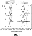
Fig. 3 to 5 show silicon (Fig. 3 and4 ) and nitrogen (Fig. 5 ) XPS chemical analysis data on samples, without (Fig. 3 ) and with (Fig. 4 and5 ) amine-containing silane, during different steps of the sample formation; in accordance with an embodiment of the present invention. -
Fig. 6 is a flowchart describing a method according to an embodiment of the third aspect of the present invention. - The present invention will be described with respect to particular embodiments and with reference to certain drawings but the invention is not limited thereto but only by the claims. The drawings described are only schematic and are non-limiting. In the drawings, the size of some of the elements may be exaggerated and not drawn on scale for illustrative purposes. The dimensions and the relative dimensions do not correspond to actual reductions to practice of the invention.
- Furthermore, the terms first, second, third and the like in the description and in the claims, are used for distinguishing between similar elements and not necessarily for describing a sequence, either temporally, spatially, in ranking or in any other manner. It is to be understood that the terms so used are interchangeable under appropriate circumstances and that the embodiments of the invention described herein are capable of operation in other sequences than described or illustrated herein.
- Moreover, the terms top, bottom, over, under and the like in the description and the claims are used for descriptive purposes and not necessarily for describing relative positions. It is to be understood that the terms so used are interchangeable under appropriate circumstances and that the embodiments of the invention described herein are capable of operation in other orientations than described or illustrated herein.
- It is to be noticed that the term "comprising", used in the claims, should not be interpreted as being restricted to the means listed thereafter; it does not exclude other elements or steps. It is thus to be interpreted as specifying the presence of the stated features, integers, steps or components as referred to, but does not preclude the presence or addition of one or more other features, integers, steps or components, or groups thereof. Thus, the scope of the expression "a device comprising means A and B" should not be limited to devices consisting only of components A and B. It means that with respect to the present invention, the only relevant components of the device are A and B.
- Reference throughout this specification to "one embodiment" or "an embodiment" means that a particular feature, structure or characteristic described in connection with the embodiment is included in at least one embodiment of the present invention. Thus, appearances of the phrases "in one embodiment" or "in an embodiment" in various places throughout this specification are not necessarily all referring to the same embodiment, but may. Furthermore, the particular features, structures or characteristics may be combined in any suitable manner, as would be apparent to one of ordinary skill in the art from this disclosure, in one or more embodiments.
- Similarly, it should be appreciated that in the description of exemplary embodiments of the invention, various features of the invention are sometimes grouped together in a single embodiment, figure, or description thereof for the purpose of streamlining the disclosure and aiding in the understanding of one or more of the various inventive aspects. This method of disclosure, however, is not to be interpreted as reflecting an intention that the claimed invention requires more features than are expressly recited in each claim. Rather, as the following claims reflect, inventive aspects lie in less than all features of a single foregoing disclosed embodiment. Thus, the claims following the detailed description are hereby expressly incorporated into this detailed description, with each claim standing on its own as a separate embodiment of this invention.
- Furthermore, while some embodiments described herein include some but not other features included in other embodiments, combinations of features of different embodiments are meant to be within the scope of the invention, and form different embodiments, as would be understood by those in the art. For example, in the following claims, any of the claimed embodiments can be used in any combination.
- In the description provided herein, numerous specific details are set forth. However, it is understood that embodiments of the invention may be practiced without these specific details. In other instances, well-known methods, structures and techniques have not been shown in detail in order not to obscure an understanding of this description.
- The following terms are provided solely to aid in the understanding of the invention.
- As used herein, and unless provided otherwise, a barrier layer is a layer which prevents the diffusion of a material across it. In particular, a barrier layer in a damascene process for the formation of interconnects is a barrier layer which prevents the diffusion of a fill metal, e.g. copper, ruthenium, nickel or tungsten, into a dielectric material, e.g. a low-k material.
- As used herein, and unless provided otherwise, a transition metal precursor is a transition metal compound serving as a source of the transition metal. In the present invention, transition metal precursors are capable of reacting with primary or secondary amino groups to form transition metal nitrides.
- In a first aspect, the present invention relates to a use of an amine-containing silane for forming a transition metal nitride. In this use, the amine of the amine-containing silane is the source of at least some, preferably most and most preferably all of the nitrogen present in the transition metal nitride.
- The amine-containing silane is an organosilane and may typically comprise a primary or secondary amine functional group. In preferred embodiments, the amine-containing silane may comprise a plurality of amine functional groups, such as a plurality of primary and/or secondary amine functional groups. It was surprisingly found within the present invention that the one or more amine functional groups comprised in a silane advantageously act as source of nitrogen for the formation of the transition metal nitride. The silane advantageously allows the formation of a self-assembled monolayer (SAM). The SAM typically has a thickness below 5nm, preferably below 1 nm. A layer of the silane, such as a SAM, can advantageously partially seal the pores of a porous material, such as a porous low-k material, and thereby help prevent diffusion of the transition metal therein.
- In embodiments, the silane may be of general formula R-SiOR'3 wherein R is a hydrocarbyl group comprising one or more primary and/or secondary amine functional groups and R' is an alkyl. The amine-containing silane may for example be a [3-(2-aminoethylamino)propyl]trimethoxysilane (DETA) or a (3-aminopropyl)trimethoxysilane (APTMS). In other embodiments, the silane may be of general formula R-SiCl3 wherein R is a hydrocarbyl group comprising one or more protected primary and/or secondary amine functional groups and R' is an alkyl. In these other embodiments, the protected primary and/or secondary amine functional groups can be later deprotected, after the -SiCl3 group has been anchored to the substrate.
- In embodiments, the transition metal nitride may be a nitride of a transition metal belonging to a group from
group 4 to group 9 of the periodic table of the elements, preferably from group 7 to group 9. In preferred embodiments, the metal is selected in such a group and in a period selected fromperiods 4 to 6. - In embodiments, the transition metal nitride may be a manganese nitride (MnxNy), a cobalt nitride (CoxNy), a ruthenium nitride (RuxNy), a chromium nitride (CrxNy), a vanadium nitride (VxNy), a titanium nitride (TixNy) or a tantalum nitride (TaxNy). In preferred embodiments, the transition metal nitride may be a manganese nitride (MnxNy), a cobalt nitride (CoxNy) or a ruthenium nitride (RuxNy). In yet more preferred embodiments, the transition metal nitride may be a manganese nitride (MnxNy). The values for X and Y can vary since typically one or more metal nitride compound are formed. For instance, in the case of manganese nitride, one or more of MnN, Mn4N, Mn3N2, Mn2N may be formed. Manganese nitride, cobalt nitride and ruthenium nitride are particularly useful in the formation of a barrier layer, such as a barrier layer for use in a damascene process. The use of manganese compounds in barrier layers is well known within the art; the use of cobalt compounds for this purpose is emerging. Furthermore, the chemistry of both cobalt and ruthenium is similar to that of manganese. It is well known within the art that transition metal nitrides advantageously have better adhesion properties to dielectrics, as compared to the pure transition metal. Good adhesion is a useful property for forming a good barrier layer. In embodiments, the present invention may relate to the use of an amine-containing silane for forming a transition metal nitride forming at least part of a barrier layer against the diffusion of a fill metal in a damascene process. In preferred embodiments, this fill metal is copper.
- In embodiments, the amine-containing silane may be in contact with a dielectric material. For example, the amine-containing silane may form a layer, such as a SAM, in contact with the dielectric material. In preferred embodiments, the dielectric material may be a low-k material. For example, the amine-containing silane may form a layer, such as a SAM, in contact with the low-k material. Typically, the amine-containing silane may be chemically reacted with the dielectric material. Typically, the amine-containing silane may be chemically bound to the dielectric material. In embodiments, the amine-containing silane may be reacted with a dielectric material so that the silicon atom of the silane is bound to the dielectric material and the one or more amine groups are not reacted and are available for the reaction with the transition metal or transition metal precursor. In embodiments, the low-k material may be a porous low-k material. The low-k material may typically have a dielectric constant of 3.0 or below, preferably from 2.1 to 2.8, such as from 2.3 to 2.5. In embodiments, the dielectric material may be a silicon-based material, such as an organosilicate. In embodiments, the silicon-based low-k material may have a carbon content of 25% or more and/or an oxygen content of 10% or less; where the carbon and oxygen content are expressed in atomic percent, i.e. as the number fraction of the respective atom to the total number of atoms in the material. The present invention is particularly advantageous when used in combination with silicon-based low-k materials having a high carbon and/or low oxygen content. In this type of low-k material, there are otherwise typically too few reactive sites, such as oxygen sites, to directly form a good, immobilized transition metal barrier between the transition metal (compound) and the low-k material. Furthermore, high carbon content low-k materials are the current industry standard. In preferred embodiments, the low-k material may have a hydrophilic surface. A hydrophilic surface of a low-k material typically comprises groups, such as hydroxide groups, which can react with the silane. The silane may for example form a covalent -Si-O-Si- bond with a silicon-based low-k material. A low-k material, such as a silicon-based low-k material, may typically be made more hydrophilic by a short exposure to a CO2 plasma.
- In embodiments, the formation of the transition metal nitride may comprise contacting a transition metal or transition metal precursor with the amine-containing silane. Contacting may for example be achieved by depositing the transition metal or transition metal precursor on the amine-containing silane, e.g. by means of physical vapour deposition (PVD), chemical vapour deposition (CVD) or atomic layer deposition (ALD), or by exposing the amine-containing silane to a solution comprising the transition metal or transition metal precursor, such as a solution in an organic solvent, e.g. by dipping or by spin coating. In embodiments, the formation of the transition metal nitride may comprise a chemical reaction between the transition metal or transition metal precursor and the amine-containing silane. In embodiments, the formation of the transition metal nitride may comprise annealing the transition metal or transition metal precursor after the contacting, e.g. to initiate a chemical reaction between the transition metal or transition metal precursor and the amine-containing silane. In embodiments, annealing the transition metal or transition metal precursor may be performed at a temperature from 150 °C to 450 °C, preferably from 200 °C to 400 °C. In preferred embodiments, the transition metal may be manganese, cobalt or ruthenium. In other embodiments, the transition metal precursor may be a compound, such as a manganese compound, a cobalt compound or a ruthenium compound. As an example of manganese compound, manganese amidinate could be used. In some embodiments, a plurality of transition metal and/or transition metal precursors may be contacted; for example, both manganese or a manganese precursor and ruthenium or a ruthenium precursor may be contacted.
- In embodiments, the use may further be for spatially confining, e.g. hindering the diffusion of, a transition metal compound. The transition metal compound may for example be manganese, a manganese nitride, a manganese silicate or a manganese-copper compound. In embodiments, the transition metal compound may be spatially confined outside the low-k material. Spatially confining the transition metal compound advantageously maintains the good barrier properties. In embodiments, the damascene process may use a fill metal, such as copper, and the transition metal compound may be spatially confined outside the fill metal. Spatially confining the transition metal compound outside the fill metal advantageously maintains the conductivity of the fill metal.
- In a second aspect (
Fig. 6 ), the present invention relates to a method for forming a barrier layer against the diffusion of a fill metal, comprising the steps of: - a. providing a substrate comprising a dielectric material region,
- b. contacting an amine-containing silane with the dielectric material region,
- c. reacting a transition metal or transition metal precursor with the amine-containing silane, with the proviso that the transition metal precursor is not a manganese nitride, thereby forming a transition metal nitride.
- In embodiments, step b of contacting the amine-containing silane with the dielectric material region may be reacting the amine-containing silane with the low-k material region.
- In embodiments, step c of reacting the transition metal or transition metal precursor with the amine-containing silane may comprise the steps c1) of contacting the transition metal or transition metal precursor with the amine containing silane, followed by c2) exposing the transition metal or transition metal precursor to a temperature above room temperature.
- In embodiments, this temperature may be from 150 °C to 450 °C, preferably from 200 °C to 400 °C.
- In embodiments, the formation of interconnects may comprise a damascene process.
- In embodiments, step c may be with the proviso that the transition metal precursor is not a transition metal nitride.
- In embodiments, the dielectric material region may comprise an exposed opening. For instance, it may comprise a trench or a via.
- In embodiments, the substrate may additionally comprise a semiconductor substrate. In embodiments, the semiconductor substrate may comprise a semiconductor device, such as a transistor or a memory device.
- Contacting the transition metal or transition metal precursor with the amine-containing silane may for example be achieved by depositing the transition metal or transition metal precursor on the amine-containing silane, e.g. by means of physical vapour deposition (PVD), chemical vapour deposition (CVD) or atomic layer deposition (ALD), or by exposing the amine-containing silane to a solution comprising the transition metal or transition metal precursor, such as a solution comprising an organic solvent, e.g. by dipping or by spin coating.
- Contacting the amine-containing silane with the dielectric material may for example be achieved by depositing the amine-containing silane on the dielectric material, e.g. by means of physical vapour deposition (PVD), chemical vapour deposition (CVD) or atomic layer deposition (ALD), or by exposing the dielectric material to a solution comprising the amine-containing silane, such as a solution comprising an organic solvent, e.g. by dipping or by spin coating.
- In embodiments, contacting the transition metal or the transition metal precursor with the amine-containing silane may comprise a chemical reaction between the transition metal or transition metal precursor and the amine-containing silane. In embodiments, heating up the transition metal or transition metal precursor may lead to a chemical reaction between the transition metal or transition metal precursor and the amine-containing silane. In embodiments, the chemical reaction may form a transition metal nitride. In preferred embodiments, the transition metal may be manganese, cobalt or ruthenium. In other embodiments, the transition metal precursor may be a compound, such as a manganese compound, a cobalt compound or a ruthenium compound.
- In embodiments, the barrier layer, the damascene process, the low-k material, the contacting, the amine-containing silane, the transition metal or transition metal precursor and the annealing may be as previously described for the first aspect.
- In a third aspect, the present invention relates to a structure for use in a formation of interconnects, obtainable by the method according to embodiments of the second aspect.
- In embodiments of the third aspect, the present invention relates to a structure for use in a formation of interconnects, comprising:
- i. a substrate comprising a dielectric material region comprising an opening;
- ii. a barrier layer comprising a transition metal nitride, the barrier layer overlaying the opening and being obtainable by first contacting an amine-containing silane with the dielectric material region, and second reacting a transition metal or transition metal precursor with the amine-containing silane, with the proviso that the transition metal precursor is not a manganese nitride.
- In an embodiment of the third aspect, the present invention may relate to a structure for use in a formation of interconnects, comprising:
- i. a substrate comprising a low-k material, the low-k material having a pattern defined therein and thereby comprising at least one opening;
- ii. a layer of amine-containing silane covering the low-k material in the at least one opening;
- iii. a barrier layer comprising at least a transition metal nitride other than manganese nitride covering the layer of amine-containing silane in the at least one opening.
- In an embodiment of the third aspect, the present invention may relate to a structure for use in a formation of interconnects, comprising:
- i. a substrate comprising a low-k material, the low-k material having a pattern defined therein and thereby comprising at least one opening;
- ii. a layer of amine-containing silane covering the low-k material in the at least one opening;
- iii. a barrier layer comprising at least a cobalt nitride or a ruthenium nitride covering the layer of amine-containing silane in the at least one opening.
- In embodiments, features of the third aspect may be in accordance with corresponding features of any of the previous aspects and their embodiments.
- In a particular embodiment, the transition metal may be selected from cobalt and ruthenium.
- The invention will now be described by a detailed description of several embodiments of the invention. It is clear that other embodiments of the invention can be configured according to the knowledge of the person skilled in the art without departing from the true technical teaching of the invention, the invention being limited only by the terms of the appended claims.
- A plasma-enhanced chemical vapour deposited (PECVD) substrate was provided having a layer of porous silicon-based low-k material thereon. The porous silicon-based low-k material had a dielectric constant of 2.4. A pattern of trenches was defined in the layer of low-k material. The exposed surfaces, such as the side walls of the trenches, were then made more hydrophilic by a 2 to 3 s exposure to a CO2 plasma. A SAM of DETA was formed, either from the liquid phase or from the vapour phase, on the side walls of the trenches, at least partially sealing the pores of the porous low-k material. Subsequently, manganese (example 1a) or manganese nitride (example 1b) was deposited on the SAM using chemical vapour deposition and a 200-400 °C thermal annealing was performed to complete the reaction of the manganese with the SAM; thereby forming a manganese barrier layer comprising manganese nitride. Finally, copper was deposited inside the trenches covered with the manganese barrier layer. This deposition was performed by means of a damascene process.
- For comparison, the same process was repeated but the SAM was omitted.
- We now refer to
Fig. 1 and 2 . Backside secondary ion mass spectrometry (SIMS) spectra of the samples, obtained by depositing manganese nitride (example 1 b), without (Fig. 1 ) and with (Fig. 2 ) SAM were taken. The presence of Mn in both the low-k material and the copper layer, i.e. outside the manganese barrier layer, was observed when no SAM was present. Conversely, when the SAM was present, the presence of the Mn was bound to the manganese barrier layer and no Mn was observed in either the low-k material or in the copper layer. These results show that the presence of the SAM leads to the spatial confinement of Mn inside the barrier layer. This result is also expected for example 1 a since in that case MnxNy is formed in situ in presence of the same SAM. - We now refer to
Fig. 3 to 5 . Silicon (Fig. 3 and4 ) and nitrogen (Fig. 5 ) XPS chemical analysis data are shown on samples, obtained by depositing manganese (example 1a), without (Fig. 3 ) and with SAM (Fig. 4 and5 ) during different steps of the sample formation: a) the low-k material on SOG as loaded, further comprising the SAM (if present), b) after manganese deposition, c) after annealing at 200 °C and d) after annealing at 400 °C. In the absence of the SAM (Fig. 3 ), no MnSiO3 formation could be observed prior to annealing; whereas in the presence of the SAM (Fig. 4 ) already some MnSiO3 formation could be observed upon manganese deposition, further increasing after annealing. Similarly, in the presence of the SAM, MnxNy is formed upon manganese deposition, with a slight additional increase after annealing. These results indicate the confinement of the manganese to the dielectric/barrier interface and improved manganese silicate formation in the presence of the SAM. - A substrate was provided having a layer of porous organosilicate low-k material thereon. In one case, the low-k material had a dielectric constant of 2.4; in another, the dielectric constant was 2.55. A pattern of trenches and vias was defined in the layer of low-k material. The exposed surfaces, such as the side walls of the trenches, were then made more hydrophilic by a 2 to 3 s exposure to a CO2 plasma. A SAM of DETA was formed, from the vapour phase, on the side walls of the trenches, at least partially sealing the pores of the porous low-k material. Subsequently, a 20-25 nm thick layer of ruthenium was deposited on the SAM using atomic layer deposition and a 200-400 °C thermal annealing was performed to complete the reaction of the ruthenium with the SAM. Finally, copper was deposited inside the trenches covered with the ruthenium barrier layer. This deposition was performed by means of a (dual) damascene process.
- It is to be understood that although preferred embodiments, specific constructions and configurations, as well as materials, have been discussed herein for devices according to the present invention, various changes or modifications in form and detail may be made without departing from the scope and technical teachings of this invention. For example, any formulas given above are merely representative of procedures that may be used. Functionality may be added or deleted from the block diagrams and operations may be interchanged among functional blocks. Steps may be added or deleted to methods described within the scope of the present invention.
Claims (17)
- Use of an amine-containing silane for forming a transition metal nitride.
- The use according to claim 1, wherein the transition metal nitride is a manganese nitride, a cobalt nitride or a ruthenium nitride.
- The use according to claim 1 or 2, wherein the amine-containing silane is in contact with a dielectric material, preferably a low-k dielectric material.
- The use according to claim 3, wherein the dielectric material is a silicon-based low-k material.
- The use according to claim 4, wherein the silicon-based low-k material has a carbon content of 25 at.% or more.
- The use according to claim 4 or 5, wherein the silicon-based low-k material has an oxygen content of 10 at.% or lower.
- The use according to any of the previous claims, wherein the transition metal nitride forms at least part of a barrier layer against the diffusion of a fill metal in a damascene process.
- The use according to claim 7, wherein the fill metal is copper.
- The use according to any of the previous claims, wherein the amine-containing silane is [3-(2-aminoethylamino)propyl]trimethoxysilane or (3-aminopropyl)trimethoxysilane.
- A method for forming a barrier layer against the diffusion of a fill metal, comprising the steps of:a. providing a substrate comprising a dielectric material region,b. contacting an amine-containing silane with the dielectric material region,c. reacting a transition metal or transition metal precursor with the amine-containing silane, with the proviso that the transition metal precursor is not a manganese nitride, thereby forming a transition metal nitride.
- The method according to claim 10, wherein the dielectric material region comprises an exposed opening.
- The method according to claim 10 or claim 11, wherein step c of reacting the transition metal or transition metal precursor with the amine-containing silane comprises the steps c1) of contacting the transition metal or transition metal precursor with the amine containing silane, followed by c2) exposing the transition metal or transition metal precursor to a temperature above room temperature.
- The method according to claim 12, wherein the temperature is from 150 °C to 450 °C, preferably from 200 °C to 400 °C.
- The method according to any of claims 10 to 13, wherein the transition metal is manganese, cobalt or ruthenium.
- The method according to any one of claims 10 to 14, wherein the dielectric material region is a low-k dielectric material region
- A structure for use in a formation of interconnects, comprising:i. a substrate comprising a dielectric material region comprising an opening;ii. a barrier layer comprising a transition metal nitride, the barrier layer overlaying the opening and being obtainable by first contacting an amine-containing silane with the dielectric material region, and second reacting a transition metal or transition metal precursor with the amine-containing silane, with the proviso that the transition metal precursor is not a manganese nitride.
- The structure according to claim 16, wherein the transition metal is selected from cobalt and ruthenium.
Priority Applications (2)
| Application Number | Priority Date | Filing Date | Title |
|---|---|---|---|
| EP16183450.2A EP3282037B1 (en) | 2016-08-09 | 2016-08-09 | Formation of a transition metal nitride |
| US15/659,507 US10262896B2 (en) | 2016-08-09 | 2017-07-25 | Formation of a transition metal nitride |
Applications Claiming Priority (1)
| Application Number | Priority Date | Filing Date | Title |
|---|---|---|---|
| EP16183450.2A EP3282037B1 (en) | 2016-08-09 | 2016-08-09 | Formation of a transition metal nitride |
Publications (2)
| Publication Number | Publication Date |
|---|---|
| EP3282037A1 true EP3282037A1 (en) | 2018-02-14 |
| EP3282037B1 EP3282037B1 (en) | 2022-12-07 |
Family
ID=56686665
Family Applications (1)
| Application Number | Title | Priority Date | Filing Date |
|---|---|---|---|
| EP16183450.2A Active EP3282037B1 (en) | 2016-08-09 | 2016-08-09 | Formation of a transition metal nitride |
Country Status (2)
| Country | Link |
|---|---|
| US (1) | US10262896B2 (en) |
| EP (1) | EP3282037B1 (en) |
Families Citing this family (239)
| Publication number | Priority date | Publication date | Assignee | Title |
|---|---|---|---|---|
| US20130023129A1 (en) | 2011-07-20 | 2013-01-24 | Asm America, Inc. | Pressure transmitter for a semiconductor processing environment |
| US20160376700A1 (en) | 2013-02-01 | 2016-12-29 | Asm Ip Holding B.V. | System for treatment of deposition reactor |
| US10858737B2 (en) | 2014-07-28 | 2020-12-08 | Asm Ip Holding B.V. | Showerhead assembly and components thereof |
| US10941490B2 (en) | 2014-10-07 | 2021-03-09 | Asm Ip Holding B.V. | Multiple temperature range susceptor, assembly, reactor and system including the susceptor, and methods of using the same |
| US10276355B2 (en) | 2015-03-12 | 2019-04-30 | Asm Ip Holding B.V. | Multi-zone reactor, system including the reactor, and method of using the same |
| US11139308B2 (en) | 2015-12-29 | 2021-10-05 | Asm Ip Holding B.V. | Atomic layer deposition of III-V compounds to form V-NAND devices |
| US10529554B2 (en) | 2016-02-19 | 2020-01-07 | Asm Ip Holding B.V. | Method for forming silicon nitride film selectively on sidewalls or flat surfaces of trenches |
| US10343920B2 (en) | 2016-03-18 | 2019-07-09 | Asm Ip Holding B.V. | Aligned carbon nanotubes |
| US11453943B2 (en) | 2016-05-25 | 2022-09-27 | Asm Ip Holding B.V. | Method for forming carbon-containing silicon/metal oxide or nitride film by ALD using silicon precursor and hydrocarbon precursor |
| US10612137B2 (en) | 2016-07-08 | 2020-04-07 | Asm Ip Holdings B.V. | Organic reactants for atomic layer deposition |
| US9859151B1 (en) | 2016-07-08 | 2018-01-02 | Asm Ip Holding B.V. | Selective film deposition method to form air gaps |
| US9887082B1 (en) | 2016-07-28 | 2018-02-06 | Asm Ip Holding B.V. | Method and apparatus for filling a gap |
| US9812320B1 (en) | 2016-07-28 | 2017-11-07 | Asm Ip Holding B.V. | Method and apparatus for filling a gap |
| US11532757B2 (en) | 2016-10-27 | 2022-12-20 | Asm Ip Holding B.V. | Deposition of charge trapping layers |
| US10714350B2 (en) | 2016-11-01 | 2020-07-14 | ASM IP Holdings, B.V. | Methods for forming a transition metal niobium nitride film on a substrate by atomic layer deposition and related semiconductor device structures |
| KR102546317B1 (en) | 2016-11-15 | 2023-06-21 | 에이에스엠 아이피 홀딩 비.브이. | Gas supply unit and substrate processing apparatus including the same |
| US11581186B2 (en) | 2016-12-15 | 2023-02-14 | Asm Ip Holding B.V. | Sequential infiltration synthesis apparatus |
| US11447861B2 (en) | 2016-12-15 | 2022-09-20 | Asm Ip Holding B.V. | Sequential infiltration synthesis apparatus and a method of forming a patterned structure |
| US11390950B2 (en) | 2017-01-10 | 2022-07-19 | Asm Ip Holding B.V. | Reactor system and method to reduce residue buildup during a film deposition process |
| US10468261B2 (en) | 2017-02-15 | 2019-11-05 | Asm Ip Holding B.V. | Methods for forming a metallic film on a substrate by cyclical deposition and related semiconductor device structures |
| US10770286B2 (en) | 2017-05-08 | 2020-09-08 | Asm Ip Holdings B.V. | Methods for selectively forming a silicon nitride film on a substrate and related semiconductor device structures |
| US12040200B2 (en) | 2017-06-20 | 2024-07-16 | Asm Ip Holding B.V. | Semiconductor processing apparatus and methods for calibrating a semiconductor processing apparatus |
| US11306395B2 (en) | 2017-06-28 | 2022-04-19 | Asm Ip Holding B.V. | Methods for depositing a transition metal nitride film on a substrate by atomic layer deposition and related deposition apparatus |
| US11114347B2 (en) * | 2017-06-30 | 2021-09-07 | Taiwan Semiconductor Manufacturing Co., Ltd. | Self-protective layer formed on high-k dielectric layers with different materials |
| KR20190009245A (en) | 2017-07-18 | 2019-01-28 | 에이에스엠 아이피 홀딩 비.브이. | Methods for forming a semiconductor device structure and related semiconductor device structures |
| US11374112B2 (en) | 2017-07-19 | 2022-06-28 | Asm Ip Holding B.V. | Method for depositing a group IV semiconductor and related semiconductor device structures |
| US10590535B2 (en) | 2017-07-26 | 2020-03-17 | Asm Ip Holdings B.V. | Chemical treatment, deposition and/or infiltration apparatus and method for using the same |
| TWI815813B (en) | 2017-08-04 | 2023-09-21 | 荷蘭商Asm智慧財產控股公司 | Showerhead assembly for distributing a gas within a reaction chamber |
| US10692741B2 (en) | 2017-08-08 | 2020-06-23 | Asm Ip Holdings B.V. | Radiation shield |
| US10770336B2 (en) | 2017-08-08 | 2020-09-08 | Asm Ip Holding B.V. | Substrate lift mechanism and reactor including same |
| US11769682B2 (en) | 2017-08-09 | 2023-09-26 | Asm Ip Holding B.V. | Storage apparatus for storing cassettes for substrates and processing apparatus equipped therewith |
| US11830730B2 (en) | 2017-08-29 | 2023-11-28 | Asm Ip Holding B.V. | Layer forming method and apparatus |
| US11295980B2 (en) | 2017-08-30 | 2022-04-05 | Asm Ip Holding B.V. | Methods for depositing a molybdenum metal film over a dielectric surface of a substrate by a cyclical deposition process and related semiconductor device structures |
| US10658205B2 (en) | 2017-09-28 | 2020-05-19 | Asm Ip Holdings B.V. | Chemical dispensing apparatus and methods for dispensing a chemical to a reaction chamber |
| US10403504B2 (en) | 2017-10-05 | 2019-09-03 | Asm Ip Holding B.V. | Method for selectively depositing a metallic film on a substrate |
| US10923344B2 (en) | 2017-10-30 | 2021-02-16 | Asm Ip Holding B.V. | Methods for forming a semiconductor structure and related semiconductor structures |
| JP7206265B2 (en) | 2017-11-27 | 2023-01-17 | エーエスエム アイピー ホールディング ビー.ブイ. | Equipment with a clean mini-environment |
| CN111316417B (en) | 2017-11-27 | 2023-12-22 | 阿斯莫Ip控股公司 | Storage device for use with batch furnaces for storing wafer cassettes |
| US10872771B2 (en) | 2018-01-16 | 2020-12-22 | Asm Ip Holding B. V. | Method for depositing a material film on a substrate within a reaction chamber by a cyclical deposition process and related device structures |
| CN111630203A (en) | 2018-01-19 | 2020-09-04 | Asm Ip私人控股有限公司 | Method of depositing a gap fill layer by plasma assisted deposition |
| TWI799494B (en) | 2018-01-19 | 2023-04-21 | 荷蘭商Asm 智慧財產控股公司 | Deposition method |
| US11081345B2 (en) | 2018-02-06 | 2021-08-03 | Asm Ip Holding B.V. | Method of post-deposition treatment for silicon oxide film |
| US10896820B2 (en) | 2018-02-14 | 2021-01-19 | Asm Ip Holding B.V. | Method for depositing a ruthenium-containing film on a substrate by a cyclical deposition process |
| JP7124098B2 (en) | 2018-02-14 | 2022-08-23 | エーエスエム・アイピー・ホールディング・ベー・フェー | Method for depositing a ruthenium-containing film on a substrate by a cyclical deposition process |
| US10731249B2 (en) | 2018-02-15 | 2020-08-04 | Asm Ip Holding B.V. | Method of forming a transition metal containing film on a substrate by a cyclical deposition process, a method for supplying a transition metal halide compound to a reaction chamber, and related vapor deposition apparatus |
| KR102636427B1 (en) | 2018-02-20 | 2024-02-13 | 에이에스엠 아이피 홀딩 비.브이. | Substrate processing method and apparatus |
| US10975470B2 (en) | 2018-02-23 | 2021-04-13 | Asm Ip Holding B.V. | Apparatus for detecting or monitoring for a chemical precursor in a high temperature environment |
| US11473195B2 (en) | 2018-03-01 | 2022-10-18 | Asm Ip Holding B.V. | Semiconductor processing apparatus and a method for processing a substrate |
| KR102646467B1 (en) | 2018-03-27 | 2024-03-11 | 에이에스엠 아이피 홀딩 비.브이. | Method of forming an electrode on a substrate and a semiconductor device structure including an electrode |
| KR102600229B1 (en) | 2018-04-09 | 2023-11-10 | 에이에스엠 아이피 홀딩 비.브이. | Substrate supporting device, substrate processing apparatus including the same and substrate processing method |
| US12025484B2 (en) | 2018-05-08 | 2024-07-02 | Asm Ip Holding B.V. | Thin film forming method |
| US12272527B2 (en) | 2018-05-09 | 2025-04-08 | Asm Ip Holding B.V. | Apparatus for use with hydrogen radicals and method of using same |
| KR102596988B1 (en) | 2018-05-28 | 2023-10-31 | 에이에스엠 아이피 홀딩 비.브이. | Method of processing a substrate and a device manufactured by the same |
| US11718913B2 (en) | 2018-06-04 | 2023-08-08 | Asm Ip Holding B.V. | Gas distribution system and reactor system including same |
| US10797133B2 (en) | 2018-06-21 | 2020-10-06 | Asm Ip Holding B.V. | Method for depositing a phosphorus doped silicon arsenide film and related semiconductor device structures |
| KR102568797B1 (en) | 2018-06-21 | 2023-08-21 | 에이에스엠 아이피 홀딩 비.브이. | Substrate processing system |
| KR20250134000A (en) | 2018-06-27 | 2025-09-09 | 에이에스엠 아이피 홀딩 비.브이. | Cyclic deposition methods for forming metal-containing material and films and structures including the metal-containing material |
| US11499222B2 (en) | 2018-06-27 | 2022-11-15 | Asm Ip Holding B.V. | Cyclic deposition methods for forming metal-containing material and films and structures including the metal-containing material |
| US10755922B2 (en) | 2018-07-03 | 2020-08-25 | Asm Ip Holding B.V. | Method for depositing silicon-free carbon-containing film as gap-fill layer by pulse plasma-assisted deposition |
| US10388513B1 (en) | 2018-07-03 | 2019-08-20 | Asm Ip Holding B.V. | Method for depositing silicon-free carbon-containing film as gap-fill layer by pulse plasma-assisted deposition |
| US11053591B2 (en) | 2018-08-06 | 2021-07-06 | Asm Ip Holding B.V. | Multi-port gas injection system and reactor system including same |
| US11430674B2 (en) | 2018-08-22 | 2022-08-30 | Asm Ip Holding B.V. | Sensor array, apparatus for dispensing a vapor phase reactant to a reaction chamber and related methods |
| US11024523B2 (en) | 2018-09-11 | 2021-06-01 | Asm Ip Holding B.V. | Substrate processing apparatus and method |
| KR102707956B1 (en) | 2018-09-11 | 2024-09-19 | 에이에스엠 아이피 홀딩 비.브이. | Method for deposition of a thin film |
| CN110970344B (en) | 2018-10-01 | 2024-10-25 | Asmip控股有限公司 | Substrate holding device, system including the same and method of using the same |
| KR102592699B1 (en) | 2018-10-08 | 2023-10-23 | 에이에스엠 아이피 홀딩 비.브이. | Substrate support unit and apparatuses for depositing thin film and processing the substrate including the same |
| KR102546322B1 (en) | 2018-10-19 | 2023-06-21 | 에이에스엠 아이피 홀딩 비.브이. | Substrate processing apparatus and substrate processing method |
| US12378665B2 (en) | 2018-10-26 | 2025-08-05 | Asm Ip Holding B.V. | High temperature coatings for a preclean and etch apparatus and related methods |
| US11087997B2 (en) | 2018-10-31 | 2021-08-10 | Asm Ip Holding B.V. | Substrate processing apparatus for processing substrates |
| KR102748291B1 (en) | 2018-11-02 | 2024-12-31 | 에이에스엠 아이피 홀딩 비.브이. | Substrate support unit and substrate processing apparatus including the same |
| US11572620B2 (en) | 2018-11-06 | 2023-02-07 | Asm Ip Holding B.V. | Methods for selectively depositing an amorphous silicon film on a substrate |
| US10818758B2 (en) | 2018-11-16 | 2020-10-27 | Asm Ip Holding B.V. | Methods for forming a metal silicate film on a substrate in a reaction chamber and related semiconductor device structures |
| US12040199B2 (en) | 2018-11-28 | 2024-07-16 | Asm Ip Holding B.V. | Substrate processing apparatus for processing substrates |
| US11217444B2 (en) | 2018-11-30 | 2022-01-04 | Asm Ip Holding B.V. | Method for forming an ultraviolet radiation responsive metal oxide-containing film |
| KR102636428B1 (en) | 2018-12-04 | 2024-02-13 | 에이에스엠 아이피 홀딩 비.브이. | A method for cleaning a substrate processing apparatus |
| US11158513B2 (en) | 2018-12-13 | 2021-10-26 | Asm Ip Holding B.V. | Methods for forming a rhenium-containing film on a substrate by a cyclical deposition process and related semiconductor device structures |
| JP7504584B2 (en) | 2018-12-14 | 2024-06-24 | エーエスエム・アイピー・ホールディング・ベー・フェー | Method and system for forming device structures using selective deposition of gallium nitride - Patents.com |
| TWI819180B (en) * | 2019-01-17 | 2023-10-21 | 荷蘭商Asm 智慧財產控股公司 | Methods of forming a transition metal containing film on a substrate by a cyclical deposition process |
| US11482533B2 (en) | 2019-02-20 | 2022-10-25 | Asm Ip Holding B.V. | Apparatus and methods for plug fill deposition in 3-D NAND applications |
| KR102638425B1 (en) | 2019-02-20 | 2024-02-21 | 에이에스엠 아이피 홀딩 비.브이. | Method and apparatus for filling a recess formed within a substrate surface |
| TWI845607B (en) | 2019-02-20 | 2024-06-21 | 荷蘭商Asm Ip私人控股有限公司 | Cyclical deposition method and apparatus for filling a recess formed within a substrate surface |
| TWI842826B (en) | 2019-02-22 | 2024-05-21 | 荷蘭商Asm Ip私人控股有限公司 | Substrate processing apparatus and method for processing substrate |
| KR102762833B1 (en) | 2019-03-08 | 2025-02-04 | 에이에스엠 아이피 홀딩 비.브이. | STRUCTURE INCLUDING SiOCN LAYER AND METHOD OF FORMING SAME |
| KR102858005B1 (en) | 2019-03-08 | 2025-09-09 | 에이에스엠 아이피 홀딩 비.브이. | Method for Selective Deposition of Silicon Nitride Layer and Structure Including Selectively-Deposited Silicon Nitride Layer |
| JP2020167398A (en) | 2019-03-28 | 2020-10-08 | エーエスエム・アイピー・ホールディング・ベー・フェー | Door openers and substrate processing equipment provided with door openers |
| KR102809999B1 (en) | 2019-04-01 | 2025-05-19 | 에이에스엠 아이피 홀딩 비.브이. | Method of manufacturing semiconductor device |
| US11447864B2 (en) | 2019-04-19 | 2022-09-20 | Asm Ip Holding B.V. | Layer forming method and apparatus |
| KR20200125453A (en) | 2019-04-24 | 2020-11-04 | 에이에스엠 아이피 홀딩 비.브이. | Gas-phase reactor system and method of using same |
| KR102929471B1 (en) | 2019-05-07 | 2026-02-20 | 에이에스엠 아이피 홀딩 비.브이. | Chemical source vessel with dip tube |
| KR102929472B1 (en) | 2019-05-10 | 2026-02-20 | 에이에스엠 아이피 홀딩 비.브이. | Method of depositing material onto a surface and structure formed according to the method |
| JP7598201B2 (en) | 2019-05-16 | 2024-12-11 | エーエスエム・アイピー・ホールディング・ベー・フェー | Wafer boat handling apparatus, vertical batch furnace and method |
| JP7612342B2 (en) | 2019-05-16 | 2025-01-14 | エーエスエム・アイピー・ホールディング・ベー・フェー | Wafer boat handling apparatus, vertical batch furnace and method |
| USD975665S1 (en) | 2019-05-17 | 2023-01-17 | Asm Ip Holding B.V. | Susceptor shaft |
| USD947913S1 (en) | 2019-05-17 | 2022-04-05 | Asm Ip Holding B.V. | Susceptor shaft |
| KR20200141003A (en) | 2019-06-06 | 2020-12-17 | 에이에스엠 아이피 홀딩 비.브이. | Gas-phase reactor system including a gas detector |
| KR102918757B1 (en) | 2019-06-10 | 2026-01-28 | 에이에스엠 아이피 홀딩 비.브이. | Method for cleaning quartz epitaxial chambers |
| KR20200143254A (en) | 2019-06-11 | 2020-12-23 | 에이에스엠 아이피 홀딩 비.브이. | Method of forming an electronic structure using an reforming gas, system for performing the method, and structure formed using the method |
| KR102911421B1 (en) | 2019-07-03 | 2026-01-12 | 에이에스엠 아이피 홀딩 비.브이. | Temperature control assembly for substrate processing apparatus and method of using same |
| JP7499079B2 (en) | 2019-07-09 | 2024-06-13 | エーエスエム・アイピー・ホールディング・ベー・フェー | Plasma device using coaxial waveguide and substrate processing method |
| CN112216646B (en) | 2019-07-10 | 2026-02-10 | Asmip私人控股有限公司 | Substrate support assembly and substrate processing apparatus including the thereof |
| KR102895115B1 (en) | 2019-07-16 | 2025-12-03 | 에이에스엠 아이피 홀딩 비.브이. | Substrate processing apparatus |
| KR102955799B1 (en) | 2019-07-17 | 2026-04-21 | 에이에스엠 아이피 홀딩 비.브이. | Radical assist ignition plasma system and method |
| KR102860110B1 (en) | 2019-07-17 | 2025-09-16 | 에이에스엠 아이피 홀딩 비.브이. | Methods of forming silicon germanium structures |
| US11643724B2 (en) | 2019-07-18 | 2023-05-09 | Asm Ip Holding B.V. | Method of forming structures using a neutral beam |
| KR102903090B1 (en) | 2019-07-19 | 2025-12-19 | 에이에스엠 아이피 홀딩 비.브이. | Method of Forming Topology-Controlled Amorphous Carbon Polymer Film |
| TWI851767B (en) | 2019-07-29 | 2024-08-11 | 荷蘭商Asm Ip私人控股有限公司 | Methods for selective deposition utilizing n-type dopants and/or alternative dopants to achieve high dopant incorporation |
| KR20210015655A (en) | 2019-07-30 | 2021-02-10 | 에이에스엠 아이피 홀딩 비.브이. | Substrate processing apparatus and method |
| CN112309900B (en) | 2019-07-30 | 2025-11-04 | Asmip私人控股有限公司 | Substrate processing equipment |
| CN112309899B (en) | 2019-07-30 | 2025-11-14 | Asmip私人控股有限公司 | Substrate processing equipment |
| US11587814B2 (en) | 2019-07-31 | 2023-02-21 | Asm Ip Holding B.V. | Vertical batch furnace assembly |
| US11227782B2 (en) | 2019-07-31 | 2022-01-18 | Asm Ip Holding B.V. | Vertical batch furnace assembly |
| US11587815B2 (en) | 2019-07-31 | 2023-02-21 | Asm Ip Holding B.V. | Vertical batch furnace assembly |
| US12622218B2 (en) | 2019-07-31 | 2026-05-05 | Asm Ip Holding B.V. | Cassette lid opening device |
| CN112323048B (en) | 2019-08-05 | 2024-02-09 | Asm Ip私人控股有限公司 | Liquid level sensor for chemical source container |
| KR20210018761A (en) | 2019-08-09 | 2021-02-18 | 에이에스엠 아이피 홀딩 비.브이. | heater assembly including cooling apparatus and method of using same |
| USD965524S1 (en) | 2019-08-19 | 2022-10-04 | Asm Ip Holding B.V. | Susceptor support |
| USD965044S1 (en) | 2019-08-19 | 2022-09-27 | Asm Ip Holding B.V. | Susceptor shaft |
| JP7810514B2 (en) | 2019-08-21 | 2026-02-03 | エーエスエム・アイピー・ホールディング・ベー・フェー | Film-forming raw material mixed gas generating device and film-forming device |
| KR20210024423A (en) | 2019-08-22 | 2021-03-05 | 에이에스엠 아이피 홀딩 비.브이. | Method for forming a structure with a hole |
| USD979506S1 (en) | 2019-08-22 | 2023-02-28 | Asm Ip Holding B.V. | Insulator |
| US11286558B2 (en) | 2019-08-23 | 2022-03-29 | Asm Ip Holding B.V. | Methods for depositing a molybdenum nitride film on a surface of a substrate by a cyclical deposition process and related semiconductor device structures including a molybdenum nitride film |
| KR102928101B1 (en) | 2019-08-23 | 2026-02-13 | 에이에스엠 아이피 홀딩 비.브이. | Method for depositing silicon oxide film having improved quality by peald using bis(diethylamino)silane |
| CN112442674A (en) | 2019-09-03 | 2021-03-05 | Asm Ip私人控股有限公司 | Method and apparatus for depositing chalcogenide films and structures including films |
| KR102806450B1 (en) | 2019-09-04 | 2025-05-12 | 에이에스엠 아이피 홀딩 비.브이. | Methods for selective deposition using a sacrificial capping layer |
| KR102733104B1 (en) | 2019-09-05 | 2024-11-22 | 에이에스엠 아이피 홀딩 비.브이. | Substrate processing apparatus |
| US12469693B2 (en) | 2019-09-17 | 2025-11-11 | Asm Ip Holding B.V. | Method of forming a carbon-containing layer and structure including the layer |
| US11562901B2 (en) | 2019-09-25 | 2023-01-24 | Asm Ip Holding B.V. | Substrate processing method |
| CN112593212B (en) | 2019-10-02 | 2023-12-22 | Asm Ip私人控股有限公司 | Method for forming topologically selective silicon oxide film through cyclic plasma enhanced deposition process |
| KR102948143B1 (en) | 2019-10-08 | 2026-04-07 | 에이에스엠 아이피 홀딩 비.브이. | Reactor system including a gas distribution assembly for use with activated species and method of using same |
| US12428726B2 (en) | 2019-10-08 | 2025-09-30 | Asm Ip Holding B.V. | Gas injection system and reactor system including same |
| TWI846953B (en) | 2019-10-08 | 2024-07-01 | 荷蘭商Asm Ip私人控股有限公司 | Substrate processing device |
| TWI846966B (en) | 2019-10-10 | 2024-07-01 | 荷蘭商Asm Ip私人控股有限公司 | Method of forming a photoresist underlayer and structure including same |
| US12009241B2 (en) | 2019-10-14 | 2024-06-11 | Asm Ip Holding B.V. | Vertical batch furnace assembly with detector to detect cassette |
| TWI834919B (en) | 2019-10-16 | 2024-03-11 | 荷蘭商Asm Ip私人控股有限公司 | Method of topology-selective film formation of silicon oxide |
| US11637014B2 (en) | 2019-10-17 | 2023-04-25 | Asm Ip Holding B.V. | Methods for selective deposition of doped semiconductor material |
| KR102845724B1 (en) | 2019-10-21 | 2025-08-13 | 에이에스엠 아이피 홀딩 비.브이. | Apparatus and methods for selectively etching films |
| US11996292B2 (en) | 2019-10-25 | 2024-05-28 | Asm Ip Holding B.V. | Methods for filling a gap feature on a substrate surface and related semiconductor structures |
| US11646205B2 (en) | 2019-10-29 | 2023-05-09 | Asm Ip Holding B.V. | Methods of selectively forming n-type doped material on a surface, systems for selectively forming n-type doped material, and structures formed using same |
| KR102890638B1 (en) | 2019-11-05 | 2025-11-25 | 에이에스엠 아이피 홀딩 비.브이. | Structures with doped semiconductor layers and methods and systems for forming same |
| US11501968B2 (en) | 2019-11-15 | 2022-11-15 | Asm Ip Holding B.V. | Method for providing a semiconductor device with silicon filled gaps |
| KR102861314B1 (en) | 2019-11-20 | 2025-09-17 | 에이에스엠 아이피 홀딩 비.브이. | Method of depositing carbon-containing material on a surface of a substrate, structure formed using the method, and system for forming the structure |
| KR20210065848A (en) | 2019-11-26 | 2021-06-04 | 에이에스엠 아이피 홀딩 비.브이. | Methods for selectivley forming a target film on a substrate comprising a first dielectric surface and a second metallic surface |
| CN112951697B (en) | 2019-11-26 | 2025-07-29 | Asmip私人控股有限公司 | Substrate processing apparatus |
| CN120432376A (en) | 2019-11-29 | 2025-08-05 | Asm Ip私人控股有限公司 | Substrate processing equipment |
| CN120998766A (en) | 2019-11-29 | 2025-11-21 | Asm Ip私人控股有限公司 | Substrate processing equipment |
| JP7527928B2 (en) | 2019-12-02 | 2024-08-05 | エーエスエム・アイピー・ホールディング・ベー・フェー | Substrate processing apparatus and substrate processing method |
| KR20210070898A (en) | 2019-12-04 | 2021-06-15 | 에이에스엠 아이피 홀딩 비.브이. | Substrate processing apparatus |
| JP7703317B2 (en) | 2019-12-17 | 2025-07-07 | エーエスエム・アイピー・ホールディング・ベー・フェー | Methods for forming vanadium nitride layers and structures including vanadium nitride layers - Patents.com |
| KR102943768B1 (en) | 2019-12-19 | 2026-03-26 | 에이에스엠 아이피 홀딩 비.브이. | Methods for filling a gap feature on a substrate and related semiconductor structures |
| TWI887322B (en) | 2020-01-06 | 2025-06-21 | 荷蘭商Asm Ip私人控股有限公司 | Reactor system, lift pin, and processing method |
| TWI901623B (en) | 2020-01-06 | 2025-10-21 | 荷蘭商Asm Ip私人控股有限公司 | Gas supply assembly and valve plate assembly |
| US11993847B2 (en) | 2020-01-08 | 2024-05-28 | Asm Ip Holding B.V. | Injector |
| KR102882467B1 (en) | 2020-01-16 | 2025-11-05 | 에이에스엠 아이피 홀딩 비.브이. | Method of forming high aspect ratio features |
| KR102675856B1 (en) | 2020-01-20 | 2024-06-17 | 에이에스엠 아이피 홀딩 비.브이. | Method of forming thin film and method of modifying surface of thin film |
| TWI889744B (en) | 2020-01-29 | 2025-07-11 | 荷蘭商Asm Ip私人控股有限公司 | Contaminant trap system, and baffle plate stack |
| TWI871421B (en) | 2020-02-03 | 2025-02-01 | 荷蘭商Asm Ip私人控股有限公司 | Devices and structures including a vanadium or indium layer and methods and systems for forming the same |
| KR20210100010A (en) | 2020-02-04 | 2021-08-13 | 에이에스엠 아이피 홀딩 비.브이. | Method and apparatus for transmittance measurements of large articles |
| US11776846B2 (en) | 2020-02-07 | 2023-10-03 | Asm Ip Holding B.V. | Methods for depositing gap filling fluids and related systems and devices |
| KR102916725B1 (en) | 2020-02-13 | 2026-01-23 | 에이에스엠 아이피 홀딩 비.브이. | Substrate processing apparatus including light receiving device and calibration method of light receiving device |
| KR20210103953A (en) | 2020-02-13 | 2021-08-24 | 에이에스엠 아이피 홀딩 비.브이. | Gas distribution assembly and method of using same |
| US11781243B2 (en) | 2020-02-17 | 2023-10-10 | Asm Ip Holding B.V. | Method for depositing low temperature phosphorous-doped silicon |
| TWI895326B (en) | 2020-02-28 | 2025-09-01 | 荷蘭商Asm Ip私人控股有限公司 | System dedicated for parts cleaning |
| TWI914330B (en) | 2020-03-04 | 2026-02-11 | 荷蘭商Asm Ip私人控股有限公司 | Reactor system, and alignment fixture |
| KR20210116240A (en) | 2020-03-11 | 2021-09-27 | 에이에스엠 아이피 홀딩 비.브이. | Substrate handling device with adjustable joints |
| KR20210116249A (en) | 2020-03-11 | 2021-09-27 | 에이에스엠 아이피 홀딩 비.브이. | lockout tagout assembly and system and method of using same |
| CN113394086A (en) | 2020-03-12 | 2021-09-14 | Asm Ip私人控股有限公司 | Method for producing a layer structure having a target topological profile |
| US12173404B2 (en) | 2020-03-17 | 2024-12-24 | Asm Ip Holding B.V. | Method of depositing epitaxial material, structure formed using the method, and system for performing the method |
| KR102755229B1 (en) | 2020-04-02 | 2025-01-14 | 에이에스엠 아이피 홀딩 비.브이. | Thin film forming method |
| TWI887376B (en) | 2020-04-03 | 2025-06-21 | 荷蘭商Asm Ip私人控股有限公司 | Method for manufacturing semiconductor device |
| TWI888525B (en) | 2020-04-08 | 2025-07-01 | 荷蘭商Asm Ip私人控股有限公司 | Apparatus and methods for selectively etching silcon oxide films |
| KR20210127620A (en) | 2020-04-13 | 2021-10-22 | 에이에스엠 아이피 홀딩 비.브이. | method of forming a nitrogen-containing carbon film and system for performing the method |
| KR20210128343A (en) | 2020-04-15 | 2021-10-26 | 에이에스엠 아이피 홀딩 비.브이. | Method of forming chromium nitride layer and structure including the chromium nitride layer |
| US11821078B2 (en) | 2020-04-15 | 2023-11-21 | Asm Ip Holding B.V. | Method for forming precoat film and method for forming silicon-containing film |
| US11996289B2 (en) | 2020-04-16 | 2024-05-28 | Asm Ip Holding B.V. | Methods of forming structures including silicon germanium and silicon layers, devices formed using the methods, and systems for performing the methods |
| KR102901748B1 (en) | 2020-04-21 | 2025-12-17 | 에이에스엠 아이피 홀딩 비.브이. | Method for processing a substrate |
| US11898243B2 (en) | 2020-04-24 | 2024-02-13 | Asm Ip Holding B.V. | Method of forming vanadium nitride-containing layer |
| KR20210132600A (en) | 2020-04-24 | 2021-11-04 | 에이에스엠 아이피 홀딩 비.브이. | Methods and systems for depositing a layer comprising vanadium, nitrogen, and a further element |
| KR102934380B1 (en) | 2020-04-24 | 2026-03-05 | 에이에스엠 아이피 홀딩 비.브이. | Methods of forming structures including vanadium boride and vanadium phosphide layers |
| KR102866804B1 (en) | 2020-04-24 | 2025-09-30 | 에이에스엠 아이피 홀딩 비.브이. | Vertical batch furnace assembly comprising a cooling gas supply |
| KR20210132612A (en) | 2020-04-24 | 2021-11-04 | 에이에스엠 아이피 홀딩 비.브이. | Methods and apparatus for stabilizing vanadium compounds |
| KR102783898B1 (en) | 2020-04-29 | 2025-03-18 | 에이에스엠 아이피 홀딩 비.브이. | Solid source precursor vessel |
| KR20210134869A (en) | 2020-05-01 | 2021-11-11 | 에이에스엠 아이피 홀딩 비.브이. | Fast FOUP swapping with a FOUP handler |
| JP7726664B2 (en) | 2020-05-04 | 2025-08-20 | エーエスエム・アイピー・ホールディング・ベー・フェー | Substrate processing system for processing a substrate |
| JP7736446B2 (en) | 2020-05-07 | 2025-09-09 | エーエスエム・アイピー・ホールディング・ベー・フェー | Reactor system with tuned circuit |
| KR20210137395A (en) | 2020-05-07 | 2021-11-17 | 에이에스엠 아이피 홀딩 비.브이. | Apparatus and methods for performing an in-situ etch of reaction chambers with fluorine-based radicals |
| KR102788543B1 (en) | 2020-05-13 | 2025-03-27 | 에이에스엠 아이피 홀딩 비.브이. | Laser alignment fixture for a reactor system |
| TWI915365B (en) | 2020-05-15 | 2026-02-21 | 荷蘭商Asm Ip私人控股有限公司 | Method of forming a silicon germanium layer, semiconductor structure, semiconductor device, method of forming a deposition layer, and deposition system |
| TWI911214B (en) | 2020-05-19 | 2026-01-11 | 荷蘭商Asm Ip私人控股有限公司 | Substrate processing apparatus |
| KR102795476B1 (en) | 2020-05-21 | 2025-04-11 | 에이에스엠 아이피 홀딩 비.브이. | Structures including multiple carbon layers and methods of forming and using same |
| KR20210145079A (en) | 2020-05-21 | 2021-12-01 | 에이에스엠 아이피 홀딩 비.브이. | Flange and apparatus for processing substrates |
| TWI873343B (en) | 2020-05-22 | 2025-02-21 | 荷蘭商Asm Ip私人控股有限公司 | Reaction system for forming thin film on substrate |
| KR20210146802A (en) | 2020-05-26 | 2021-12-06 | 에이에스엠 아이피 홀딩 비.브이. | Method for depositing boron and gallium containing silicon germanium layers |
| TWI876048B (en) | 2020-05-29 | 2025-03-11 | 荷蘭商Asm Ip私人控股有限公司 | Substrate processing device |
| TW202212620A (en) | 2020-06-02 | 2022-04-01 | 荷蘭商Asm Ip私人控股有限公司 | Apparatus for processing substrate, method of forming film, and method of controlling apparatus for processing substrate |
| KR20210156219A (en) | 2020-06-16 | 2021-12-24 | 에이에스엠 아이피 홀딩 비.브이. | Method for depositing boron containing silicon germanium layers |
| TWI908816B (en) | 2020-06-24 | 2025-12-21 | 荷蘭商Asm Ip私人控股有限公司 | Method for forming a layer provided with silicon |
| TWI873359B (en) | 2020-06-30 | 2025-02-21 | 荷蘭商Asm Ip私人控股有限公司 | Substrate processing method |
| TW202202649A (en) | 2020-07-08 | 2022-01-16 | 荷蘭商Asm Ip私人控股有限公司 | Substrate processing method |
| TWI864307B (en) | 2020-07-17 | 2024-12-01 | 荷蘭商Asm Ip私人控股有限公司 | Structures, methods and systems for use in photolithography |
| KR20220011092A (en) | 2020-07-20 | 2022-01-27 | 에이에스엠 아이피 홀딩 비.브이. | Method and system for forming structures including transition metal layers |
| TWI878570B (en) | 2020-07-20 | 2025-04-01 | 荷蘭商Asm Ip私人控股有限公司 | Method and system for depositing molybdenum layers |
| US12322591B2 (en) | 2020-07-27 | 2025-06-03 | Asm Ip Holding B.V. | Thin film deposition process |
| TW202605918A (en) | 2020-08-11 | 2026-02-01 | 荷蘭商Asm Ip私人控股有限公司 | Gate stack |
| KR102915124B1 (en) | 2020-08-14 | 2026-01-19 | 에이에스엠 아이피 홀딩 비.브이. | Method for processing a substrate |
| US12040177B2 (en) | 2020-08-18 | 2024-07-16 | Asm Ip Holding B.V. | Methods for forming a laminate film by cyclical plasma-enhanced deposition processes |
| TWI911263B (en) | 2020-08-25 | 2026-01-11 | 荷蘭商Asm Ip私人控股有限公司 | Method for cleaning a substrate, method for selectively depositing, and reaction system |
| US11725280B2 (en) | 2020-08-26 | 2023-08-15 | Asm Ip Holding B.V. | Method for forming metal silicon oxide and metal silicon oxynitride layers |
| TWI911265B (en) | 2020-08-27 | 2026-01-11 | 荷蘭商Asm Ip私人控股有限公司 | Method of forming patterned structures, method of manipulating mechanical property, and device structure |
| USD990534S1 (en) | 2020-09-11 | 2023-06-27 | Asm Ip Holding B.V. | Weighted lift pin |
| KR20220036866A (en) | 2020-09-16 | 2022-03-23 | 에이에스엠 아이피 홀딩 비.브이. | Silicon oxide deposition method |
| USD1012873S1 (en) | 2020-09-24 | 2024-01-30 | Asm Ip Holding B.V. | Electrode for semiconductor processing apparatus |
| TWI889903B (en) | 2020-09-25 | 2025-07-11 | 荷蘭商Asm Ip私人控股有限公司 | Semiconductor processing method |
| US12009224B2 (en) | 2020-09-29 | 2024-06-11 | Asm Ip Holding B.V. | Apparatus and method for etching metal nitrides |
| CN114388427A (en) | 2020-10-06 | 2022-04-22 | Asm Ip私人控股有限公司 | Method and system for forming silicon nitride on sidewalls of features |
| KR20220045900A (en) | 2020-10-06 | 2022-04-13 | 에이에스엠 아이피 홀딩 비.브이. | Deposition method and an apparatus for depositing a silicon-containing material |
| CN114293174A (en) | 2020-10-07 | 2022-04-08 | Asm Ip私人控股有限公司 | Gas supply unit and substrate processing apparatus including the same |
| KR102855834B1 (en) | 2020-10-14 | 2025-09-04 | 에이에스엠 아이피 홀딩 비.브이. | Method of Depositing Material on Stepped Structure |
| KR102873665B1 (en) | 2020-10-15 | 2025-10-17 | 에이에스엠 아이피 홀딩 비.브이. | Method of manufacturing semiconductor device, and substrate treatment apparatus using ether-cat |
| TW202217037A (en) | 2020-10-22 | 2022-05-01 | 荷蘭商Asm Ip私人控股有限公司 | Method of depositing vanadium metal, structure, device and a deposition assembly |
| TW202223136A (en) | 2020-10-28 | 2022-06-16 | 荷蘭商Asm Ip私人控股有限公司 | Method for forming layer on substrate, and semiconductor processing system |
| TW202229620A (en) | 2020-11-12 | 2022-08-01 | 特文特大學 | Deposition system, method for controlling reaction condition, method for depositing |
| TW202229795A (en) | 2020-11-23 | 2022-08-01 | 荷蘭商Asm Ip私人控股有限公司 | A substrate processing apparatus with an injector |
| TW202235649A (en) | 2020-11-24 | 2022-09-16 | 荷蘭商Asm Ip私人控股有限公司 | Methods for filling a gap and related systems and devices |
| KR20220076343A (en) | 2020-11-30 | 2022-06-08 | 에이에스엠 아이피 홀딩 비.브이. | an injector configured for arrangement within a reaction chamber of a substrate processing apparatus |
| KR20220077875A (en) | 2020-12-02 | 2022-06-09 | 에이에스엠 아이피 홀딩 비.브이. | Cleaning fixture for showerhead assemblies |
| US12255053B2 (en) | 2020-12-10 | 2025-03-18 | Asm Ip Holding B.V. | Methods and systems for depositing a layer |
| US12159788B2 (en) | 2020-12-14 | 2024-12-03 | Asm Ip Holding B.V. | Method of forming structures for threshold voltage control |
| US11946137B2 (en) | 2020-12-16 | 2024-04-02 | Asm Ip Holding B.V. | Runout and wobble measurement fixtures |
| TW202232639A (en) | 2020-12-18 | 2022-08-16 | 荷蘭商Asm Ip私人控股有限公司 | Wafer processing apparatus with a rotatable table |
| TW202226899A (en) | 2020-12-22 | 2022-07-01 | 荷蘭商Asm Ip私人控股有限公司 | Plasma treatment device having matching box |
| KR20220090438A (en) | 2020-12-22 | 2022-06-29 | 에이에스엠 아이피 홀딩 비.브이. | Transition metal deposition method |
| KR20220090435A (en) | 2020-12-22 | 2022-06-29 | 에이에스엠 아이피 홀딩 비.브이. | Precursor capsule, vessel and method |
| USD981973S1 (en) | 2021-05-11 | 2023-03-28 | Asm Ip Holding B.V. | Reactor wall for substrate processing apparatus |
| USD980813S1 (en) | 2021-05-11 | 2023-03-14 | Asm Ip Holding B.V. | Gas flow control plate for substrate processing apparatus |
| USD1023959S1 (en) | 2021-05-11 | 2024-04-23 | Asm Ip Holding B.V. | Electrode for substrate processing apparatus |
| USD980814S1 (en) | 2021-05-11 | 2023-03-14 | Asm Ip Holding B.V. | Gas distributor for substrate processing apparatus |
| USD990441S1 (en) | 2021-09-07 | 2023-06-27 | Asm Ip Holding B.V. | Gas flow control plate |
| USD1099184S1 (en) | 2021-11-29 | 2025-10-21 | Asm Ip Holding B.V. | Weighted lift pin |
| USD1060598S1 (en) | 2021-12-03 | 2025-02-04 | Asm Ip Holding B.V. | Split showerhead cover |
Citations (3)
| Publication number | Priority date | Publication date | Assignee | Title |
|---|---|---|---|---|
| US20110163062A1 (en) | 2009-10-23 | 2011-07-07 | Gordon Roy G | Self-aligned barrier and capping layers for interconnects |
| WO2014118751A1 (en) * | 2013-01-31 | 2014-08-07 | L'air Liquide, Societe Anonyme Pour L'etude Et L'exploitation Des Procedes Georges Claude | Manganese-containing compounds, their synthesis, and use in manganese-containing film deposition |
| US20160194755A1 (en) * | 2015-12-31 | 2016-07-07 | L'Air Liquide, Société Anonyme pour l'Etat et l'Exploitation des Procédés Georges Claude | Manganese-containing film forming compositions, their synthesis, and use in film deposition |
Family Cites Families (3)
| Publication number | Priority date | Publication date | Assignee | Title |
|---|---|---|---|---|
| US6940173B2 (en) * | 2003-01-29 | 2005-09-06 | International Business Machines Corporation | Interconnect structures incorporating low-k dielectric barrier films |
| US7081673B2 (en) * | 2003-04-17 | 2006-07-25 | International Business Machines Corporation | Multilayered cap barrier in microelectronic interconnect structures |
| US8652962B2 (en) | 2012-06-19 | 2014-02-18 | Taiwan Semiconductor Manufacturing Co., Ltd. | Etch damage and ESL free dual damascene metal interconnect |
-
2016
- 2016-08-09 EP EP16183450.2A patent/EP3282037B1/en active Active
-
2017
- 2017-07-25 US US15/659,507 patent/US10262896B2/en active Active
Patent Citations (3)
| Publication number | Priority date | Publication date | Assignee | Title |
|---|---|---|---|---|
| US20110163062A1 (en) | 2009-10-23 | 2011-07-07 | Gordon Roy G | Self-aligned barrier and capping layers for interconnects |
| WO2014118751A1 (en) * | 2013-01-31 | 2014-08-07 | L'air Liquide, Societe Anonyme Pour L'etude Et L'exploitation Des Procedes Georges Claude | Manganese-containing compounds, their synthesis, and use in manganese-containing film deposition |
| US20160194755A1 (en) * | 2015-12-31 | 2016-07-07 | L'Air Liquide, Société Anonyme pour l'Etat et l'Exploitation des Procédés Georges Claude | Manganese-containing film forming compositions, their synthesis, and use in film deposition |
Non-Patent Citations (1)
| Title |
|---|
| SATU EK ET AL: "Atomic Layer Deposition of Amino-Functionalized Silica Surfaces Using N -(2-Aminoethyl)-3-aminopropyltrimethoxysilane as a Silylating Agent", JOURNAL OF PHYSICAL CHEMISTRY PART B: CONDENSED MATTER, MATERIALS, SURFACES, INTERFACES & BIOPHYSICAL, vol. 108, no. 28, 4 June 2004 (2004-06-04), US, pages 9650 - 9655, XP055344902, ISSN: 1520-6106, DOI: 10.1021/jp0499629 * |
Also Published As
| Publication number | Publication date |
|---|---|
| US20180047621A1 (en) | 2018-02-15 |
| EP3282037B1 (en) | 2022-12-07 |
| US10262896B2 (en) | 2019-04-16 |
Similar Documents
| Publication | Publication Date | Title |
|---|---|---|
| EP3282037B1 (en) | Formation of a transition metal nitride | |
| KR101797880B1 (en) | Cobalt nitride layers for copper interconnects and methods for forming them | |
| KR102759932B1 (en) | Method for filling a recessed portion of a semiconductor device with a low-resistivity metal | |
| EP3137647B1 (en) | Method of producing a thin metal-organic framework film using vapor phase precursors | |
| KR20150000507A (en) | Methods for depositing manganese and manganese nitrides | |
| US7632351B2 (en) | Atomic layer deposition processes for the formation of ruthenium films, and ruthenium precursors useful in such processes | |
| JP2007243187A (en) | Electroless cobalt-containing liner for middle of the line (MOL) applications | |
| CN102859662A (en) | Self-aligned barrier and capping layers for interconnects | |
| US7928006B2 (en) | Structure for a semiconductor device and a method of manufacturing the same | |
| US7604840B2 (en) | Atomic layer deposition of copper using surface-activation agents | |
| Lionti et al. | Area-selective deposition of tantalum nitride with polymerizable monolayers: from liquid to vapor phase inhibitors | |
| US7776394B2 (en) | Atomic layer deposition of metal-containing films using surface-activating agents | |
| US20040247905A1 (en) | Volatile copper(I) complexes for deposition of copper films by atomic layer deposition | |
| US20040126482A1 (en) | Method and structure for selective surface passivation | |
| US9589896B2 (en) | Electroless metal deposition on a manganese or manganese nitride barrier | |
| TW202314020A (en) | Tungsten gapfill using molybdenum co-flow | |
| CN117410265A (en) | Semiconductor components and preparation methods thereof |
Legal Events
| Date | Code | Title | Description |
|---|---|---|---|
| PUAI | Public reference made under article 153(3) epc to a published international application that has entered the european phase |
Free format text: ORIGINAL CODE: 0009012 |
|
| STAA | Information on the status of an ep patent application or granted ep patent |
Free format text: STATUS: THE APPLICATION HAS BEEN PUBLISHED |
|
| AK | Designated contracting states |
Kind code of ref document: A1 Designated state(s): AL AT BE BG CH CY CZ DE DK EE ES FI FR GB GR HR HU IE IS IT LI LT LU LV MC MK MT NL NO PL PT RO RS SE SI SK SM TR |
|
| AX | Request for extension of the european patent |
Extension state: BA ME |
|
| STAA | Information on the status of an ep patent application or granted ep patent |
Free format text: STATUS: REQUEST FOR EXAMINATION WAS MADE |
|
| 17P | Request for examination filed |
Effective date: 20180319 |
|
| RBV | Designated contracting states (corrected) |
Designated state(s): AL AT BE BG CH CY CZ DE DK EE ES FI FR GB GR HR HU IE IS IT LI LT LU LV MC MK MT NL NO PL PT RO RS SE SI SK SM TR |
|
| STAA | Information on the status of an ep patent application or granted ep patent |
Free format text: STATUS: EXAMINATION IS IN PROGRESS |
|
| 17Q | First examination report despatched |
Effective date: 20200729 |
|
| RIC1 | Information provided on ipc code assigned before grant |
Ipc: H01L 23/532 20060101ALI20220411BHEP Ipc: H01L 21/768 20060101ALI20220411BHEP Ipc: C23C 16/34 20060101ALI20220411BHEP Ipc: C23C 16/02 20060101ALI20220411BHEP Ipc: C23C 16/56 20060101ALI20220411BHEP Ipc: C23C 16/04 20060101AFI20220411BHEP |
|
| GRAP | Despatch of communication of intention to grant a patent |
Free format text: ORIGINAL CODE: EPIDOSNIGR1 |
|
| STAA | Information on the status of an ep patent application or granted ep patent |
Free format text: STATUS: GRANT OF PATENT IS INTENDED |
|
| INTG | Intention to grant announced |
Effective date: 20220704 |
|
| GRAS | Grant fee paid |
Free format text: ORIGINAL CODE: EPIDOSNIGR3 |
|
| GRAA | (expected) grant |
Free format text: ORIGINAL CODE: 0009210 |
|
| STAA | Information on the status of an ep patent application or granted ep patent |
Free format text: STATUS: THE PATENT HAS BEEN GRANTED |
|
| AK | Designated contracting states |
Kind code of ref document: B1 Designated state(s): AL AT BE BG CH CY CZ DE DK EE ES FI FR GB GR HR HU IE IS IT LI LT LU LV MC MK MT NL NO PL PT RO RS SE SI SK SM TR |
|
| REG | Reference to a national code |
Ref country code: GB Ref legal event code: FG4D |
|
| REG | Reference to a national code |
Ref country code: CH Ref legal event code: EP Ref country code: AT Ref legal event code: REF Ref document number: 1536341 Country of ref document: AT Kind code of ref document: T Effective date: 20221215 |
|
| REG | Reference to a national code |
Ref country code: DE Ref legal event code: R096 Ref document number: 602016076741 Country of ref document: DE |
|
| REG | Reference to a national code |
Ref country code: IE Ref legal event code: FG4D |
|
| REG | Reference to a national code |
Ref country code: LT Ref legal event code: MG9D |
|
| REG | Reference to a national code |
Ref country code: NL Ref legal event code: MP Effective date: 20221207 |
|
| PG25 | Lapsed in a contracting state [announced via postgrant information from national office to epo] |
Ref country code: SE Free format text: LAPSE BECAUSE OF FAILURE TO SUBMIT A TRANSLATION OF THE DESCRIPTION OR TO PAY THE FEE WITHIN THE PRESCRIBED TIME-LIMIT Effective date: 20221207 Ref country code: NO Free format text: LAPSE BECAUSE OF FAILURE TO SUBMIT A TRANSLATION OF THE DESCRIPTION OR TO PAY THE FEE WITHIN THE PRESCRIBED TIME-LIMIT Effective date: 20230307 Ref country code: LT Free format text: LAPSE BECAUSE OF FAILURE TO SUBMIT A TRANSLATION OF THE DESCRIPTION OR TO PAY THE FEE WITHIN THE PRESCRIBED TIME-LIMIT Effective date: 20221207 Ref country code: FI Free format text: LAPSE BECAUSE OF FAILURE TO SUBMIT A TRANSLATION OF THE DESCRIPTION OR TO PAY THE FEE WITHIN THE PRESCRIBED TIME-LIMIT Effective date: 20221207 Ref country code: ES Free format text: LAPSE BECAUSE OF FAILURE TO SUBMIT A TRANSLATION OF THE DESCRIPTION OR TO PAY THE FEE WITHIN THE PRESCRIBED TIME-LIMIT Effective date: 20221207 |
|
| REG | Reference to a national code |
Ref country code: AT Ref legal event code: MK05 Ref document number: 1536341 Country of ref document: AT Kind code of ref document: T Effective date: 20221207 |
|
| PG25 | Lapsed in a contracting state [announced via postgrant information from national office to epo] |
Ref country code: RS Free format text: LAPSE BECAUSE OF FAILURE TO SUBMIT A TRANSLATION OF THE DESCRIPTION OR TO PAY THE FEE WITHIN THE PRESCRIBED TIME-LIMIT Effective date: 20221207 Ref country code: PL Free format text: LAPSE BECAUSE OF FAILURE TO SUBMIT A TRANSLATION OF THE DESCRIPTION OR TO PAY THE FEE WITHIN THE PRESCRIBED TIME-LIMIT Effective date: 20221207 Ref country code: LV Free format text: LAPSE BECAUSE OF FAILURE TO SUBMIT A TRANSLATION OF THE DESCRIPTION OR TO PAY THE FEE WITHIN THE PRESCRIBED TIME-LIMIT Effective date: 20221207 Ref country code: HR Free format text: LAPSE BECAUSE OF FAILURE TO SUBMIT A TRANSLATION OF THE DESCRIPTION OR TO PAY THE FEE WITHIN THE PRESCRIBED TIME-LIMIT Effective date: 20221207 Ref country code: GR Free format text: LAPSE BECAUSE OF FAILURE TO SUBMIT A TRANSLATION OF THE DESCRIPTION OR TO PAY THE FEE WITHIN THE PRESCRIBED TIME-LIMIT Effective date: 20230308 |
|
| P01 | Opt-out of the competence of the unified patent court (upc) registered |
Effective date: 20230513 |
|
| PG25 | Lapsed in a contracting state [announced via postgrant information from national office to epo] |
Ref country code: NL Free format text: LAPSE BECAUSE OF FAILURE TO SUBMIT A TRANSLATION OF THE DESCRIPTION OR TO PAY THE FEE WITHIN THE PRESCRIBED TIME-LIMIT Effective date: 20221207 |
|
| PG25 | Lapsed in a contracting state [announced via postgrant information from national office to epo] |
Ref country code: SM Free format text: LAPSE BECAUSE OF FAILURE TO SUBMIT A TRANSLATION OF THE DESCRIPTION OR TO PAY THE FEE WITHIN THE PRESCRIBED TIME-LIMIT Effective date: 20221207 Ref country code: RO Free format text: LAPSE BECAUSE OF FAILURE TO SUBMIT A TRANSLATION OF THE DESCRIPTION OR TO PAY THE FEE WITHIN THE PRESCRIBED TIME-LIMIT Effective date: 20221207 Ref country code: PT Free format text: LAPSE BECAUSE OF FAILURE TO SUBMIT A TRANSLATION OF THE DESCRIPTION OR TO PAY THE FEE WITHIN THE PRESCRIBED TIME-LIMIT Effective date: 20230410 Ref country code: EE Free format text: LAPSE BECAUSE OF FAILURE TO SUBMIT A TRANSLATION OF THE DESCRIPTION OR TO PAY THE FEE WITHIN THE PRESCRIBED TIME-LIMIT Effective date: 20221207 Ref country code: CZ Free format text: LAPSE BECAUSE OF FAILURE TO SUBMIT A TRANSLATION OF THE DESCRIPTION OR TO PAY THE FEE WITHIN THE PRESCRIBED TIME-LIMIT Effective date: 20221207 Ref country code: AT Free format text: LAPSE BECAUSE OF FAILURE TO SUBMIT A TRANSLATION OF THE DESCRIPTION OR TO PAY THE FEE WITHIN THE PRESCRIBED TIME-LIMIT Effective date: 20221207 |
|
| PG25 | Lapsed in a contracting state [announced via postgrant information from national office to epo] |
Ref country code: SK Free format text: LAPSE BECAUSE OF FAILURE TO SUBMIT A TRANSLATION OF THE DESCRIPTION OR TO PAY THE FEE WITHIN THE PRESCRIBED TIME-LIMIT Effective date: 20221207 Ref country code: IS Free format text: LAPSE BECAUSE OF FAILURE TO SUBMIT A TRANSLATION OF THE DESCRIPTION OR TO PAY THE FEE WITHIN THE PRESCRIBED TIME-LIMIT Effective date: 20230407 Ref country code: AL Free format text: LAPSE BECAUSE OF FAILURE TO SUBMIT A TRANSLATION OF THE DESCRIPTION OR TO PAY THE FEE WITHIN THE PRESCRIBED TIME-LIMIT Effective date: 20221207 |
|
| REG | Reference to a national code |
Ref country code: DE Ref legal event code: R097 Ref document number: 602016076741 Country of ref document: DE |
|
| PLBE | No opposition filed within time limit |
Free format text: ORIGINAL CODE: 0009261 |
|
| STAA | Information on the status of an ep patent application or granted ep patent |
Free format text: STATUS: NO OPPOSITION FILED WITHIN TIME LIMIT |
|
| PG25 | Lapsed in a contracting state [announced via postgrant information from national office to epo] |
Ref country code: DK Free format text: LAPSE BECAUSE OF FAILURE TO SUBMIT A TRANSLATION OF THE DESCRIPTION OR TO PAY THE FEE WITHIN THE PRESCRIBED TIME-LIMIT Effective date: 20221207 |
|
| 26N | No opposition filed |
Effective date: 20230908 |
|
| PG25 | Lapsed in a contracting state [announced via postgrant information from national office to epo] |
Ref country code: SI Free format text: LAPSE BECAUSE OF FAILURE TO SUBMIT A TRANSLATION OF THE DESCRIPTION OR TO PAY THE FEE WITHIN THE PRESCRIBED TIME-LIMIT Effective date: 20221207 |
|
| PG25 | Lapsed in a contracting state [announced via postgrant information from national office to epo] |
Ref country code: MC Free format text: LAPSE BECAUSE OF FAILURE TO SUBMIT A TRANSLATION OF THE DESCRIPTION OR TO PAY THE FEE WITHIN THE PRESCRIBED TIME-LIMIT Effective date: 20221207 |
|
| REG | Reference to a national code |
Ref country code: CH Ref legal event code: PL |
|
| PG25 | Lapsed in a contracting state [announced via postgrant information from national office to epo] |
Ref country code: MC Free format text: LAPSE BECAUSE OF FAILURE TO SUBMIT A TRANSLATION OF THE DESCRIPTION OR TO PAY THE FEE WITHIN THE PRESCRIBED TIME-LIMIT Effective date: 20221207 |
|
| PG25 | Lapsed in a contracting state [announced via postgrant information from national office to epo] |
Ref country code: LU Free format text: LAPSE BECAUSE OF NON-PAYMENT OF DUE FEES Effective date: 20230809 |
|
| GBPC | Gb: european patent ceased through non-payment of renewal fee |
Effective date: 20230809 |
|
| PG25 | Lapsed in a contracting state [announced via postgrant information from national office to epo] |
Ref country code: LU Free format text: LAPSE BECAUSE OF NON-PAYMENT OF DUE FEES Effective date: 20230809 Ref country code: CH Free format text: LAPSE BECAUSE OF NON-PAYMENT OF DUE FEES Effective date: 20230831 |
|
| REG | Reference to a national code |
Ref country code: BE Ref legal event code: MM Effective date: 20230831 |
|
| REG | Reference to a national code |
Ref country code: IE Ref legal event code: MM4A |
|
| PG25 | Lapsed in a contracting state [announced via postgrant information from national office to epo] |
Ref country code: IT Free format text: LAPSE BECAUSE OF FAILURE TO SUBMIT A TRANSLATION OF THE DESCRIPTION OR TO PAY THE FEE WITHIN THE PRESCRIBED TIME-LIMIT Effective date: 20221207 |
|
| PG25 | Lapsed in a contracting state [announced via postgrant information from national office to epo] |
Ref country code: IE Free format text: LAPSE BECAUSE OF NON-PAYMENT OF DUE FEES Effective date: 20230809 |
|
| PG25 | Lapsed in a contracting state [announced via postgrant information from national office to epo] |
Ref country code: GB Free format text: LAPSE BECAUSE OF NON-PAYMENT OF DUE FEES Effective date: 20230809 |
|
| PG25 | Lapsed in a contracting state [announced via postgrant information from national office to epo] |
Ref country code: IE Free format text: LAPSE BECAUSE OF NON-PAYMENT OF DUE FEES Effective date: 20230809 Ref country code: GB Free format text: LAPSE BECAUSE OF NON-PAYMENT OF DUE FEES Effective date: 20230809 Ref country code: FR Free format text: LAPSE BECAUSE OF NON-PAYMENT OF DUE FEES Effective date: 20230831 |
|
| PG25 | Lapsed in a contracting state [announced via postgrant information from national office to epo] |
Ref country code: BE Free format text: LAPSE BECAUSE OF NON-PAYMENT OF DUE FEES Effective date: 20230831 |
|
| PG25 | Lapsed in a contracting state [announced via postgrant information from national office to epo] |
Ref country code: BG Free format text: LAPSE BECAUSE OF FAILURE TO SUBMIT A TRANSLATION OF THE DESCRIPTION OR TO PAY THE FEE WITHIN THE PRESCRIBED TIME-LIMIT Effective date: 20221207 |
|
| PG25 | Lapsed in a contracting state [announced via postgrant information from national office to epo] |
Ref country code: BG Free format text: LAPSE BECAUSE OF FAILURE TO SUBMIT A TRANSLATION OF THE DESCRIPTION OR TO PAY THE FEE WITHIN THE PRESCRIBED TIME-LIMIT Effective date: 20221207 |
|
| PG25 | Lapsed in a contracting state [announced via postgrant information from national office to epo] |
Ref country code: CY Free format text: LAPSE BECAUSE OF FAILURE TO SUBMIT A TRANSLATION OF THE DESCRIPTION OR TO PAY THE FEE WITHIN THE PRESCRIBED TIME-LIMIT; INVALID AB INITIO Effective date: 20160809 |
|
| PG25 | Lapsed in a contracting state [announced via postgrant information from national office to epo] |
Ref country code: HU Free format text: LAPSE BECAUSE OF FAILURE TO SUBMIT A TRANSLATION OF THE DESCRIPTION OR TO PAY THE FEE WITHIN THE PRESCRIBED TIME-LIMIT; INVALID AB INITIO Effective date: 20160809 |
|
| PGFP | Annual fee paid to national office [announced via postgrant information from national office to epo] |
Ref country code: DE Payment date: 20250724 Year of fee payment: 10 |
|
| PG25 | Lapsed in a contracting state [announced via postgrant information from national office to epo] |
Ref country code: TR Free format text: LAPSE BECAUSE OF FAILURE TO SUBMIT A TRANSLATION OF THE DESCRIPTION OR TO PAY THE FEE WITHIN THE PRESCRIBED TIME-LIMIT Effective date: 20221207 |