EP3279933A1 - Increasing thickness of functional layer according to increasing recess area - Google Patents
Increasing thickness of functional layer according to increasing recess area Download PDFInfo
- Publication number
- EP3279933A1 EP3279933A1 EP17183769.3A EP17183769A EP3279933A1 EP 3279933 A1 EP3279933 A1 EP 3279933A1 EP 17183769 A EP17183769 A EP 17183769A EP 3279933 A1 EP3279933 A1 EP 3279933A1
- Authority
- EP
- European Patent Office
- Prior art keywords
- layer
- work function
- function adjustment
- semiconductor
- semiconductor fin
- Prior art date
- Legal status (The legal status is an assumption and is not a legal conclusion. Google has not performed a legal analysis and makes no representation as to the accuracy of the status listed.)
- Withdrawn
Links
Images



Classifications
-
- H—ELECTRICITY
- H10—SEMICONDUCTOR DEVICES; ELECTRIC SOLID-STATE DEVICES NOT OTHERWISE PROVIDED FOR
- H10D—INORGANIC ELECTRIC SEMICONDUCTOR DEVICES
- H10D84/00—Integrated devices formed in or on semiconductor substrates that comprise only semiconducting layers, e.g. on Si wafers or on GaAs-on-Si wafers
- H10D84/80—Integrated devices formed in or on semiconductor substrates that comprise only semiconducting layers, e.g. on Si wafers or on GaAs-on-Si wafers characterised by the integration of at least one component covered by groups H10D12/00 or H10D30/00, e.g. integration of IGFETs
- H10D84/82—Integrated devices formed in or on semiconductor substrates that comprise only semiconducting layers, e.g. on Si wafers or on GaAs-on-Si wafers characterised by the integration of at least one component covered by groups H10D12/00 or H10D30/00, e.g. integration of IGFETs of only field-effect components
- H10D84/83—Integrated devices formed in or on semiconductor substrates that comprise only semiconducting layers, e.g. on Si wafers or on GaAs-on-Si wafers characterised by the integration of at least one component covered by groups H10D12/00 or H10D30/00, e.g. integration of IGFETs of only field-effect components of only insulated-gate FETs [IGFET]
- H10D84/85—Complementary IGFETs, e.g. CMOS
- H10D84/853—Complementary IGFETs, e.g. CMOS comprising FinFETs
-
- H—ELECTRICITY
- H10—SEMICONDUCTOR DEVICES; ELECTRIC SOLID-STATE DEVICES NOT OTHERWISE PROVIDED FOR
- H10D—INORGANIC ELECTRIC SEMICONDUCTOR DEVICES
- H10D30/00—Field-effect transistors [FET]
- H10D30/01—Manufacture or treatment
- H10D30/021—Manufacture or treatment of FETs having insulated gates [IGFET]
- H10D30/024—Manufacture or treatment of FETs having insulated gates [IGFET] of fin field-effect transistors [FinFET]
-
- H—ELECTRICITY
- H10—SEMICONDUCTOR DEVICES; ELECTRIC SOLID-STATE DEVICES NOT OTHERWISE PROVIDED FOR
- H10D—INORGANIC ELECTRIC SEMICONDUCTOR DEVICES
- H10D30/00—Field-effect transistors [FET]
- H10D30/60—Insulated-gate field-effect transistors [IGFET]
- H10D30/62—Fin field-effect transistors [FinFET]
- H10D30/6211—Fin field-effect transistors [FinFET] having fin-shaped semiconductor bodies integral with the bulk semiconductor substrates
-
- H—ELECTRICITY
- H10—SEMICONDUCTOR DEVICES; ELECTRIC SOLID-STATE DEVICES NOT OTHERWISE PROVIDED FOR
- H10D—INORGANIC ELECTRIC SEMICONDUCTOR DEVICES
- H10D64/00—Electrodes of devices having potential barriers
- H10D64/01—Manufacture or treatment
-
- H—ELECTRICITY
- H10—SEMICONDUCTOR DEVICES; ELECTRIC SOLID-STATE DEVICES NOT OTHERWISE PROVIDED FOR
- H10D—INORGANIC ELECTRIC SEMICONDUCTOR DEVICES
- H10D64/00—Electrodes of devices having potential barriers
- H10D64/60—Electrodes characterised by their materials
- H10D64/66—Electrodes having a conductor capacitively coupled to a semiconductor by an insulator, e.g. MIS electrodes
- H10D64/667—Electrodes having a conductor capacitively coupled to a semiconductor by an insulator, e.g. MIS electrodes the conductor comprising a layer of alloy material, compound material or organic material contacting the insulator, e.g. TiN workfunction layers
-
- H—ELECTRICITY
- H10—SEMICONDUCTOR DEVICES; ELECTRIC SOLID-STATE DEVICES NOT OTHERWISE PROVIDED FOR
- H10D—INORGANIC ELECTRIC SEMICONDUCTOR DEVICES
- H10D84/00—Integrated devices formed in or on semiconductor substrates that comprise only semiconducting layers, e.g. on Si wafers or on GaAs-on-Si wafers
- H10D84/01—Manufacture or treatment
- H10D84/0123—Integrating together multiple components covered by H10D12/00 or H10D30/00, e.g. integrating multiple IGBTs
- H10D84/0126—Integrating together multiple components covered by H10D12/00 or H10D30/00, e.g. integrating multiple IGBTs the components including insulated gates, e.g. IGFETs
- H10D84/0135—Manufacturing their gate conductors
-
- H—ELECTRICITY
- H10—SEMICONDUCTOR DEVICES; ELECTRIC SOLID-STATE DEVICES NOT OTHERWISE PROVIDED FOR
- H10D—INORGANIC ELECTRIC SEMICONDUCTOR DEVICES
- H10D84/00—Integrated devices formed in or on semiconductor substrates that comprise only semiconducting layers, e.g. on Si wafers or on GaAs-on-Si wafers
- H10D84/01—Manufacture or treatment
- H10D84/0123—Integrating together multiple components covered by H10D12/00 or H10D30/00, e.g. integrating multiple IGBTs
- H10D84/0126—Integrating together multiple components covered by H10D12/00 or H10D30/00, e.g. integrating multiple IGBTs the components including insulated gates, e.g. IGFETs
- H10D84/0135—Manufacturing their gate conductors
- H10D84/014—Manufacturing their gate conductors the gate conductors having different materials or different implants
-
- H—ELECTRICITY
- H10—SEMICONDUCTOR DEVICES; ELECTRIC SOLID-STATE DEVICES NOT OTHERWISE PROVIDED FOR
- H10D—INORGANIC ELECTRIC SEMICONDUCTOR DEVICES
- H10D84/00—Integrated devices formed in or on semiconductor substrates that comprise only semiconducting layers, e.g. on Si wafers or on GaAs-on-Si wafers
- H10D84/01—Manufacture or treatment
- H10D84/0123—Integrating together multiple components covered by H10D12/00 or H10D30/00, e.g. integrating multiple IGBTs
- H10D84/0126—Integrating together multiple components covered by H10D12/00 or H10D30/00, e.g. integrating multiple IGBTs the components including insulated gates, e.g. IGFETs
- H10D84/0135—Manufacturing their gate conductors
- H10D84/0142—Manufacturing their gate conductors the gate conductors having different shapes or dimensions
-
- H—ELECTRICITY
- H10—SEMICONDUCTOR DEVICES; ELECTRIC SOLID-STATE DEVICES NOT OTHERWISE PROVIDED FOR
- H10D—INORGANIC ELECTRIC SEMICONDUCTOR DEVICES
- H10D84/00—Integrated devices formed in or on semiconductor substrates that comprise only semiconducting layers, e.g. on Si wafers or on GaAs-on-Si wafers
- H10D84/01—Manufacture or treatment
- H10D84/0123—Integrating together multiple components covered by H10D12/00 or H10D30/00, e.g. integrating multiple IGBTs
- H10D84/0126—Integrating together multiple components covered by H10D12/00 or H10D30/00, e.g. integrating multiple IGBTs the components including insulated gates, e.g. IGFETs
- H10D84/0158—Integrating together multiple components covered by H10D12/00 or H10D30/00, e.g. integrating multiple IGBTs the components including insulated gates, e.g. IGFETs the components including FinFETs
-
- H—ELECTRICITY
- H10—SEMICONDUCTOR DEVICES; ELECTRIC SOLID-STATE DEVICES NOT OTHERWISE PROVIDED FOR
- H10D—INORGANIC ELECTRIC SEMICONDUCTOR DEVICES
- H10D84/00—Integrated devices formed in or on semiconductor substrates that comprise only semiconducting layers, e.g. on Si wafers or on GaAs-on-Si wafers
- H10D84/01—Manufacture or treatment
- H10D84/0123—Integrating together multiple components covered by H10D12/00 or H10D30/00, e.g. integrating multiple IGBTs
- H10D84/0126—Integrating together multiple components covered by H10D12/00 or H10D30/00, e.g. integrating multiple IGBTs the components including insulated gates, e.g. IGFETs
- H10D84/0165—Integrating together multiple components covered by H10D12/00 or H10D30/00, e.g. integrating multiple IGBTs the components including insulated gates, e.g. IGFETs the components including complementary IGFETs, e.g. CMOS devices
- H10D84/0172—Manufacturing their gate conductors
- H10D84/0179—Manufacturing their gate conductors the gate conductors having different shapes or dimensions
-
- H—ELECTRICITY
- H10—SEMICONDUCTOR DEVICES; ELECTRIC SOLID-STATE DEVICES NOT OTHERWISE PROVIDED FOR
- H10D—INORGANIC ELECTRIC SEMICONDUCTOR DEVICES
- H10D84/00—Integrated devices formed in or on semiconductor substrates that comprise only semiconducting layers, e.g. on Si wafers or on GaAs-on-Si wafers
- H10D84/01—Manufacture or treatment
- H10D84/0123—Integrating together multiple components covered by H10D12/00 or H10D30/00, e.g. integrating multiple IGBTs
- H10D84/0126—Integrating together multiple components covered by H10D12/00 or H10D30/00, e.g. integrating multiple IGBTs the components including insulated gates, e.g. IGFETs
- H10D84/0165—Integrating together multiple components covered by H10D12/00 or H10D30/00, e.g. integrating multiple IGBTs the components including insulated gates, e.g. IGFETs the components including complementary IGFETs, e.g. CMOS devices
- H10D84/0193—Integrating together multiple components covered by H10D12/00 or H10D30/00, e.g. integrating multiple IGBTs the components including insulated gates, e.g. IGFETs the components including complementary IGFETs, e.g. CMOS devices the components including FinFETs
-
- H—ELECTRICITY
- H10—SEMICONDUCTOR DEVICES; ELECTRIC SOLID-STATE DEVICES NOT OTHERWISE PROVIDED FOR
- H10D—INORGANIC ELECTRIC SEMICONDUCTOR DEVICES
- H10D84/00—Integrated devices formed in or on semiconductor substrates that comprise only semiconducting layers, e.g. on Si wafers or on GaAs-on-Si wafers
- H10D84/01—Manufacture or treatment
- H10D84/02—Manufacture or treatment characterised by using material-based technologies
- H10D84/03—Manufacture or treatment characterised by using material-based technologies using Group IV technology, e.g. silicon technology or silicon-carbide [SiC] technology
- H10D84/038—Manufacture or treatment characterised by using material-based technologies using Group IV technology, e.g. silicon technology or silicon-carbide [SiC] technology using silicon technology, e.g. SiGe
-
- H—ELECTRICITY
- H10—SEMICONDUCTOR DEVICES; ELECTRIC SOLID-STATE DEVICES NOT OTHERWISE PROVIDED FOR
- H10D—INORGANIC ELECTRIC SEMICONDUCTOR DEVICES
- H10D84/00—Integrated devices formed in or on semiconductor substrates that comprise only semiconducting layers, e.g. on Si wafers or on GaAs-on-Si wafers
- H10D84/80—Integrated devices formed in or on semiconductor substrates that comprise only semiconducting layers, e.g. on Si wafers or on GaAs-on-Si wafers characterised by the integration of at least one component covered by groups H10D12/00 or H10D30/00, e.g. integration of IGFETs
- H10D84/82—Integrated devices formed in or on semiconductor substrates that comprise only semiconducting layers, e.g. on Si wafers or on GaAs-on-Si wafers characterised by the integration of at least one component covered by groups H10D12/00 or H10D30/00, e.g. integration of IGFETs of only field-effect components
- H10D84/83—Integrated devices formed in or on semiconductor substrates that comprise only semiconducting layers, e.g. on Si wafers or on GaAs-on-Si wafers characterised by the integration of at least one component covered by groups H10D12/00 or H10D30/00, e.g. integration of IGFETs of only field-effect components of only insulated-gate FETs [IGFET]
- H10D84/834—Integrated devices formed in or on semiconductor substrates that comprise only semiconducting layers, e.g. on Si wafers or on GaAs-on-Si wafers characterised by the integration of at least one component covered by groups H10D12/00 or H10D30/00, e.g. integration of IGFETs of only field-effect components of only insulated-gate FETs [IGFET] comprising FinFETs
-
- H—ELECTRICITY
- H10—SEMICONDUCTOR DEVICES; ELECTRIC SOLID-STATE DEVICES NOT OTHERWISE PROVIDED FOR
- H10P—GENERIC PROCESSES OR APPARATUS FOR THE MANUFACTURE OR TREATMENT OF DEVICES COVERED BY CLASS H10
- H10P14/00—Formation of materials, e.g. in the shape of layers or pillars
- H10P14/40—Formation of materials, e.g. in the shape of layers or pillars of conductive or resistive materials
- H10P14/42—Formation of materials, e.g. in the shape of layers or pillars of conductive or resistive materials using a gas or vapour
- H10P14/43—Chemical deposition, e.g. chemical vapour deposition [CVD]
Definitions
- the present invention relates to semiconductor technology. More particularly, embodiments of the present invention provide a semiconductor device and method of manufacturing the same.
- the work function of an n-type Fin Field Effect Transistor (FinFET) having a tungsten gate is mainly determined by the n-type work function adjustment layer.
- a functional layer is generally disposed between the n-type work function adjustment layer and the gate, and the functional layer typically uses a p-type work function adjustment layer such as TiN.
- the presence of the functional layer may adversely affect the work function of the n-type Fin Field Effect Transistor.
- it is desirable that the thickness of the functional layer is as small as possible.
- a residue (e.g., F) left in the gate after forming the gate may diffuse into the functional layer and into the n-type work function adjustment layer, which may also adversely affect the work function of the n-type Fin Field Effect Transistor.
- the thickness of the functional layer is as large as possible.
- the thickness of the functional layer is of particular importance for an n-type Fin Field Effect Transistor.
- a first aspect of the present invention provides a method of manufacturing a semiconductor device.
- the method includes providing a semiconductor substrate comprising at least two semiconductor fins having first and second semiconductor fins; forming an insulating layer on the semiconductor substrate, the insulating layer comprising at least two recesses having a first recess exposing an upper portion of the first semiconductor fin and a second recess exposing an upper portion of the second semiconductor fin; forming a gate dielectric layer on the first and second recesses and the exposed upper portions of the first and second semiconductor fins; forming a first work function adjustment layer on the gate dielectric layer; forming a functional layer on the first function adjustment layer; and forming first and second gates on portions of the functional layer of the respective first and second semiconductor fins.
- the surface area of a lateral opening of the first recess is larger than the surface area of a lateral opening of the second recess, and a thickness of a portion of the functional layer on the first semiconductor fin is greater than a thickness of a portion of the functional layer on the second semiconductor fin.
- the first gate of the first semiconductor fin has a length in a longitudinal direction larger than a length of the second gate of the second semiconductor fin in the longitudinal direction.
- the length of the first gate is in a range between 45 nm and 55 nm, and the thickness of the portion of the functional layer on the first semiconductor fin is in a range between 20 nm and 40 nm; and the length of the second gate is in a range between 14 nm and 20 nm, and the thickness of the portion of the functional layer on the second semiconductor fin is in a range between 10 nm and 20 nm.
- the functional layer is configured to adjust the work function of the first and second gates and configured to be a diffusion barrier layer.
- forming the functional layer comprises a plasma enhanced chemical vapor deposition (PECVD) or an atomic layer deposition (ALD) pr°Cess.
- PECVD plasma enhanced chemical vapor deposition
- ALD atomic layer deposition
- the functional layer includes TiN; and the PECVD pr°Cess includes the steps of: (a) introducing a precursor of TiCl 4 and NH 3 into a reaction chamber to form a TiN layer; (b) stopping introducing the precursor of TiCl 4 and NH 3 into the reaction chamber; introducing a purge gas into the reaction chamber for cleaning; repeating (a) and (b) until a desired thickness of the functional layer is formed.
- the step (a) is performed at a temperature in a range between 400 °C and 500 °C .
- the step of repeating (a) and (b) includes at least one iteration, and the method further includes, after performing step (b): step (c): introducing a source gas comprising a plasma NH 3 into the reaction chamber.
- the purge gas comprises an inert gas.
- the at least two semiconductor fins further includes a third semiconductor fin
- the at least two recesses further includes a third recess exposing an upper portion of the third semiconductor fin
- the method further includes, after forming the first work function adjustment layer on the gate dielectric layer: removing a portion of the first work function adjustment layer on the gate dielectric layer on the first recess, on the first semiconductor fin, on the second recess and on the second semiconductor fin to expose a portion of the gate dielectric layer on the first recess, on the first semiconductor fin, on the second recess and on the second semiconductor fin; forming a next first work function adjustment layer on the exposed portion of the gate dielectric layer on the first recess, on the first semiconductor fin, on the second recess and on the second semiconductor fin and on a portion of the first work function adjustment layer on the third recess and on the third semiconductor fin; and forming a second work function adjustment layer on the next first work function adjustment layer.
- Forming the functional layer on the first work function layer includes: forming the functional layer on
- the first work function adjustment layer is an n-type work function adjustment layer.
- the n-type work function adjustment layer comprises TiAl, TiCAl, TiNAl, or TiSiAl.
- the first work function adjustment layer is a p-type work function adjustment layer
- the second work function adjustment layer is an n-type work function adjustment layer.
- the p-type work function adjustment layer includes TiN, TaN, or TaC
- the n-type work function adjustment layer includes TiAl, TiCAl, TiNAl, or TiSiAl.
- the method further includes forming a third gate on the functional layer of the third semiconductor fin.
- forming the first, second and third gates comprises: forming a gate layer on the functional layer; and planarizing the gate layer to form the first, second, and third gates.
- a second aspect of the present invention provides a semiconductor device.
- the semiconductor device includes a semiconductor substrate comprising at least two semiconductor fins having first and second semiconductor fins; an insulating layer on the semiconductor substrate, the insulating layer comprising at least two recesses having a first recess exposing an upper portion of the first semiconductor fin and a second recess exposing an upper portion of the second semiconductor fin; a gate dielectric layer on the first and second recesses and the exposed upper portions of the first and second semiconductor fins; a first work function adjustment layer on the gate dielectric layer; a functional layer on the first function adjustment layer; and first and second gates on portions of the functional layer of the respective first and second semiconductor fins.
- the surface area of a lateral opening of the first recess is larger than the surface area of a lateral opening of the second recess.
- the thickness of a portion of the functional layer on the first semiconductor fin is greater than the thickness of a portion of the functional layer on the second semiconductor fin.
- the first gate of the first semiconductor fin has a length in a longitudinal direction larger than a length of the second gate of the second semiconductor fin in the longitudinal direction.
- the at least two semiconductor fins further includes a third semiconductor fin; the at least two recesses further includes a third recess exposing an upper portion of the third semiconductor fin; and a second work function adjustment layer on the first work function adjustment layer.
- the first work function adjustment layer is a p-type work function adjustment layer, and the second work function adjustment layer is an n-type work function adjustment layer.
- the p-type work function adjustment layer comprises TiN, TaN, or TaC; and the n-type work function adjustment layer comprises TiAl, TiCAl, TiNAl, or TiSiAl.
- a semiconductor device according to the second aspect of the present invention may be obtained by a method according to the first aspect of the present invention.
- first, second, third, etc. do not denote any order, but rather the terms first, second, third, etc. are used to distinguish one element from another.
- use of the terms a, an, etc. does not denote a limitation of quantity, but rather denote the presence of at least one of the referenced items.
- substrate may include any structure having an exposed surface with which to form an integrated circuit.
- substrate is understood to include semiconductor wafers and is also used to refer to semiconductor structures during pr°Cessing and may include other layers that have been fabricated thereupon.
- a “substrate” may include doped and undoped semiconductor wafers, epitaxial semiconductor layers, as well as other semiconductor structures.
- the present inventor provide a method for manufacturing a semiconductor device that can provide a large volume and a large surface area of the source or drain region to reduce the contact resistance.
- FIG. 1 is a flowchart diagram illustrating a manufacturing method according to one embodiment of the present invention.
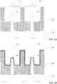
- FIGS. 2A through 2F are cross-sectional views of intermediate stages of a manufacturing method according to some embodiments of the present invention.
- each drawing or bl°Ck in the flowchart diagram represents a pr°Cess ass°Ciated with embodiments of the method described.
- additional bl°Cks and drawings that describe the embodiments may be added.
- the semiconductor structure may include a semiconductor substrate 201, and at least two semiconductor fins on semiconductor substrate 201.
- semiconductor substrate 201 may be a silicon substrate, and a well region (not shown) may be formed in semiconductor substrate 201.
- the at least two semiconductor fins may include a first semiconductor fin 202 and a second semiconductor fin 201.
- the substrate structure may also include an insulating material layer 204 on semiconductor substrate 201. Insulating material layer 204 may include a shallow trench isolation (STI) region and an interlayer dielectric layer.
- STI shallow trench isolation
- insulating material layer 204 has at least two recesses including a first recess 214 and a second recess 224.
- First recess 214 exposes an upper portion of first semiconductor fin 202
- second recess 224 exposes an upper portion of second semiconductor fin 203.
- the opening A of first recess 214 has a lateral surface area greater than a lateral surface area of the opening B of second recess 224.
- the term "the lateral surface area of an opening A) is defined as a surface area of the opening of an recess in a direction parallel to the surface of the substrate.
- an interface layer (not shown) is formed on the exposed portion of the first semiconductor fin 202 and second semiconductor fin 203.
- the interface layer may include s silicon oxide layer.
- a gate dielectric layer is formed on each of the recesses and the exposed portions of the semiconductor fins.
- a gate dielectric layer 205 is formed on the surface of first recess 214 and the corresponding exposed portion of first semiconductor fin 202 and on second recess 224 and on the corresponding exposed portion of second semiconductor fin 203. Further, an annealing pr°Cess may be performed after forming the gate dielectric layer.
- first work function adjustment layer 206 is formed on gate dielectric layer 205, as shown in FIG. 2C .
- first work function adjustment layer 206 may be an n-type work function adjustment layer including, e.g., TiAl, TiCAl, TiNAl, or TiSiAl.
- a functional layer 207 is formed on first work function adjustment layer 206, as shown in FIG. 2D .
- functional layer 207 may be used to adjust the work function of a subsequent formed gate and to serve as a diffusion barrier layer.
- functional layer 207 includes TiN.
- a portion of function layer 207 on first semiconductor fin 202 has a thickness greater than a thickness of a portion of function layer 207 on second semiconductor fin 203.
- forming functional layer 207 on first work function adjustment layer 206 of first recess 214 and of second recess 214 may be performed in one step.
- forming functional layer 207 on first work function adjustment layer 206 of first recess 214 and of second recess 214 may be performed in multiple steps, for example, a first portion of functional layer 207 may be first formed on first work function adjustment layer 206 of first recess 214, and a second portion of functional layer 207 may be then formed on first work function adjustment layer 206 of second recess 224, and vice versa.
- a gate layer 208' is formed on functional layer 207, as shown in FIG. 2E .
- tungsten (W) may be deposited on functional layer 207 as gate layer 208'.
- a planarization e.g., chemical mechanical polishing
- pr°Cess may be formed on gate layer 208' to form gates 208 on the first and second fins, as shown in FIG. 2F .
- different portions of the functional layer have different thicknesses that depend from the lateral surface areas of the openings of the different recesses.
- the thickness of a first portion of the functional layer may be relatively large because of the large amount of residues left in the recess (e.g., first recess) having a relatively larger lateral surface area of the opening when the gate is formed, and thus the thickness of the first portion of the functional layer is relatively large, thereby reducing the diffusion effect of the residue on the device work function.
- the thickness of a second portion of the functional layer may be relatively small because of the small amount of residues left in the recess (e.g., second recess) having a smaller lateral surface area of the opening when the gate is formed, and thus the thickness of the second portion of the functional layer is relatively small, thereby reducing the effect of the functional layer itself on the device work function.
- the channel length is related to the thickness of the functional layer and concluded that different thicknesses of a functional layer may be formed in a device having different channel lengths to minimize the effect of the functional layer on the work function of the device.
- the length of a gate on the first semiconductor fin of the first recess in the longitudinal direction is longer than the length of a gate on the second semiconductor fin of the second recess in the longitudinal direction (i.e., the second channel, also referred to as the short channel). That is, the thickness of the portion of the functional layer in the device having the long channel may be larger than the thickness of the portion of the functional layer in the device having the short channel.
- the length of the gate on the first semiconductor fin of the first recess in the longitudinal direction is in the range between 45 nm and 55 nm, e.g., 50 nm.
- the functional layer on the first semiconductor fin may have a thickness in the range between 20 nm and 40 nm.
- the length of the gate on the second semiconductor fin of the second recess in the longitudinal direction is in the range between 14 nm and 20 nm, e.g., 16 nm.
- the functional layer on the second semiconductor fin may have a thickness in the range between 10 nm and 20 nm.
- the ratio of gate length to the functional layer thickness is in the range between 0.7 and 2.75.
- forming a functional layer having different thicknesses in different recesses may be realized using a plasma enhanced chemical vapor deposition (PECVD) or atomic layer deposition (ALD) pr°Cess.
- PECVD plasma enhanced chemical vapor deposition
- ALD atomic layer deposition
- the following disclosure uses a TiN functional layer as an example to describe the formation of a functional layer using a PECVD pr°Cess.
- step (a) a precursor TiCl 4 and NH 3 is supplied to a reaction chamber, TiN is formed by the reaction of TiCl 4 and NH 3 .
- TiN may be formed by thermal deposition at a temperature in the range between 400 °C and 500 °C .
- step (b) the supply of TiCl 4 and NH 3 is stopped.
- a purge gas is supplied into the reaction chamber for cleaning.
- the purge gas may include an inert gas such as argon.
- the purge gas may include hydrogen. After cleaning, any residue in step (a) may be removed to avoid the effect of residue on subsequent deposition.
- steps (a) and (b) are repeatedly performed until a desired thickness of the functional layer is formed.
- the step coverage of PECVD is close to 80%, the effect of TiN loading by PECVD can be achieved by depositing a thicker TiN layer in a larger lateral surface area of a recess.
- the method may further include step (c) that includes introducing a source gas including a plasma of NH 3 in the reaction chamber.
- steps (a) and (b) may be performed repeatedly 10 times, and step (c) may be performed once after step (b).
- the introduction of the plasma of NH3 as the source gas can increase the N content in the subsequent step (a) and decrease the Cl content.
- the loading effect of PECVD is increased, to improve the deposition of a thicker TiN layer in a recess with a larger lateral surface area of the opening.
- FIG. 3 is a simplified flowchart of a method of manufacturing a semiconductor device according to another embodiment of the present invention.
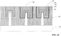
- FIGS. 4A through 4I are cross-sectional views of various stages of a method of manufacturing a semiconductor device according to another embodiment of the present invention. The method of manufacturing a semiconductor device according to another embodiment of the present invention will be described with reference to FIG. 3 and FIGS. 4A through 4I .
- a substrate structure is provided. As shown in FIG. 4A , comparing with the structure of FIG. 2A , the substrate structure of FIG. 3A further includes, in addition to first and second semiconductor fins 202, 203, a third semiconductor fin 301, and in addition to first and second recesses 214, 224, a third recess 302 exposing an upper portion of third semiconductor fin 301.
- a gate dielectric layer is formed on each of the recesses and the exposed surfaces of the corresponding semiconductor fins.
- a gate dielectric layer 205 e.g., a high-k dielectric layer
- first work function adjustment layer 206 is formed on gate dielectric layer 205, as shown in FIG. 4C .
- first work function adjustment layer 206 is a p-type work function adjustment layer.
- the p-type work function adjustment layer may include TiN, TaN, or TaC.
- step 308 a portion of first work function adjustment layer 206 on gate dielectric layer 205 on the surface of first semiconductor fin 202 of first recess 214 and on gate dielectric layer 205 on the surface of second semiconductor fin 203 of second recess 224 is removed, as shown in FIG. 4D .
- a mask layer my be formed on a portion of first work function adjustment layer 206 on gate dielectric layer 205 on the surface of third semiconductor fin 301 of third recess 302, then the portion of first work function adjustment layer 206 not covered by the mask layer is removed.
- a second first work function adjustment layer 206' is formed on a portion of gate dielectric layer 205 on the surface of first semiconductor fin 202 of first recess 214 and a portion of gate dielectric layer 205 on the surface of second semiconductor fin 203 of second recess 224, and on a portion of first work function adjustment layer 206 on the surface of third semiconductor fin 301 of third recess 302, as shown in FIG. 4E .
- a second work function adjustment layer 303 is formed on second first work function adjustment layer 206', as shown in FIG. 4F .
- second work function adjustment layer 303 is an n-type work function adjustment layer including, for example, TiAl, TiCAl, TiNAl, or TiSiAl.
- a functional layer 207 is formed on second work function adjustment layer 303, as shown in FIG. 4G .
- TiN layer may be formed as the functional layer according to the TiN forming pr°Cess described in above sections.
- a gate layer (e.g., tungsten) 208' is formed on functional layer 207, as shown in FIG. 4H .
- a planarization pr°Cess is performed on gate layer 208 to form gates 208 of the semiconductor fins in the recesses, as shown in FIG. 4I .
- embodiments of the present invention provide a semiconductor device and method for manufacturing the same that have different thicknesses of a functional layer in the semiconductor device having different channel lengths to minimize the effect of the functional layer on the work function of the semiconductor device.
Landscapes
- Chemical & Material Sciences (AREA)
- Engineering & Computer Science (AREA)
- Electrodes Of Semiconductors (AREA)
- Insulated Gate Type Field-Effect Transistor (AREA)
- Composite Materials (AREA)
- Materials Engineering (AREA)
- Chemical Kinetics & Catalysis (AREA)
- General Chemical & Material Sciences (AREA)
- Manufacturing & Machinery (AREA)
- Metal-Oxide And Bipolar Metal-Oxide Semiconductor Integrated Circuits (AREA)
Abstract
Description
- This application claims priority to Chinese Application No.
201610620771.X, filed on August 01, 2016 - The present invention relates to semiconductor technology. More particularly, embodiments of the present invention provide a semiconductor device and method of manufacturing the same.
- The work function of an n-type Fin Field Effect Transistor (FinFET) having a tungsten gate is mainly determined by the n-type work function adjustment layer. However, a functional layer is generally disposed between the n-type work function adjustment layer and the gate, and the functional layer typically uses a p-type work function adjustment layer such as TiN. Thus, the presence of the functional layer may adversely affect the work function of the n-type Fin Field Effect Transistor. In this case, it is desirable that the thickness of the functional layer is as small as possible.
- Further, a residue (e.g., F) left in the gate after forming the gate may diffuse into the functional layer and into the n-type work function adjustment layer, which may also adversely affect the work function of the n-type Fin Field Effect Transistor. In this case, it is desirable that the thickness of the functional layer is as large as possible.
- Therefore, the thickness of the functional layer is of particular importance for an n-type Fin Field Effect Transistor.
- It is an object of the present invention to provide a method of manufacturing a semiconductor device and a resulting structure of implementing a semiconductor device by which a greater thickness of the functional layer in a recess region having a larger opening surface than the functional layer in a recess region having a smaller opening surface may be created.
- The object is achieved by the features of the respective independent claims. Further embodiments are defined in the respective dependent claims.
- A first aspect of the present invention provides a method of manufacturing a semiconductor device.
- The method includes providing a semiconductor substrate comprising at least two semiconductor fins having first and second semiconductor fins; forming an insulating layer on the semiconductor substrate, the insulating layer comprising at least two recesses having a first recess exposing an upper portion of the first semiconductor fin and a second recess exposing an upper portion of the second semiconductor fin; forming a gate dielectric layer on the first and second recesses and the exposed upper portions of the first and second semiconductor fins; forming a first work function adjustment layer on the gate dielectric layer; forming a functional layer on the first function adjustment layer; and forming first and second gates on portions of the functional layer of the respective first and second semiconductor fins. The surface area of a lateral opening of the first recess is larger than the surface area of a lateral opening of the second recess, and a thickness of a portion of the functional layer on the first semiconductor fin is greater than a thickness of a portion of the functional layer on the second semiconductor fin.
- Preferably, the first gate of the first semiconductor fin has a length in a longitudinal direction larger than a length of the second gate of the second semiconductor fin in the longitudinal direction.
- Preferably, the length of the first gate is in a range between 45 nm and 55 nm, and the thickness of the portion of the functional layer on the first semiconductor fin is in a range between 20 nm and 40 nm; and the length of the second gate is in a range between 14 nm and 20 nm, and the thickness of the portion of the functional layer on the second semiconductor fin is in a range between 10 nm and 20 nm.
- Preferably, the functional layer is configured to adjust the work function of the first and second gates and configured to be a diffusion barrier layer.
- Preferably, forming the functional layer comprises a plasma enhanced chemical vapor deposition (PECVD) or an atomic layer deposition (ALD) pr°Cess.
- Preferably, the functional layer includes TiN; and the PECVD pr°Cess includes the steps of: (a) introducing a precursor of TiCl4 and NH3 into a reaction chamber to form a TiN layer; (b) stopping introducing the precursor of TiCl4 and NH3 into the reaction chamber; introducing a purge gas into the reaction chamber for cleaning; repeating (a) and (b) until a desired thickness of the functional layer is formed.
- Preferably, the step (a) is performed at a temperature in a range between 400 °C and 500 °C.
- Preferably, the step of repeating (a) and (b) includes at least one iteration, and the method further includes, after performing step (b): step (c): introducing a source gas comprising a plasma NH3 into the reaction chamber.
- Preferably, the purge gas comprises an inert gas.
- Preferably, the at least two semiconductor fins further includes a third semiconductor fin, and the at least two recesses further includes a third recess exposing an upper portion of the third semiconductor fin; the method further includes, after forming the first work function adjustment layer on the gate dielectric layer: removing a portion of the first work function adjustment layer on the gate dielectric layer on the first recess, on the first semiconductor fin, on the second recess and on the second semiconductor fin to expose a portion of the gate dielectric layer on the first recess, on the first semiconductor fin, on the second recess and on the second semiconductor fin; forming a next first work function adjustment layer on the exposed portion of the gate dielectric layer on the first recess, on the first semiconductor fin, on the second recess and on the second semiconductor fin and on a portion of the first work function adjustment layer on the third recess and on the third semiconductor fin; and forming a second work function adjustment layer on the next first work function adjustment layer. Forming the functional layer on the first work function layer includes: forming the functional layer on the second work function adjustment layer.
- Preferably, the first work function adjustment layer is an n-type work function adjustment layer. In one embodiment, the n-type work function adjustment layer comprises TiAl, TiCAl, TiNAl, or TiSiAl.
- Preferably, the first work function adjustment layer is a p-type work function adjustment layer, and the second work function adjustment layer is an n-type work function adjustment layer. In one embodiment, the p-type work function adjustment layer includes TiN, TaN, or TaC; and the n-type work function adjustment layer includes TiAl, TiCAl, TiNAl, or TiSiAl.
- Preferably, the method further includes forming a third gate on the functional layer of the third semiconductor fin.
- Preferably, forming the first, second and third gates comprises: forming a gate layer on the functional layer; and planarizing the gate layer to form the first, second, and third gates.
- A second aspect of the present invention provides a semiconductor device.
- The semiconductor device includes a semiconductor substrate comprising at least two semiconductor fins having first and second semiconductor fins; an insulating layer on the semiconductor substrate, the insulating layer comprising at least two recesses having a first recess exposing an upper portion of the first semiconductor fin and a second recess exposing an upper portion of the second semiconductor fin; a gate dielectric layer on the first and second recesses and the exposed upper portions of the first and second semiconductor fins; a first work function adjustment layer on the gate dielectric layer; a functional layer on the first function adjustment layer; and first and second gates on portions of the functional layer of the respective first and second semiconductor fins. The surface area of a lateral opening of the first recess is larger than the surface area of a lateral opening of the second recess. The thickness of a portion of the functional layer on the first semiconductor fin is greater than the thickness of a portion of the functional layer on the second semiconductor fin.
- Preferably, the first gate of the first semiconductor fin has a length in a longitudinal direction larger than a length of the second gate of the second semiconductor fin in the longitudinal direction.
- Preferably, the at least two semiconductor fins further includes a third semiconductor fin; the at least two recesses further includes a third recess exposing an upper portion of the third semiconductor fin; and a second work function adjustment layer on the first work function adjustment layer. The first work function adjustment layer is a p-type work function adjustment layer, and the second work function adjustment layer is an n-type work function adjustment layer.
- Preferably, the p-type work function adjustment layer comprises TiN, TaN, or TaC; and the n-type work function adjustment layer comprises TiAl, TiCAl, TiNAl, or TiSiAl.
- A semiconductor device according to the second aspect of the present invention may be obtained by a method according to the first aspect of the present invention.
- The following description, together with the accompanying drawings, will provide a better understanding of the nature and advantages of the claimed invention.
- The accompanying drawings, referred to herein and constituting a part hereof, illustrate embodiments of the invention. The drawings together with the description serve to explain the principles of the invention.
-
FIG. 1 is a flowchart illustrating a method for manufacturing of a semiconductor device according to one embodiment of the present invention. -
FIG. 2A is a cross-sectional view of an intermediate stage of a manufacturing method according to some embodiments of the present invention. -
FIG. 2B is a cross-sectional view of an intermediate stage of a manufacturing method according to some embodiments of the present invention. -
FIG. 2C is a cross-sectional view of an intermediate stage of a manufacturing method according to some embodiments of the present invention. -
FIG. 2D is a cross-sectional view of an intermediate stage of a manufacturing method according to some embodiments of the present invention. -
FIG. 2E is a cross-sectional view of an intermediate stage of a manufacturing method according to some embodiments of the present invention. -
FIG. 2F is a cross-sectional view of an intermediate stage of a manufacturing method according to some embodiments of the present invention. -
FIG. 3 is a flowchart illustrating a method for manufacturing of a semiconductor device according to another embodiment of the present invention. -
FIG. 4A is a cross-sectional view of an intermediate stage of a manufacturing method according to some embodiments of the present invention. -
FIG. 4B is a cross-sectional view of an intermediate stage of a manufacturing method according to some embodiments of the present invention. -
FIG. 4C is a cross-sectional view of an intermediate stage of a manufacturing method according to some embodiments of the present invention. -
FIG. 4D is a cross-sectional view of an intermediate stage of a manufacturing method according to some embodiments of the present invention. -
FIG. 4E is a cross-sectional view of an intermediate stage of a manufacturing method according to some embodiments of the present invention. -
FIG. 4F is a cross-sectional view of an intermediate stage of a manufacturing method according to some embodiments of the present invention. -
FIG. 4G is a cross-sectional view of an intermediate stage of a manufacturing method according to some embodiments of the present invention. -
FIG. 4H is a cross-sectional view of an intermediate stage of a manufacturing method according to some embodiments of the present invention. -
FIG. 4I is a cross-sectional view of an intermediate stage of a manufacturing method according to some embodiments of the present invention. - In the following description, numerous specific details are provided for a thorough understanding of the present invention. However, it should be appreciated by those of skill in the art that the present invention may be realized without one or more of these details. In other examples, features and techniques known in the art will not be described for purposes of brevity.
- It should be understood that the drawings are not drawn to scale, and similar reference numbers are used for representing similar elements. Embodiments of the invention are described herein with reference to perspective cross-section illustrations that are schematic illustrations of idealized embodiments (and intermediate structures) of the invention. The thickness of layers and regions in the drawings may be exaggerated relative to each other for clarity. Additionally, variations from the shapes of the illustrations as a result, for example, of manufacturing techniques and/or tolerances, are to be expected. Thus, embodiments of the invention should not be construed as limited to the particular shapes of regions illustrated herein but are to include deviations in shapes that result, for example, from manufacturing.
- It will be understood that, when an element or layer is referred to as "on," "disposed on," "adjacent to," "connected to," or "coupled to" another element or layer, it can be disposed directly on the other element or layer, adjacent to, connected or coupled to the other element or layer, or intervening elements or layers may also be present. In contrast, when an element is referred to as being "directly on," directly disposed on," "directly connected to," or "directly coupled to" another element or layer, there are no intervening elements or layers present between them. It will be understood that, although the terms "first," "second," "third," etc. may be used herein to describe various elements, components, regions, layers and/or sections, these elements, components, regions, layers and/or sections should not be limited by these terms. These terms are only used to distinguish one element, component, region, layer or section from another region, layer or section. Thus, a first element, component, region, layer or section discussed below could be termed a second element, component, region, layer or section without departing from the teachings of the present invention.
- The use of the terms first, second, third, etc. do not denote any order, but rather the terms first, second, third, etc. are used to distinguish one element from another. Furthermore, the use of the terms a, an, etc. does not denote a limitation of quantity, but rather denote the presence of at least one of the referenced items.
- The term "substrate" may include any structure having an exposed surface with which to form an integrated circuit. The term "substrate" is understood to include semiconductor wafers and is also used to refer to semiconductor structures during pr°Cessing and may include other layers that have been fabricated thereupon. A "substrate" may include doped and undoped semiconductor wafers, epitaxial semiconductor layers, as well as other semiconductor structures.
- As described in the background section, when the silicide layers of adjacent source regions are joined together, the surface area of the joined silicide layers is relatively small and the contact resistance is high, or when the silicide layers of adjacent source regions are not joined together, the volume of the epitaxial silicide layers is relatively small, the surface of the contact element has a polygonal shape, the surface area of the contact element is small, and the contact element has a high resistance. Thus, the present inventor provide a method for manufacturing a semiconductor device that can provide a large volume and a large surface area of the source or drain region to reduce the contact resistance.
- In accordance with some embodiments of the present invention,
FIG. 1 is a flowchart diagram illustrating a manufacturing method according to one embodiment of the present invention.FIGS. 2A through 2F are cross-sectional views of intermediate stages of a manufacturing method according to some embodiments of the present invention. In the disclosure, each drawing or bl°Ck in the flowchart diagram represents a pr°Cess ass°Ciated with embodiments of the method described. Those of skill in the art will recognize that additional bl°Cks and drawings that describe the embodiments may be added. - Referring to
FIG. 1 , instep 102, a semiconductor structure is provided. As shown inFIG. 2A , the semiconductor structure may include asemiconductor substrate 201, and at least two semiconductor fins onsemiconductor substrate 201. In one embodiment,semiconductor substrate 201 may be a silicon substrate, and a well region (not shown) may be formed insemiconductor substrate 201. The at least two semiconductor fins may include afirst semiconductor fin 202 and asecond semiconductor fin 201. The substrate structure may also include an insulatingmaterial layer 204 onsemiconductor substrate 201. Insulatingmaterial layer 204 may include a shallow trench isolation (STI) region and an interlayer dielectric layer. Referring toFIG. 2A , insulatingmaterial layer 204 has at least two recesses including afirst recess 214 and asecond recess 224.First recess 214 exposes an upper portion offirst semiconductor fin 202, andsecond recess 224 exposes an upper portion ofsecond semiconductor fin 203. The opening A offirst recess 214 has a lateral surface area greater than a lateral surface area of the opening B ofsecond recess 224. As used herein, the term "the lateral surface area of an opening A) is defined as a surface area of the opening of an recess in a direction parallel to the surface of the substrate. Further, in one embodiment, an interface layer (not shown) is formed on the exposed portion of thefirst semiconductor fin 202 andsecond semiconductor fin 203. The interface layer may include s silicon oxide layer. - Next, in
step 104, a gate dielectric layer is formed on each of the recesses and the exposed portions of the semiconductor fins. As shown inFIG. 2B , agate dielectric layer 205 is formed on the surface offirst recess 214 and the corresponding exposed portion offirst semiconductor fin 202 and onsecond recess 224 and on the corresponding exposed portion ofsecond semiconductor fin 203. Further, an annealing pr°Cess may be performed after forming the gate dielectric layer. - Next, in
step 106, a first workfunction adjustment layer 206 is formed ongate dielectric layer 205, as shown inFIG. 2C . In one embodiment, first workfunction adjustment layer 206 may be an n-type work function adjustment layer including, e.g., TiAl, TiCAl, TiNAl, or TiSiAl. - Next, in
step 108, afunctional layer 207 is formed on first workfunction adjustment layer 206, as shown inFIG. 2D . In one embodiment,functional layer 207 may be used to adjust the work function of a subsequent formed gate and to serve as a diffusion barrier layer. In an example embodiment,functional layer 207 includes TiN. A portion offunction layer 207 onfirst semiconductor fin 202 has a thickness greater than a thickness of a portion offunction layer 207 onsecond semiconductor fin 203. In one embodiment, formingfunctional layer 207 on first workfunction adjustment layer 206 offirst recess 214 and ofsecond recess 214 may be performed in one step. In another embodiment, formingfunctional layer 207 on first workfunction adjustment layer 206 offirst recess 214 and ofsecond recess 214 may be performed in multiple steps, for example, a first portion offunctional layer 207 may be first formed on first workfunction adjustment layer 206 offirst recess 214, and a second portion offunctional layer 207 may be then formed on first workfunction adjustment layer 206 ofsecond recess 224, and vice versa. - Next, in
step 110, a gate layer 208' is formed onfunctional layer 207, as shown inFIG. 2E . In an example embodiment, tungsten (W) may be deposited onfunctional layer 207 as gate layer 208'. - Further, after forming gate layer 208', a planarization (e.g., chemical mechanical polishing) pr°Cess may be formed on gate layer 208' to form
gates 208 on the first and second fins, as shown inFIG. 2F . - In the method for manufacturing a semiconductor device according to one embodiment of the present invention, different portions of the functional layer have different thicknesses that depend from the lateral surface areas of the openings of the different recesses. The thickness of a first portion of the functional layer may be relatively large because of the large amount of residues left in the recess (e.g., first recess) having a relatively larger lateral surface area of the opening when the gate is formed, and thus the thickness of the first portion of the functional layer is relatively large, thereby reducing the diffusion effect of the residue on the device work function. The thickness of a second portion of the functional layer may be relatively small because of the small amount of residues left in the recess (e.g., second recess) having a smaller lateral surface area of the opening when the gate is formed, and thus the thickness of the second portion of the functional layer is relatively small, thereby reducing the effect of the functional layer itself on the device work function.
- The present inventor discovered that the channel length is related to the thickness of the functional layer and concluded that different thicknesses of a functional layer may be formed in a device having different channel lengths to minimize the effect of the functional layer on the work function of the device.
- In one embodiment, the length of a gate on the first semiconductor fin of the first recess in the longitudinal direction (i.e., the first channel, also referred to as the long channel) is longer than the length of a gate on the second semiconductor fin of the second recess in the longitudinal direction (i.e., the second channel, also referred to as the short channel). That is, the thickness of the portion of the functional layer in the device having the long channel may be larger than the thickness of the portion of the functional layer in the device having the short channel. In a preferred embodiment, the length of the gate on the first semiconductor fin of the first recess in the longitudinal direction is in the range between 45 nm and 55 nm, e.g., 50 nm. The functional layer on the first semiconductor fin may have a thickness in the range between 20 nm and 40 nm. The length of the gate on the second semiconductor fin of the second recess in the longitudinal direction is in the range between 14 nm and 20 nm, e.g., 16 nm. The functional layer on the second semiconductor fin may have a thickness in the range between 10 nm and 20 nm. As described above, the present inventor discovered that the gate length and the functional layer thickness dependent from each other. In some embodiments, the ratio of gate length to the functional layer thickness is in the range between 0.7 and 2.75. By maintaining a ratio range between the channel length and the functional layer thickness, the effect of the functional layer on the work function of the semiconductor device can be reduced.
- In one embodiment, forming a functional layer having different thicknesses in different recesses may be realized using a plasma enhanced chemical vapor deposition (PECVD) or atomic layer deposition (ALD) pr°Cess.
- The following disclosure uses a TiN functional layer as an example to describe the formation of a functional layer using a PECVD pr°Cess.
- First, in step (a), a precursor TiCl4 and NH3 is supplied to a reaction chamber, TiN is formed by the reaction of TiCl4 and NH3. For example, TiN may be formed by thermal deposition at a temperature in the range between 400 °C and 500 °C.
- Next, in step (b), the supply of TiCl4 and NH3 is stopped. A purge gas is supplied into the reaction chamber for cleaning. The purge gas may include an inert gas such as argon. Alternatively, the purge gas may include hydrogen. After cleaning, any residue in step (a) may be removed to avoid the effect of residue on subsequent deposition.
- Thereafter, steps (a) and (b) are repeatedly performed until a desired thickness of the functional layer is formed. The step coverage of PECVD is close to 80%, the effect of TiN loading by PECVD can be achieved by depositing a thicker TiN layer in a larger lateral surface area of a recess.
- Preferably, at least one iteration of steps (a) and (b) will be repeated. After performing step (b), the method may further include step (c) that includes introducing a source gas including a plasma of NH3 in the reaction chamber. For example, steps (a) and (b) may be performed repeatedly 10 times, and step (c) may be performed once after step (b). The present inventor discovered that, in the pr°Cess of forming TiN using the PECVD technique, the introduction of the plasma of NH3 as the source gas can increase the N content in the subsequent step (a) and decrease the Cl content. That enables the increase of the thickness of the functional layer deposited in the first recess having a large lateral opening area more than the thickness of the thickness of the functional layer deposited in the second recess having a smaller lateral opening area, i.e., the loading effect of PECVD is increased, to improve the deposition of a thicker TiN layer in a recess with a larger lateral surface area of the opening.
-
FIG. 3 is a simplified flowchart of a method of manufacturing a semiconductor device according to another embodiment of the present invention.FIGS. 4A through 4I are cross-sectional views of various stages of a method of manufacturing a semiconductor device according to another embodiment of the present invention. The method of manufacturing a semiconductor device according to another embodiment of the present invention will be described with reference toFIG. 3 andFIGS. 4A through 4I . - Referring to
FIG. 3 , instep 302, a substrate structure is provided. As shown inFIG. 4A , comparing with the structure ofFIG. 2A , the substrate structure ofFIG. 3A further includes, in addition to first andsecond semiconductor fins third semiconductor fin 301, and in addition to first andsecond recesses third recess 302 exposing an upper portion ofthird semiconductor fin 301. - Next, in
step 304, a gate dielectric layer is formed on each of the recesses and the exposed surfaces of the corresponding semiconductor fins. As shown inFIG. 4B , a gate dielectric layer 205 (e.g., a high-k dielectric layer) is formed on the surface offirst recess 214 and correspondingfirst semiconductor fin 202, on the surface ofsecond recess 224 and correspondingsecond semiconductor fin 203, and on the surface ofthird recess 302 and correspondingthird semiconductor fin 301. - Thereafter, in
step 306, a first workfunction adjustment layer 206 is formed ongate dielectric layer 205, as shown inFIG. 4C . In one embodiment, first workfunction adjustment layer 206 is a p-type work function adjustment layer. In an exemplary embodiment, the p-type work function adjustment layer may include TiN, TaN, or TaC. - Next, in
step 308, a portion of first workfunction adjustment layer 206 ongate dielectric layer 205 on the surface offirst semiconductor fin 202 offirst recess 214 and ongate dielectric layer 205 on the surface ofsecond semiconductor fin 203 ofsecond recess 224 is removed, as shown inFIG. 4D . For example, a mask layer my be formed on a portion of first workfunction adjustment layer 206 ongate dielectric layer 205 on the surface ofthird semiconductor fin 301 ofthird recess 302, then the portion of first workfunction adjustment layer 206 not covered by the mask layer is removed. - Next, in
step 310, a second first work function adjustment layer 206' is formed on a portion ofgate dielectric layer 205 on the surface offirst semiconductor fin 202 offirst recess 214 and a portion ofgate dielectric layer 205 on the surface ofsecond semiconductor fin 203 ofsecond recess 224, and on a portion of first workfunction adjustment layer 206 on the surface ofthird semiconductor fin 301 ofthird recess 302, as shown inFIG. 4E . - Next, in
step 312, a second workfunction adjustment layer 303 is formed on second first work function adjustment layer 206', as shown inFIG. 4F . In one embodiment, second workfunction adjustment layer 303 is an n-type work function adjustment layer including, for example, TiAl, TiCAl, TiNAl, or TiSiAl. - Next, in
step 314, afunctional layer 207 is formed on second workfunction adjustment layer 303, as shown inFIG. 4G . TiN layer may be formed as the functional layer according to the TiN forming pr°Cess described in above sections. - Thereafter, a gate layer (e.g., tungsten) 208' is formed on
functional layer 207, as shown inFIG. 4H . - Thereafter, a planarization pr°Cess is performed on
gate layer 208 to formgates 208 of the semiconductor fins in the recesses, as shown inFIG. 4I . - Thus, embodiments of the present invention provide a semiconductor device and method for manufacturing the same that have different thicknesses of a functional layer in the semiconductor device having different channel lengths to minimize the effect of the functional layer on the work function of the semiconductor device.
- °C [0081] Finally, some of the features of the preferred embodiments of the present invention could be used to advantage without the corresponding use of other features. As such, the foregoing description should be considered as merely illustrative of the principles of the invention, and not in limitation thereof.
Claims (15)
- A method of manufacturing a semiconductor device, the method comprising:providing a semiconductor substrate comprising at least two semiconductor fins having first and second semiconductor fins;forming an insulating layer on the semiconductor substrate, the insulating layer comprising at least two recesses having a first recess exposing an upper portion of the first semiconductor fin and a second recess exposing an upper portion of the second semiconductor fin;forming a gate dielectric layer on the first and second recesses and the exposed upper portions of the first and second semiconductor fins;forming a first work function adjustment layer on the gate dielectric layer;forming a functional layer on the first function adjustment layer; andforming first and second gates on portions of the functional layer of the respective first and second semiconductor fins,wherein a surface area of a lateral opening of the first recess is larger than a surface area of a lateral opening of the second recess, and a thickness of a portion of the functional layer on the first semiconductor fin is greater than a thickness of a portion of the functional layer on the second semiconductor fin.
- The method of claim 1, wherein the first gate of the first semiconductor fin has a length in a longitudinal direction larger than a length of the second gate of the second semiconductor fin in the longitudinal direction; and
wherein preferably: the length of the first gate is in a range between 45 nm and 55 nm, and the thickness of the portion of the functional layer on the first semiconductor fin is in a range between 20 nm and 40 nm; and the length of the second gate is in a range between 14 nm and 20 nm, and the thickness of the portion of the functional layer on the second semiconductor fin is in a range between 10 nm and 20 nm. - The method of claim 1 or 2, wherein the functional layer is configured to adjust the work function of the first and second gates and configured to be a diffusion barrier layer.
- The method of anyone of the claims 1-3, wherein forming the functional layer comprises a plasma enhanced chemical vapor deposition (PECVD) or an atomic layer deposition (ALD) pr°Cess.
- The method of claim 4, wherein the functional layer comprises TiN; and the PECVD pr°Cess comprises:(a) introducing a precursor of TiCl4 and NH3 into a reaction chamber to form a TiN layer;(b) stopping introducing the precursor of TiCl4 and NH3 into the reaction chamber; introducing a purge gas into the reaction chamber for cleaning;repeating (a) and (b) until a desired thickness of the functional layer is formed.
- The method of claim 5, wherein at least one of:(a) is performed at a temperature in a range between 400 °C and 500 °C;repeating (a) and (b) comprises at least one iteration, and the method further comprises, after performing (b), (c) introducing a source gas comprising a plasma NH3 into the reaction chamber; and
the purge gas comprises an inert gas. - The method of anyone of the claims 1-6, wherein the at least two semiconductor fins further comprises a third semiconductor fin, and the at least two recesses further comprises a third recess exposing an upper portion of the third semiconductor fin; the method further comprising, after forming the first work function adjustment layer on the gate dielectric layer:removing a portion of the first work function adjustment layer on the gate dielectric layer on the first recess, on the first semiconductor fin, on the second recess and on the second semiconductor fin to expose a portion of the gate dielectric layer on the first recess, on the first semiconductor fin, on the second recess and on the second semiconductor fin;forming a next first work function adjustment layer on the exposed portion of the gate dielectric layer on the first recess, on the first semiconductor fin, on the second recess and on the second semiconductor fin and on a portion of the first work function adjustment layer on the third recess and on the third semiconductor fin;forming a second work function adjustment layer on the next first work function adjustment layer;wherein forming the functional layer on the first work function layer comprises:forming the functional layer on the second work function adjustment layer.
- The method of anyone of the claims 1-7, wherein the first work function adjustment layer is an n-type work function adjustment layer; and
wherein preferably: the n-type work function adjustment layer comprises TiAl, TiCAl, TiNAl, or TiSiAl. - The method of claim 7, wherein the first work function adjustment layer is a p-type work function adjustment layer, and the second work function adjustment layer is an n-type work function adjustment layer; and
wherein preferably: the p-type work function adjustment layer comprises TiN, TaN, or TaC; and the n-type work function adjustment layer comprises TiAl, TiCAl, TiNAl, or TiSiAl. - The method of claim 7, further comprising forming a third gate on the functional layer of the third semiconductor fin.
- The method of claim 10, wherein forming the first, second and third gates comprises:forming a gate layer on the functional layer; andplanarizing the gate layer to form the first, second, and third gates.
- A semiconductor device comprising:a semiconductor substrate comprising at least two semiconductor fins having first and second semiconductor fins;an insulating layer on the semiconductor substrate, the insulating layer comprising at least two recesses having a first recess exposing an upper portion of the first semiconductor fin and a second recess exposing an upper portion of the second semiconductor fin;a gate dielectric layer on the first and second recesses and the exposed upper portions of the first and second semiconductor fins;a first work function adjustment layer on the gate dielectric layer;a functional layer on the first function adjustment layer; andfirst and second gates on portions of the functional layer of the respective first and second semiconductor fins,wherein a surface area of a lateral opening of the first recess is larger than a surface area of a lateral opening of the second recess, and a thickness of a portion of the functional layer on the first semiconductor fin is greater than a thickness of a portion of the functional layer on the second semiconductor fin.
- The semiconductor device of claim 12, wherein the first gate of the first semiconductor fin has a length in a longitudinal direction larger than a length of the second gate of the second semiconductor fin in the longitudinal direction.
- The semiconductor device of claim 12 or 13, wherein:the at least two semiconductor fins further comprises a third semiconductor fin;the at least two recesses further comprises a third recess exposing an upper portion of the third semiconductor fin; the method further comprising, after forming the first work function adjustment layer on the gate dielectric layer;a second work function adjustment layer on the first work function adjustment layer,wherein the first work function adjustment layer is a p-type work function adjustment layer, and the second work function adjustment layer is an n-type work function adjustment layer.
- The semiconductor device of claim 14, wherein:the p-type work function adjustment layer comprises TiN, TaN, or TaC; andthe n-type work function adjustment layer comprises TiAl, TiCAl, TiNAl, or TiSiAl.
Applications Claiming Priority (1)
| Application Number | Priority Date | Filing Date | Title |
|---|---|---|---|
| CN201610620771.XA CN107680938B (en) | 2016-08-01 | 2016-08-01 | Manufacturing method of semiconductor device |
Publications (1)
| Publication Number | Publication Date |
|---|---|
| EP3279933A1 true EP3279933A1 (en) | 2018-02-07 |
Family
ID=59501280
Family Applications (1)
| Application Number | Title | Priority Date | Filing Date |
|---|---|---|---|
| EP17183769.3A Withdrawn EP3279933A1 (en) | 2016-08-01 | 2017-07-28 | Increasing thickness of functional layer according to increasing recess area |
Country Status (3)
| Country | Link |
|---|---|
| US (2) | US10388655B2 (en) |
| EP (1) | EP3279933A1 (en) |
| CN (1) | CN107680938B (en) |
Families Citing this family (6)
| Publication number | Priority date | Publication date | Assignee | Title |
|---|---|---|---|---|
| CN107680938B (en) | 2016-08-01 | 2021-05-28 | 中芯国际集成电路制造(上海)有限公司 | Manufacturing method of semiconductor device |
| US10446686B2 (en) * | 2018-03-09 | 2019-10-15 | International Business Machines Corporation | Asymmetric dual gate fully depleted transistor |
| CN110571193B (en) * | 2018-06-05 | 2021-07-30 | 中芯国际集成电路制造(上海)有限公司 | Manufacturing method of single diffusion blocking structure and manufacturing method of semiconductor device |
| US11018234B2 (en) | 2018-07-26 | 2021-05-25 | Taiwan Semiconductor Manufacturing Co., Ltd. | Semiconductor device and manufacturing method thereof |
| DE102019121270B4 (en) * | 2018-09-28 | 2024-05-08 | Taiwan Semiconductor Manufacturing Co., Ltd. | Formation method of a semiconductor device with fin structures |
| US12230632B2 (en) * | 2020-09-18 | 2025-02-18 | Taiwan Semiconductor Manufacturing Co., Ltd. | Integrated circuit layout and method thereof |
Citations (7)
| Publication number | Priority date | Publication date | Assignee | Title |
|---|---|---|---|---|
| US20100081262A1 (en) * | 2008-09-26 | 2010-04-01 | Taiwan Semiconductor Manufacturing Company, Ltd. | Method for forming metal gates in a gate last process |
| US20130313648A1 (en) * | 2012-05-25 | 2013-11-28 | Wen-Tai Chiang | Semiconductor device having metal gate and manufacturing method thereof |
| US20140374840A1 (en) * | 2013-06-24 | 2014-12-25 | Hye-Lan Lee | Semiconductor devices using mos transistors with nonuniform gate electrode structures and methods of fabricating the same |
| WO2015047313A1 (en) * | 2013-09-27 | 2015-04-02 | Intel Corporation | Non-planar i/o and logic semiconductor devices having different workfunction on common substrate |
| CN104716171A (en) * | 2013-12-11 | 2015-06-17 | 中国科学院微电子研究所 | Semiconductor device and manufacturing method thereof |
| US20150243658A1 (en) * | 2014-02-25 | 2015-08-27 | Globalfoundries Inc. | Integrated circuits with varying gate structures and fabrication methods |
| US9305923B1 (en) * | 2014-12-02 | 2016-04-05 | International Business Machines Corporation | Low resistance replacement metal gate structure |
Family Cites Families (21)
| Publication number | Priority date | Publication date | Assignee | Title |
|---|---|---|---|---|
| KR0147626B1 (en) * | 1995-03-30 | 1998-11-02 | 김광호 | Method for forming gate electrode |
| US20130187236A1 (en) * | 2012-01-20 | 2013-07-25 | Globalfoundries Inc. | Methods of Forming Replacement Gate Structures for Semiconductor Devices |
| CN103531538B (en) * | 2012-07-02 | 2016-01-06 | 中芯国际集成电路制造(上海)有限公司 | The formation method of CMOS (Complementary Metal Oxide Semiconductor) pipe |
| CN103545190B (en) * | 2012-07-16 | 2016-05-04 | 中国科学院微电子研究所 | Method for forming gate structure, method for forming semiconductor device, and semiconductor device |
| CN103871888B (en) * | 2012-12-18 | 2017-09-29 | 中芯国际集成电路制造(上海)有限公司 | Semiconductor devices and forming method thereof |
| CN104282540B (en) * | 2013-07-03 | 2017-09-22 | 中芯国际集成电路制造(上海)有限公司 | Transistor and forming method thereof |
| US9117930B2 (en) * | 2013-08-06 | 2015-08-25 | Globalfoundries Inc. | Methods of forming stressed fin channel structures for FinFET semiconductor devices |
| CN103904028A (en) * | 2013-11-14 | 2014-07-02 | 唐棕 | Semiconductor structure and manufacturing method thereof |
| CN104766823A (en) * | 2014-01-07 | 2015-07-08 | 中国科学院微电子研究所 | Semiconductor device manufacturing method |
| US9431296B2 (en) * | 2014-06-26 | 2016-08-30 | International Business Machines Corporation | Structure and method to form liner silicide with improved contact resistance and reliablity |
| CN105244265B (en) * | 2014-07-09 | 2018-07-20 | 中芯国际集成电路制造(上海)有限公司 | A kind of semiconductor devices and preparation method thereof and electronic device |
| US9330938B2 (en) * | 2014-07-24 | 2016-05-03 | International Business Machines Corporation | Method of patterning dopant films in high-k dielectrics in a soft mask integration scheme |
| US9793269B2 (en) * | 2014-08-07 | 2017-10-17 | Taiwan Semiconductor Manufacturing Company, Ltd. | Semiconductor device and method of manufacture |
| US9337045B2 (en) * | 2014-08-13 | 2016-05-10 | Globalfoundries Inc. | Methods of forming a semiconductor circuit element and semiconductor circuit element |
| CN105514105B (en) * | 2014-09-26 | 2019-08-06 | 联华电子股份有限公司 | Integrated circuit and forming method thereof |
| KR102235612B1 (en) * | 2015-01-29 | 2021-04-02 | 삼성전자주식회사 | Semiconductor device having work-function metal and method of forming the same |
| US9768276B2 (en) * | 2015-04-23 | 2017-09-19 | International Business Machines Corporation | Method and structure of forming FinFET electrical fuse structure |
| US9559205B2 (en) * | 2015-05-29 | 2017-01-31 | Taiwan Semiconductor Manufacturing Company, Ltd. | Structure and formation method of semiconductor device structure |
| US9553092B2 (en) * | 2015-06-12 | 2017-01-24 | Globalfoundries Inc. | Alternative threshold voltage scheme via direct metal gate patterning for high performance CMOS FinFETs |
| KR20170079174A (en) * | 2015-12-30 | 2017-07-10 | 삼성전자주식회사 | Semiconductor device and method for manufacturing the same |
| CN107680938B (en) | 2016-08-01 | 2021-05-28 | 中芯国际集成电路制造(上海)有限公司 | Manufacturing method of semiconductor device |
-
2016
- 2016-08-01 CN CN201610620771.XA patent/CN107680938B/en active Active
-
2017
- 2017-03-29 US US15/473,318 patent/US10388655B2/en active Active
- 2017-07-28 EP EP17183769.3A patent/EP3279933A1/en not_active Withdrawn
-
2019
- 2019-07-03 US US16/503,259 patent/US11145652B2/en active Active
Patent Citations (7)
| Publication number | Priority date | Publication date | Assignee | Title |
|---|---|---|---|---|
| US20100081262A1 (en) * | 2008-09-26 | 2010-04-01 | Taiwan Semiconductor Manufacturing Company, Ltd. | Method for forming metal gates in a gate last process |
| US20130313648A1 (en) * | 2012-05-25 | 2013-11-28 | Wen-Tai Chiang | Semiconductor device having metal gate and manufacturing method thereof |
| US20140374840A1 (en) * | 2013-06-24 | 2014-12-25 | Hye-Lan Lee | Semiconductor devices using mos transistors with nonuniform gate electrode structures and methods of fabricating the same |
| WO2015047313A1 (en) * | 2013-09-27 | 2015-04-02 | Intel Corporation | Non-planar i/o and logic semiconductor devices having different workfunction on common substrate |
| CN104716171A (en) * | 2013-12-11 | 2015-06-17 | 中国科学院微电子研究所 | Semiconductor device and manufacturing method thereof |
| US20150243658A1 (en) * | 2014-02-25 | 2015-08-27 | Globalfoundries Inc. | Integrated circuits with varying gate structures and fabrication methods |
| US9305923B1 (en) * | 2014-12-02 | 2016-04-05 | International Business Machines Corporation | Low resistance replacement metal gate structure |
Also Published As
| Publication number | Publication date |
|---|---|
| US20180033790A1 (en) | 2018-02-01 |
| US11145652B2 (en) | 2021-10-12 |
| US20190326291A1 (en) | 2019-10-24 |
| CN107680938B (en) | 2021-05-28 |
| CN107680938A (en) | 2018-02-09 |
| US10388655B2 (en) | 2019-08-20 |
Similar Documents
| Publication | Publication Date | Title |
|---|---|---|
| US11145652B2 (en) | Increasing thickness of functional layer according to increasing recess area | |
| US11367782B2 (en) | Semiconductor manufacturing | |
| CN110931431A (en) | Semiconductor device and method of manufacturing semiconductor device | |
| US20130001555A1 (en) | Semiconductor structure and method for manufacturing the same | |
| CN112447522A (en) | Method for manufacturing semiconductor device | |
| KR20090019693A (en) | Strained semiconductor device and manufacturing method thereof | |
| WO2013159414A1 (en) | Dual metal gate cmos device and fabrication method thereof | |
| US20250364403A1 (en) | Field effect transistor with source/drain via and method | |
| TW202234587A (en) | Semiconductor device and method for fabricating the same | |
| US20220262928A1 (en) | Device Providing Multiple Threshold Voltages And Methods Of Making The Same | |
| US20120238088A1 (en) | Fabrication method of metal gates for gate-last process | |
| CN114975275A (en) | Semiconductor device and method | |
| US20250366096A1 (en) | Method of forming cfet device by interposer layer replacement and related structures | |
| US8471341B2 (en) | Semiconductor device and method for fabricating the same | |
| CN118099097B (en) | Manufacturing method of semiconductor device | |
| CN106328529B (en) | MOS transistor and method of forming the same | |
| TWI809447B (en) | Semiconductor structure and method for forming thereof | |
| CN116631947A (en) | Semiconductor device and method of forming the same | |
| CN104979289B (en) | A kind of semiconductor devices and preparation method thereof | |
| US12439642B2 (en) | Seam-top seal for dielectrics | |
| TWI854525B (en) | Semiconductor device, fabrication method of the same, and method of forming continuous metal cap over metal gate structure | |
| TWI892570B (en) | Semiconductor device and methods of forming same | |
| TWI908053B (en) | Semiconductor devices and methods for fabricating the same | |
| US20250151326A1 (en) | Method of forming nanostructure device by interposer layer replacement and related structures | |
| US20240395813A1 (en) | Field effect transistor with isolation structure and related method |
Legal Events
| Date | Code | Title | Description |
|---|---|---|---|
| PUAI | Public reference made under article 153(3) epc to a published international application that has entered the european phase |
Free format text: ORIGINAL CODE: 0009012 |
|
| STAA | Information on the status of an ep patent application or granted ep patent |
Free format text: STATUS: THE APPLICATION HAS BEEN PUBLISHED |
|
| AK | Designated contracting states |
Kind code of ref document: A1 Designated state(s): AL AT BE BG CH CY CZ DE DK EE ES FI FR GB GR HR HU IE IS IT LI LT LU LV MC MK MT NL NO PL PT RO RS SE SI SK SM TR |
|
| AX | Request for extension of the european patent |
Extension state: BA ME |
|
| STAA | Information on the status of an ep patent application or granted ep patent |
Free format text: STATUS: REQUEST FOR EXAMINATION WAS MADE |
|
| 17P | Request for examination filed |
Effective date: 20180326 |
|
| RBV | Designated contracting states (corrected) |
Designated state(s): AL AT BE BG CH CY CZ DE DK EE ES FI FR GB GR HR HU IE IS IT LI LT LU LV MC MK MT NL NO PL PT RO RS SE SI SK SM TR |
|
| RAP1 | Party data changed (applicant data changed or rights of an application transferred) |
Owner name: SEMICONDUCTOR MANUFACTURING INTERNATIONAL (SHANGHA Owner name: SEMICONDUCTOR MANUFACTURING INTERNATIONAL (BEIJING |
|
| STAA | Information on the status of an ep patent application or granted ep patent |
Free format text: STATUS: EXAMINATION IS IN PROGRESS |
|
| 17Q | First examination report despatched |
Effective date: 20200608 |
|
| STAA | Information on the status of an ep patent application or granted ep patent |
Free format text: STATUS: THE APPLICATION IS DEEMED TO BE WITHDRAWN |
|
| 18D | Application deemed to be withdrawn |
Effective date: 20201020 |