EP3275955B1 - Electric/electronic part and bonding method - Google Patents
Electric/electronic part and bonding method Download PDFInfo
- Publication number
- EP3275955B1 EP3275955B1 EP16754994.8A EP16754994A EP3275955B1 EP 3275955 B1 EP3275955 B1 EP 3275955B1 EP 16754994 A EP16754994 A EP 16754994A EP 3275955 B1 EP3275955 B1 EP 3275955B1
- Authority
- EP
- European Patent Office
- Prior art keywords
- group
- electric
- composition
- sio
- electronic part
- Prior art date
- Legal status (The legal status is an assumption and is not a legal conclusion. Google has not performed a legal analysis and makes no representation as to the accuracy of the status listed.)
- Active
Links
Images
Classifications
-
- C—CHEMISTRY; METALLURGY
- C09—DYES; PAINTS; POLISHES; NATURAL RESINS; ADHESIVES; COMPOSITIONS NOT OTHERWISE PROVIDED FOR; APPLICATIONS OF MATERIALS NOT OTHERWISE PROVIDED FOR
- C09D—COATING COMPOSITIONS, e.g. PAINTS, VARNISHES OR LACQUERS; FILLING PASTES; CHEMICAL PAINT OR INK REMOVERS; INKS; CORRECTING FLUIDS; WOODSTAINS; PASTES OR SOLIDS FOR COLOURING OR PRINTING; USE OF MATERIALS THEREFOR
- C09D183/00—Coating compositions based on macromolecular compounds obtained by reactions forming in the main chain of the macromolecule a linkage containing silicon, with or without sulfur, nitrogen, oxygen, or carbon only; Coating compositions based on derivatives of such polymers
- C09D183/10—Block or graft copolymers containing polysiloxane sequences
-
- C—CHEMISTRY; METALLURGY
- C08—ORGANIC MACROMOLECULAR COMPOUNDS; THEIR PREPARATION OR CHEMICAL WORKING-UP; COMPOSITIONS BASED THEREON
- C08L—COMPOSITIONS OF MACROMOLECULAR COMPOUNDS
- C08L83/00—Compositions of macromolecular compounds obtained by reactions forming in the main chain of the macromolecule a linkage containing silicon with or without sulfur, nitrogen, oxygen or carbon only; Compositions of derivatives of such polymers
- C08L83/10—Block- or graft-copolymers containing polysiloxane sequences
-
- C—CHEMISTRY; METALLURGY
- C09—DYES; PAINTS; POLISHES; NATURAL RESINS; ADHESIVES; COMPOSITIONS NOT OTHERWISE PROVIDED FOR; APPLICATIONS OF MATERIALS NOT OTHERWISE PROVIDED FOR
- C09D—COATING COMPOSITIONS, e.g. PAINTS, VARNISHES OR LACQUERS; FILLING PASTES; CHEMICAL PAINT OR INK REMOVERS; INKS; CORRECTING FLUIDS; WOODSTAINS; PASTES OR SOLIDS FOR COLOURING OR PRINTING; USE OF MATERIALS THEREFOR
- C09D5/00—Coating compositions, e.g. paints, varnishes or lacquers, characterised by their physical nature or the effects produced; Filling pastes
- C09D5/002—Priming paints
-
- C—CHEMISTRY; METALLURGY
- C09—DYES; PAINTS; POLISHES; NATURAL RESINS; ADHESIVES; COMPOSITIONS NOT OTHERWISE PROVIDED FOR; APPLICATIONS OF MATERIALS NOT OTHERWISE PROVIDED FOR
- C09D—COATING COMPOSITIONS, e.g. PAINTS, VARNISHES OR LACQUERS; FILLING PASTES; CHEMICAL PAINT OR INK REMOVERS; INKS; CORRECTING FLUIDS; WOODSTAINS; PASTES OR SOLIDS FOR COLOURING OR PRINTING; USE OF MATERIALS THEREFOR
- C09D7/00—Features of coating compositions, not provided for in group C09D5/00; Processes for incorporating ingredients in coating compositions
- C09D7/40—Additives
-
- C—CHEMISTRY; METALLURGY
- C08—ORGANIC MACROMOLECULAR COMPOUNDS; THEIR PREPARATION OR CHEMICAL WORKING-UP; COMPOSITIONS BASED THEREON
- C08L—COMPOSITIONS OF MACROMOLECULAR COMPOUNDS
- C08L2203/00—Applications
- C08L2203/20—Applications use in electrical or conductive gadgets
-
- H—ELECTRICITY
- H01—ELECTRIC ELEMENTS
- H01L—SEMICONDUCTOR DEVICES NOT COVERED BY CLASS H10
- H01L2224/00—Indexing scheme for arrangements for connecting or disconnecting semiconductor or solid-state bodies and methods related thereto as covered by H01L24/00
- H01L2224/01—Means for bonding being attached to, or being formed on, the surface to be connected, e.g. chip-to-package, die-attach, "first-level" interconnects; Manufacturing methods related thereto
- H01L2224/10—Bump connectors; Manufacturing methods related thereto
- H01L2224/15—Structure, shape, material or disposition of the bump connectors after the connecting process
- H01L2224/16—Structure, shape, material or disposition of the bump connectors after the connecting process of an individual bump connector
- H01L2224/161—Disposition
- H01L2224/16151—Disposition the bump connector connecting between a semiconductor or solid-state body and an item not being a semiconductor or solid-state body, e.g. chip-to-substrate, chip-to-passive
- H01L2224/16221—Disposition the bump connector connecting between a semiconductor or solid-state body and an item not being a semiconductor or solid-state body, e.g. chip-to-substrate, chip-to-passive the body and the item being stacked
- H01L2224/16225—Disposition the bump connector connecting between a semiconductor or solid-state body and an item not being a semiconductor or solid-state body, e.g. chip-to-substrate, chip-to-passive the body and the item being stacked the item being non-metallic, e.g. insulating substrate with or without metallisation
-
- H—ELECTRICITY
- H01—ELECTRIC ELEMENTS
- H01L—SEMICONDUCTOR DEVICES NOT COVERED BY CLASS H10
- H01L2224/00—Indexing scheme for arrangements for connecting or disconnecting semiconductor or solid-state bodies and methods related thereto as covered by H01L24/00
- H01L2224/73—Means for bonding being of different types provided for in two or more of groups H01L2224/10, H01L2224/18, H01L2224/26, H01L2224/34, H01L2224/42, H01L2224/50, H01L2224/63, H01L2224/71
- H01L2224/732—Location after the connecting process
- H01L2224/73251—Location after the connecting process on different surfaces
- H01L2224/73265—Layer and wire connectors
-
- H—ELECTRICITY
- H01—ELECTRIC ELEMENTS
- H01L—SEMICONDUCTOR DEVICES NOT COVERED BY CLASS H10
- H01L2924/00—Indexing scheme for arrangements or methods for connecting or disconnecting semiconductor or solid-state bodies as covered by H01L24/00
- H01L2924/15—Details of package parts other than the semiconductor or other solid state devices to be connected
- H01L2924/181—Encapsulation
Definitions
- the present invention relates to a primer composition, an adhering method using said composition, and an electric/electronic part using said composition.
- an optical semiconductor element is sealed with a silicone cured product in order to improve the reliability thereof.
- a curable silicone composition in a hydrosilylation reaction is used in order to form this silicone cured product
- the silicone cured product obtained by curing the composition has insufficient adhesion to base materials of optical semiconductor elements, package materials, substrates, etc.
- silicone cured products which have less surface tackiness, less adhesion of dust, etc., and high hardness, have insufficient adhesion to base materials.
- the base materials are known to be treated with a primer composition in advance.
- a primer composition for example, a primer composition (see Patent Document 1) comprising an acryl-based polymer, a silanol condensation catalyst, and a silane coupling agent; a primer composition (see Patent Document 2) comprising an organosiloxane oligomer having an epoxy group and a silicon atom-binded alkoxy group, and an organic solvent; and a primer composition (see Patent Document 3) comprising a silane coupling agent, an organic aluminum compound of a Lewis acid, and an organic solvent are known.
- WO2013/142240 discloses curable compositions of "resin-linear" organosiloxane block copolymers comprising a metal ligand complex.
- WO2014/152522 discloses curable compositions of resin-linear organosiloxane block copolymers that exhibit stress relaxation behavior are disclosed.
- US2013/245187 relates to organosiloxane block copolymers, curable compositions and solid compositions derived from these block copolymers
- WO2013/090691 discloses curable compositions of "resin-linear" organosiloxane block copolymers comprising a superbase catalyst are disclosed
- WO2014/150841 discloses a solid silicone-containing hot melt composition in powder form.
- the silicone containing hot melt composition can be a reactive or unreactive silicone-containing hot melt.
- the composition can be a resin-linear silicone-containing hot melt composition and the composition comprises a phase separated resin-rich phase and a phase separated linear-rich phase. Methods of making optical assemblies and electronic devices comprising such solid silicone-containing hot melt compositions are also disclosed.
- EP0827993 relates to a primer selected from: (i) a mixture of components (A) and (B), (ii) a reaction mixture of components (A) and (B), (iii) component (C), (iv) component (C) and a mixture of components (A) and (B), and (v) component (C) and a reaction mixture of components (A) and (B), where component (A) is silanol-functional organopolysiloxane; component (B) is an epoxy-functional organoalkoxysilane: and component (C) is an organopolysiloxane.
- An object of the present invention is to provide a primer composition that improve the adhesion of silicone cured products to base materials of optical semiconductor elements, package materials, substrates, etc., and can suppress peeling or cracking of said silicone cured products caused by heat cycles.
- another object of the present invention is to provide an adhering method that improves the adhesion of silicone cured products to base materials, and can suppress peeling or cracking of said silicone cured products caused by heat cycles.
- another object of the present invention is to provide an electric/electronic part that improves the adhesion of silicone cured products to base materials, and can suppress peeling or cracking of said silicone cured products caused by heat cycles.
- the primer composition of the present invention comprises:
- the adhering method of the present invention comprises: applying the abovementioned primer composition onto a base material; removing the organic solvent; and subsequently applying a curable silicone composition onto the obtained primer layer for curing.
- the electric/electronic part of the present invention comprises an electric/electronic base material, a primer layer on the base material, and a silicone cured product on the primer layer, wherein the primer layer is formed by the abovementioned primer composition.
- the primer composition of the present invention improves the adhesion of silicone cured products to base materials of optical semiconductor elements, package materials, substrates, etc., and can suppress peeling or cracking of said silicone cured products caused by heat cycles.
- the adhering method of the present invention improves the adhesion of silicone cured products to the base material, and can suppress peeling or cracking of said silicone cured products caused by heat cycles.
- the electric/electronic part of the present invention improves the adhesion of silicone cured products to the base material, and can suppress peeling or cracking of said silicone cured products caused by heat cycles.
- An organosiloxane block copolymer for component (A) is represented by the average unit formula: (R 1 2 SiO 2/2 )a(R 2 SiO 3/2 ) b .
- each R 1 and R 2 is independently an alkyl group having a carbon number of 1 to 12, an aryl group having a carbon number of 6 to 20, or an aralkyl group having a carbon number of 7 to 20.
- Specific examples thereof may include an alkyl group such as a methyl group, an ethyl group, a propyl group, an isopropyl group, a butyl group, an isobutyl group, a tert-butyl group, a pentyl group, a neopentyl group, a hexyl group, a cyclohexyl group, an octyl group, a nonyl group, and a decyl group; an aryl group such as a phenyl group, a tolyl group, a xylyl group, and a naphthyl group; and an aralkyl group such as a benzyl group, a phenethy
- a is a number in the range of 0.40 to 0.90, preferably a number in the range of 0.50 to 0.90, or a number in the range of 0.60 to 0.90.
- component (A) resinous siloxane blocks represented by the formula: [R 2 SiO 3/2 ] are connected with linear siloxane blocks represented by the formula: -(R 1 2 SiO 2/2 ) n -.
- R 2 is an alkyl group having a carbon number of 1 to 12, an aryl group having a carbon number of 6 to 20, or an aralkyl group having a carbon number of 7 to 20, exemplified by the same groups as above.
- the weight average molecular weight of this resinous siloxane block is not limited, and preferably at least 500. This means that this resinous siloxane block includes at least three or more trisiloxane units represented by the formula: R 2 SiO 3/2 . Note that this weight average molecular weight is derived from a resinous siloxane, which is a raw material, wherein the raw resinous siloxane can be measured via gel permeation chromatography (GPC).
- each R 1 is independently an alkyl group having a carbon number of 1 to 12, an aryl group having a carbon number of 6 to 20, or an aralkyl group having a carbon number of 7 to 20, exemplified by the same groups as above.
- this alkoxy group may include an alkoxy group having a carbon number of 1 to 4, such as an methoxy group, an ethoxy group, a propoxy group, an isopropoxy group, a butoxy group, an isobutoxy group, or a tert-butoxy group.
- This silicon atom-bonded hydroxyl group or silicon atom-bonded alkoxy group is present on any siloxy unit in the organosiloxane block copolymer, with this silicon atom-bonded hydroxyl group or silicon atom-bonded alkoxy group capable of being reacted to cure this composition.
- the mol fraction of the disiloxy [R 1 2 SiO 2/2 ] unit and the trisiloxy [R 2 SiO 3/2 ] unit in the organosiloxane block copolymer for component (A), as well as the content of the silicon atom-bonded hydroxyl group [ ⁇ SiOH] or the silicon atom-bonded alkoxy group [ ⁇ SiOR] in the organosiloxane block copolymer, can be measured by 29 Si nuclear magnetic resonance spectrum (NMR).
- Component (A) is a solid at 25°C, and has a softening point of 200°C or lower.
- the preferable upper limit of the softening point is 150°C or lower, or 100°C or lower, while the preferable lower limit thereof is 30°C or higher, or 50°C or higher.
- the molecular weight of component (A) is not limited, the weight average molecular weight thereof is preferably 20,000 or higher, further preferably 40,000 or higher.
- organosiloxane block copolymer for component (A) because the resinous siloxane blocks represented by the formula: [R 2 SiO 3/2 ] are connected with the linear siloxane blocks represented by the formula: -(R 1 2 SiO 2/2 ) n -, and the resinous siloxane blocks are further aggregated to form a "nanodomain" including a "hard” polymer block, this organosiloxane block copolymer is a solid at room temperature.
- a phase separated linear siloxane block forms a "soft" polymer block
- this phase separated "soft" polymer block and a “hard” polymer block includes a "soft" polymer block having a different glass transition temperature (T g ), specifically, a lower T g such as lower than 25°C, lower than 0°C, or lower than - 20°C, along with a "hard” polymer block having a higher T g such as higher than 30°C, higher than 40°C, or higher than 50°C.
- T g glass transition temperature
- the primer layer can relax stress, and suppress peeling or cracking of the silicone cured product.
- organosiloxane block copolymer for component (A) is not limited, with it prepared by methods described in, for example, Japanese Translation of PCT International Application Publication No. 2013-540169 and Japanese Translation of PCT International Application Publication No. 2013-544295 .
- Component (B) is a curing catalyst to promote curing of this composition, and preferably a condensation reaction catalyst.
- a condensation reaction catalyst may include organic tin compounds such as dibutyltin dilaurate, dibutyltin diacetate, tin octenoate, dibutyltin dioctate, and tin laurate; organic titanium compounds such as tetrabutyl titanate, tetrapropyl titanate, and dibutoxybis(ethylacetoacetate); organic zirconium compounds such as tetrabutyl zirconate, tetrakis(acetylacetonato)zirconium, tetraisobutyl zirconate, butoxytris(acetylacetonato)zirconium, zirconium naphthenate, zirconium octylate, and zirconium 2-ethylhexanoate; organic aluminum compounds such as trimethoxy
- the content of component (B) is an amount to promote curing of this composition, and specifically, with respect to 100 parts by mass of component (A), preferably in the range of 0.005 to 0.5 parts by mass, or in the range of 0.01 to 0.5 parts by mass. This is because when the content of component (B) is the lower limit or more of the abovementioned range, the obtained composition can be sufficiently cured; in contrast, when it is the upper limit or less of the abovementioned range, the mechanical and optical properties of the primer layer obtained by curing the obtained composition are not impaired.
- the organic solvent for component (C) is a component to dissolve component (A) in a solid state at 25°C and improve the coating properties of this composition.
- examples of such an organic solvent may include an aliphatic hydrocarbon based solvent such as n-heptane, n-hexane, isooctane, cyclopentane, and cyclohexane; an alcohol-based solvent such as ethanol, propanol, butanol, and cyclohexanol; an ether-based solvent such as diethylether, tetrahydrofuran, and 1,4-dioxane; a ketone-based solvent such as acetone and methylisobutyl ketone; an ester-based solvent such as ethyl acetate and butyl acetate; an aromatic hydrocarbon based solvent such as toluene and xylene; and an aromatic heterocycle-based solvent such as pyridine.
- component (C) preferably includes an aromatic hydrocarbon based solvent; moreover, because this composition can be uniformly applied to a base material, component (C) is preferably a mixed solvent of an aromatic hydrocarbon based solvent and an aliphatic hydrocarbon based solvent.
- the content of component (C) is an amount that can be optionally determined, specifically an amount of 70% by mass or higher, preferably in the range of 70 to 99.9% by mass, or in the range of 80 to 99.9% by mass of this overall composition.
- This composition may contain, as other optional components, alkenyl group-containing silane coupling agents such as vinyltrimethoxysilane, vinyltriethoxysilane, allyltrimethoxysilane, and allyltriethoxysilane; epoxy group-containing silane coupling agents such as 3-glycidoxypropyltrimethoxysilane and 2-(3,4-epoxycyclohexyl)ethyltrimethoxysilane; methacryl group- or acryl group-containing silane coupling agents such as 3-methacroxypropyltrimethoxysilane and 3-acryloxypropyltrimethoxysilane; amino group-containing silane coupling agents such as 3-aminopropyltrimethoxysilane, 3-aminopropyltriethoxysilane, and N-(2-ethylamino)-3-aminopropyltrimethoxysilane, etc.
- the content of the silane coupling agent is not limited,
- the curable silicone composition to adhere onto the primer layer of the present invention is hydrosilylation reaction curable
- it may contain a catalyst for a hydrosilylation reaction in order to improve the curability and adhesion to this primer layer.
- a catalyst for such a hydrosilylation reaction may include a platinum-based catalyst, a rhodium-based catalyst, and a palladium-based catalyst, with a platinum-based catalyst preferable because curing of this composition can be significantly promoted.
- platinum-based catalyst may include a platinum fine powder, platinum chloride, an alcohol solution of platinum chloride, a platinum-alkenylsiloxane complex, a platinum-olefin complex, and a platinum-carbonyl complex, with a platinum-alkenylsiloxane complex particularly preferable.
- alkenylsiloxane may include 1,3-divinyl-1,1,3,3-tetramethyldisiloxane, 1,3,5,7-tetramethyl-1,3,5,7-tetravinylcyclotetrasiloxane, alkenylsiloxane obtained by substituting part of a methyl group of these alkenylsiloxanes for an ethyl group, a phenyl group, etc., and alkenylsiloxane obtained by substituting a vinyl group of these alkenylsiloxanes for an allyl group, a hexenyl group, etc.
- 1,3-divinyl-1,1,3,3-tetramethyldisiloxane is preferable.
- the content of the catalyst for a hydrosilylation reaction is, with respect to this overall composition, preferably an amount in which metal atoms are in the range of 0.01 to 10,000 ppm in mass units.
- the abovementioned primer composition is first applied onto the base material.
- the electric/electronic base material is not limited, with examples thereof potentially including an optical semiconductor element, a package material, and a substrate.
- the material of the base material is not limited, with examples thereof potentially including a metal material such as aluminum, copper, nickel, and aluminum nitride; a metal oxide material such as glass and sapphire; an organic material such as an imide resin, a bismaleimide ⁇ triazine resin, a glass fiber-containing epoxy resin, a paper phenol resin, bakelite, a polyethyleneterephthalate resin, a polybutyleneterephthalate resin, a polyacrylonitrile resin, a polycarbonate resin, a fluorine resin, a polyimide resin, a polyphenylene sulfide resin, an aramid resin, a polyetherether resin, a polyetherimide resin, a liquid crystal polymer, a polyether sulfone resin, a cycloolefin resin, a silicone rubber, and a silicone resin.
- the application amount of the primer composition is generally 30 to 100 g/m 2 , preferably 10 to 50 g/m 2 . This is because, when it is less than the abovementioned lower limit, a primer layer of sufficient thickness cannot be formed, with firm adhesion incapable of being achieved. This is also because, when it is more than the abovementioned upper limit, the primer layer becomes too thick, making it difficult to control the thickness of the curable silicone composition to be adhered.
- the primer composition As a method for applying the primer composition, conventionally known methods such as spraying, brush coating, and immersion are applicable. While the method for removing the organic solvent is not limited, well-known methods such as a method for drying by being left to stand at room temperature, a method for drying by blowing air, a method for forcibly evaporating the organic solvent by heating, and a method for drying by infrared-ray irradiation can be used. Note that the primer layer may be cured in the process of removing the organic solvent, or may be cured simultaneously upon subsequent curing of the curable silicone composition.
- a curable silicone composition is applied onto the primer layer of the base material for curing.
- This curable silicone composition is not limited, and is preferably a hydrosilylation reaction curable silicone composition.
- This hydrosilylation reaction curable silicone composition comprises, for example:
- alkenyl groups in component (I) may include a vinyl group, an allyl group, a butenyl group, a pentenyl group, and a hexenyl group.
- groups bonding to silicon atoms other than the alkenyl group in component (I) may include alkyl groups such as a methyl group, an ethyl group, a propyl group, a butyl group, a pentyl group, a hexyl group, and a heptyl group; cycloalkyl groups such as a cyclopentyl group and a cyclohexyl group; aryl groups such as a phenyl group, a tolyl group, a xylyl group, and a naphthyl group; aralkyl groups such as a benzyl group, a phenethyl group, and a 3-phenylpropyl group; and halogenated al
- the molecular structure of component (I) is not limited, with examples thereof potentially including a linear structure, a cyclic structure, a partially branched linear structure, and a branched structure.
- the viscosity of component (I) is not limited, and preferably in the range of 20 to 100,000 mPa ⁇ s, or in the range of 100 to 10,000 mPa ⁇ s, at 25°C.
- Examples of groups bonding to silicon atoms other than hydrogen atoms in component (II) may include alkyl groups such as a methyl group, an ethyl group, a propyl group, a butyl group, a pentyl group, a hexyl group, and a heptyl group; cycloalkyl groups such as a cyclopentyl group and a cyclohexyl group; aryl groups such as a phenyl group, a tolyl group, a xylyl group, and a naphthyl group; aralkyl groups such as a benzyl group, a phenethyl group, and a 3-phenylpropyl group; and halogenated alkyl groups such as a chloromethyl group, a 3-chloropropyl group, a 3,3,3-trifluoropropyl group, and a nonafluorobutylethyl group.
- component (II) is not limited, with examples thereof potentially including a linear structure, a cyclic structure, a partially branched linear structure, and a branched structure.
- the viscosity of component (II) is not limited, and preferably in the range of 1 to 10,000 mPa ⁇ s at 25°C.
- the content of component (II) may be a sufficient amount to cure the abovementioned curable silicone composition, and is, with respect to one mol of alkenyl groups in component (I), preferably an amount in which the silicon atom-bonded hydrogen atoms in component (II) are in the range of 0.3 to 10 mols.
- Component (III) is a catalyst for a hydrosilylation reaction to promote curing of the abovementioned curable silicone composition, with the catalyst described above capable of being used.
- component (III) is not limited, and is an amount to promote curing of the abovementioned curable silicone composition, and is, with respect to the abovementioned curable silicone composition, preferably an amount in which the platinum metal is in the range of 1 to 1000 ppm, or an amount in the range of 5 to 100 ppm, in mass units.
- the curable silicone composition is cured on the primer layer.
- the conditions of curing the curable silicone composition are not limited, with the composition capable of being heated as required.
- the electric/electronic part of the present invention comprises an electric/electronic base material, a primer layer on the base material, and a silicone cured product on the primer layer, wherein the primer layer is formed by the abovementioned primer composition.
- this electric/electronic part may include an optical semiconductor apparatus (LED).
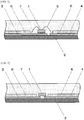
- FIG. 1 illustrates a cross sectional view of an optical semiconductor apparatus of a chip on board (COB) type, which is one example of an optical semiconductor apparatus of the present invention.
- COB chip on board
- FIG. 1 illustrates a cross sectional view of an optical semiconductor apparatus of a chip on board (COB) type, which is one example of an optical semiconductor apparatus of the present invention.
- optical semiconductor element 1 is mounted on substrate 2 for COB via a die bond, so as to electrically connect this optical semiconductor element 1 with circuits 3, 4 via bonding wire 5.
- light reflecting material 6 is formed around the periphery of optical semiconductor element 1 on substrate 2, so as to efficiently well reflect light emitted from optical semiconductor element 1.
- FIG. 2 illustrates a cross sectional view of another optical semiconductor apparatus of a chip on board (COB) type, which is one example of an optical semiconductor apparatus of the present invention.
- COB chip on board
- optical semiconductor element 1 is electrically connected with circuits 3, 4 on substrate 2 for COB via a bonding pad.
- light reflecting material 6 is formed around the periphery of optical semiconductor element 1 on substrate 2, so as to efficiently well reflect light emitted from optical semiconductor element 1.
- substrate 2 may be a metal substrate of aluminum, copper, etc., with circuits 3, 4 formed on the surface of the metal substrate via an insulating layer (not shown).
- the insulating layer need not be formed.
- a nonmetal substrate may include a glass epoxy substrate, a polybutyleneterephthalate (PBT) substrate, a polyimide substrate, a polyester substrate, an aluminum nitride substrate, a boron nitride substrate, a silicon nitride substrate, an alumina ceramics substrate, a glass substrate, and a flexible glass substrate.
- PBT polybutyleneterephthalate
- a hybrid substrate including an aluminum substrate or copper substrate having an insulating resin layer, along with a printed wiring silicon substrate, silicon carbide substrate, or sapphire substrate, can be used.
- an alloy including at least one metal selected from the group consisting of silver, copper, and aluminum having high electric conductivity, or at least one selected from the group consisting of silver, copper, and aluminum is used.
- a primer layer (not shown) formed by the abovementioned primer composition is formed on the surface of circuits 3, 4. Further, in this substrate 2, light reflecting material 6 is formed on circuits 3, 4 via the primer layer so as to expose a portion for mounting optical semiconductor element 1.
- optical semiconductor element 1 and light reflecting material 6 are sealed with sealing material 7
- only optical semiconductor element 1 may be sealed with sealing material 7 in a dome shape.
- FIGS. 1 and 2 while only one optical semiconductor element 1 is illustrated on substrate 2, a plurality of these optical semiconductor elements 1 may be mounted on substrate 2.
- the viscosity is the value at 25°C, with Me, Ph, and Vi representing a methyl group, a phenyl group, and a vinyl group, respectively, in the formulae.
- the softening point of an organosiloxane block copolymer, along with the adhesion performance due to the primer composition was evaluated as follows.
- the organosiloxane block copolymer was molded into a cylindrical tablet shape of ⁇ 14 mm ⁇ 22 mm, this tablet was then placed on a hot plate set to 25°C to 100°C and pressure from above under a load of 100 gram weight was maintained for 10 seconds, after which the load was removed, and subsequently, the deformation amount of the tablet was measured.
- the temperature at which the deformation amount in the height direction reached 1 mm or larger was defined as the softening point.
- a curable silicone composition was applied onto five portions of a glass substrate of 25 mm ⁇ 75 mm using a dispenser in an amount of approximately 100 mg.
- this composition was covered with a 6 mm square aluminum chip having a thickness of 1 mm, pressure-bonded with a plate of 1 kg, heated and cured at 150°C for 2 hours in this state, and subsequently cooled to room temperature to manufacture a die shear test piece.
- the die shear strength of this test piece was measured using a die shear strength measuring apparatus (Bond Tester SS-100KP produced by Seishin Trading Co., Ltd.) to obtain the average value thereof.
- this reaction product is an organosiloxane block copolymer is represented by the average unit formula: (PhMeSiO 2/2 ) 0.55 (PhSiO 3/2 ) 0.45 , in which the phenylsiloxane resin blocks represented by the formula: (PhSiO 3/2 ) are connected with the methylphenylsiloxane blocks represented by the formula: -(PhMeSiO 2/2 ) 140 -, and has 16 mol% of silicon atom-bonded hydroxyl groups and a softening point of 55°C.
- Micron Co. having an average particle diameter of 15 ⁇ m, and 4 parts by mass of dimethylpolysiloxane having a viscosity of 24 mPa ⁇ s, with one terminal of the molecular chain blocked with a dimethylvinylsiloxy group and another terminal of the molecular chain blocked with a trimethoxysiloxy group, and represented by the formula: Me 2 ViSiO(Me 2 SiO) 29 Si(OMe) 3 , were placed in a Ross mixer, mixed at room temperature, and kneaded under reduced pressure while heated to 150°C, to prepare a silicone base.
- the curable silicone composition prepared in Reference Example 3 was applied to a glass plate not subjected to primer treatment, to manufacture a die shear test piece.
- the die shear strength was measured, with the results thereof shown in Table 1.
- the primer composition prepared in Reference Example 2 was uniformly applied onto the glass plate in an application amount of 50 g/m 2 , and dried at 100°C for 30 minutes. The primer layer on the glass plate was uniform.
- the curable silicone composition prepared in Reference Example 3 was applied onto the side of the primer layer of the glass plate to manufacture a die shear test piece. The die shear strength was measured, with the results thereof shown in Table 1. [Table 1] Prac. Example 1 Prac. Example 2 Prac. Example 3 Prac. Example 4 Comp. Example 1 Comp. Example 2 Die shear strength (MPa) 3.4 2.9 1.4 3.1 0.1 0.3
- the primer composition of the present invention improves the adhesion of silicone cured products to base materials of optical semiconductor elements, package materials, substrates, etc., and can suppress peeling or cracking of the silicone cured products caused by heat cycles
- the primer composition is suitable as a primer composition when manufacturing large LED devices having a high calorific value, such as LEDs having high luminance/high output.
Description
- The present invention relates to a primer composition, an adhering method using said composition, and an electric/electronic part using said composition.
- Regarding electric/electronic parts such as optical semiconductor apparatuses (LEDs), an optical semiconductor element is sealed with a silicone cured product in order to improve the reliability thereof. While a curable silicone composition in a hydrosilylation reaction is used in order to form this silicone cured product, the silicone cured product obtained by curing the composition has insufficient adhesion to base materials of optical semiconductor elements, package materials, substrates, etc. In particular, silicone cured products, which have less surface tackiness, less adhesion of dust, etc., and high hardness, have insufficient adhesion to base materials.
- In order to improve the adhesion of silicone cured products to base materials, the base materials are known to be treated with a primer composition in advance. As this primer composition, for example, a primer composition (see Patent Document 1) comprising an acryl-based polymer, a silanol condensation catalyst, and a silane coupling agent; a primer composition (see Patent Document 2) comprising an organosiloxane oligomer having an epoxy group and a silicon atom-binded alkoxy group, and an organic solvent; and a primer composition (see Patent Document 3) comprising a silane coupling agent, an organic aluminum compound of a Lewis acid, and an organic solvent are known.
- Unfortunately, even these primer compositions problematically have insufficient adhesion. Further, due to miniaturization of LEDs, as well as increases in calorific values caused by high luminance of LEDs, in recent years, peeling or cracking problematically tends to occur between the silicone cured product and base materials, under heat cycles.
-
- Patent Document 1: Japanese Unexamined Patent Application Publication No.
2004-339450 - Patent Document 2: Japanese Unexamined Patent Application Publication No.
2006-253398 - Patent Document 3: Japanese Unexamined Patent Application Publication No.
2007-246803 -
WO2013/142240 discloses curable compositions of "resin-linear" organosiloxane block copolymers comprising a metal ligand complex. -
WO2014/152522 discloses curable compositions of resin-linear organosiloxane block copolymers that exhibit stress relaxation behavior are disclosed. -
US2013/245187 relates to organosiloxane block copolymers, curable compositions and solid compositions derived from these block copolymers -
WO2013/090691 discloses curable compositions of "resin-linear" organosiloxane block copolymers comprising a superbase catalyst are disclosed -
WO2014/150841 discloses a solid silicone-containing hot melt composition in powder form. The silicone containing hot melt composition can be a reactive or unreactive silicone-containing hot melt. The composition can be a resin-linear silicone-containing hot melt composition and the composition comprises a phase separated resin-rich phase and a phase separated linear-rich phase. Methods of making optical assemblies and electronic devices comprising such solid silicone-containing hot melt compositions are also disclosed. -
EP0827993 relates to a primer selected from: (i) a mixture of components (A) and (B), (ii) a reaction mixture of components (A) and (B), (iii) component (C), (iv) component (C) and a mixture of components (A) and (B), and (v) component (C) and a reaction mixture of components (A) and (B), where component (A) is silanol-functional organopolysiloxane; component (B) is an epoxy-functional organoalkoxysilane: and component (C) is an organopolysiloxane. - An object of the present invention is to provide a primer composition that improve the adhesion of silicone cured products to base materials of optical semiconductor elements, package materials, substrates, etc., and can suppress peeling or cracking of said silicone cured products caused by heat cycles. Moreover, another object of the present invention is to provide an adhering method that improves the adhesion of silicone cured products to base materials, and can suppress peeling or cracking of said silicone cured products caused by heat cycles. Further, another object of the present invention is to provide an electric/electronic part that improves the adhesion of silicone cured products to base materials, and can suppress peeling or cracking of said silicone cured products caused by heat cycles.
- The present invention is defined by the claims.. The primer composition of the present invention comprises:
- (A) an organosiloxane block copolymer represented by the average unit formula:
(R1 2SiO2/2)a(R2SiO3/2)b
wherein each R1 and R2 is independently an alkyl group having a carbon number of 1 to 12, an aryl group having a carbon number of 6 to 20, or an aralkyl group having a carbon number of 7 to 20, "a" is a number in the range of 0.40 to 0.90, "b" is a number in the range of 0.10 to 0.60, and "a + b" = 1.00,
and having 0.5 to 35.0 mol% of silicon atom-bonded hydroxyl groups or silicon atom-bonded alkoxy groups, in addition to being a solid at 25°C and having a softening point of 200°C or lower,
in which resinous siloxane blocks represented by the formula:
[R2SiO3/2]
wherein R2 is the same as above,
are connected by linear siloxane blocks represented by the formula:
-(R1 2SiO2/2)n-
wherein R1 is the same as above, and "n" is a number in the range of 10 to 400; - (B) a curing catalyst, to promote curing of this composition; and
- (C) an organic solvent.
- The adhering method of the present invention comprises: applying the abovementioned primer composition onto a base material; removing the organic solvent; and subsequently applying a curable silicone composition onto the obtained primer layer for curing.
- The electric/electronic part of the present invention comprises an electric/electronic base material, a primer layer on the base material, and a silicone cured product on the primer layer, wherein the primer layer is formed by the abovementioned primer composition.
- The primer composition of the present invention improves the adhesion of silicone cured products to base materials of optical semiconductor elements, package materials, substrates, etc., and can suppress peeling or cracking of said silicone cured products caused by heat cycles. Moreover, the adhering method of the present invention improves the adhesion of silicone cured products to the base material, and can suppress peeling or cracking of said silicone cured products caused by heat cycles. Further, the electric/electronic part of the present invention improves the adhesion of silicone cured products to the base material, and can suppress peeling or cracking of said silicone cured products caused by heat cycles.
-
-
FIG. 1 is a cross sectional view of an optical semiconductor apparatus of a chip on board (COB) type, which is one example of an electric/electronic part of the present invention. -
FIG. 2 is a cross sectional view of an optical semiconductor apparatus of a chip on board (COB) type, which is one example of another electric/electronic part of the present invention. - An organosiloxane block copolymer for component (A) is represented by the average unit formula:
(R1 2SiO2/2)a(R2SiO3/2)b.
- In the formula, each R1 and R2 is independently an alkyl group having a carbon number of 1 to 12, an aryl group having a carbon number of 6 to 20, or an aralkyl group having a carbon number of 7 to 20. Specific examples thereof may include an alkyl group such as a methyl group, an ethyl group, a propyl group, an isopropyl group, a butyl group, an isobutyl group, a tert-butyl group, a pentyl group, a neopentyl group, a hexyl group, a cyclohexyl group, an octyl group, a nonyl group, and a decyl group; an aryl group such as a phenyl group, a tolyl group, a xylyl group, and a naphthyl group; and an aralkyl group such as a benzyl group, a phenethyl group, and a phenylpropyl group. R1 is preferably an alkyl group and/or an aryl group, particularly preferably a methyl group and/or a phenyl group. R2 is preferably an aryl group, particularly preferably a phenyl group.
- In the formula, "a" is a number in the range of 0.40 to 0.90, preferably a number in the range of 0.50 to 0.90, or a number in the range of 0.60 to 0.90. In the formula, "b" is a number in the range of 0.10 to 0.60, preferably a number in the range of 0.10 to 0.50, or a number in the range of 0.10 to 0.40. Note that in the formula, "a + b + c" = 1.00.
- Further, in component (A), resinous siloxane blocks represented by the formula:
[R2SiO3/2]
are connected with linear siloxane blocks represented by the formula:
-(R1 2SiO2/2)n-.
- In the resinous siloxane blocks represented by the formula:
[R2SiO3/2],
R2 is an alkyl group having a carbon number of 1 to 12, an aryl group having a carbon number of 6 to 20, or an aralkyl group having a carbon number of 7 to 20, exemplified by the same groups as above. Moreover, the weight average molecular weight of this resinous siloxane block is not limited, and preferably at least 500. This means that this resinous siloxane block includes at least three or more trisiloxane units represented by the formula: R2SiO3/2. Note that this weight average molecular weight is derived from a resinous siloxane, which is a raw material, wherein the raw resinous siloxane can be measured via gel permeation chromatography (GPC). - Moreover, in the linear siloxane block represented by the formula:
-(R1 2SiO2/2)n-,
each R1 is independently an alkyl group having a carbon number of 1 to 12, an aryl group having a carbon number of 6 to 20, or an aralkyl group having a carbon number of 7 to 20, exemplified by the same groups as above. - An organosiloxane block copolymer for component (A) comprises a disiloxy [R1 2SiO2/2] unit and a trisiloxy [R2SiO3/2] unit, further comprises 0.5 to 35.0 mol%, preferably 2 to 32 mol% of silicon atom-bonded hydroxyl groups [=SiOH] or silicon atom-bonded alkoxy groups [≡SiOR]. Examples of this alkoxy group may include an alkoxy group having a carbon number of 1 to 4, such as an methoxy group, an ethoxy group, a propoxy group, an isopropoxy group, a butoxy group, an isobutoxy group, or a tert-butoxy group. This silicon atom-bonded hydroxyl group or silicon atom-bonded alkoxy group is present on any siloxy unit in the organosiloxane block copolymer, with this silicon atom-bonded hydroxyl group or silicon atom-bonded alkoxy group capable of being reacted to cure this composition.
- Note that the mol fraction of the disiloxy [R1 2SiO2/2] unit and the trisiloxy [R2SiO3/2] unit in the organosiloxane block copolymer for component (A), as well as the content of the silicon atom-bonded hydroxyl group [≡SiOH] or the silicon atom-bonded alkoxy group [≡SiOR] in the organosiloxane block copolymer, can be measured by 29Si nuclear magnetic resonance spectrum (NMR).
- Component (A) is a solid at 25°C, and has a softening point of 200°C or lower. The preferable upper limit of the softening point is 150°C or lower, or 100°C or lower, while the preferable lower limit thereof is 30°C or higher, or 50°C or higher. Moreover, while the molecular weight of component (A) is not limited, the weight average molecular weight thereof is preferably 20,000 or higher, further preferably 40,000 or higher.
- In the organosiloxane block copolymer for component (A), because the resinous siloxane blocks represented by the formula:
[R2SiO3/2]
are connected with the linear siloxane blocks represented by the formula:
-(R1 2SiO2/2)n-,
and the resinous siloxane blocks are further aggregated to form a "nanodomain" including a "hard" polymer block, this organosiloxane block copolymer is a solid at room temperature. In contrast, a phase separated linear siloxane block forms a "soft" polymer block, and this phase separated "soft" polymer block and a "hard" polymer block includes a "soft" polymer block having a different glass transition temperature (Tg), specifically, a lower Tg such as lower than 25°C, lower than 0°C, or lower than - 20°C, along with a "hard" polymer block having a higher Tg such as higher than 30°C, higher than 40°C, or higher than 50°C. As a result, even when a silicone cured product, which is adhered to base materials of optical semiconductor elements, package materials, substrates, etc. via a primer layer formed by this composition, is subjected to heat cycles, etc., the primer layer can relax stress, and suppress peeling or cracking of the silicone cured product. - The preparation method of such an organosiloxane block copolymer for component (A) is not limited, with it prepared by methods described in, for example, Japanese Translation of
PCT International Application Publication No. 2013-540169 PCT International Application Publication No. 2013-544295 - Component (B) is a curing catalyst to promote curing of this composition, and preferably a condensation reaction catalyst. Examples of such a condensation reaction catalyst may include organic tin compounds such as dibutyltin dilaurate, dibutyltin diacetate, tin octenoate, dibutyltin dioctate, and tin laurate; organic titanium compounds such as tetrabutyl titanate, tetrapropyl titanate, and dibutoxybis(ethylacetoacetate); organic zirconium compounds such as tetrabutyl zirconate, tetrakis(acetylacetonato)zirconium, tetraisobutyl zirconate, butoxytris(acetylacetonato)zirconium, zirconium naphthenate, zirconium octylate, and zirconium 2-ethylhexanoate; organic aluminum compounds such as trimethoxyaluminum, triethoxyaluminum, triisopropoxyaluminum, tri-n-propylaluminum, aluminum naphthenate, aluminum stearate, aluminum octylate, aluminum benzoate, aluminumethylacetoacetatediisopropylate, aluminumethylacetoacetatediisobutyrate, aluminumtris(ethylacetoacetate), aluminumbisethylacetoacetatemonoacetylacetonate, and aluminumtris(acetylacetonate); nitrogen-containing compounds such as 1,8-diazabicyclo[5,4,0]-undeca-7-en (DBU), 1,5,7-triazabicyclo[4.4.0]deca-5-en (TBD), 1,4-diazabicyclo[2.2.0]octane (DABCO), 1,1,3,3-tetramethylguanidine (TMG), 1,5-diazabicyclo[4.3.0]-5-nonene (DBN), and 7-methyl-1,5,7-triazabicyclo[4.4.0]deca-5-en (MTBD); organic phosphorus compounds such as triphenyl phosphine oxide; acidic compounds such as hydrochloric acid, sulfuric acid, and dodecylbenzenesulfonic acid; and alkaline compounds such as ammonia and sodium hydroxide, with organic tin compounds, organic titanium compounds, nitrogen-containing compounds, and alkaline compounds preferable.
- The content of component (B) is an amount to promote curing of this composition, and specifically, with respect to 100 parts by mass of component (A), preferably in the range of 0.005 to 0.5 parts by mass, or in the range of 0.01 to 0.5 parts by mass. This is because when the content of component (B) is the lower limit or more of the abovementioned range, the obtained composition can be sufficiently cured; in contrast, when it is the upper limit or less of the abovementioned range, the mechanical and optical properties of the primer layer obtained by curing the obtained composition are not impaired.
- The organic solvent for component (C) is a component to dissolve component (A) in a solid state at 25°C and improve the coating properties of this composition. Examples of such an organic solvent may include an aliphatic hydrocarbon based solvent such as n-heptane, n-hexane, isooctane, cyclopentane, and cyclohexane; an alcohol-based solvent such as ethanol, propanol, butanol, and cyclohexanol; an ether-based solvent such as diethylether, tetrahydrofuran, and 1,4-dioxane; a ketone-based solvent such as acetone and methylisobutyl ketone; an ester-based solvent such as ethyl acetate and butyl acetate; an aromatic hydrocarbon based solvent such as toluene and xylene; and an aromatic heterocycle-based solvent such as pyridine. Because component (A) can be sufficiently dissolved, component (C) preferably includes an aromatic hydrocarbon based solvent; moreover, because this composition can be uniformly applied to a base material, component (C) is preferably a mixed solvent of an aromatic hydrocarbon based solvent and an aliphatic hydrocarbon based solvent.
- Taking the coating workability and drying workability of this composition into consideration, the content of component (C) is an amount that can be optionally determined, specifically an amount of 70% by mass or higher, preferably in the range of 70 to 99.9% by mass, or in the range of 80 to 99.9% by mass of this overall composition.
- This composition may contain, as other optional components, alkenyl group-containing silane coupling agents such as vinyltrimethoxysilane, vinyltriethoxysilane, allyltrimethoxysilane, and allyltriethoxysilane; epoxy group-containing silane coupling agents such as 3-glycidoxypropyltrimethoxysilane and 2-(3,4-epoxycyclohexyl)ethyltrimethoxysilane; methacryl group- or acryl group-containing silane coupling agents such as 3-methacroxypropyltrimethoxysilane and 3-acryloxypropyltrimethoxysilane; amino group-containing silane coupling agents such as 3-aminopropyltrimethoxysilane, 3-aminopropyltriethoxysilane, and N-(2-ethylamino)-3-aminopropyltrimethoxysilane, etc. The content of the silane coupling agent is not limited, and preferably in the range of 0.05 to 5% by mass, or in the range of 0.1 to 2% by mass of this overall composition.
- Moreover, for the case in which the curable silicone composition to adhere onto the primer layer of the present invention is hydrosilylation reaction curable, it may contain a catalyst for a hydrosilylation reaction in order to improve the curability and adhesion to this primer layer. Examples of a catalyst for such a hydrosilylation reaction may include a platinum-based catalyst, a rhodium-based catalyst, and a palladium-based catalyst, with a platinum-based catalyst preferable because curing of this composition can be significantly promoted. Examples of this platinum-based catalyst may include a platinum fine powder, platinum chloride, an alcohol solution of platinum chloride, a platinum-alkenylsiloxane complex, a platinum-olefin complex, and a platinum-carbonyl complex, with a platinum-alkenylsiloxane complex particularly preferable. Examples of this alkenylsiloxane may include 1,3-divinyl-1,1,3,3-tetramethyldisiloxane, 1,3,5,7-tetramethyl-1,3,5,7-tetravinylcyclotetrasiloxane, alkenylsiloxane obtained by substituting part of a methyl group of these alkenylsiloxanes for an ethyl group, a phenyl group, etc., and alkenylsiloxane obtained by substituting a vinyl group of these alkenylsiloxanes for an allyl group, a hexenyl group, etc. Because the stability of this platinum-alkenylsiloxane complex is particularly favorable, 1,3-divinyl-1,1,3,3-tetramethyldisiloxane is preferable. The content of the catalyst for a hydrosilylation reaction is, with respect to this overall composition, preferably an amount in which metal atoms are in the range of 0.01 to 10,000 ppm in mass units.
- Next, the adhering method of the present invention will be described in detail.
- In the adhering method of the present invention, the abovementioned primer composition is first applied onto the base material.
- The electric/electronic base material is not limited, with examples thereof potentially including an optical semiconductor element, a package material, and a substrate. Moreover, the material of the base material is not limited, with examples thereof potentially including a metal material such as aluminum, copper, nickel, and aluminum nitride; a metal oxide material such as glass and sapphire; an organic material such as an imide resin, a bismaleimide·triazine resin, a glass fiber-containing epoxy resin, a paper phenol resin, bakelite, a polyethyleneterephthalate resin, a polybutyleneterephthalate resin, a polyacrylonitrile resin, a polycarbonate resin, a fluorine resin, a polyimide resin, a polyphenylene sulfide resin, an aramid resin, a polyetherether resin, a polyetherimide resin, a liquid crystal polymer, a polyether sulfone resin, a cycloolefin resin, a silicone rubber, and a silicone resin.
- The application amount of the primer composition is generally 30 to 100 g/m2, preferably 10 to 50 g/m2. This is because, when it is less than the abovementioned lower limit, a primer layer of sufficient thickness cannot be formed, with firm adhesion incapable of being achieved. This is also because, when it is more than the abovementioned upper limit, the primer layer becomes too thick, making it difficult to control the thickness of the curable silicone composition to be adhered.
- As a method for applying the primer composition, conventionally known methods such as spraying, brush coating, and immersion are applicable. While the method for removing the organic solvent is not limited, well-known methods such as a method for drying by being left to stand at room temperature, a method for drying by blowing air, a method for forcibly evaporating the organic solvent by heating, and a method for drying by infrared-ray irradiation can be used. Note that the primer layer may be cured in the process of removing the organic solvent, or may be cured simultaneously upon subsequent curing of the curable silicone composition.
- Next, a curable silicone composition is applied onto the primer layer of the base material for curing. This curable silicone composition is not limited, and is preferably a hydrosilylation reaction curable silicone composition. This hydrosilylation reaction curable silicone composition comprises, for example:
- (I) organopolysiloxane having at least two alkenyl groups in a molecule;
- (II) organopolysiloxane having at least two silicon atom-bonded hydrogen atoms in a molecule; and
- (III) a catalyst for a hydrosilylation reaction.
- Examples of alkenyl groups in component (I) may include a vinyl group, an allyl group, a butenyl group, a pentenyl group, and a hexenyl group. Moreover, examples of groups bonding to silicon atoms other than the alkenyl group in component (I) may include alkyl groups such as a methyl group, an ethyl group, a propyl group, a butyl group, a pentyl group, a hexyl group, and a heptyl group; cycloalkyl groups such as a cyclopentyl group and a cyclohexyl group; aryl groups such as a phenyl group, a tolyl group, a xylyl group, and a naphthyl group; aralkyl groups such as a benzyl group, a phenethyl group, and a 3-phenylpropyl group; and halogenated alkyl groups such as a chloromethyl group, a 3-chloropropyl group, a 3,3,3-trifluoropropyl group, and a nonafluorobutylethyl group.
- The molecular structure of component (I) is not limited, with examples thereof potentially including a linear structure, a cyclic structure, a partially branched linear structure, and a branched structure. Moreover, the viscosity of component (I) is not limited, and preferably in the range of 20 to 100,000 mPa·s, or in the range of 100 to 10,000 mPa·s, at 25°C.
- Examples of groups bonding to silicon atoms other than hydrogen atoms in component (II) may include alkyl groups such as a methyl group, an ethyl group, a propyl group, a butyl group, a pentyl group, a hexyl group, and a heptyl group; cycloalkyl groups such as a cyclopentyl group and a cyclohexyl group; aryl groups such as a phenyl group, a tolyl group, a xylyl group, and a naphthyl group; aralkyl groups such as a benzyl group, a phenethyl group, and a 3-phenylpropyl group; and halogenated alkyl groups such as a chloromethyl group, a 3-chloropropyl group, a 3,3,3-trifluoropropyl group, and a nonafluorobutylethyl group.
- The molecular structure of component (II) is not limited, with examples thereof potentially including a linear structure, a cyclic structure, a partially branched linear structure, and a branched structure. Moreover, the viscosity of component (II) is not limited, and preferably in the range of 1 to 10,000 mPa·s at 25°C.
- The content of component (II) may be a sufficient amount to cure the abovementioned curable silicone composition, and is, with respect to one mol of alkenyl groups in component (I), preferably an amount in which the silicon atom-bonded hydrogen atoms in component (II) are in the range of 0.3 to 10 mols.
- Component (III) is a catalyst for a hydrosilylation reaction to promote curing of the abovementioned curable silicone composition, with the catalyst described above capable of being used.
- The content of component (III) is not limited, and is an amount to promote curing of the abovementioned curable silicone composition, and is, with respect to the abovementioned curable silicone composition, preferably an amount in which the platinum metal is in the range of 1 to 1000 ppm, or an amount in the range of 5 to 100 ppm, in mass units.
- Next, the curable silicone composition is cured on the primer layer. The conditions of curing the curable silicone composition are not limited, with the composition capable of being heated as required.
- Next, the electric/electronic part of the present invention will be described in detail.
- The electric/electronic part of the present invention comprises an electric/electronic base material, a primer layer on the base material, and a silicone cured product on the primer layer, wherein the primer layer is formed by the abovementioned primer composition. Examples of this electric/electronic part may include an optical semiconductor apparatus (LED).
- A cross sectional view of an optical semiconductor apparatus (LED), which is one example of the electric/electronic part of the present invention, is illustrated in
FIGS. 1 and 2. FIG. 1 illustrates a cross sectional view of an optical semiconductor apparatus of a chip on board (COB) type, which is one example of an optical semiconductor apparatus of the present invention. In the optical semiconductor apparatus of a COB type ofFIG. 1 ,optical semiconductor element 1 is mounted onsubstrate 2 for COB via a die bond, so as to electrically connect thisoptical semiconductor element 1 withcircuits bonding wire 5. Moreover,light reflecting material 6 is formed around the periphery ofoptical semiconductor element 1 onsubstrate 2, so as to efficiently well reflect light emitted fromoptical semiconductor element 1. -
FIG. 2 illustrates a cross sectional view of another optical semiconductor apparatus of a chip on board (COB) type, which is one example of an optical semiconductor apparatus of the present invention. In the optical semiconductor apparatus of a COB type ofFIG. 2 ,optical semiconductor element 1 is electrically connected withcircuits substrate 2 for COB via a bonding pad. Moreover,light reflecting material 6 is formed around the periphery ofoptical semiconductor element 1 onsubstrate 2, so as to efficiently well reflect light emitted fromoptical semiconductor element 1. - In the optical semiconductor apparatuses of
FIGS. 1 and 2 ,substrate 2 may be a metal substrate of aluminum, copper, etc., withcircuits substrate 2, the insulating layer need not be formed. Examples of such a nonmetal substrate may include a glass epoxy substrate, a polybutyleneterephthalate (PBT) substrate, a polyimide substrate, a polyester substrate, an aluminum nitride substrate, a boron nitride substrate, a silicon nitride substrate, an alumina ceramics substrate, a glass substrate, and a flexible glass substrate. Further, as thissubstrate 2, a hybrid substrate including an aluminum substrate or copper substrate having an insulating resin layer, along with a printed wiring silicon substrate, silicon carbide substrate, or sapphire substrate, can be used. - As these
circuits circuits substrate 2,light reflecting material 6 is formed oncircuits optical semiconductor element 1. - In
FIGS. 1 and 2 , whileoptical semiconductor element 1 andlight reflecting material 6 are sealed with sealingmaterial 7, onlyoptical semiconductor element 1 may be sealed with sealingmaterial 7 in a dome shape. Note that inFIGS. 1 and 2 , while only oneoptical semiconductor element 1 is illustrated onsubstrate 2, a plurality of theseoptical semiconductor elements 1 may be mounted onsubstrate 2. - The primer composition, the adhering method, and the electric/electronic part of the present invention will be described in detail with reference to examples. In the examples, the viscosity is the value at 25°C, with Me, Ph, and Vi representing a methyl group, a phenyl group, and a vinyl group, respectively, in the formulae. Moreover, the softening point of an organosiloxane block copolymer, along with the adhesion performance due to the primer composition, was evaluated as follows.
- The organosiloxane block copolymer was molded into a cylindrical tablet shape of ϕ14 mm × 22 mm, this tablet was then placed on a hot plate set to 25°C to 100°C and pressure from above under a load of 100 gram weight was maintained for 10 seconds, after which the load was removed, and subsequently, the deformation amount of the tablet was measured. The temperature at which the deformation amount in the height direction reached 1 mm or larger was defined as the softening point.
- A curable silicone composition was applied onto five portions of a glass substrate of 25 mm × 75 mm using a dispenser in an amount of approximately 100 mg. Next, this composition was covered with a 6 mm square aluminum chip having a thickness of 1 mm, pressure-bonded with a plate of 1 kg, heated and cured at 150°C for 2 hours in this state, and subsequently cooled to room temperature to manufacture a die shear test piece. The die shear strength of this test piece was measured using a die shear strength measuring apparatus (Bond Tester SS-100KP produced by Seishin Trading Co., Ltd.) to obtain the average value thereof.
- 45.0 g of an organopolysiloxane resin represented by the average unit formula: PhSiO3/2 and having a weight average molecular weight of 1,300, along with 70.38 g of toluene, was placed in a 500 mL four-neck round-bottom flask equipped with a Dean Stark apparatus with a thermometer, a stirring paddle made of Teflon (registered trademark), and a water cooled condenser installed therein, and heated while stirring under a nitrogen atmosphere. The reaction mixture was heated for 30 minutes while being toluene refluxed, and subsequently cooled to 108°C.
- Moreover, 1.21 g of a mixture having a mass ratio of 1:1 of methyltriacetoxysilane to ethyltriacetoxysilane was added to a solution including 55.0 g of methylphenylpolysiloxane (polymerization degree: 140) having both terminals of the molecular chain blocked with silanol groups and 29.62 g of toluene, to prepare a toluene solution of methylphenylpolysiloxane (polymerization degree: 140) having both terminals of the molecular chain blocked with diacetoxy groups.
- The abovementioned toluene solution of the methylphenylpolysiloxane having both terminals of the molecular chain blocked with diacetoxy groups was rapidly added to the abovementioned reaction mixture under a nitrogen atmosphere, and reacted at room temperature for two hours. Subsequently, the reaction mixture was heated for two hours while being toluene refluxed. Next, this was cooled to 108°C, and 7.99 g of the mixture having a mass ratio of 1:1 of methyltriacetoxysilane to ethyltriacetoxysilane was added. The reaction mixture was further heated for one hour while being toluene refluxed. Next, this was cooled to 90°C, after which 12 mL of ion exchange water was added. The temperature was increased and refluxed, and water was removed via azeotropic distillation. The reaction mixture was again cooled to 90°C, and a further 12 mL of ion exchange water was added. This was heated and refluxed to remove water again. Subsequently, 56.9 g of toluene was removed via distillation to increase the solid content. The obtained reaction product was cooled to room temperature, subsequently pressurized and filtered with a 5.0 µm filter, and toluene used to obtain a toluene solution of a reaction product having a solid concentration of 10% by mass. It was found by 29Si nuclear magnetic resonance spectrum analysis that this reaction product is an organosiloxane block copolymer is represented by the average unit formula:
(PhMeSiO2/2)0.55(PhSiO3/2)0.45,
in which the phenylsiloxane resin blocks represented by the formula:
(PhSiO3/2)
are connected with the methylphenylsiloxane blocks represented by the formula:
-(PhMeSiO2/2)140-,
and has 16 mol% of silicon atom-bonded hydroxyl groups and a softening point of 55°C. - 10 parts by mass of allyltrimethoxysilane was added to 100 parts by mass of n-heptane and mixed, subsequently 2 parts by mass of tetra(n-butyl)titanate was added and uniformly mixed, then 0.1 parts by mass of a complex of platinum chloride and 1,3-divinyltetramethyldisiloxane was added and uniformly mixed to prepare a primer composition.
- 4.4 parts by mass of methylvinylpolysiloxane having a linear methylvinylsiloxane block represented by the formula:
-(MeViSiO)20-
with both terminals of the molecular chain blocked with hydroxyl groups, 4.1 parts by mass of dimethylpolysiloxane having both terminals of the molecular chain blocked with dimethylvinylsiloxy groups and represented by the formula:
Me2ViSiO(Me2SiO)160SiMe2Vi,
51.8 parts by mass of titanium oxide (SX-3103 produced by Sakai Chemical Industry Co., Ltd.) having an average primary particle diameter of 0.2 µm, 30 parts by mass of spherical silica (HS-202 produced by Nippon Steel Materials Co., Ltd. Micron Co.) having an average particle diameter of 15 µm, and 4 parts by mass of dimethylpolysiloxane having a viscosity of 24 mPa·s, with one terminal of the molecular chain blocked with a dimethylvinylsiloxy group and another terminal of the molecular chain blocked with a trimethoxysiloxy group, and represented by the formula:
Me2ViSiO(Me2SiO)29Si(OMe)3,
were placed in a Ross mixer, mixed at room temperature, and kneaded under reduced pressure while heated to 150°C, to prepare a silicone base. - Next, 4.7 parts by mass (an amount of 1.5 mols of silicon atom-bonded hydrogen atoms in this component, with respect to the total of one mol of vinyl groups in methylvinylpolysiloxane and in dimethylpolysiloxane having both terminals of the molecular chain blocked with dimethylvinylsiloxy groups in the silicone base) of methylhydrogenpolysiloxane having a linear methylhydrogensiloxane block represented by the formula:
-(MeHSiO)50-
and having both terminals of the molecular chain blocked with trimethylsiloxy groups, 1 parts by mass of a condensation reaction product having a mass ratio of 1:2 of dimethylsiloxane·methylvinylsiloxane copolymerized oligomer having both terminals of the molecular chain blocked with hydroxyl groups and having a viscosity of 20 mPa·s to 3-glycidoxypropyltrimethoxysilane, and 1-ethinyl-1-cyclohexanol (an amount of 200 ppm in mass units with respect to this composition) were mixed into this silicone base at room temperature, after which a 1,3-divinyl-1,1,3,3-tetramethyldisiloxane solution of 1,3-divinyl-1,1,3,3-tetramethyldisiloxane of platinum (an amount of 3.5 ppm of platinum atoms in mass units with respect to this composition) was mixed to prepare a curable silicone composition. - 5 g of a toluene solution (solid concentration: 10% by mass) of the organosiloxane block copolymer prepared in Reference Example 1, 0.0005 g of 1,8-diazabicyclo[5,4,0]-undeca-7-en (DBU), and 5 g of toluene were uniformly mixed to prepare a primer composition. Next, this primer composition was uniformly applied onto a glass plate in an application amount of 50 g/m2, and dried at 100°C for 30 minutes. The primer layer on the glass plate was slightly spotted and not uniform, but had no surface tackiness. Next, the curable silicone composition prepared in Reference Example 3 was applied on the side of the primer layer of the glass plate to manufacture a die shear test piece. The die shear strength was measured, with the results thereof shown in Table 1.
- 2.5 g of a toluene solution (solid concentration: 10% by mass) of the organosiloxane block copolymer prepared in Reference Example 1, 0.00025 g of 1,8-diazabicyclo[5,4,0]-undeca-7-en (DBU), and 7.5 g of toluene were uniformly mixed to prepare a primer composition. Next, this primer composition was uniformly applied onto a glass plate in an application amount of 50 g/m2, and dried at 100°C for 30 minutes. The primer layer on the glass plate was slightly spotted and not uniform, but had no surface tackiness. Next, the curable silicone composition prepared in Reference Example 3 was applied on the side of the primer layer of the glass plate to manufacture a die shear test piece. The die shear strength was measured, with the results thereof shown in Table 1.
- 1.0 g of a toluene solution (solid concentration: 10% by mass) of the organosiloxane block copolymer prepared in Reference Example 1, 0.0001 g of 1,8-diazabicyclo[5,4,0]-undeca-7-en (DBU), and 9 g of toluene were uniformly mixed to prepare a primer composition. Next, this primer composition was uniformly applied onto a glass plate in an application amount of 50 g/m2, and dried at 100°C for 30 minutes. The primer layer on the glass plate was uniform, and had no surface tackiness. Next, the curable silicone composition prepared in Reference Example 3 was applied onto the side of the primer layer of the glass plate to manufacture a die shear test piece. The die shear strength was measured, with the results thereof shown in Table 1.
- 2.5 g of a toluene solution (solid concentration: 10% by mass) of the organosiloxane block copolymer prepared in Reference Example 1, 0.00025 g of 1,8-diazabicyclo[5,4,0]-undeca-7-en (DBU), 2.5 g of toluene, and 5.0 g of n-heptane were uniformly mixed to prepare a primer composition. Next, this primer composition was uniformly applied onto a glass plate in an application amount of 50 g/m2, and dried at 100°C for 30 minutes. The primer layer on the glass plate was uniform, and had no surface tackiness. Next, the curable silicone composition prepared in Reference Example 3 was applied onto the side of the primer layer of the glass plate to manufacture a die shear test piece. The die shear strength was measured, with the results thereof shown in Table 1.
- The curable silicone composition prepared in Reference Example 3 was applied to a glass plate not subjected to primer treatment, to manufacture a die shear test piece. The die shear strength was measured, with the results thereof shown in Table 1.
- The primer composition prepared in Reference Example 2 was uniformly applied onto the glass plate in an application amount of 50 g/m2, and dried at 100°C for 30 minutes. The primer layer on the glass plate was uniform. Next, the curable silicone composition prepared in Reference Example 3 was applied onto the side of the primer layer of the glass plate to manufacture a die shear test piece. The die shear strength was measured, with the results thereof shown in Table 1.
[Table 1] Prac. Example 1 Prac. Example 2 Prac. Example 3 Prac. Example 4 Comp. Example 1 Comp. Example 2 Die shear strength (MPa) 3.4 2.9 1.4 3.1 0.1 0.3 - Because the primer composition of the present invention improves the adhesion of silicone cured products to base materials of optical semiconductor elements, package materials, substrates, etc., and can suppress peeling or cracking of the silicone cured products caused by heat cycles, the primer composition is suitable as a primer composition when manufacturing large LED devices having a high calorific value, such as LEDs having high luminance/high output.
-
- 1
- optical semiconductor element
- 2
- substrate
- 3
- circuit
- 4
- circuit
- 5
- bonding wire
- 6
- light reflecting material
- 7
- cured product of a curable silicone composition
Claims (8)
- An electric/electronic part comprising an electric/electronic base material, a silicone cured product, and a primer layer adhering the silicone cured product to the base material,
wherein the primer layer comprises the reaction product of a primer composition comprising:(A) an organosiloxane block copolymer represented by the average unit formula:
(R1 2SiO2/2)a(R2SiO3/2)b
wherein each R1 and R2 is independently an alkyl group having a carbon number of 1 to 12, an aryl group having a carbon number of 6 to 20, or an aralkyl group having a carbon number of 7 to 20, "a" is a number in the range of 0.40 to 0.90, "b" is a number in the range of 0.10 to 0.60, and "a + b" = 1.00,
having 0.5 to 35.0 mol% of silicon atom-bonded hydroxyl groups or silicon atom-bonded alkoxy groups, in addition to being a solid at 25°C and having a softening point of 200°C or lower,
in which resinous siloxane blocks represented by the formula:
[R2SiO3/2]
wherein R2 is the same as above,
are connected by linear siloxane blocks represented by the formula:
-(R1 2SiO2/2)n-
wherein R1 is the same as above, and "n" is a number in the range of 10 to 400;(B) a curing catalyst to promote curing of this composition; and(C) an organic solvent; andwherein the silicone cured product is a cured product of a hydrosilylation reaction curable silicone composition. - The electric/electronic part according to Claim 1, wherein R1 in component (A) is an alkyl group or an aryl group.
- The electric/electronic part according to Claim 1 or 2, wherein R2 in component (A) is an aryl group.
- The electric/electronic part according to Claim 1, wherein component (B) is a condensation reaction catalyst.
- The electric/electronic part according to Claim 1, wherein component (C) is an aromatic hydrocarbon based solvent, or a mixed solvent of the aromatic hydrocarbon based solvent and an aliphatic hydrocarbon based solvent.
- A method of forming an electric/electronic part comprising: applying a primer composition onto an electric/electronic base material;
removing an organic solvent to obtain a primer layer; and
subsequently applying a hydrosilylation curable silicone composition onto the obtained primer layer for curing to form a silicone cured product,
wherein the primer composition comprises:(A) an organosiloxane block copolymer represented by the average unit formula:
(R1 2SiO2/2)a(R2SiO3/2)b
wherein each R1 and R2 is independently an alkyl group having a carbon number of 1 to 12, an aryl group having a carbon number of 6 to 20, or an aralkyl group having a carbon number of 7 to 20, "a" is a number in the range of 0.40 to 0.90, "b" is a number in the range of 0.10 to 0.60, and "a + b" = 1.00,
having 0.5 to 35.0 mol% of silicon atom-bonded hydroxyl groups or silicon atom-bonded alkoxy groups, in addition to being a solid at 25°C and having a softening point of 200°C or lower,
in which resinous siloxane blocks represented by the formula:
[R2SiO3/2]
wherein R2 is the same as above,
are connected by linear siloxane blocks represented by the formula:
-(R1 2SiO2/2)n-
wherein R1 is the same as above, and "n" is a number in the range of 10 to 400;(B) a curing catalyst to promote curing of this composition; and(C) an organic solvent. - The method according to Claim 6, wherein the hydrosilylation curable silicone composition and the primer layer are simultaneously cured.
- The electric/electronic part according to Claim 1, wherein the electric/electronic part is an optical semiconductor apparatus.
Applications Claiming Priority (2)
| Application Number | Priority Date | Filing Date | Title |
|---|---|---|---|
| JP2015037452 | 2015-02-26 | ||
| PCT/JP2016/000960 WO2016136244A1 (en) | 2015-02-26 | 2016-02-23 | Primer composition, bonding method, and electric/electronic component |
Publications (3)
| Publication Number | Publication Date |
|---|---|
| EP3275955A1 EP3275955A1 (en) | 2018-01-31 |
| EP3275955A4 EP3275955A4 (en) | 2018-08-01 |
| EP3275955B1 true EP3275955B1 (en) | 2020-05-27 |
Family
ID=56788337
Family Applications (1)
| Application Number | Title | Priority Date | Filing Date |
|---|---|---|---|
| EP16754994.8A Active EP3275955B1 (en) | 2015-02-26 | 2016-02-23 | Electric/electronic part and bonding method |
Country Status (7)
| Country | Link |
|---|---|
| US (1) | US10479910B2 (en) |
| EP (1) | EP3275955B1 (en) |
| JP (1) | JP6666896B2 (en) |
| KR (1) | KR20170124558A (en) |
| CN (1) | CN107429115A (en) |
| TW (1) | TWI682009B (en) |
| WO (1) | WO2016136244A1 (en) |
Families Citing this family (5)
| Publication number | Priority date | Publication date | Assignee | Title |
|---|---|---|---|---|
| HUE045274T2 (en) | 2013-01-09 | 2019-12-30 | Basf Agro Bv | Process for the preparation of substituted oxiranes and triazoles |
| JP6447557B2 (en) * | 2016-03-24 | 2019-01-09 | 日亜化学工業株式会社 | Method for manufacturing light emitting device |
| US11072593B2 (en) | 2016-06-15 | 2021-07-27 | BASF Agro B.V. | Process for the epoxidation of a tetrasubstituted alkene |
| CN113677769B (en) * | 2019-04-29 | 2023-06-06 | 美国陶氏有机硅公司 | Primer for silicone rubber compositions and elastomeric materials |
| CN113717637B (en) * | 2021-09-07 | 2022-08-02 | 河南三棵树新材料科技有限公司 | High-temperature-resistant anticorrosive paint and preparation method thereof |
Family Cites Families (14)
| Publication number | Priority date | Publication date | Assignee | Title |
|---|---|---|---|---|
| BE759621A (en) * | 1969-12-01 | 1971-06-01 | Dow Corning | COPOLYMER SEQUENCES OF NON-CORROSIVE ORGANOSILOXANES, VULCANIZABLE AT ROOM TEMPERATURE |
| JP3527369B2 (en) | 1996-09-04 | 2004-05-17 | 東レ・ダウコーニング・シリコーン株式会社 | Electric component and method of manufacturing the same |
| JP4041966B2 (en) | 2002-06-18 | 2008-02-06 | 信越化学工業株式会社 | Article with hard coat agent and hard coat film formed |
| JP2004339450A (en) | 2003-05-19 | 2004-12-02 | Kanegafuchi Chem Ind Co Ltd | Primer composition and light emitting diode using the primer composition |
| JP4623282B2 (en) | 2005-03-10 | 2011-02-02 | 信越化学工業株式会社 | Manufacturing method of semiconductor device |
| JP4777802B2 (en) | 2006-03-17 | 2011-09-21 | 信越化学工業株式会社 | Light-resistant primer composition, method for producing light-emitting semiconductor device using the primer composition, and light-emitting semiconductor device obtained by the method |
| CN103189421B (en) * | 2010-09-22 | 2015-03-25 | 道康宁公司 | Organosiloxane block copolymer |
| KR101807190B1 (en) * | 2010-09-22 | 2017-12-08 | 다우 코닝 코포레이션 | Process for preparing resin-linear organosiloxane block copolymers |
| EP2670789A1 (en) * | 2011-02-04 | 2013-12-11 | Dow Corning Corporation | Curable organosiloxane block copolymer emulsions |
| US9650472B2 (en) * | 2011-12-14 | 2017-05-16 | Dow Corning Corporation | Curable compositions of resin-linear organosiloxane block copolymers |
| WO2013142240A1 (en) * | 2012-03-21 | 2013-09-26 | Dow Corning Corporation | Compositions of resin-linear organosiloxane block copolymers |
| WO2014129347A1 (en) * | 2013-02-20 | 2014-08-28 | 横浜ゴム株式会社 | Curable resin composition |
| KR20150133779A (en) * | 2013-03-15 | 2015-11-30 | 다우 코닝 코포레이션 | A method for making an optical assembly comprising depositing a solid silicone-containing hot melt composition in powder form and forming an encapsulant thereof |
| JP2016517463A (en) | 2013-03-15 | 2016-06-16 | ダウ コーニング コーポレーションDow Corning Corporation | Resin-linear organosiloxane block copolymer composition |
-
2016
- 2016-02-23 WO PCT/JP2016/000960 patent/WO2016136244A1/en active Application Filing
- 2016-02-23 JP JP2017501937A patent/JP6666896B2/en active Active
- 2016-02-23 KR KR1020177025928A patent/KR20170124558A/en active IP Right Grant
- 2016-02-23 US US15/553,407 patent/US10479910B2/en not_active Expired - Fee Related
- 2016-02-23 EP EP16754994.8A patent/EP3275955B1/en active Active
- 2016-02-23 CN CN201680015993.7A patent/CN107429115A/en active Pending
- 2016-02-24 TW TW105105532A patent/TWI682009B/en active
Non-Patent Citations (1)
| Title |
|---|
| None * |
Also Published As
| Publication number | Publication date |
|---|---|
| TWI682009B (en) | 2020-01-11 |
| EP3275955A1 (en) | 2018-01-31 |
| WO2016136244A1 (en) | 2016-09-01 |
| TW201638256A (en) | 2016-11-01 |
| EP3275955A4 (en) | 2018-08-01 |
| CN107429115A (en) | 2017-12-01 |
| KR20170124558A (en) | 2017-11-10 |
| JPWO2016136244A1 (en) | 2017-12-07 |
| US10479910B2 (en) | 2019-11-19 |
| JP6666896B2 (en) | 2020-03-18 |
| US20180105720A1 (en) | 2018-04-19 |
Similar Documents
| Publication | Publication Date | Title |
|---|---|---|
| EP3275955B1 (en) | Electric/electronic part and bonding method | |
| TWI756250B (en) | Curable granulated silicone composition, semiconductor article thereof, and manufacturing process thereof | |
| EP3498780B1 (en) | Curable particulate silicone composition, semiconductor member comprising curable particulate silicone composition, and molding method for semiconductor member comprising curable particulate silicone composition | |
| KR101836962B1 (en) | New organosilicon compound, thermosetting resin composition containing the organosilicon compound, hardening resin and encapsulation material for optical semiconductor | |
| EP2721108B1 (en) | Cross-linkable silicone composition and cross-linked product thereof | |
| EP3020750A1 (en) | Adhesiveness-imparting agent, adhesive polyorganosiloxane composition, and optical semiconductor device | |
| KR20110053470A (en) | Curable organopolysiloxane composition, optical semiconductor element sealant, and optical semiconductor device | |
| CN113330071B (en) | Curable silicone composition, cured product thereof, and method for producing same | |
| KR101560038B1 (en) | Curable composition | |
| KR20170052649A (en) | Curable silicone composition, cured object obtained therefrom, and optical semiconductor device | |
| KR101560042B1 (en) | Curable composition | |
| EP2599836B1 (en) | Curable composition for semiconductor encapsulation | |
| EP2733160A1 (en) | Organo polysiloxane, and method for producing same | |
| EP3954739A1 (en) | Curable silicone composition, cured product of same, and method for manufacturing same | |
| CN114945634A (en) | Curable polyorganosiloxane composition, cured product thereof, protective agent or adhesive, and electrical/electronic device | |
| KR20190050999A (en) | Curable resin composition, cured product thereof, and semiconductor device | |
| JPH11243100A (en) | Manufacture of semiconductor-element package and organopolysiloxane composition using the same | |
| CN115003760A (en) | Curable polyorganosiloxane composition, cured product thereof, protective agent or adhesive, and electric/electronic device | |
| EP2878638B1 (en) | Hardening composition | |
| EP2878634A1 (en) | Curable composition | |
| EP2960295B1 (en) | Curable composition | |
| EP2878637B1 (en) | Hardening composition | |
| KR101591185B1 (en) | Curable composition | |
| EP2878635B1 (en) | Hardening composition | |
| TWI831733B (en) | Curable granulated silicone composition, semiconductor article thereof, and molding process thereof |
Legal Events
| Date | Code | Title | Description |
|---|---|---|---|
| STAA | Information on the status of an ep patent application or granted ep patent |
Free format text: STATUS: THE INTERNATIONAL PUBLICATION HAS BEEN MADE |
|
| PUAI | Public reference made under article 153(3) epc to a published international application that has entered the european phase |
Free format text: ORIGINAL CODE: 0009012 |
|
| STAA | Information on the status of an ep patent application or granted ep patent |
Free format text: STATUS: REQUEST FOR EXAMINATION WAS MADE |
|
| 17P | Request for examination filed |
Effective date: 20170823 |
|
| AK | Designated contracting states |
Kind code of ref document: A1 Designated state(s): AL AT BE BG CH CY CZ DE DK EE ES FI FR GB GR HR HU IE IS IT LI LT LU LV MC MK MT NL NO PL PT RO RS SE SI SK SM TR |
|
| AX | Request for extension of the european patent |
Extension state: BA ME |
|
| DAV | Request for validation of the european patent (deleted) | ||
| DAX | Request for extension of the european patent (deleted) | ||
| A4 | Supplementary search report drawn up and despatched |
Effective date: 20180703 |
|
| RIC1 | Information provided on ipc code assigned before grant |
Ipc: C09D 183/10 20060101AFI20180627BHEP Ipc: C09D 7/40 20180101ALI20180627BHEP Ipc: C09D 5/00 20060101ALI20180627BHEP |
|
| RIC1 | Information provided on ipc code assigned before grant |
Ipc: C09D 7/40 20180101ALI20180627BHEP Ipc: C09D 183/10 20060101AFI20180627BHEP Ipc: C09D 5/00 20060101ALI20180627BHEP |
|
| STAA | Information on the status of an ep patent application or granted ep patent |
Free format text: STATUS: EXAMINATION IS IN PROGRESS |
|
| 17Q | First examination report despatched |
Effective date: 20190705 |
|
| RAP1 | Party data changed (applicant data changed or rights of an application transferred) |
Owner name: DOW TORAY CO., LTD. |
|
| GRAP | Despatch of communication of intention to grant a patent |
Free format text: ORIGINAL CODE: EPIDOSNIGR1 |
|
| STAA | Information on the status of an ep patent application or granted ep patent |
Free format text: STATUS: GRANT OF PATENT IS INTENDED |
|
| INTG | Intention to grant announced |
Effective date: 20200120 |
|
| RIN1 | Information on inventor provided before grant (corrected) |
Inventor name: YOSHIDA, SHIN Inventor name: YAMAZAKI, RYOSUKE Inventor name: YOSHIDA, HIROAKI |
|
| GRAS | Grant fee paid |
Free format text: ORIGINAL CODE: EPIDOSNIGR3 |
|
| GRAA | (expected) grant |
Free format text: ORIGINAL CODE: 0009210 |
|
| STAA | Information on the status of an ep patent application or granted ep patent |
Free format text: STATUS: THE PATENT HAS BEEN GRANTED |
|
| AK | Designated contracting states |
Kind code of ref document: B1 Designated state(s): AL AT BE BG CH CY CZ DE DK EE ES FI FR GB GR HR HU IE IS IT LI LT LU LV MC MK MT NL NO PL PT RO RS SE SI SK SM TR |
|
| REG | Reference to a national code |
Ref country code: GB Ref legal event code: FG4D |
|
| REG | Reference to a national code |
Ref country code: CH Ref legal event code: EP |
|
| REG | Reference to a national code |
Ref country code: DE Ref legal event code: R096 Ref document number: 602016037083 Country of ref document: DE |
|
| REG | Reference to a national code |
Ref country code: AT Ref legal event code: REF Ref document number: 1274531 Country of ref document: AT Kind code of ref document: T Effective date: 20200615 |
|
| REG | Reference to a national code |
Ref country code: LT Ref legal event code: MG4D |
|
| PG25 | Lapsed in a contracting state [announced via postgrant information from national office to epo] |
Ref country code: GR Free format text: LAPSE BECAUSE OF FAILURE TO SUBMIT A TRANSLATION OF THE DESCRIPTION OR TO PAY THE FEE WITHIN THE PRESCRIBED TIME-LIMIT Effective date: 20200828 Ref country code: LT Free format text: LAPSE BECAUSE OF FAILURE TO SUBMIT A TRANSLATION OF THE DESCRIPTION OR TO PAY THE FEE WITHIN THE PRESCRIBED TIME-LIMIT Effective date: 20200527 Ref country code: SE Free format text: LAPSE BECAUSE OF FAILURE TO SUBMIT A TRANSLATION OF THE DESCRIPTION OR TO PAY THE FEE WITHIN THE PRESCRIBED TIME-LIMIT Effective date: 20200527 Ref country code: NO Free format text: LAPSE BECAUSE OF FAILURE TO SUBMIT A TRANSLATION OF THE DESCRIPTION OR TO PAY THE FEE WITHIN THE PRESCRIBED TIME-LIMIT Effective date: 20200827 Ref country code: FI Free format text: LAPSE BECAUSE OF FAILURE TO SUBMIT A TRANSLATION OF THE DESCRIPTION OR TO PAY THE FEE WITHIN THE PRESCRIBED TIME-LIMIT Effective date: 20200527 Ref country code: IS Free format text: LAPSE BECAUSE OF FAILURE TO SUBMIT A TRANSLATION OF THE DESCRIPTION OR TO PAY THE FEE WITHIN THE PRESCRIBED TIME-LIMIT Effective date: 20200927 Ref country code: PT Free format text: LAPSE BECAUSE OF FAILURE TO SUBMIT A TRANSLATION OF THE DESCRIPTION OR TO PAY THE FEE WITHIN THE PRESCRIBED TIME-LIMIT Effective date: 20200928 |
|
| REG | Reference to a national code |
Ref country code: NL Ref legal event code: MP Effective date: 20200527 |
|
| PG25 | Lapsed in a contracting state [announced via postgrant information from national office to epo] |
Ref country code: HR Free format text: LAPSE BECAUSE OF FAILURE TO SUBMIT A TRANSLATION OF THE DESCRIPTION OR TO PAY THE FEE WITHIN THE PRESCRIBED TIME-LIMIT Effective date: 20200527 Ref country code: LV Free format text: LAPSE BECAUSE OF FAILURE TO SUBMIT A TRANSLATION OF THE DESCRIPTION OR TO PAY THE FEE WITHIN THE PRESCRIBED TIME-LIMIT Effective date: 20200527 Ref country code: RS Free format text: LAPSE BECAUSE OF FAILURE TO SUBMIT A TRANSLATION OF THE DESCRIPTION OR TO PAY THE FEE WITHIN THE PRESCRIBED TIME-LIMIT Effective date: 20200527 Ref country code: BG Free format text: LAPSE BECAUSE OF FAILURE TO SUBMIT A TRANSLATION OF THE DESCRIPTION OR TO PAY THE FEE WITHIN THE PRESCRIBED TIME-LIMIT Effective date: 20200827 |
|
| REG | Reference to a national code |
Ref country code: AT Ref legal event code: MK05 Ref document number: 1274531 Country of ref document: AT Kind code of ref document: T Effective date: 20200527 |
|
| PG25 | Lapsed in a contracting state [announced via postgrant information from national office to epo] |
Ref country code: NL Free format text: LAPSE BECAUSE OF FAILURE TO SUBMIT A TRANSLATION OF THE DESCRIPTION OR TO PAY THE FEE WITHIN THE PRESCRIBED TIME-LIMIT Effective date: 20200527 Ref country code: AL Free format text: LAPSE BECAUSE OF FAILURE TO SUBMIT A TRANSLATION OF THE DESCRIPTION OR TO PAY THE FEE WITHIN THE PRESCRIBED TIME-LIMIT Effective date: 20200527 |
|
| PG25 | Lapsed in a contracting state [announced via postgrant information from national office to epo] |
Ref country code: CZ Free format text: LAPSE BECAUSE OF FAILURE TO SUBMIT A TRANSLATION OF THE DESCRIPTION OR TO PAY THE FEE WITHIN THE PRESCRIBED TIME-LIMIT Effective date: 20200527 Ref country code: IT Free format text: LAPSE BECAUSE OF FAILURE TO SUBMIT A TRANSLATION OF THE DESCRIPTION OR TO PAY THE FEE WITHIN THE PRESCRIBED TIME-LIMIT Effective date: 20200527 Ref country code: RO Free format text: LAPSE BECAUSE OF FAILURE TO SUBMIT A TRANSLATION OF THE DESCRIPTION OR TO PAY THE FEE WITHIN THE PRESCRIBED TIME-LIMIT Effective date: 20200527 Ref country code: AT Free format text: LAPSE BECAUSE OF FAILURE TO SUBMIT A TRANSLATION OF THE DESCRIPTION OR TO PAY THE FEE WITHIN THE PRESCRIBED TIME-LIMIT Effective date: 20200527 Ref country code: EE Free format text: LAPSE BECAUSE OF FAILURE TO SUBMIT A TRANSLATION OF THE DESCRIPTION OR TO PAY THE FEE WITHIN THE PRESCRIBED TIME-LIMIT Effective date: 20200527 Ref country code: SM Free format text: LAPSE BECAUSE OF FAILURE TO SUBMIT A TRANSLATION OF THE DESCRIPTION OR TO PAY THE FEE WITHIN THE PRESCRIBED TIME-LIMIT Effective date: 20200527 Ref country code: ES Free format text: LAPSE BECAUSE OF FAILURE TO SUBMIT A TRANSLATION OF THE DESCRIPTION OR TO PAY THE FEE WITHIN THE PRESCRIBED TIME-LIMIT Effective date: 20200527 Ref country code: DK Free format text: LAPSE BECAUSE OF FAILURE TO SUBMIT A TRANSLATION OF THE DESCRIPTION OR TO PAY THE FEE WITHIN THE PRESCRIBED TIME-LIMIT Effective date: 20200527 |
|
| PG25 | Lapsed in a contracting state [announced via postgrant information from national office to epo] |
Ref country code: SK Free format text: LAPSE BECAUSE OF FAILURE TO SUBMIT A TRANSLATION OF THE DESCRIPTION OR TO PAY THE FEE WITHIN THE PRESCRIBED TIME-LIMIT Effective date: 20200527 Ref country code: PL Free format text: LAPSE BECAUSE OF FAILURE TO SUBMIT A TRANSLATION OF THE DESCRIPTION OR TO PAY THE FEE WITHIN THE PRESCRIBED TIME-LIMIT Effective date: 20200527 |
|
| REG | Reference to a national code |
Ref country code: DE Ref legal event code: R097 Ref document number: 602016037083 Country of ref document: DE |
|
| PLBE | No opposition filed within time limit |
Free format text: ORIGINAL CODE: 0009261 |
|
| STAA | Information on the status of an ep patent application or granted ep patent |
Free format text: STATUS: NO OPPOSITION FILED WITHIN TIME LIMIT |
|
| 26N | No opposition filed |
Effective date: 20210302 |
|
| PG25 | Lapsed in a contracting state [announced via postgrant information from national office to epo] |
Ref country code: SI Free format text: LAPSE BECAUSE OF FAILURE TO SUBMIT A TRANSLATION OF THE DESCRIPTION OR TO PAY THE FEE WITHIN THE PRESCRIBED TIME-LIMIT Effective date: 20200527 |
|
| PG25 | Lapsed in a contracting state [announced via postgrant information from national office to epo] |
Ref country code: MC Free format text: LAPSE BECAUSE OF FAILURE TO SUBMIT A TRANSLATION OF THE DESCRIPTION OR TO PAY THE FEE WITHIN THE PRESCRIBED TIME-LIMIT Effective date: 20200527 |
|
| GBPC | Gb: european patent ceased through non-payment of renewal fee |
Effective date: 20210223 |
|
| REG | Reference to a national code |
Ref country code: BE Ref legal event code: MM Effective date: 20210228 |
|
| PG25 | Lapsed in a contracting state [announced via postgrant information from national office to epo] |
Ref country code: CH Free format text: LAPSE BECAUSE OF NON-PAYMENT OF DUE FEES Effective date: 20210228 Ref country code: LI Free format text: LAPSE BECAUSE OF NON-PAYMENT OF DUE FEES Effective date: 20210228 Ref country code: LU Free format text: LAPSE BECAUSE OF NON-PAYMENT OF DUE FEES Effective date: 20210223 |
|
| PG25 | Lapsed in a contracting state [announced via postgrant information from national office to epo] |
Ref country code: IE Free format text: LAPSE BECAUSE OF NON-PAYMENT OF DUE FEES Effective date: 20210223 Ref country code: FR Free format text: LAPSE BECAUSE OF NON-PAYMENT OF DUE FEES Effective date: 20210228 Ref country code: GB Free format text: LAPSE BECAUSE OF NON-PAYMENT OF DUE FEES Effective date: 20210223 |
|
| PG25 | Lapsed in a contracting state [announced via postgrant information from national office to epo] |
Ref country code: BE Free format text: LAPSE BECAUSE OF NON-PAYMENT OF DUE FEES Effective date: 20210228 |
|
| PGFP | Annual fee paid to national office [announced via postgrant information from national office to epo] |
Ref country code: DE Payment date: 20221229 Year of fee payment: 8 |
|
| PG25 | Lapsed in a contracting state [announced via postgrant information from national office to epo] |
Ref country code: CY Free format text: LAPSE BECAUSE OF FAILURE TO SUBMIT A TRANSLATION OF THE DESCRIPTION OR TO PAY THE FEE WITHIN THE PRESCRIBED TIME-LIMIT Effective date: 20200527 |
|
| PG25 | Lapsed in a contracting state [announced via postgrant information from national office to epo] |
Ref country code: HU Free format text: LAPSE BECAUSE OF FAILURE TO SUBMIT A TRANSLATION OF THE DESCRIPTION OR TO PAY THE FEE WITHIN THE PRESCRIBED TIME-LIMIT; INVALID AB INITIO Effective date: 20160223 |