EP3273493A1 - Method for manufacturing light emitting device - Google Patents
Method for manufacturing light emitting device Download PDFInfo
- Publication number
- EP3273493A1 EP3273493A1 EP16764834.4A EP16764834A EP3273493A1 EP 3273493 A1 EP3273493 A1 EP 3273493A1 EP 16764834 A EP16764834 A EP 16764834A EP 3273493 A1 EP3273493 A1 EP 3273493A1
- Authority
- EP
- European Patent Office
- Prior art keywords
- wiring board
- led element
- temperature
- conductive adhesive
- anisotropic conductive
- Prior art date
- Legal status (The legal status is an assumption and is not a legal conclusion. Google has not performed a legal analysis and makes no representation as to the accuracy of the status listed.)
- Granted
Links
Images

Classifications
-
- C—CHEMISTRY; METALLURGY
- C09—DYES; PAINTS; POLISHES; NATURAL RESINS; ADHESIVES; COMPOSITIONS NOT OTHERWISE PROVIDED FOR; APPLICATIONS OF MATERIALS NOT OTHERWISE PROVIDED FOR
- C09J—ADHESIVES; NON-MECHANICAL ASPECTS OF ADHESIVE PROCESSES IN GENERAL; ADHESIVE PROCESSES NOT PROVIDED FOR ELSEWHERE; USE OF MATERIALS AS ADHESIVES
- C09J5/00—Adhesive processes in general; Adhesive processes not provided for elsewhere, e.g. relating to primers
- C09J5/06—Adhesive processes in general; Adhesive processes not provided for elsewhere, e.g. relating to primers involving heating of the applied adhesive
-
- H—ELECTRICITY
- H10—SEMICONDUCTOR DEVICES; ELECTRIC SOLID-STATE DEVICES NOT OTHERWISE PROVIDED FOR
- H10H—INORGANIC LIGHT-EMITTING SEMICONDUCTOR DEVICES HAVING POTENTIAL BARRIERS
- H10H20/00—Individual inorganic light-emitting semiconductor devices having potential barriers, e.g. light-emitting diodes [LED]
- H10H20/01—Manufacture or treatment
-
- C—CHEMISTRY; METALLURGY
- C08—ORGANIC MACROMOLECULAR COMPOUNDS; THEIR PREPARATION OR CHEMICAL WORKING-UP; COMPOSITIONS BASED THEREON
- C08G—MACROMOLECULAR COMPOUNDS OBTAINED OTHERWISE THAN BY REACTIONS ONLY INVOLVING UNSATURATED CARBON-TO-CARBON BONDS
- C08G59/00—Polycondensates containing more than one epoxy group per molecule; Macromolecules obtained by polymerising compounds containing more than one epoxy group per molecule using curing agents or catalysts which react with the epoxy groups
- C08G59/18—Macromolecules obtained by polymerising compounds containing more than one epoxy group per molecule using curing agents or catalysts which react with the epoxy groups ; e.g. general methods of curing
- C08G59/68—Macromolecules obtained by polymerising compounds containing more than one epoxy group per molecule using curing agents or catalysts which react with the epoxy groups ; e.g. general methods of curing characterised by the catalysts used
- C08G59/70—Chelates
-
- C—CHEMISTRY; METALLURGY
- C09—DYES; PAINTS; POLISHES; NATURAL RESINS; ADHESIVES; COMPOSITIONS NOT OTHERWISE PROVIDED FOR; APPLICATIONS OF MATERIALS NOT OTHERWISE PROVIDED FOR
- C09J—ADHESIVES; NON-MECHANICAL ASPECTS OF ADHESIVE PROCESSES IN GENERAL; ADHESIVE PROCESSES NOT PROVIDED FOR ELSEWHERE; USE OF MATERIALS AS ADHESIVES
- C09J11/00—Features of adhesives not provided for in group C09J9/00, e.g. additives
- C09J11/02—Non-macromolecular additives
- C09J11/06—Non-macromolecular additives organic
-
- C—CHEMISTRY; METALLURGY
- C09—DYES; PAINTS; POLISHES; NATURAL RESINS; ADHESIVES; COMPOSITIONS NOT OTHERWISE PROVIDED FOR; APPLICATIONS OF MATERIALS NOT OTHERWISE PROVIDED FOR
- C09J—ADHESIVES; NON-MECHANICAL ASPECTS OF ADHESIVE PROCESSES IN GENERAL; ADHESIVE PROCESSES NOT PROVIDED FOR ELSEWHERE; USE OF MATERIALS AS ADHESIVES
- C09J183/00—Adhesives based on macromolecular compounds obtained by reactions forming in the main chain of the macromolecule a linkage containing silicon, with or without sulfur, nitrogen, oxygen, or carbon only; Adhesives based on derivatives of such polymers
- C09J183/04—Polysiloxanes
-
- C—CHEMISTRY; METALLURGY
- C09—DYES; PAINTS; POLISHES; NATURAL RESINS; ADHESIVES; COMPOSITIONS NOT OTHERWISE PROVIDED FOR; APPLICATIONS OF MATERIALS NOT OTHERWISE PROVIDED FOR
- C09J—ADHESIVES; NON-MECHANICAL ASPECTS OF ADHESIVE PROCESSES IN GENERAL; ADHESIVE PROCESSES NOT PROVIDED FOR ELSEWHERE; USE OF MATERIALS AS ADHESIVES
- C09J9/00—Adhesives characterised by their physical nature or the effects produced, e.g. glue sticks
- C09J9/02—Electrically-conducting adhesives
-
- C—CHEMISTRY; METALLURGY
- C23—COATING METALLIC MATERIAL; COATING MATERIAL WITH METALLIC MATERIAL; CHEMICAL SURFACE TREATMENT; DIFFUSION TREATMENT OF METALLIC MATERIAL; COATING BY VACUUM EVAPORATION, BY SPUTTERING, BY ION IMPLANTATION OR BY CHEMICAL VAPOUR DEPOSITION, IN GENERAL; INHIBITING CORROSION OF METALLIC MATERIAL OR INCRUSTATION IN GENERAL
- C23C—COATING METALLIC MATERIAL; COATING MATERIAL WITH METALLIC MATERIAL; SURFACE TREATMENT OF METALLIC MATERIAL BY DIFFUSION INTO THE SURFACE, BY CHEMICAL CONVERSION OR SUBSTITUTION; COATING BY VACUUM EVAPORATION, BY SPUTTERING, BY ION IMPLANTATION OR BY CHEMICAL VAPOUR DEPOSITION, IN GENERAL
- C23C14/00—Coating by vacuum evaporation, by sputtering or by ion implantation of the coating forming material
- C23C14/02—Pretreatment of the material to be coated
- C23C14/024—Deposition of sublayers, e.g. to promote adhesion of the coating
- C23C14/025—Metallic sublayers
-
- H—ELECTRICITY
- H10—SEMICONDUCTOR DEVICES; ELECTRIC SOLID-STATE DEVICES NOT OTHERWISE PROVIDED FOR
- H10H—INORGANIC LIGHT-EMITTING SEMICONDUCTOR DEVICES HAVING POTENTIAL BARRIERS
- H10H20/00—Individual inorganic light-emitting semiconductor devices having potential barriers, e.g. light-emitting diodes [LED]
- H10H20/80—Constructional details
- H10H20/85—Packages
- H10H20/8506—Containers
-
- H—ELECTRICITY
- H10—SEMICONDUCTOR DEVICES; ELECTRIC SOLID-STATE DEVICES NOT OTHERWISE PROVIDED FOR
- H10H—INORGANIC LIGHT-EMITTING SEMICONDUCTOR DEVICES HAVING POTENTIAL BARRIERS
- H10H20/00—Individual inorganic light-emitting semiconductor devices having potential barriers, e.g. light-emitting diodes [LED]
- H10H20/80—Constructional details
- H10H20/85—Packages
- H10H20/851—Wavelength conversion means
-
- H—ELECTRICITY
- H10—SEMICONDUCTOR DEVICES; ELECTRIC SOLID-STATE DEVICES NOT OTHERWISE PROVIDED FOR
- H10H—INORGANIC LIGHT-EMITTING SEMICONDUCTOR DEVICES HAVING POTENTIAL BARRIERS
- H10H20/00—Individual inorganic light-emitting semiconductor devices having potential barriers, e.g. light-emitting diodes [LED]
- H10H20/80—Constructional details
- H10H20/85—Packages
- H10H20/857—Interconnections, e.g. lead-frames, bond wires or solder balls
-
- H—ELECTRICITY
- H10—SEMICONDUCTOR DEVICES; ELECTRIC SOLID-STATE DEVICES NOT OTHERWISE PROVIDED FOR
- H10H—INORGANIC LIGHT-EMITTING SEMICONDUCTOR DEVICES HAVING POTENTIAL BARRIERS
- H10H20/00—Individual inorganic light-emitting semiconductor devices having potential barriers, e.g. light-emitting diodes [LED]
- H10H20/80—Constructional details
- H10H20/85—Packages
- H10H20/858—Means for heat extraction or cooling
- H10H20/8581—Means for heat extraction or cooling characterised by their material
-
- H—ELECTRICITY
- H05—ELECTRIC TECHNIQUES NOT OTHERWISE PROVIDED FOR
- H05K—PRINTED CIRCUITS; CASINGS OR CONSTRUCTIONAL DETAILS OF ELECTRIC APPARATUS; MANUFACTURE OF ASSEMBLAGES OF ELECTRICAL COMPONENTS
- H05K2201/00—Indexing scheme relating to printed circuits covered by H05K1/00
- H05K2201/10—Details of components or other objects attached to or integrated in a printed circuit board
- H05K2201/10007—Types of components
- H05K2201/10106—Light emitting diode [LED]
-
- H—ELECTRICITY
- H05—ELECTRIC TECHNIQUES NOT OTHERWISE PROVIDED FOR
- H05K—PRINTED CIRCUITS; CASINGS OR CONSTRUCTIONAL DETAILS OF ELECTRIC APPARATUS; MANUFACTURE OF ASSEMBLAGES OF ELECTRICAL COMPONENTS
- H05K3/00—Apparatus or processes for manufacturing printed circuits
- H05K3/30—Assembling printed circuits with electric components, e.g. with resistors
- H05K3/32—Assembling printed circuits with electric components, e.g. with resistors electrically connecting electric components or wires to printed circuits
- H05K3/321—Assembling printed circuits with electric components, e.g. with resistors electrically connecting electric components or wires to printed circuits by conductive adhesives
-
- H—ELECTRICITY
- H10—SEMICONDUCTOR DEVICES; ELECTRIC SOLID-STATE DEVICES NOT OTHERWISE PROVIDED FOR
- H10W—GENERIC PACKAGES, INTERCONNECTIONS, CONNECTORS OR OTHER CONSTRUCTIONAL DETAILS OF DEVICES COVERED BY CLASS H10
- H10W72/00—Interconnections or connectors in packages
- H10W72/30—Die-attach connectors
- H10W72/321—Structures or relative sizes of die-attach connectors
- H10W72/325—Die-attach connectors having a filler embedded in a matrix
-
- H—ELECTRICITY
- H10—SEMICONDUCTOR DEVICES; ELECTRIC SOLID-STATE DEVICES NOT OTHERWISE PROVIDED FOR
- H10W—GENERIC PACKAGES, INTERCONNECTIONS, CONNECTORS OR OTHER CONSTRUCTIONAL DETAILS OF DEVICES COVERED BY CLASS H10
- H10W72/00—Interconnections or connectors in packages
- H10W72/30—Die-attach connectors
- H10W72/351—Materials of die-attach connectors
Definitions
- the present invention relates to a technique for manufacturing a light emitting device using an LED element, and in particular, to a technique for fixing an LED element having a fluorescent layer to a wiring board.
- An object of the present invention is to provide a technique for obtaining a light emitting device without breaking a fluorescent layer.
- the inventor of the present invention has found that polymerization reaction of an epoxy-modified silicone resin proceeds at a lower temperature when a metal chelate compound is used as a curing agent than when an acid anhydride or an imidazole compound is used as a curing agent, and a long thermal compression bonding time and a high thermal compression bonding temperature cause collapse of a fluorescent layer in temporal connection between an LED element and a wiring board.
- the inventor has therefore made the present invention in which lowering the temperature of the wiring board during the temporal connection and adopting the metal chelate compound allow the polymerization reaction of the epoxy-modified silicone resin contained in an anisotropic conductive adhesive with the metal chelate compound at a low temperature and in a short time, in the process of temporarily connecting the LED element using the anisotropic conductive adhesive.
- the temperature of a pressing unit may be set lower than that of the wiring board.
- the present invention is a method for manufacturing a light emitting device including: a disposition step of disposing an LED element on an anisotropic conductive adhesive, which contains a polymerization component and a curing agent and which is disposed on a wiring board; a primary heating step of increasing a temperature of the anisotropic conductive adhesive to cause a polymerization reaction of part of the polymerization component with the curing agent, while a pressing unit presses the LED element for a certain pressing time, to temporarily connect the LED element to the wiring board; and a secondary heating step of increasing temperatures of the wiring board, the anisotropic conductive adhesive, and the LED element, which are temporarily connected, to make final connection by the polymerization reaction of the polymerization component and curing of the anisotropic conductive adhesive.
- the LED element has a fluorescent layer
- the polymerization component contains an epoxy-modified silicone resin
- a metal chelate compound is used as the curing agent
- the wiring board is pressed at a temperature of 160°C or higher and 210°C or lower for the certain pressing time.
- the pressing time is 60 seconds or less.
- the temperature of the wiring board is set lower in the secondary heating step than in the primary heating step, and a heating time for heating the wiring board in the secondary heating step is set longer than the pressing time.
- the temperature of the pressing unit is kept at 20°C or higher and 40°C or lower.
- An anisotropic conductive adhesive used in the present invention comprises a conductive paste, and contains an epoxy-modified silicone resin serving as a binder resin, a metal chelate serving as a latent curing agent, and a metal component serving as a conductive component.
- the anisotropic conductive adhesive does not contain flux.
- the epoxy-modified silicone resin serving as a binder resin is preferable due to its high viscosity stability and high thermal resistance.
- Examples of the epoxy-modified silicone resin used may include diglycidyl isocyanuryl-modified polysiloxanes represented by the following general formula (1).
- R is an alkyl group such as a lower alkyl group having a carbon number of 1 to 6, or an aryl group such as a carbocyclic aromatic group and a heterocyclic aromatic group.
- Preferred concrete examples of the alkyl group may include a methyl group, an ethyl group, a propyl group, an isopropyl group, a butyl group, and an isobutyl group.
- a methyl group is particularly preferable as the alkyl group.
- Preferred concrete examples of the aryl group may include a phenyl group.
- n is a number of 1 to 40, is preferably a number of 1 to 9, and is more preferably a number of 1 or 2.
- the epoxy-modified silicone resin may contain a heterocyclic epoxy compound, an alicyclic epoxy compound, a hydrogenated epoxy compound, or the like within the range of not impairing the effects of the present invention, in addition to the diglycidyl isocyanuryl-modified polysiloxane represented by the general formula (1) .
- heterocyclic epoxy compound there can be mentioned an epoxy compound having a triazine ring.
- Example thereof may include 1,3,5-tris(2,3-epoxypropyl)-1,3,5-triazine-2,4,6-(1H,3H,5H)-trione (in other words, triglycidyl isocyanurate).
- the alicyclic epoxy compound there can be preferably mentioned an alicyclic epoxy compound having two or more epoxy groups in a molecule.
- the alicyclic epoxy compound may be in a liquid form or a solid form. Specific examples thereof may include glycidyl hexahydrobisphenol A, and 3,4-epoxy cyclohexenyl methyl-3',4'-epoxy cyclohexene carboxylate.
- glycidyl hexahydrobisphenol A and 3,4-epoxy cyclohexenyl methyl-3',4'-epoxy cyclohexene carboxylate can preferably be used, because a cured product of the compound certainly has a light transmittance suited to mounting an LED element and the compound has an excellent rapid curing property.
- the hydrogenated epoxy compound hydrogenated products of the aforementioned heterocyclic epoxy compound and the alicyclic epoxy compound, and other well-known hydrogenated epoxy compounds can be used.
- the alicyclic epoxy compound, the heterocyclic epoxy compound, and the hydrogenated epoxy compound may each be used alone together with diglycidyl isocyanuryl-modified polysiloxane expressed by the general formula (1), or two or more types of these compounds may be used in combination.
- Another epoxy compound may be used together in addition to the epoxy compound(s) as long as the effects of the present invention are not impaired.
- Examples of the other epoxy compounds may include a glycidyl ether obtained by the reaction of epichlorohydrin with a polyhydric phenol, such as bisphenol A, bisphenol F, bisphenol S, tetramethyl bisphenol A, diaryl bisphenol A, hydroquinone, catechol, resorcin, cresol, tetrabromo bisphenol A, trihydroxybiphenyl, benzophenone, bis-resorcinol, bisphenol hexafluoroacetone, tetramethyl bisphenol A, tetramethyl bisphenol F, tris(hydroxyphenyl)methane, bixylenol, phenol novolac, and cresol novolac; a polyglycidyl ether obtained by the reaction of epichlorohydrin with an aliphatic polyhydric alcohol, such as glycerin, neopentyl glycol, ethylene glycol, propylene glycol, butylene glycol, hexylene glycol
- the central metal of the metal chelate compound is not specifically limited, and various metals such as aluminum, zirconium, and titanium can be used as the central metal.
- various metals such as aluminum, zirconium, and titanium can be used as the central metal.
- an aluminum chelate having a high reactivity is preferably used in particular.
- an aluminum chelate agent there can be mentioned a complex compound in which three ⁇ -ketoenolate anions are coordinated to aluminum, as represented by the following general formula (2).
- R 1 , R 2 , and R 3 are each independently an alkyl group or an alkoxyl group.
- the alkyl group may include a methyl group, and an ethyl group.
- the alkoxyl group may include a methoxy group, an ethoxy group, and an oleyloxy group.
- aluminum chelate agent represented by the general formula (2) may include aluminum tris(acetylacetonate), aluminum tris(ethylacetoacetate), aluminum mono acetylacetonate bis(ethylacetoacetate), aluminum mono acetylacetonate bis oleyl acetoacetate, ethylacetoacetate aluminum diisopropylate, and alkylacetoacetate aluminum diisopropylate.
- the metal chelate compound is desirably contained in the anisotropic conductive adhesive in a state of being impregnated into porous particles, and used as the latent curing agent.
- a silane compound may be mixed as an auxiliary curing agent.
- the metal component serving as a conductive component is constituted of a metal powder.
- gold, silver, copper, nickel, metal-plated resin particles, and the like can be used as the metal constituting the metal component.
- the metal powder preferably has a particle diameter of 3 ⁇ m or more and 10 ⁇ m or less as an average particle diameter from the viewpoint of ensuring application stability.
- the anisotropic conductive adhesive may contain a thermally-conductive filler.
- the thermally-conductive filler may include solder, lead-free solder, zinc oxide, boron nitride, and aluminum oxide. Among these, lead-free solder is desirable in terms of heat dissipation properties and cost.
- the mixing ratio (% by weight) between the epoxy-modified silicone resin and the metal chelate compound in the anisotropic conductive adhesive is preferably 100:2 to 100:10.
- the mixing ratio (% by volume) between the epoxy-modified silicone resin and the metal component is preferably 100:1 to 100:30.
- the mixing ratio (% by volume) between the epoxy-modified silicone resin and the thermally-conductive filler is preferably 100:1 to 100:30.
- FIG. 1(a) shows a cross-sectional view of such a state.
- reference numeral 54 denotes conductive particles, and the conductive particles here are metal-plated resin particles.
- the particle diameter of the conductive particles 54 is desirably 5 ⁇ m or more and 7 ⁇ m or less.
- reference numeral 59 denotes a thermally-conductive filler.
- the thermally-conductive filler here is constituted of lead-free solder particles having a particle diameter of 3 ⁇ m or more and 10 ⁇ m or less.
- the stage 55 is provided with a heating device 56.
- a power supply 58 feeds an electric current to a heating element 57 provided in the heating device 56, and the temperature of the stage 55 has risen in advance to a certain temperature by heat generated by the heating element 57.
- the stage 55 heated increases the temperatures of the wiring board 51 and the anisotropic conductive adhesive 50 disposed on the wiring board 51.
- LED elements 52 are disposed on the anisotropic conductive adhesive 50.
- a fluorescent layer 16 is disposed on one surface of a body semiconductor chip 17, and electrodes 61 are provided on the opposite surface thereof.
- the LED element 52 is disposed such that the electrodes 61 are in contact with the anisotropic conductive adhesive 50.
- the fluorescent layer 16 used here has a protective layer on the surface thereof, and as shown in FIGs. 1(d) and 2(c) , a pressing unit 53 provided in a pressure bonding device is brought into contact with the surface of the fluorescent layer 16 of the LED element 52.
- the temperature of the pressing unit 53 is controlled so as to be kept at the order of room temperature of 20°C or higher and 40°C or lower.
- the temperature of the stage 55 is controlled such that the temperature of the wiring board 51 is 160°C or higher and 210°C or lower, and preferably 180°C or higher and 190°C or lower.
- the anisotropic conductive adhesive 50 is pushed to the outside of the wiring board 51 by a pressing force applied from the pressing unit 53 to the LED element 52.
- the distance between the LED element 52 and the wiring board 51 becomes short.
- the conductive particles 54 situated between the Al wiring layer of the wiring board 51 and the electrodes 61 of the LED element 52 are in contact with both of the Al wiring layer of the wiring board 51 and the electrodes 61, so that the electrodes 61 are electrically connected to the Al wiring layer of the wiring board 51 through the conductive particles 54.
- the anisotropic conductive adhesive 50 is primarily heated by the heated wiring board 51, so that the temperature thereof is increased. Due to the temperature increase, the metal chelate compound contained in the anisotropic conductive adhesive 50 partly polymerizes the contained epoxy-modified silicone resin (diglycidyl isocyanuryl-modified polysiloxane). Then, the LED element 52 is bonded to the wiring board 51 by the compound obtained by the polymerization reaction.
- the fluorescent layer 16 of the LED element 52 has a property in which it collapses when heated to 190°C or higher.
- the temperature of the pressing unit 53 is set lower than that of the wiring board 51 having an upper limit temperature of 210°C.
- the temperature of the primarily-heated LED element 52 that is sandwiched between the wiring board 51 and the pressing unit 53 is made lower than 210°C, i.e., the upper limit temperature of the wiring board 51.
- a time for the pressing unit 53 to press the LED element 52 is set at 20 seconds or less, in order to prevent the collapse of the fluorescent layer 16.
- the wiring board 51 and the LED element 52 temporarily connected thereto are conveyed into a heating oven while maintaining its temporarily connected state, to secondarily heat the wiring board 51, the anisotropic conductive adhesive 50, and the LED element 52.
- the temperature of the secondary heating by the heating oven is set lower than the temperature of the primary heating by the heating device 56 provided in the stage 55, and a heating time by the heating oven is set longer than the pressing time.
- the secondary heating in the heating oven advances the polymerization reaction of the epoxy-modified silicone resin with the metal chelate compound.
- the anisotropic conductive adhesive 50 is cured and the LED element 52 is fixed to the wiring board 51 as final connection. In this manner, the light emitting device 10 as shown in FIG. 3(f) is obtained.
- the body semiconductor chip 17 When the light emitting device 10 is energized, the body semiconductor chip 17 emits light. The wavelength of the radiated emission light is converted while passing through the fluorescent layer 16, and therefore white light is emitted from the light emitting device 10. Note that, since the anisotropic conductive adhesive 50 according to this embodiment contains no flux, there is no need to provide a cleaning step for cleaning the light emitting device 10.
- the temperature and pressing heating of the wiring board 51 were changed in the primary heating and the LED element 52 was pressed by the pressing unit 53, to thereby temporarily connect the LED element 52 to the wiring board 51 with the anisotropic conductive adhesive 50.
- the surface temperature of the LED element 52 on the side of the fluorescent layer 16 and the surface temperature of the wiring board 51 were measured. It is assumed that the temperature of the LED element 52 on the side of the fluorescent layer 16 is the same as the temperature of a surface of the pressing unit 53 that is brought into contact with the LED element 52.
- the conduction resistance between the LED element 52 and the wiring board 51 was measured, while applying a voltage to the wiring board 51, after removing the pressing unit 53 without heating by the heating oven.
- a resistance value was measured when a certain electric current was fed to each sample.
- C indicates a case where it is determined from the resistance value that no electrical connection is established.
- A indicates a case where the measured resistance value is equal to or less than a reference value.
- B indicates a case where although an electrical connection is established, the resistance value is more than the reference value.
- a force to remove the LED element 52 from the wiring board 51 was also measured.
- C indicates a case where the polymerization of the anisotropic conductive adhesive 50 is insufficient and no temporal connection is achieved.
- A indicates a case where the temporal connection is achieved.
- B indicates a case where although the temporal connection is achieved, the removing force is less than a reference value.
- the item of "fluorescent shape” indicates results of observing the shape of fluorescent particles in the fluorescent layer 16 with a microscope, after removing the pressing unit 53.
- “C” indicates a case where the fluorescent particles are largely deformed in the fluorescent layer 16.
- “A” indicates a case where the fluorescent particles are hardly deformed in the fluorescent layer 16.
- “B” indicates a case where the deformation is in the middle of “C” and "A”. Even when the item of "fluorescent shape” is evaluated as “C” or "B", the sample is encompassed by the present invention as long as the fluorescent layer 16 does not collapse and functions.
Landscapes
- Chemical & Material Sciences (AREA)
- Organic Chemistry (AREA)
- Chemical Kinetics & Catalysis (AREA)
- Metallurgy (AREA)
- Materials Engineering (AREA)
- Mechanical Engineering (AREA)
- Engineering & Computer Science (AREA)
- Health & Medical Sciences (AREA)
- Medicinal Chemistry (AREA)
- Polymers & Plastics (AREA)
- Led Device Packages (AREA)
- Adhesives Or Adhesive Processes (AREA)
- Wire Bonding (AREA)
- Adhesive Tapes (AREA)
- Electric Connection Of Electric Components To Printed Circuits (AREA)
Abstract
Description
- The present invention relates to a technique for manufacturing a light emitting device using an LED element, and in particular, to a technique for fixing an LED element having a fluorescent layer to a wiring board.
- As a method for mounting a chip component such as an LED on a circuit board, a method in which the chip component is flip-chip mounted using an anisotropic conductive adhesive in which conductive particles are dispersed in an epoxy-based adhesive has been widely adopted (for example, refer to Patent Literatures 1 and 2) . According to this method, since the conductive particles contained in the anisotropic conductive adhesive electrically connect the chip component to the circuit board, it is possible to reduce time required for a connection process and improve production efficiency.
- Currently, white light emitting devices using an LED element having a fluorescent layer are in the mainstream of lighting devices, and various techniques have been developed. For example, there is a technique in which solder is used for bumps, and an LED element is connected to a wiring board by reflow soldering (
Patent Literatures 3 and 4, and the like). However, the reflow soldering by thermosonic bonding or the like has a problem that exfoliation may occur between a body semiconductor chip configured to emit light and a fluorescent layer configured to change the emitted light into white light. When the body semiconductor chip is fixed to the wiring board only by soldering, the body semiconductor chip may exfoliate from the wiring board. - As measures against this, there may be mentioned a method in which flux is applied to a surface of the wiring board, a method in which a weight is applied during the reflow soldering, and the like. However, there are problems that the fluorescent layer tends to exfoliate during cleaning of the flux, and the application of the weight under high temperature collapses the fluorescent layer.
-
- Patent Literature 1: Japanese Patent Application Laid-Open No.
2010-24301 - Patent Literature 2: Japanese Patent Application Laid-Open No.
2012-186322 - Patent Literature 3: Japanese Patent Application Laid-Open No.
2012-216712 - Patent Literature 4: Japanese Patent Application Laid-Open No.
2013-541805 - The present invention has been created to solve the inconvenience of the above-described conventional techniques. An object of the present invention is to provide a technique for obtaining a light emitting device without breaking a fluorescent layer.
- The inventor of the present invention has found that polymerization reaction of an epoxy-modified silicone resin proceeds at a lower temperature when a metal chelate compound is used as a curing agent than when an acid anhydride or an imidazole compound is used as a curing agent, and a long thermal compression bonding time and a high thermal compression bonding temperature cause collapse of a fluorescent layer in temporal connection between an LED element and a wiring board. The inventor has therefore made the present invention in which lowering the temperature of the wiring board during the temporal connection and adopting the metal chelate compound allow the polymerization reaction of the epoxy-modified silicone resin contained in an anisotropic conductive adhesive with the metal chelate compound at a low temperature and in a short time, in the process of temporarily connecting the LED element using the anisotropic conductive adhesive. To lower the temperature of the fluorescent layer, the temperature of a pressing unit may be set lower than that of the wiring board.
- From the viewpoint described above, the present invention is a method for manufacturing a light emitting device including: a disposition step of disposing an LED element on an anisotropic conductive adhesive, which contains a polymerization component and a curing agent and which is disposed on a wiring board; a primary heating step of increasing a temperature of the anisotropic conductive adhesive to cause a polymerization reaction of part of the polymerization component with the curing agent, while a pressing unit presses the LED element for a certain pressing time, to temporarily connect the LED element to the wiring board; and a secondary heating step of increasing temperatures of the wiring board, the anisotropic conductive adhesive, and the LED element, which are temporarily connected, to make final connection by the polymerization reaction of the polymerization component and curing of the anisotropic conductive adhesive. In this method, the LED element has a fluorescent layer, the polymerization component contains an epoxy-modified silicone resin, a metal chelate compound is used as the curing agent, and in the primary heating step, the wiring board is pressed at a temperature of 160°C or higher and 210°C or lower for the certain pressing time.
- In the method for manufacturing a light emitting device according to the present invention, the pressing time is 60 seconds or less.
- In any one of the above-described methods for manufacturing a light emitting device, the temperature of the wiring board is set lower in the secondary heating step than in the primary heating step, and a heating time for heating the wiring board in the secondary heating step is set longer than the pressing time.
- In any one of the above-described methods for manufacturing a light emitting device, the temperature of the pressing unit is kept at 20°C or higher and 40°C or lower.
- Since no flux is used, a cleaning step is eliminated. Furthermore, the fluorescent layer does not collapse, thus improving an yield rate.
-
-
FIGs. 1(a) to 1(d) are perspective views for explaining a manufacturing process of the present invention. -
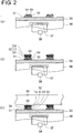
FIGs. 2(a) to 2(c) are (first) cross-sectional views for explaining the manufacturing process of the present invention. -
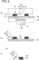
FIGs. 3(d) to 3(f) are (second) cross-sectional views for explaining the manufacturing process of the present invention. - An anisotropic conductive adhesive used in the present invention comprises a conductive paste, and contains an epoxy-modified silicone resin serving as a binder resin, a metal chelate serving as a latent curing agent, and a metal component serving as a conductive component. The anisotropic conductive adhesive does not contain flux.
- The epoxy-modified silicone resin serving as a binder resin is preferable due to its high viscosity stability and high thermal resistance. Examples of the epoxy-modified silicone resin used may include diglycidyl isocyanuryl-modified polysiloxanes represented by the following general formula (1).

- In the formula, R is an alkyl group such as a lower alkyl group having a carbon number of 1 to 6, or an aryl group such as a carbocyclic aromatic group and a heterocyclic aromatic group. Preferred concrete examples of the alkyl group may include a methyl group, an ethyl group, a propyl group, an isopropyl group, a butyl group, and an isobutyl group. A methyl group is particularly preferable as the alkyl group. Preferred concrete examples of the aryl group may include a phenyl group. n is a number of 1 to 40, is preferably a number of 1 to 9, and is more preferably a number of 1 or 2.
- The epoxy-modified silicone resin may contain a heterocyclic epoxy compound, an alicyclic epoxy compound, a hydrogenated epoxy compound, or the like within the range of not impairing the effects of the present invention, in addition to the diglycidyl isocyanuryl-modified polysiloxane represented by the general formula (1) .
- As the heterocyclic epoxy compound, there can be mentioned an epoxy compound having a triazine ring. Example thereof may include 1,3,5-tris(2,3-epoxypropyl)-1,3,5-triazine-2,4,6-(1H,3H,5H)-trione (in other words, triglycidyl isocyanurate).
- As the alicyclic epoxy compound, there can be preferably mentioned an alicyclic epoxy compound having two or more epoxy groups in a molecule. The alicyclic epoxy compound may be in a liquid form or a solid form. Specific examples thereof may include glycidyl hexahydrobisphenol A, and 3,4-epoxy cyclohexenyl methyl-3',4'-epoxy cyclohexene carboxylate. Among these, glycidyl hexahydrobisphenol A and 3,4-epoxy cyclohexenyl methyl-3',4'-epoxy cyclohexene carboxylate can preferably be used, because a cured product of the compound certainly has a light transmittance suited to mounting an LED element and the compound has an excellent rapid curing property.
- As the hydrogenated epoxy compound, hydrogenated products of the aforementioned heterocyclic epoxy compound and the alicyclic epoxy compound, and other well-known hydrogenated epoxy compounds can be used. The alicyclic epoxy compound, the heterocyclic epoxy compound, and the hydrogenated epoxy compound may each be used alone together with diglycidyl isocyanuryl-modified polysiloxane expressed by the general formula (1), or two or more types of these compounds may be used in combination. Another epoxy compound may be used together in addition to the epoxy compound(s) as long as the effects of the present invention are not impaired. Examples of the other epoxy compounds may include a glycidyl ether obtained by the reaction of epichlorohydrin with a polyhydric phenol, such as bisphenol A, bisphenol F, bisphenol S, tetramethyl bisphenol A, diaryl bisphenol A, hydroquinone, catechol, resorcin, cresol, tetrabromo bisphenol A, trihydroxybiphenyl, benzophenone, bis-resorcinol, bisphenol hexafluoroacetone, tetramethyl bisphenol A, tetramethyl bisphenol F, tris(hydroxyphenyl)methane, bixylenol, phenol novolac, and cresol novolac; a polyglycidyl ether obtained by the reaction of epichlorohydrin with an aliphatic polyhydric alcohol, such as glycerin, neopentyl glycol, ethylene glycol, propylene glycol, butylene glycol, hexylene glycol, polyethylene glycol, and polypropylene glycol; a glycidyl ether ester obtained by the reaction of epichlorohydrin with a hydroxycarboxylic acid, such as p-oxybenzoic acid and β-oxynaphthoic acid; a polyglycidyl ester obtained from a polycarboxylic acid, such as phthalic acid, methyl phthalic acid, isophtalic acid, terephthalic acid, tetrahydrophthalic acid, endomethylene tetrahydrophthalic acid, endomethylene hexahydrophthalic acid, trimellitic acid, and a polymerized fatty acid; a glycidyl amino glycidyl ether obtained from aminophenol and aminoalkyl phenol; a glycidyl amino glycidyl ester obtained from an aminobenzoic acid; a glycidyl amine obtained from such as aniline, toluidine, tribromoaniline, xylylenediamine, diaminocyclohexane, bis-aminomethyl cyclohexane, 4,4'-diaminodiphenyl methane, and 4,4'-diaminodiphenyl sulfone; and well-known epoxy compounds such as epoxy polyolefin.
- The central metal of the metal chelate compound is not specifically limited, and various metals such as aluminum, zirconium, and titanium can be used as the central metal. Among the metal chelates, an aluminum chelate having a high reactivity is preferably used in particular.
- As an aluminum chelate agent, there can be mentioned a complex compound in which three β-ketoenolate anions are coordinated to aluminum, as represented by the following general formula (2).

- In the formula, R1, R2, and R3 are each independently an alkyl group or an alkoxyl group. Examples of the alkyl group may include a methyl group, and an ethyl group. Examples of the alkoxyl group may include a methoxy group, an ethoxy group, and an oleyloxy group.
- Specific examples of the aluminum chelate agent represented by the general formula (2) may include aluminum tris(acetylacetonate), aluminum tris(ethylacetoacetate), aluminum mono acetylacetonate bis(ethylacetoacetate), aluminum mono acetylacetonate bis oleyl acetoacetate, ethylacetoacetate aluminum diisopropylate, and alkylacetoacetate aluminum diisopropylate.
- The metal chelate compound is desirably contained in the anisotropic conductive adhesive in a state of being impregnated into porous particles, and used as the latent curing agent. In addition to the metal chelate compound, a silane compound may be mixed as an auxiliary curing agent.
- The metal component serving as a conductive component is constituted of a metal powder. As the metal constituting the metal component, gold, silver, copper, nickel, metal-plated resin particles, and the like can be used.
- The metal powder preferably has a particle diameter of 3 µm or more and 10 µm or less as an average particle diameter from the viewpoint of ensuring application stability. The anisotropic conductive adhesive may contain a thermally-conductive filler. Examples of the thermally-conductive filler may include solder, lead-free solder, zinc oxide, boron nitride, and aluminum oxide. Among these, lead-free solder is desirable in terms of heat dissipation properties and cost.
- In the present invention, the mixing ratio (% by weight) between the epoxy-modified silicone resin and the metal chelate compound in the anisotropic conductive adhesive is preferably 100:2 to 100:10. The mixing ratio (% by volume) between the epoxy-modified silicone resin and the metal component is preferably 100:1 to 100:30. On the other hand, the mixing ratio (% by volume) between the epoxy-modified silicone resin and the thermally-conductive filler is preferably 100:1 to 100:30.
- First, as shown in
FIG. 1(a) , ceramic wiring boards 51 (each having a thickness of 0.4 mm) each of which has an aluminum (Al) wiring layer are disposed on astage 55. As shown inFIG. 1(b) , about 10 µg of an anisotropic conductive adhesive 50 is applied to the Al wiring layer of eachwiring board 51, so that the Al wiring layer of thewiring board 51 is brought into contact with the anisotropicconductive adhesive 50.FIG. 2(a) shows a cross-sectional view of such a state. In the drawing,reference numeral 54 denotes conductive particles, and the conductive particles here are metal-plated resin particles. The particle diameter of theconductive particles 54 is desirably 5 µm or more and 7 µm or less. In the drawing,reference numeral 59 denotes a thermally-conductive filler. The thermally-conductive filler here is constituted of lead-free solder particles having a particle diameter of 3 µm or more and 10 µm or less. - The
stage 55 is provided with aheating device 56. Apower supply 58 feeds an electric current to aheating element 57 provided in theheating device 56, and the temperature of thestage 55 has risen in advance to a certain temperature by heat generated by theheating element 57. Thestage 55 heated increases the temperatures of thewiring board 51 and the anisotropic conductive adhesive 50 disposed on thewiring board 51. - Next, as shown in
FIGs. 1(c) and2(b) , LED elements 52 (each having a size of 0.65 mm × 0.65 mm and a thickness of 0.36 mm) are disposed on the anisotropicconductive adhesive 50. In theLED element 52, afluorescent layer 16 is disposed on one surface of abody semiconductor chip 17, andelectrodes 61 are provided on the opposite surface thereof. TheLED element 52 is disposed such that theelectrodes 61 are in contact with the anisotropicconductive adhesive 50. - The
fluorescent layer 16 used here has a protective layer on the surface thereof, and as shown inFIGs. 1(d) and2(c) , apressing unit 53 provided in a pressure bonding device is brought into contact with the surface of thefluorescent layer 16 of theLED element 52. - The temperature of the
pressing unit 53 is controlled so as to be kept at the order of room temperature of 20°C or higher and 40°C or lower. The temperature of thestage 55 is controlled such that the temperature of thewiring board 51 is 160°C or higher and 210°C or lower, and preferably 180°C or higher and 190°C or lower. - When the
pressing unit 53 presses theLED element 52 in this state, the anisotropic conductive adhesive 50 is pushed to the outside of thewiring board 51 by a pressing force applied from thepressing unit 53 to theLED element 52. The distance between theLED element 52 and thewiring board 51 becomes short. As shown inFIG. 3(d) , theconductive particles 54 situated between the Al wiring layer of thewiring board 51 and theelectrodes 61 of theLED element 52 are in contact with both of the Al wiring layer of thewiring board 51 and theelectrodes 61, so that theelectrodes 61 are electrically connected to the Al wiring layer of thewiring board 51 through theconductive particles 54. - The anisotropic conductive adhesive 50 is primarily heated by the
heated wiring board 51, so that the temperature thereof is increased. Due to the temperature increase, the metal chelate compound contained in the anisotropic conductive adhesive 50 partly polymerizes the contained epoxy-modified silicone resin (diglycidyl isocyanuryl-modified polysiloxane). Then, theLED element 52 is bonded to thewiring board 51 by the compound obtained by the polymerization reaction. - The
fluorescent layer 16 of theLED element 52 has a property in which it collapses when heated to 190°C or higher. In this embodiment, since the temperature of thepressing unit 53 is set lower than that of thewiring board 51 having an upper limit temperature of 210°C. Thus, the temperature of the primarily-heatedLED element 52 that is sandwiched between thewiring board 51 and thepressing unit 53 is made lower than 210°C, i.e., the upper limit temperature of thewiring board 51. - Since the
fluorescent layer 16 tends to collapse when heated in a state of being pressed, a time for thepressing unit 53 to press theLED element 52 is set at 20 seconds or less, in order to prevent the collapse of thefluorescent layer 16. - When the press by the
pressing unit 53 has been completed after a lapse of the pressing time, as shown inFIG.3(e) , thepressing unit 53 moves away from theLED elements 52. In this state, theLED element 52 is bonded to thewiring board 51, and thus theLED element 52 and thewiring board 51 are temporarily connected so as not to move in a relative manner. - The
wiring board 51 and theLED element 52 temporarily connected thereto are conveyed into a heating oven while maintaining its temporarily connected state, to secondarily heat thewiring board 51, the anisotropic conductive adhesive 50, and theLED element 52. The temperature of the secondary heating by the heating oven is set lower than the temperature of the primary heating by theheating device 56 provided in thestage 55, and a heating time by the heating oven is set longer than the pressing time. - The secondary heating in the heating oven advances the polymerization reaction of the epoxy-modified silicone resin with the metal chelate compound. As a result, the anisotropic conductive adhesive 50 is cured and the
LED element 52 is fixed to thewiring board 51 as final connection. In this manner, thelight emitting device 10 as shown inFIG. 3(f) is obtained. - When the
light emitting device 10 is energized, thebody semiconductor chip 17 emits light. The wavelength of the radiated emission light is converted while passing through thefluorescent layer 16, and therefore white light is emitted from thelight emitting device 10. Note that, since the anisotropic conductive adhesive 50 according to this embodiment contains no flux, there is no need to provide a cleaning step for cleaning thelight emitting device 10. - In the manufacturing process of the
light emitting device 10, the temperature and pressing heating of thewiring board 51 were changed in the primary heating and theLED element 52 was pressed by thepressing unit 53, to thereby temporarily connect theLED element 52 to thewiring board 51 with the anisotropicconductive adhesive 50. At that time, the surface temperature of theLED element 52 on the side of thefluorescent layer 16 and the surface temperature of thewiring board 51 were measured. It is assumed that the temperature of theLED element 52 on the side of thefluorescent layer 16 is the same as the temperature of a surface of thepressing unit 53 that is brought into contact with theLED element 52. The conduction resistance between theLED element 52 and thewiring board 51 was measured, while applying a voltage to thewiring board 51, after removing thepressing unit 53 without heating by the heating oven. The following table 1 shows measurement results.[Table 1] Com. Ex. 1 Com. Ex. 2 Com. Ex. 3 Ex. 1 Ex. 2 Ex. 3 Ex. 4 Ex. 5 Ex. 6 Ex.7 Temperature Setting (°C) Fluorescent Side 160 180 190 35 35 35 35 35 35 35 Substrate Side 35 35 35 160 180 190 160 180 190 210 Pressing Time (sec) 60 60 60 60 60 60 20 20 20 20 Fluorescent Shape B C C B C C A A B C Temporal Connection C C C B B B B B B A Conduction Resistance C C C B A A B A A A - As for a conduction resistance, a resistance value was measured when a certain electric current was fed to each sample. "C" indicates a case where it is determined from the resistance value that no electrical connection is established. "A" indicates a case where the measured resistance value is equal to or less than a reference value. "B" indicates a case where although an electrical connection is established, the resistance value is more than the reference value.
- A force to remove the
LED element 52 from thewiring board 51 was also measured. "C" indicates a case where the polymerization of the anisotropic conductive adhesive 50 is insufficient and no temporal connection is achieved. "A" indicates a case where the temporal connection is achieved. "B" indicates a case where although the temporal connection is achieved, the removing force is less than a reference value. - In Table 1, the item of "fluorescent shape" indicates results of observing the shape of fluorescent particles in the
fluorescent layer 16 with a microscope, after removing thepressing unit 53. "C" indicates a case where the fluorescent particles are largely deformed in thefluorescent layer 16. "A" indicates a case where the fluorescent particles are hardly deformed in thefluorescent layer 16. "B" indicates a case where the deformation is in the middle of "C" and "A". Even when the item of "fluorescent shape" is evaluated as "C" or "B", the sample is encompassed by the present invention as long as thefluorescent layer 16 does not collapse and functions. - It is apparent from the results of Table 1 that a good electrical connection and a good temporal connection state are obtained, when the temperature of the
pressing unit 53 is 35°C or lower, and the temperature of thewiring board 51 is 160°C or higher and 210°C or lower, and the pressing time is 20 seconds or more and 60 seconds or less. -
- 10
- light emitting device
- 50
- anisotropic conductive adhesive
- 51
- wiring board
- 52
- LED element
- 53
- pressing unit
- 54
- conductive particle
- 55
- stage
- 56
- heating device
- 57
- heating element
- 58
- power supply
- 59
- thermally-conductive filler
- 61
- electrode
- 16
- fluorescent layer
- 17
- body semiconductor chip
Claims (4)
- A method for manufacturing a light emitting device, comprising:a disposition step of disposing an LED element on an anisotropic conductive adhesive, which contains a polymerization component and a curing agent and which is disposed on a wiring board;a primary heating step of increasing a temperature of the anisotropic conductive adhesive to cause a polymerization reaction of part of the polymerization component with the curing agent, while a pressing unit presses the LED element for a certain pressing time, to temporarily connect the LED element to the wiring board; anda secondary heating step of increasing temperatures of the wiring board, the anisotropic conductive adhesive, and the LED element, which are temporarily connected, to make final connection by the polymerization reaction of the polymerization component and curing of the anisotropic conductive adhesive, whereinthe LED element has a fluorescent layer,the polymerization component contains an epoxy-modified silicone resin,a metal chelate compound is used as the curing agent, andin the primary heating step, the wiring board is pressed at a temperature of 160°C or higher and 210°C or lower for the certain pressing time.
- The method for manufacturing a light emitting device according to claim 1, wherein the pressing time is 60 seconds or less.
- The method for manufacturing a light emitting device according to claim 1 or 2, wherein
the temperature of the wiring board is set lower in the secondary heating step than in the primary heating step, and
a heating time for heating the wiring board in the secondary heating step is set longer than the pressing time. - The method for manufacturing a light emitting device according to any one of claims 1 to 3, wherein a temperature of the pressing unit is kept at 20°C or higher and 40°C or lower.
Applications Claiming Priority (2)
| Application Number | Priority Date | Filing Date | Title |
|---|---|---|---|
| JP2015055406 | 2015-03-18 | ||
| PCT/JP2016/057527 WO2016148004A1 (en) | 2015-03-18 | 2016-03-10 | Method for manufacturing light emitting device |
Publications (3)
| Publication Number | Publication Date |
|---|---|
| EP3273493A1 true EP3273493A1 (en) | 2018-01-24 |
| EP3273493A4 EP3273493A4 (en) | 2018-10-10 |
| EP3273493B1 EP3273493B1 (en) | 2022-03-02 |
Family
ID=56919223
Family Applications (1)
| Application Number | Title | Priority Date | Filing Date |
|---|---|---|---|
| EP16764834.4A Active EP3273493B1 (en) | 2015-03-18 | 2016-03-10 | Method for manufacturing light emitting device |
Country Status (7)
| Country | Link |
|---|---|
| US (1) | US10626301B2 (en) |
| EP (1) | EP3273493B1 (en) |
| JP (1) | JP6565902B2 (en) |
| KR (1) | KR101985733B1 (en) |
| CN (1) | CN107408616A (en) |
| TW (1) | TWI700841B (en) |
| WO (1) | WO2016148004A1 (en) |
Families Citing this family (5)
| Publication number | Priority date | Publication date | Assignee | Title |
|---|---|---|---|---|
| JP2018088498A (en) * | 2016-11-29 | 2018-06-07 | デクセリアルズ株式会社 | Anisotropic conductive adhesive |
| KR102164171B1 (en) * | 2019-04-26 | 2020-10-13 | (주)엘프스 | self-assembled conductive bonding paste for mini LED chip bonding, mini LED chip-circuit board bondig module comprising the same and manufacturing method thereof |
| CN110289234B (en) * | 2019-07-04 | 2021-08-17 | 京东方科技集团股份有限公司 | Mass transfer method for light emitting cells, array substrate and display device |
| JP6691998B1 (en) | 2019-12-24 | 2020-05-13 | 株式会社鈴木 | Semiconductor device manufacturing method and semiconductor device manufacturing apparatus |
| JP2024035629A (en) * | 2022-09-02 | 2024-03-14 | 日亜化学工業株式会社 | Resin composition and light emitting device |
Family Cites Families (17)
| Publication number | Priority date | Publication date | Assignee | Title |
|---|---|---|---|---|
| CN100409423C (en) * | 2003-02-05 | 2008-08-06 | 千住金属工业株式会社 | Connection method between terminals and mounting method of semiconductor device |
| US20070000131A1 (en) * | 2005-05-04 | 2007-01-04 | Sonion Nederland Bv | Solid coated coil and a method of coating a coil |
| JP5499448B2 (en) | 2008-07-16 | 2014-05-21 | デクセリアルズ株式会社 | Anisotropic conductive adhesive |
| JP5476988B2 (en) * | 2009-12-30 | 2014-04-23 | デクセリアルズ株式会社 | Electrical device and epoxy resin composition used therefor |
| JP5402804B2 (en) * | 2010-04-12 | 2014-01-29 | デクセリアルズ株式会社 | Method for manufacturing light emitting device |
| JP5540916B2 (en) | 2010-06-15 | 2014-07-02 | デクセリアルズ株式会社 | Method for manufacturing connection structure |
| US8506105B2 (en) | 2010-08-25 | 2013-08-13 | Generla Electric Company | Thermal management systems for solid state lighting and other electronic systems |
| JP5609716B2 (en) | 2011-03-07 | 2014-10-22 | デクセリアルズ株式会社 | Light-reflective anisotropic conductive adhesive and light-emitting device |
| JP2012216712A (en) | 2011-03-28 | 2012-11-08 | Nitto Denko Corp | Method for manufacturing light-emitting diode device and light-emitting element |
| US20140023933A1 (en) * | 2011-03-30 | 2014-01-23 | Ohara Inc. | Non-aqueous electrolyte secondary battery, and process for producing same |
| JP2013179215A (en) * | 2012-02-29 | 2013-09-09 | Toyohashi Univ Of Technology | Led array and photoelectric integrated device |
| CN104487516B (en) * | 2012-07-19 | 2017-10-24 | 东丽株式会社 | Polysiloxane composition, electronic device and optics |
| JP6176910B2 (en) * | 2012-09-24 | 2017-08-09 | デクセリアルズ株式会社 | Method for manufacturing connection structure |
| JP2014141610A (en) * | 2013-01-25 | 2014-08-07 | Kyocera Chemical Corp | Thermosetting polysiloxane composition and method for manufacturing the same, polysiloxane premix, and electronic component |
| TW201431945A (en) * | 2013-01-31 | 2014-08-16 | 日本觸媒股份有限公司 | Curable resin composition and resin composition for optical semiconductor sealing |
| JP5985414B2 (en) | 2013-02-19 | 2016-09-06 | デクセリアルズ株式会社 | Anisotropic conductive adhesive, light emitting device, and method of manufacturing anisotropic conductive adhesive |
| WO2014132979A1 (en) * | 2013-02-27 | 2014-09-04 | 日亜化学工業株式会社 | Light emitting device, method for mounting light emitting element, and mounting device for light emitting elements |
-
2016
- 2016-03-10 EP EP16764834.4A patent/EP3273493B1/en active Active
- 2016-03-10 WO PCT/JP2016/057527 patent/WO2016148004A1/en not_active Ceased
- 2016-03-10 KR KR1020177022081A patent/KR101985733B1/en active Active
- 2016-03-10 JP JP2016513924A patent/JP6565902B2/en active Active
- 2016-03-10 US US15/550,544 patent/US10626301B2/en active Active
- 2016-03-10 CN CN201680013081.6A patent/CN107408616A/en active Pending
- 2016-03-16 TW TW105108060A patent/TWI700841B/en active
Also Published As
| Publication number | Publication date |
|---|---|
| WO2016148004A1 (en) | 2016-09-22 |
| JPWO2016148004A1 (en) | 2017-12-28 |
| JP6565902B2 (en) | 2019-08-28 |
| KR20170103897A (en) | 2017-09-13 |
| TWI700841B (en) | 2020-08-01 |
| KR101985733B1 (en) | 2019-06-04 |
| CN107408616A (en) | 2017-11-28 |
| US10626301B2 (en) | 2020-04-21 |
| EP3273493B1 (en) | 2022-03-02 |
| EP3273493A4 (en) | 2018-10-10 |
| US20180037773A1 (en) | 2018-02-08 |
| TW201705540A (en) | 2017-02-01 |
Similar Documents
| Publication | Publication Date | Title |
|---|---|---|
| EP3273493B1 (en) | Method for manufacturing light emitting device | |
| EP2899245A1 (en) | Anisotropic conductive adhesive | |
| EP2960312B1 (en) | Anisotropically conductive adhesive, light emitting device, and method for producing anisotropically conductive adhesive | |
| TWI597346B (en) | Anisotropic conductive adhesive and connecting structure | |
| KR101858758B1 (en) | Resin composition, resin composition sheet and method of manufacturing resin composition sheet, resin composition sheet with metal foil, b stage sheet, resin composition sheet with semi-cured metal foil, metal base wiring board material, metal base wiring board, led light source member, and power semiconductor device | |
| CN1220261C (en) | Electronic component | |
| EP3121237A1 (en) | Anisotropic conductive adhesive | |
| KR20150002805A (en) | Anisotropic conductive adhesive, method for manufacturing same, light emitting device, and method for manufacturing same | |
| JP2015088744A (en) | Light emitting device, anisotropic conductive adhesive, and method for manufacturing light-emitting device | |
| JP6802620B2 (en) | Manufacturing method of semiconductor light emitting device and semiconductor light emitting device | |
| KR102139124B1 (en) | Thermosetting resin composition, light-reflective anisotropic electroconductive adhesive, and light-emitting device | |
| JP2016201418A (en) | Adhesive film for joining semiconductor, and manufacturing method of semiconductor device | |
| CN1101594C (en) | Package body of semiconductor unit, its packaging method and packaging material thereof | |
| JP7200674B2 (en) | Manufacturing method of heat dissipation structure | |
| CN106459717B (en) | Adhesive and connection structure | |
| TWI669721B (en) | Anisotropic conductive adhesive | |
| JP2015220390A (en) | Method of manufacturing circuit board, circuit board, and electronic component mounting board | |
| JP2015026780A (en) | Insulating heat dissipating substrate | |
| JP5419948B2 (en) | Manufacturing method of resin-encapsulated semiconductor device | |
| US20150342052A1 (en) | Circuit substrate, electronic component mounting substrate and method for producing circuit substrate | |
| JP2015220389A (en) | Circuit board and electronic component mounting board |
Legal Events
| Date | Code | Title | Description |
|---|---|---|---|
| STAA | Information on the status of an ep patent application or granted ep patent |
Free format text: STATUS: THE INTERNATIONAL PUBLICATION HAS BEEN MADE |
|
| PUAI | Public reference made under article 153(3) epc to a published international application that has entered the european phase |
Free format text: ORIGINAL CODE: 0009012 |
|
| STAA | Information on the status of an ep patent application or granted ep patent |
Free format text: STATUS: REQUEST FOR EXAMINATION WAS MADE |
|
| 17P | Request for examination filed |
Effective date: 20170824 |
|
| AK | Designated contracting states |
Kind code of ref document: A1 Designated state(s): AL AT BE BG CH CY CZ DE DK EE ES FI FR GB GR HR HU IE IS IT LI LT LU LV MC MK MT NL NO PL PT RO RS SE SI SK SM TR |
|
| AX | Request for extension of the european patent |
Extension state: BA ME |
|
| DAV | Request for validation of the european patent (deleted) | ||
| DAX | Request for extension of the european patent (deleted) | ||
| A4 | Supplementary search report drawn up and despatched |
Effective date: 20180907 |
|
| RIC1 | Information provided on ipc code assigned before grant |
Ipc: C09J 183/04 20060101ALI20180903BHEP Ipc: H01L 33/62 20100101AFI20180903BHEP Ipc: C09J 9/02 20060101ALI20180903BHEP Ipc: C09J 11/06 20060101ALI20180903BHEP Ipc: C09J 5/06 20060101ALI20180903BHEP |
|
| GRAP | Despatch of communication of intention to grant a patent |
Free format text: ORIGINAL CODE: EPIDOSNIGR1 |
|
| STAA | Information on the status of an ep patent application or granted ep patent |
Free format text: STATUS: GRANT OF PATENT IS INTENDED |
|
| INTG | Intention to grant announced |
Effective date: 20211006 |
|
| GRAS | Grant fee paid |
Free format text: ORIGINAL CODE: EPIDOSNIGR3 |
|
| GRAA | (expected) grant |
Free format text: ORIGINAL CODE: 0009210 |
|
| STAA | Information on the status of an ep patent application or granted ep patent |
Free format text: STATUS: THE PATENT HAS BEEN GRANTED |
|
| AK | Designated contracting states |
Kind code of ref document: B1 Designated state(s): AL AT BE BG CH CY CZ DE DK EE ES FI FR GB GR HR HU IE IS IT LI LT LU LV MC MK MT NL NO PL PT RO RS SE SI SK SM TR |
|
| REG | Reference to a national code |
Ref country code: GB Ref legal event code: FG4D |
|
| REG | Reference to a national code |
Ref country code: CH Ref legal event code: EP Ref country code: AT Ref legal event code: REF Ref document number: 1472957 Country of ref document: AT Kind code of ref document: T Effective date: 20220315 |
|
| REG | Reference to a national code |
Ref country code: DE Ref legal event code: R096 Ref document number: 602016069608 Country of ref document: DE |
|
| REG | Reference to a national code |
Ref country code: IE Ref legal event code: FG4D |
|
| REG | Reference to a national code |
Ref country code: LT Ref legal event code: MG9D |
|
| REG | Reference to a national code |
Ref country code: NL Ref legal event code: MP Effective date: 20220302 |
|
| PG25 | Lapsed in a contracting state [announced via postgrant information from national office to epo] |
Ref country code: SE Free format text: LAPSE BECAUSE OF FAILURE TO SUBMIT A TRANSLATION OF THE DESCRIPTION OR TO PAY THE FEE WITHIN THE PRESCRIBED TIME-LIMIT Effective date: 20220302 Ref country code: RS Free format text: LAPSE BECAUSE OF FAILURE TO SUBMIT A TRANSLATION OF THE DESCRIPTION OR TO PAY THE FEE WITHIN THE PRESCRIBED TIME-LIMIT Effective date: 20220302 Ref country code: NO Free format text: LAPSE BECAUSE OF FAILURE TO SUBMIT A TRANSLATION OF THE DESCRIPTION OR TO PAY THE FEE WITHIN THE PRESCRIBED TIME-LIMIT Effective date: 20220602 Ref country code: LT Free format text: LAPSE BECAUSE OF FAILURE TO SUBMIT A TRANSLATION OF THE DESCRIPTION OR TO PAY THE FEE WITHIN THE PRESCRIBED TIME-LIMIT Effective date: 20220302 Ref country code: HR Free format text: LAPSE BECAUSE OF FAILURE TO SUBMIT A TRANSLATION OF THE DESCRIPTION OR TO PAY THE FEE WITHIN THE PRESCRIBED TIME-LIMIT Effective date: 20220302 Ref country code: ES Free format text: LAPSE BECAUSE OF FAILURE TO SUBMIT A TRANSLATION OF THE DESCRIPTION OR TO PAY THE FEE WITHIN THE PRESCRIBED TIME-LIMIT Effective date: 20220302 Ref country code: BG Free format text: LAPSE BECAUSE OF FAILURE TO SUBMIT A TRANSLATION OF THE DESCRIPTION OR TO PAY THE FEE WITHIN THE PRESCRIBED TIME-LIMIT Effective date: 20220602 |
|
| REG | Reference to a national code |
Ref country code: AT Ref legal event code: MK05 Ref document number: 1472957 Country of ref document: AT Kind code of ref document: T Effective date: 20220302 |
|
| PG25 | Lapsed in a contracting state [announced via postgrant information from national office to epo] |
Ref country code: PL Free format text: LAPSE BECAUSE OF FAILURE TO SUBMIT A TRANSLATION OF THE DESCRIPTION OR TO PAY THE FEE WITHIN THE PRESCRIBED TIME-LIMIT Effective date: 20220302 Ref country code: LV Free format text: LAPSE BECAUSE OF FAILURE TO SUBMIT A TRANSLATION OF THE DESCRIPTION OR TO PAY THE FEE WITHIN THE PRESCRIBED TIME-LIMIT Effective date: 20220302 Ref country code: GR Free format text: LAPSE BECAUSE OF FAILURE TO SUBMIT A TRANSLATION OF THE DESCRIPTION OR TO PAY THE FEE WITHIN THE PRESCRIBED TIME-LIMIT Effective date: 20220603 Ref country code: FI Free format text: LAPSE BECAUSE OF FAILURE TO SUBMIT A TRANSLATION OF THE DESCRIPTION OR TO PAY THE FEE WITHIN THE PRESCRIBED TIME-LIMIT Effective date: 20220302 |
|
| PG25 | Lapsed in a contracting state [announced via postgrant information from national office to epo] |
Ref country code: NL Free format text: LAPSE BECAUSE OF FAILURE TO SUBMIT A TRANSLATION OF THE DESCRIPTION OR TO PAY THE FEE WITHIN THE PRESCRIBED TIME-LIMIT Effective date: 20220302 |
|
| PG25 | Lapsed in a contracting state [announced via postgrant information from national office to epo] |
Ref country code: SM Free format text: LAPSE BECAUSE OF FAILURE TO SUBMIT A TRANSLATION OF THE DESCRIPTION OR TO PAY THE FEE WITHIN THE PRESCRIBED TIME-LIMIT Effective date: 20220302 Ref country code: SK Free format text: LAPSE BECAUSE OF FAILURE TO SUBMIT A TRANSLATION OF THE DESCRIPTION OR TO PAY THE FEE WITHIN THE PRESCRIBED TIME-LIMIT Effective date: 20220302 Ref country code: RO Free format text: LAPSE BECAUSE OF FAILURE TO SUBMIT A TRANSLATION OF THE DESCRIPTION OR TO PAY THE FEE WITHIN THE PRESCRIBED TIME-LIMIT Effective date: 20220302 Ref country code: PT Free format text: LAPSE BECAUSE OF FAILURE TO SUBMIT A TRANSLATION OF THE DESCRIPTION OR TO PAY THE FEE WITHIN THE PRESCRIBED TIME-LIMIT Effective date: 20220704 Ref country code: EE Free format text: LAPSE BECAUSE OF FAILURE TO SUBMIT A TRANSLATION OF THE DESCRIPTION OR TO PAY THE FEE WITHIN THE PRESCRIBED TIME-LIMIT Effective date: 20220302 Ref country code: CZ Free format text: LAPSE BECAUSE OF FAILURE TO SUBMIT A TRANSLATION OF THE DESCRIPTION OR TO PAY THE FEE WITHIN THE PRESCRIBED TIME-LIMIT Effective date: 20220302 Ref country code: AT Free format text: LAPSE BECAUSE OF FAILURE TO SUBMIT A TRANSLATION OF THE DESCRIPTION OR TO PAY THE FEE WITHIN THE PRESCRIBED TIME-LIMIT Effective date: 20220302 |
|
| REG | Reference to a national code |
Ref country code: CH Ref legal event code: PL |
|
| PG25 | Lapsed in a contracting state [announced via postgrant information from national office to epo] |
Ref country code: IS Free format text: LAPSE BECAUSE OF FAILURE TO SUBMIT A TRANSLATION OF THE DESCRIPTION OR TO PAY THE FEE WITHIN THE PRESCRIBED TIME-LIMIT Effective date: 20220702 Ref country code: AL Free format text: LAPSE BECAUSE OF FAILURE TO SUBMIT A TRANSLATION OF THE DESCRIPTION OR TO PAY THE FEE WITHIN THE PRESCRIBED TIME-LIMIT Effective date: 20220302 |
|
| REG | Reference to a national code |
Ref country code: DE Ref legal event code: R097 Ref document number: 602016069608 Country of ref document: DE |
|
| REG | Reference to a national code |
Ref country code: BE Ref legal event code: MM Effective date: 20220331 |
|
| PLBE | No opposition filed within time limit |
Free format text: ORIGINAL CODE: 0009261 |
|
| STAA | Information on the status of an ep patent application or granted ep patent |
Free format text: STATUS: NO OPPOSITION FILED WITHIN TIME LIMIT |
|
| PG25 | Lapsed in a contracting state [announced via postgrant information from national office to epo] |
Ref country code: MC Free format text: LAPSE BECAUSE OF FAILURE TO SUBMIT A TRANSLATION OF THE DESCRIPTION OR TO PAY THE FEE WITHIN THE PRESCRIBED TIME-LIMIT Effective date: 20220302 Ref country code: LU Free format text: LAPSE BECAUSE OF NON-PAYMENT OF DUE FEES Effective date: 20220310 Ref country code: LI Free format text: LAPSE BECAUSE OF NON-PAYMENT OF DUE FEES Effective date: 20220331 Ref country code: IE Free format text: LAPSE BECAUSE OF NON-PAYMENT OF DUE FEES Effective date: 20220310 Ref country code: FR Free format text: LAPSE BECAUSE OF NON-PAYMENT OF DUE FEES Effective date: 20220502 Ref country code: DK Free format text: LAPSE BECAUSE OF FAILURE TO SUBMIT A TRANSLATION OF THE DESCRIPTION OR TO PAY THE FEE WITHIN THE PRESCRIBED TIME-LIMIT Effective date: 20220302 Ref country code: CH Free format text: LAPSE BECAUSE OF NON-PAYMENT OF DUE FEES Effective date: 20220331 |
|
| 26N | No opposition filed |
Effective date: 20221205 |
|
| PG25 | Lapsed in a contracting state [announced via postgrant information from national office to epo] |
Ref country code: SI Free format text: LAPSE BECAUSE OF FAILURE TO SUBMIT A TRANSLATION OF THE DESCRIPTION OR TO PAY THE FEE WITHIN THE PRESCRIBED TIME-LIMIT Effective date: 20220302 Ref country code: BE Free format text: LAPSE BECAUSE OF NON-PAYMENT OF DUE FEES Effective date: 20220331 |
|
| GBPC | Gb: european patent ceased through non-payment of renewal fee |
Effective date: 20220602 |
|
| PG25 | Lapsed in a contracting state [announced via postgrant information from national office to epo] |
Ref country code: GB Free format text: LAPSE BECAUSE OF NON-PAYMENT OF DUE FEES Effective date: 20220602 |
|
| PG25 | Lapsed in a contracting state [announced via postgrant information from national office to epo] |
Ref country code: IT Free format text: LAPSE BECAUSE OF FAILURE TO SUBMIT A TRANSLATION OF THE DESCRIPTION OR TO PAY THE FEE WITHIN THE PRESCRIBED TIME-LIMIT Effective date: 20220302 |
|
| PG25 | Lapsed in a contracting state [announced via postgrant information from national office to epo] |
Ref country code: HU Free format text: LAPSE BECAUSE OF FAILURE TO SUBMIT A TRANSLATION OF THE DESCRIPTION OR TO PAY THE FEE WITHIN THE PRESCRIBED TIME-LIMIT; INVALID AB INITIO Effective date: 20160310 |
|
| PG25 | Lapsed in a contracting state [announced via postgrant information from national office to epo] |
Ref country code: MK Free format text: LAPSE BECAUSE OF FAILURE TO SUBMIT A TRANSLATION OF THE DESCRIPTION OR TO PAY THE FEE WITHIN THE PRESCRIBED TIME-LIMIT Effective date: 20220302 Ref country code: CY Free format text: LAPSE BECAUSE OF FAILURE TO SUBMIT A TRANSLATION OF THE DESCRIPTION OR TO PAY THE FEE WITHIN THE PRESCRIBED TIME-LIMIT Effective date: 20220302 |
|
| PG25 | Lapsed in a contracting state [announced via postgrant information from national office to epo] |
Ref country code: TR Free format text: LAPSE BECAUSE OF FAILURE TO SUBMIT A TRANSLATION OF THE DESCRIPTION OR TO PAY THE FEE WITHIN THE PRESCRIBED TIME-LIMIT Effective date: 20220302 |
|
| PG25 | Lapsed in a contracting state [announced via postgrant information from national office to epo] |
Ref country code: MT Free format text: LAPSE BECAUSE OF FAILURE TO SUBMIT A TRANSLATION OF THE DESCRIPTION OR TO PAY THE FEE WITHIN THE PRESCRIBED TIME-LIMIT Effective date: 20220302 |
|
| REG | Reference to a national code |
Ref country code: DE Ref legal event code: R079 Ref document number: 602016069608 Country of ref document: DE Free format text: PREVIOUS MAIN CLASS: H01L0033620000 Ipc: H10H0020857000 |
|
| PGFP | Annual fee paid to national office [announced via postgrant information from national office to epo] |
Ref country code: DE Payment date: 20260128 Year of fee payment: 11 |