EP3273390A2 - Hardware-implementierung eines temporären speichersystems - Google Patents
Hardware-implementierung eines temporären speichersystems Download PDFInfo
- Publication number
- EP3273390A2 EP3273390A2 EP17181762.0A EP17181762A EP3273390A2 EP 3273390 A2 EP3273390 A2 EP 3273390A2 EP 17181762 A EP17181762 A EP 17181762A EP 3273390 A2 EP3273390 A2 EP 3273390A2
- Authority
- EP
- European Patent Office
- Prior art keywords
- representation
- input
- array
- scalar value
- frame
- Prior art date
- Legal status (The legal status is an assumption and is not a legal conclusion. Google has not performed a legal analysis and makes no representation as to the accuracy of the status listed.)
- Granted
Links
Images




Classifications
-
- G—PHYSICS
- G06—COMPUTING OR CALCULATING; COUNTING
- G06N—COMPUTING ARRANGEMENTS BASED ON SPECIFIC COMPUTATIONAL MODELS
- G06N3/00—Computing arrangements based on biological models
- G06N3/02—Neural networks
- G06N3/06—Physical realisation, i.e. hardware implementation of neural networks, neurons or parts of neurons
- G06N3/063—Physical realisation, i.e. hardware implementation of neural networks, neurons or parts of neurons using electronic means
-
- G—PHYSICS
- G06—COMPUTING OR CALCULATING; COUNTING
- G06N—COMPUTING ARRANGEMENTS BASED ON SPECIFIC COMPUTATIONAL MODELS
- G06N3/00—Computing arrangements based on biological models
- G06N3/02—Neural networks
- G06N3/04—Architecture, e.g. interconnection topology
- G06N3/049—Temporal neural networks, e.g. delay elements, oscillating neurons or pulsed inputs
-
- G—PHYSICS
- G06—COMPUTING OR CALCULATING; COUNTING
- G06F—ELECTRIC DIGITAL DATA PROCESSING
- G06F12/00—Accessing, addressing or allocating within memory systems or architectures
- G06F12/02—Addressing or allocation; Relocation
- G06F12/0207—Addressing or allocation; Relocation with multidimensional access, e.g. row/column, matrix
-
- G—PHYSICS
- G06—COMPUTING OR CALCULATING; COUNTING
- G06N—COMPUTING ARRANGEMENTS BASED ON SPECIFIC COMPUTATIONAL MODELS
- G06N3/00—Computing arrangements based on biological models
- G06N3/02—Neural networks
- G06N3/04—Architecture, e.g. interconnection topology
- G06N3/044—Recurrent networks, e.g. Hopfield networks
-
- G—PHYSICS
- G06—COMPUTING OR CALCULATING; COUNTING
- G06N—COMPUTING ARRANGEMENTS BASED ON SPECIFIC COMPUTATIONAL MODELS
- G06N3/00—Computing arrangements based on biological models
- G06N3/02—Neural networks
- G06N3/04—Architecture, e.g. interconnection topology
- G06N3/047—Probabilistic or stochastic networks
-
- G—PHYSICS
- G06—COMPUTING OR CALCULATING; COUNTING
- G06N—COMPUTING ARRANGEMENTS BASED ON SPECIFIC COMPUTATIONAL MODELS
- G06N3/00—Computing arrangements based on biological models
- G06N3/02—Neural networks
- G06N3/04—Architecture, e.g. interconnection topology
- G06N3/0495—Quantised networks; Sparse networks; Compressed networks
-
- G—PHYSICS
- G06—COMPUTING OR CALCULATING; COUNTING
- G06N—COMPUTING ARRANGEMENTS BASED ON SPECIFIC COMPUTATIONAL MODELS
- G06N3/00—Computing arrangements based on biological models
- G06N3/02—Neural networks
- G06N3/06—Physical realisation, i.e. hardware implementation of neural networks, neurons or parts of neurons
- G06N3/063—Physical realisation, i.e. hardware implementation of neural networks, neurons or parts of neurons using electronic means
- G06N3/065—Analogue means
-
- G—PHYSICS
- G06—COMPUTING OR CALCULATING; COUNTING
- G06F—ELECTRIC DIGITAL DATA PROCESSING
- G06F2212/00—Indexing scheme relating to accessing, addressing or allocation within memory systems or architectures
- G06F2212/10—Providing a specific technical effect
- G06F2212/1016—Performance improvement
-
- G—PHYSICS
- G06—COMPUTING OR CALCULATING; COUNTING
- G06N—COMPUTING ARRANGEMENTS BASED ON SPECIFIC COMPUTATIONAL MODELS
- G06N3/00—Computing arrangements based on biological models
- G06N3/02—Neural networks
- G06N3/04—Architecture, e.g. interconnection topology
- G06N3/045—Combinations of networks
Definitions
- the present invention relates to the field of temporal memory systems, namely memory systems which enable pattern identification and prediction, based on a streaming input that is fed to them in a continuous way.
- the present invention relates to learning algorithms needed to train a temporal memory with a continuous stream of input data.
- non-volatile memory (NVM) elements may be used as building blocks of such temporal memory systems.
- branch predictors are naive versions of temporal memories, given that they enable prediction of a branch instruction outcome.
- hierarchical branch predictors the prediction correctness is compared between different predictors and the most successful one is used to create a prediction about the handled branch instruction outcome.
- a temporal memory is a system that identifies and predicts input data, based on the sequence of data that has been submitted to it up to a specific point in time. Naturally, certain sequences of input favour specific predictions or lead to the detection of specific patterns in the streaming input of the temporal memory.
- HTM hierarchical temporal memories
- Numenta has additionally disclosed the principles of the cortical learning algorithm (CLA), which is used to train the hierarchical temporal memory with a continuous stream of input data.
- CLA cortical learning algorithm
- the CLA consists of two parts: a spatial pooler that converts sensory input data into a sparse bit representation, and a temporal pooler that can learn and predict sequences of data using the sparse bit representation.
- the software version of Numenta's HTM is publicly available (https://github.com/numenta/nupic). Hardware implementations of the HTM concept have also been attempted. Most notably, work by UIUC attempts to use spatial and temporal pooler concepts described above with a combination of NVM elements (http://dx.doi.org/10.1109/TNNLS.2015.2462731). Even though temporal grouping of spatially pooled inputs is enabled using the hardware implementation detailed in the UIUC paper, there is no aspect of time series prediction, based on the inputs provided to the HTM.
- the current disclosure describes a device and system that uses memory cells, for instance, but not limited thereto, NVM memory cells, each memory cell comprising at least one memory cell element, to enable pattern identification and prediction, based on a sequence of input frames that have been fed to the system.
- memory cells for instance, but not limited thereto, NVM memory cells, each memory cell comprising at least one memory cell element, to enable pattern identification and prediction, based on a sequence of input frames that have been fed to the system.
- the present invention provides a hardware implementation of a temporal memory system.
- the hardware implementation comprises
- temporal memory system hardcodes in its memory cells the likelihood of occurrence of sequences of abstract symbols.
- the scalar values stored in the memory cells express the likelihood of temporal coincidence between a currently observed frame (N) and a previously observed frame (N-k), where k ⁇ 1.
- a specified time in the past is corresponding to a predetermined number of frames before a current input frame.
- the hardware implementation may furthermore comprise a buffering unit for implementing a first-in-first-out (FIFO) queue with a pre-determined depth for storing a given number of representations of previous input frames.
- the representation of the previous input frames may be obtained from reading out the array of memory cells.
- the FIFO may be adapted for holding a sequence of consecutive previously read out sparsified representations of input frames.
- the first-in-first-out (FIFO) queue may furthermore comprise a shifting unit, adapted for enqueuing a row address to the FIFO. This allows to fill the FIFO with relevant data, to be used during processing of transitions of frames, or during prediction of occurrence of a next frame.
- the reading unit may comprise a selection unit for selecting a scalar value based on a criterion, and its corresponding addresses.
- the at least one array may be a square array.
- the memory cells may be adapted for supporting three operations: read scalar value, increment scalar value, for instance by a set operation on a RRAM element, and decrement scalar value, for instance by a reset operation on a RRAM element.
- the addressing unit may be adapted for identifying one or more memory cells in the at least one array prior to implementing any of a read operation, an increment operation or a decrement operation.
- the input system may comprise a block-level input unit adapted for receiving partitioned input from an input unit, and for transforming this partitioned input into a representation fit for memory cell addressing in the at least one array.
- the input representation corresponds to the dimensions of the at least one array.
- the memory cells may include non-volatile memory cells.
- each memory cell or the at least one array includes one or more of any of RRAM cells, e.g. stochastical RRAM (resistive random-access memory) cells, filamentary RRAM cells, OXRAM (oxide-based resistive memory RAM) cells, CBRAM (conductive bridging RAM) cells, VMCO (vacancy-modulated conductive oxide) RAM cells, PMC cells (programmable metallization cells); PCM (phase-change memory) cells; SRAM (static random-access memory) cells; flash cells; floating gate cells; or MRAM (magnetoresistive random-access memory) cells, such as for instance STT (spin-transfer torque) MRAM cells or SOT (spin orbit torque) MRAM cells, SONOS (silicon-oxide-nitride-oxide-silicon) cells.
- RRAM cells e.g. stochastical RRAM (resistive random-access memory) cells, filamentary RRAM cells, OXRAM (oxide
- filamentary RRAM cells are particularly advantageous.
- the working principle of filamentary RRAM cells includes growing and shrinking a narrow conductive filament by applying a voltage of different polarity and magnitude. This growing and shrinking of the conductive filament may mimic growth and removal of synaptic connections in a biological brain.
- the use of filamentary RRAM allows for a single chip solution rather than a full computer with extended memory which is needed to mimic the brain-inspired operation through software. OxRAM cells are particularly useful because they can reinforce the filament generation.
- the memory cells may include volatile memory cells, such as for instance DRAM cells.
- the memory cells may be of the type single selector, single storage element.
- a 1Transistor-1Resistor (1T1R) implementation of a memory cell with RRAM memory elements is well-known in the art.
- a 1T1R Xbar can be implemented. In such implementation, the context of a learned sequence is converted into a 2D pattern of filament connections in a 2D crossbar cell array.
- the present invention provides a method for processing the transition of a first frame to a second frame in a system comprising at least one array of memory cells logically organized in rows and columns. Each memory cell is adapted for storing a scalar value and for changing, e.g. incrementing or decrementing, the stored scalar value.
- the method comprises:
- a method according to embodiments of the present invention may furthermore comprise signalling an anomaly event if none of the read memory cells satisfies the selection criterion at step (c).
- reading a memory cell may include reading a scalar value stored in the memory cell, and identifying a memory cell that satisfies the selection criterion may include testing the read scalar value. Testing the read scalar values may for instance be done via comparison with a threshold on current or resistance or voltage.
- the representation of the first frame may be a sparse data bit string comprising only one logically high bit or only one logically low bit.
- the present invention provides a method for predicting a representation of a next frame based on a current frame in a system comprising at least one array of memory cells logically organized in rows and columns. Each memory cell is adapted for storing a scalar value and for changing, e.g. incrementing or decrementing, the stored scalar value.
- the method comprises:
- a method according to the third aspect of the present invention may furthermore comprise
- the present invention provides the use of at least one array of memory cells logically organized in rows and columns, for implementing a hardware implementation of a temporal memory system for processing or predicting the transition of a first frame to a second frame.
- Each memory cell in the array is adapted for storing a scalar value and for changing, e.g. incrementing and/or decrementing, the stored scalar value, the scalar value corresponding to a likelihood of temporal coincidence between a input representation of the first frame applied as a row address to the array, and the column address, this likelihood being adjustable through the scalar value stored in the memory cell.
- an input representation of the second frame may be applied as a column address to the array, wherein an increment or decrement operation is applied to the scalar value of a memory cell each time it is addressed by a row address and a column address.
- row addresses and column addresses may be sparse bit strings, for instance comprising only one logically high bit or only one logically low bit.
- a hardware implementation of a temporal memory system comprises at least one array of memory cells, each memory cell comprising at least one memory cell element.
- the memory cells may be, but do not need to be, non-volatile memory cells, comprising non-volatile memory cell elements.
- memory cells may comprise or consist of one or more volatile memory cell elements.
- the memory cell elements may be RRAM (Resistive Random Access Memory) elements.
- RRAM technology has been developed as an alternative memory technology.
- One particular type of RRAM which may be used in embodiments of the present invention is filamentary RRAM, that consists of growing and shrinking a narrow conductive filament by applying voltages of different polarity and magnitude.
- Embodiments of the present invention may use oxygen vacancy-based RRAM (OXRRAM; RRAM with conductive filament made of oxygen vacancies), but metal ion-based filamentary RRAM (Conductive Bridge RAM or CBRAM; with filament in metal ions), VMCO (Vacancy-modulated conductive oxide Resistive Ram) or PCM (Phase-Change Memory) could also be applied in a very similar way.
- OXRRAM oxygen vacancy-based RRAM
- CBRAM Conductive Bridge RAM or CBRAM
- VMCO Vacancy-modulated conductive oxide Resistive Ram
- PCM Phase-Change Memory
- MRAM Magneticoresistive Random-Access Memory
- STT MRAM Spin-Transfer Torque Magnetic RAM
- SOT MRAM Spin Orbit Torque Magnetic RAM
- SRAM Statistic Random-Access Memory
- FLASH or floating gate memory devices can be used as memory cell elements.
- SONOS Silicon-Oxide-Nitride-Oxide-Silicon
- DRAM Dynamic Random-Access Memory
- the memory cells are probabilistic devices. This means that when given a stimulus, e.g. a pulse with length t seconds and V amplitude, the response will be probabilistic, i.e. there are multiple possible outcomes, each having varying degrees of certainty of occurrence.
- a stimulus e.g. a pulse with length t seconds and V amplitude
- the response will be probabilistic, i.e. there are multiple possible outcomes, each having varying degrees of certainty of occurrence.
- stimuli e.g. voltage and time thereof, can be chosen such that the probability for getting to an ON state is pre-determined.
- the memory cells are said to be “logically organised in rows and columns” in an array.
- the terms “horizontal” and “vertical” (related to the terms “row” and “column”, respectively) are used to provide a co-ordinate system and for ease of explanation only. They do not need to, but may, refer to an actual physical direction of the device.
- the terms “column” and “row” are used to describe sets of array elements which are linked together.
- the linking can be in the form of a Cartesian array of rows and columns; however, the present invention is not limited thereto. As will be understood by those skilled in the art, columns and rows can be easily interchanged and it is intended in this disclosure that these terms be interchangeable.
- non-Cartesian arrays may be constructed and are included within the scope of the invention. Accordingly the terms “row” and “column” should be interpreted widely. To facilitate in this wide interpretation, the claims refer to logically organised in rows and columns. By this is meant that sets of memory cells, e.g. RRAM cells, are linked together in a topologically linear intersecting manner; however, that the physical or topographical arrangement need not be so.
- the rows may be circles and the columns radii of these circles and the circles and radii are described in this invention as "logically organised" in rows and columns. It should be understood that this terminology is used only to facilitate a better understanding of the specific structure being described, and is in no way intended to limit the invention.
- a “scalar value” in the context of the present invention is a single value, as opposed to a data structure, like a vector or a matrix which contain a plurality of values.
- the scalar value can be binary (only two levels: “logical high” or "logical low"), or it can be a multi-level. If the scalar value is of a multi-level type, each of the levels is distinguishable from the others.
- Sparse data in the context of the present invention is data with a limited number of digits of a particular value.
- sparse data may for instance have only one or only a few "1" (logically high) bits, where data processing is based on these "1" bits.
- This is not limiting to the present invention, and in alternative embodiments inverse implementations could be provided, where data only has one or a few "0" (logically low) bits, and where the further processing is done on the "0" bits.
- the sparse data only contains a limited amount of "1" bits, this way of explaining not being intended to be limiting for the present invention.
- the temporal memory system 10 is the general purpose building block of the present invention. It gets a streaming input of data that can come from any source.
- the streaming input of data consists of a sequence of frames, each partition of the streaming input referred to as a single frame (thus, the stream comprising a temporal sequence of frames).
- the temporal memory system 10 learns transitions of frames in a sequence in a context of a continuous stream of such frames. It is an object of embodiments of the present invention to predict what frame is most likely to appear in the input stream of the system. It is an advantage of embodiments of the present invention that this can be done at reduced power consumption.
- the temporal memory system 10 comprises at least one array of memory cells, for instance, but not limited thereto, non-volatile memory cells, each memory cell comprising at least one memory cell element.
- memory cells can contain a plurality of, e.g. two or more, memory cell elements.
- the implementation of the temporal memory system 10 can be very different, depending on the type of memory cells and memory cell elements used.
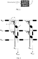
- the implementation in RRAM technology may comprise a 1-transistor -1-resistor type crossbar array as laid out schematically in FIG. 2 .
- the array may be a square array, for instance an array of (LxM) 2 memory cells, where M and L are defined in the DETAILED DESCRIPTION and OPERATIONAL DESCRIPTION parts of the current disclosure.
- FIG. 2 illustrates part of an array of memory cells, in particular it illustrates four memory cells 40.
- Each illustrated memory cell 40 comprises a selector element 20 and a storage element or memory cell element 21.
- the memory cells 40 are logically organised in rows and columns.
- the array is provided with row lines and with column lines. In the embodiment illustrated, the array is provided with one row line per row, and two column lines per column.
- the row lines are row addressing lines for addressing memory cells in a row.
- One set of column lines are column addressing lines, for addressing memory cells in a column.
- the other set of column lines are output lines, for allowing readout content of memory cells addressed by means of the row addressing lines and column addressing lines.
- the temporal memory is implemented by making a crossbar array of memory cell elements, e.g. filamentary RRAM elements.
- the array contains, in the memory cell elements, stored information about the strength of connection between rows and columns.
- an interconnect matrix is provided, where the interconnections are formed by the memory cells.
- the connectivity is stored in the memory cell elements.
- the hardware implementation if looked at from a higher level, comprises at least one array of memory cells, in which memory cell elements store connectivity information between two frames (i.e. the chance that a first frame goes over into a second frame) as a likelihood value, which can, for instance, be the strength of the connection, or the time duration a connection lasts.
- this invention proposes the use of registers and basic logic functions to orchestrate the operation of this temporal memory system, e.g. non-volatile temporal memory system.
- this temporal memory system e.g. non-volatile temporal memory system.
- information is sparsely stored.
- the proposed logic enables use of the array of memory cells for training and prediction. The exact way of driving row addressing lines, column addressing lines and output lines in the array of memory cells is described below.
- FIG. 3 gives a schematic overview of a hardware implementation of a temporal memory system 10, according to embodiments of the present invention.
- the hardware implementation comprises a plurality of sub-systems 30, 31, 32, further called blocks.
- the hardware implementation is suitable and adapted for handling a stream or sequence of input frames 33, and for predicting therefrom future input frames. In accordance with embodiments of the present invention, this is enabled by partitioning and quantizing the input frame into block-level inputs, which are then processed individually and in parallel to produce block-level predictions.
- An input frame 33 is an arbitrary data structure (e.g. a bundle of signal values, image frames, sensor data, etc.), instances of which are fed to the system 10 (and are processed) in a streaming fashion (the one after the other).
- the goal of a temporal memory system 10 according to embodiments of the present invention is to be able to produce predictions about future frames.
- an input unit 34 is provided.
- the input unit 34 is adapted for receiving input data (an input frame 33) from a data stream (sequence of input frames), and for creating a representation therefor.
- the representation of the input data is a sequence of logical high and low values (e.g. 0 and 1).
- the input unit 34 partitions the representation of the input frame 33 and quantizes the information contained in each partition.
- the result of this process is a bundle of block-level inputs 350, 351, 352, each one submitted to each block 30, 31, 32 of the system 10 for future processing.
- a block-level input 350, 351, 352 is a result of quantizing a subset of the information found in the representation of the input frame 33. It is a bit string with M bits, only 1 of which is being equal to 1.
- the blocks 30, 31, 32 of the system 10 each comprise a memory cell array 360, 361, 362, with supporting circuitry to orchestrate their access and read/write patterns so that a block-level prediction can be produced.
- the supporting circuitry may comprise a block-level input unit, row and column addressing circuitry, a reading unit, a delay element and storage means for storing prediction data, as illustrated in more detail in FIG. 9 .
- Blocks 30, 31, 32 operate fully independently and in parallel, so in the remainder of the disclosure the structure and operation of only a single block (for the sake of brevity) will be dealt with, the structure and operation of the blocks 30, 31, 32 being similar.
- K blocks may for instance be up to 1024 blocks, or even higher, depending on the application.
- FIG. 4 gives a schematic overview of a block of the hardware implementation of a temporal memory system 10 as illustrated in FIG. 3 ; for instance FIG. 4 shows block 30.
- a single block of the system 10 performs all the learning and prediction operations independently of all other blocks, based on block-level input that originates from the input frame 33 to the entire system 10, and is only a part of the representation thereof.
- Block 30 comprises an array 360 of memory cells 40, logically organized in rows and columns.
- Each memory cell 40 more particularly the at least one memory cell element thereof, for instance memory cell element 21 as illustrated in FIG. 2 , is adapted for storing a scalar value and for changing, for instance incrementing or decrementing, the stored scalar value.
- the memory cells 40 more particularly the memory cell elements, should thus be changeable, e.g. it should be incrementable.
- the incrementation may be done in any suitable way, for instance in a linear way, a logarithmic way, an exponential way.
- the memory cell elements are thus multi-level storage devices, including but not limited to binary storage devices.
- the memory cell elements may be stable non-volatile memory elements; which keep their content for a predefined time, whereby the time of stability is determined depending on the applications where the array is used.
- the memory cell elements are symmetrical in reading and writing.
- the memory cell elements may for instance be filamentary RRAM elements, of which a resistance value can be read.
- Embodiments of the present invention may use oxygen vacancy-based RRAM (OXRRAM; RRAM with conductive filament made of oxygen vacancies), or metal ion-based filamentary RRAM (Conductive Bridge RAM; with filament in metal ions).
- OXRRAM oxygen vacancy-based RRAM
- metal ion-based filamentary RRAM Conductive Bridge RAM; with filament in metal ions.
- the present invention is, however, not limited thereto.
- the memory cell elements may be STT MRAM device, of which resistance may be read, according to the magnetization direction of the MRAM device. Other examples are given higher up, and are not repeated here for sake of brevity.
- the block 30 of the hardware implementation of the temporal memory system 10 further comprises an addressing unit for identifying a memory cell 40 in the array 360 with a row address and a column address.
- the addressing unit comprises a column addressing unit 41 and a row addressing unit 42.
- the block-level input 350 received from the input unit 34 is a bit string of length M, comprising bit-values "0" (logical low) and "1" (logical high), with only a single "1" (logical high). This typically corresponds to one-hot encoding of the quantized information that has come from the input frame 33 through the partitioning and quantization step in the input unit 34. Based on the block-level input 350, there are two derivative representations of this block-level input 350:
- the column addressing unit 41 is adapted for receiving the partitioned and quantized representation of current input data, i.e. the M-bits block-level input 350, and for generating the derivative representation thereof.
- the columns addressing unit 41 may be adapted for receiving such derivative representation from a block-level input unit 91.
- the block-level input unit 91 is adapted for receiving the partitioned and quantized representation of current input data, i.e. the M-bits block-level input 350, and for generating the derivative representation thereof.
- the block-level input unit 91 together with the input unit 34 may form an input system 340 for receiving an input frame as input and creating a representation for that input, which is fit for memory cell addressing in the at least one array.
- the column addressing unit 41 is adapted for applying the MxL-bit long derivative representation of current input data as a column address to the array 360 of memory cells 40.
- the row addressing unit 42 is adapted for receiving the representation of input data from a frame at a specified time in the past, and for applying this representation of past input data as a row address to the array 360 of memory cells 40.
- the representation of the past input data may preferably be a winning representation, i.e. with only one "1" (logically high).
- a reading unit 43 is provided for buffering scalar values read from specific memory cells 40, more particularly from memory cell elements, in the array 360, based on the row and column addresses applied. More particularly, those memory cells 40 will be read for which both the column address and the row address exhibits a "1" simultaneously.
- Each read scalar value corresponds to a likelihood of temporal coincidence between the input representation of the row address and the input representation of the column address, or in other words: the scalar value expresses the likelihood of temporal coincidence between the currently and previously observed frame (more particularly the part thereof dealt with by the block under consideration).
- a comparison unit (not illustrated), which may be part of the reading unit 43 or which may be a separate element, is provided for testing the scalar values buffered in the reading unit 43 for a specific criterion.
- the comparison unit identifies a single scalar value amongst the scalar values buffered in the reading unit with fits this specific criterion most, or a limited number of scalar values amongst the scalar values buffered in the reading unit which fit the specific criterion.
- the corresponding address of the memory cell 40 storing the scalar value which fits the specific criterion most, or of all the memory cells 40 storing a scalar value which fit the specific criterion, is stored for being applied in a next sequence to the row addressing unit 42. Most convenient is the implementation where the comparison unit only identifies a single scalar value which fits the criterion most.
- the storage of the address of the memory cell 40 storing the scalar value which fits the specific criterion most may be directly in a shifting unit, for instance FIFO 90, as illustrated in FIG. 9 , or in a buffering unit, which may be part of the FIFO 90.
- the buffering unit is nothing more than a delay element. The level of the delay is determined at the start of the process, and remains constant throughout the process. If k > 1, k - 1 addresses may be stored in the buffering unit, in a FIFO manner. After a block input is processed, the shifting unit enqueues a row address to the FIFO.
- a temporal memory system 10 comprises at least one array 360, 361,362 of (MxL) x (MxL) memory cells) (MxL columns and MxL rows), as illustrated in more detail in FIG. 3 .
- the operational principle is explained in more detail hereinafter for a single block, as all blocks perform their functions independently of all other blocks.
- the addressing of memory cells 40 in the array 360 is such that a previous frame (not necessarily immediately preceding the current frame, but may do so) addresses the rows of the array, and a current frame addresses the columns.
- a state is applied based on a previous state, optionally with some further delay being included.
- M-bit long block-level input is provided at the input of a block 30, 31, 32, and from the M-bit long block-level input, a derivative MxL-bit representation, either extended or winning, is generated.
- This derivative representation is applied as a column address to the columns of the memory cell array 360 by the column addressing unit 41.
- the derivative representation is used as a mask, to only enable the respective columns.
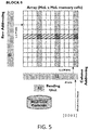
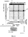
- a winning representation (corresponding to a previous frame in time) is applied by the row addressing unit 42 to the rows of the memory cell array 360, thus enabling a single row. This results to the identification of a certain amount of intersecting cells, as it can be seen in FIG 5 .
- the current frame (represented by the column addressing mask) is temporally correlated to the previous frame (represented by the row addressing). This is done by checking the readout value of all cells in the activated row, and by testing these for a specific criterion, for instance maximum current flowing through one of them, current flowing through cells being larger than a predetermined threshold, minimal resistance of one of the memory cells, resistance of memory cells being below a predetermined threshold, maximal voltage over one of the memory cells, voltage over memory cells being larger than a predetermined threshold, etc. This way, amongst all connections made, the memory cell 40 that fits the criterion most is identified, or the plurality of memory cells that fit the criterion are identified. If, however, a threshold for finding the fit is not reached, no identification is done.
- V G,CC can be selected 25 ⁇ A.
- connection strengths may be weaken the connection strengths that have been developed in the temporal memory arrays. This may for instance be the case when older connections learnt in the past need to be forgotten and replaced by newly learnt patterns, or when certain amount of connections were not due to actual data but to noise and therefore need to be forgotten.
- Weakening of connection strenghts may be done, for instance, by, among the cells of an enabled row, weakening all connections except for the cell that belongs to the winning column.
- This weakening of temporal memories i.e. connections stored in the array
- This weakening of temporal memories i.e. connections stored in the array
- this delearning step can be combined with the reading of the selected row. This means that the condition used to read the selected cells is chosen such that all cells are delearned (connection strengths are weakened).
- the temporal memory system disclosed herein is optionally composed of a Memory Element Load/Store Unit, which is used to implement this operation, as illustrated in FIG. 9 - annotation 92.
- the storing can be facilitated by reading all memory cells of the at least one array and storing them in a dedicated load/store unit.
- the loading (e.g. when excessive training times need to be avoided) is the inverse procedure, whereby the load/store unit loads the desired connection strengths from an outside storage medium (e.g. optical, magnetic, or solid state) to the memory cells of the at least one temporal memory arrays.
- a computer program may be stored/distributed on a suitable medium, such as an optical storage medium or a solid-state medium supplied together with or as part of other hardware, but may also be distributed in other forms, such as via the Internet or other wired or wireless telecommunication systems. Any reference signs in the claims should not be construed as limiting the scope.
Landscapes
- Engineering & Computer Science (AREA)
- Physics & Mathematics (AREA)
- Theoretical Computer Science (AREA)
- Health & Medical Sciences (AREA)
- Life Sciences & Earth Sciences (AREA)
- Biomedical Technology (AREA)
- Biophysics (AREA)
- Mathematical Physics (AREA)
- General Physics & Mathematics (AREA)
- General Engineering & Computer Science (AREA)
- Molecular Biology (AREA)
- Software Systems (AREA)
- Evolutionary Computation (AREA)
- Computing Systems (AREA)
- Data Mining & Analysis (AREA)
- Computational Linguistics (AREA)
- Artificial Intelligence (AREA)
- General Health & Medical Sciences (AREA)
- Neurology (AREA)
- Probability & Statistics with Applications (AREA)
- Semiconductor Memories (AREA)
- Complex Calculations (AREA)
- Memory System (AREA)
- Mram Or Spin Memory Techniques (AREA)
Applications Claiming Priority (1)
| Application Number | Priority Date | Filing Date | Title |
|---|---|---|---|
| EP16180038 | 2016-07-18 |
Publications (3)
| Publication Number | Publication Date |
|---|---|
| EP3273390A2 true EP3273390A2 (de) | 2018-01-24 |
| EP3273390A3 EP3273390A3 (de) | 2018-02-28 |
| EP3273390B1 EP3273390B1 (de) | 2021-12-15 |
Family
ID=56551185
Family Applications (1)
| Application Number | Title | Priority Date | Filing Date |
|---|---|---|---|
| EP17181762.0A Active EP3273390B1 (de) | 2016-07-18 | 2017-07-17 | Hardware-implementierung eines temporären speichersystems |
Country Status (3)
| Country | Link |
|---|---|
| US (1) | US10452972B2 (de) |
| EP (1) | EP3273390B1 (de) |
| KR (1) | KR20180009315A (de) |
Cited By (1)
| Publication number | Priority date | Publication date | Assignee | Title |
|---|---|---|---|---|
| CN109346600A (zh) * | 2018-09-29 | 2019-02-15 | 清华大学 | 一种单器件集成马尔可夫链算法的阻变存储器 |
Families Citing this family (6)
| Publication number | Priority date | Publication date | Assignee | Title |
|---|---|---|---|---|
| US10956814B2 (en) | 2018-08-27 | 2021-03-23 | Silicon Storage Technology, Inc. | Configurable analog neural memory system for deep learning neural network |
| CN109327219B (zh) * | 2018-10-18 | 2022-05-03 | 中国科学院微电子研究所 | 一种基于忆阻器rram的逻辑运算系统 |
| CN109634557B (zh) * | 2018-11-19 | 2021-04-06 | 华中科技大学 | 一种基于1t1r存储器的乘法器及运算方法 |
| KR102368962B1 (ko) * | 2019-03-22 | 2022-03-03 | 국민대학교산학협력단 | 멤리스터 어레이 회로를 제어하기 위한 게이트 회로를 포함하는 뉴럴 네트워크 시스템 |
| US12217166B2 (en) | 2021-05-17 | 2025-02-04 | International Business Machines Corporation | Markov processes using analog crossbar arrays |
| US12016251B2 (en) | 2021-08-25 | 2024-06-18 | International Business Machines Corporation | Spin-orbit torque and spin-transfer torque magnetoresistive random-access memory stack |
Family Cites Families (1)
| Publication number | Priority date | Publication date | Assignee | Title |
|---|---|---|---|---|
| US4803729A (en) * | 1987-04-03 | 1989-02-07 | Dragon Systems, Inc. | Speech recognition method |
-
2017
- 2017-07-13 KR KR1020170089035A patent/KR20180009315A/ko not_active Withdrawn
- 2017-07-14 US US15/650,749 patent/US10452972B2/en active Active
- 2017-07-17 EP EP17181762.0A patent/EP3273390B1/de active Active
Non-Patent Citations (1)
| Title |
|---|
| None |
Cited By (2)
| Publication number | Priority date | Publication date | Assignee | Title |
|---|---|---|---|---|
| CN109346600A (zh) * | 2018-09-29 | 2019-02-15 | 清华大学 | 一种单器件集成马尔可夫链算法的阻变存储器 |
| CN109346600B (zh) * | 2018-09-29 | 2020-04-14 | 清华大学 | 一种单器件集成马尔可夫链算法的阻变存储器 |
Also Published As
| Publication number | Publication date |
|---|---|
| US20180046899A1 (en) | 2018-02-15 |
| US10452972B2 (en) | 2019-10-22 |
| EP3273390B1 (de) | 2021-12-15 |
| EP3273390A3 (de) | 2018-02-28 |
| KR20180009315A (ko) | 2018-01-26 |
Similar Documents
| Publication | Publication Date | Title |
|---|---|---|
| US10452972B2 (en) | Hardware implementation of a temporal memory system | |
| US12242966B2 (en) | Acceleration of model/weight programming in memristor crossbar arrays | |
| CN103917992B (zh) | 用于按概率性方式使用存储器来存储神经网络的突触权重的方法和装置 | |
| US12399655B2 (en) | Parallel memory access and computation in memory devices | |
| US11188825B2 (en) | Mixed-precision deep-learning with multi-memristive devices | |
| JP7316725B2 (ja) | エンコーダ-デコーダ・メモリ拡張ニューラル・ネットワーク・アーキテクチャ | |
| US20120011087A1 (en) | Methods and systems for replaceable synaptic weight storage in neuro-processors | |
| KR20210032140A (ko) | 뉴럴 네트워크에 대한 프루닝을 수행하는 방법 및 장치 | |
| JP6293963B1 (ja) | ニューロモルフィック素子を含むアレイの制御装置、離散化ステップサイズの演算方法およびプログラム | |
| US20200319808A1 (en) | Memory device | |
| US10734448B2 (en) | Convolutional neural network system employing resistance change memory cell array | |
| US11301752B2 (en) | Memory configuration for implementing a neural network | |
| Zhang et al. | The application of non-volatile look-up-table operations based on multilevel-cell of resistance switching random access memory | |
| US20200117449A1 (en) | Accelerated Access to Computations Results Generated from Data Stored in Memory Devices | |
| CN114372496A (zh) | 用于决策树计算的具有模拟内容可寻址存储器(a-cam)的硬件加速器 | |
| JP2019179364A (ja) | 半導体装置、情報処理システム、および情報処理方法 | |
| KR20190131403A (ko) | 3차원 적층 시냅스 구조를 갖는 뉴로모픽 장치 및 이를 포함하는 메모리 장치 | |
| EP3620911A1 (de) | Multiplikations-additions-operationsvorrichtung, multiplikations-additions-operationsverfahren und systeme | |
| CN114997385B (zh) | 应用于神经网络的存内计算架构的操作方法、装置和设备 | |
| EP3685318A1 (de) | Zeitliche bündelung und korrelation in einem künstlichen neuronalen netz | |
| CN115034374B (zh) | 一种图小样本学习的存内计算方法、装置和电子设备 | |
| CN108460453B (zh) | 一种用于ctc训练的数据处理方法、装置及系统 | |
| CN115443469A (zh) | 存储器增强神经网络中的计算机交叉杆阵列 | |
| US20240304254A1 (en) | Memory device for signed multi-bit to multi-bit multiplications | |
| US6198668B1 (en) | Memory cell array for performing a comparison |
Legal Events
| Date | Code | Title | Description |
|---|---|---|---|
| PUAI | Public reference made under article 153(3) epc to a published international application that has entered the european phase |
Free format text: ORIGINAL CODE: 0009012 |
|
| STAA | Information on the status of an ep patent application or granted ep patent |
Free format text: STATUS: THE APPLICATION HAS BEEN PUBLISHED |
|
| AK | Designated contracting states |
Kind code of ref document: A2 Designated state(s): AL AT BE BG CH CY CZ DE DK EE ES FI FR GB GR HR HU IE IS IT LI LT LU LV MC MK MT NL NO PL PT RO RS SE SI SK SM TR |
|
| AX | Request for extension of the european patent |
Extension state: BA ME |
|
| PUAL | Search report despatched |
Free format text: ORIGINAL CODE: 0009013 |
|
| AK | Designated contracting states |
Kind code of ref document: A3 Designated state(s): AL AT BE BG CH CY CZ DE DK EE ES FI FR GB GR HR HU IE IS IT LI LT LU LV MC MK MT NL NO PL PT RO RS SE SI SK SM TR |
|
| AX | Request for extension of the european patent |
Extension state: BA ME |
|
| RIC1 | Information provided on ipc code assigned before grant |
Ipc: G06N 3/04 20060101ALI20180125BHEP Ipc: G06N 3/063 20060101AFI20180125BHEP |
|
| STAA | Information on the status of an ep patent application or granted ep patent |
Free format text: STATUS: REQUEST FOR EXAMINATION WAS MADE |
|
| 17P | Request for examination filed |
Effective date: 20180827 |
|
| RBV | Designated contracting states (corrected) |
Designated state(s): AL AT BE BG CH CY CZ DE DK EE ES FI FR GB GR HR HU IE IS IT LI LT LU LV MC MK MT NL NO PL PT RO RS SE SI SK SM TR |
|
| STAA | Information on the status of an ep patent application or granted ep patent |
Free format text: STATUS: EXAMINATION IS IN PROGRESS |
|
| 17Q | First examination report despatched |
Effective date: 20190328 |
|
| GRAP | Despatch of communication of intention to grant a patent |
Free format text: ORIGINAL CODE: EPIDOSNIGR1 |
|
| STAA | Information on the status of an ep patent application or granted ep patent |
Free format text: STATUS: GRANT OF PATENT IS INTENDED |
|
| INTG | Intention to grant announced |
Effective date: 20210408 |
|
| GRAJ | Information related to disapproval of communication of intention to grant by the applicant or resumption of examination proceedings by the epo deleted |
Free format text: ORIGINAL CODE: EPIDOSDIGR1 |
|
| STAA | Information on the status of an ep patent application or granted ep patent |
Free format text: STATUS: EXAMINATION IS IN PROGRESS |
|
| INTC | Intention to grant announced (deleted) | ||
| GRAP | Despatch of communication of intention to grant a patent |
Free format text: ORIGINAL CODE: EPIDOSNIGR1 |
|
| STAA | Information on the status of an ep patent application or granted ep patent |
Free format text: STATUS: GRANT OF PATENT IS INTENDED |
|
| INTG | Intention to grant announced |
Effective date: 20210913 |
|
| GRAS | Grant fee paid |
Free format text: ORIGINAL CODE: EPIDOSNIGR3 |
|
| GRAA | (expected) grant |
Free format text: ORIGINAL CODE: 0009210 |
|
| STAA | Information on the status of an ep patent application or granted ep patent |
Free format text: STATUS: THE PATENT HAS BEEN GRANTED |
|
| AK | Designated contracting states |
Kind code of ref document: B1 Designated state(s): AL AT BE BG CH CY CZ DE DK EE ES FI FR GB GR HR HU IE IS IT LI LT LU LV MC MK MT NL NO PL PT RO RS SE SI SK SM TR |
|
| REG | Reference to a national code |
Ref country code: GB Ref legal event code: FG4D Ref country code: CH Ref legal event code: EP |
|
| REG | Reference to a national code |
Ref country code: IE Ref legal event code: FG4D Ref country code: DE Ref legal event code: R096 Ref document number: 602017050855 Country of ref document: DE |
|
| REG | Reference to a national code |
Ref country code: AT Ref legal event code: REF Ref document number: 1456034 Country of ref document: AT Kind code of ref document: T Effective date: 20220115 |
|
| REG | Reference to a national code |
Ref country code: LT Ref legal event code: MG9D |
|
| REG | Reference to a national code |
Ref country code: NL Ref legal event code: MP Effective date: 20211215 |
|
| PG25 | Lapsed in a contracting state [announced via postgrant information from national office to epo] |
Ref country code: RS Free format text: LAPSE BECAUSE OF FAILURE TO SUBMIT A TRANSLATION OF THE DESCRIPTION OR TO PAY THE FEE WITHIN THE PRESCRIBED TIME-LIMIT Effective date: 20211215 Ref country code: LT Free format text: LAPSE BECAUSE OF FAILURE TO SUBMIT A TRANSLATION OF THE DESCRIPTION OR TO PAY THE FEE WITHIN THE PRESCRIBED TIME-LIMIT Effective date: 20211215 Ref country code: FI Free format text: LAPSE BECAUSE OF FAILURE TO SUBMIT A TRANSLATION OF THE DESCRIPTION OR TO PAY THE FEE WITHIN THE PRESCRIBED TIME-LIMIT Effective date: 20211215 Ref country code: BG Free format text: LAPSE BECAUSE OF FAILURE TO SUBMIT A TRANSLATION OF THE DESCRIPTION OR TO PAY THE FEE WITHIN THE PRESCRIBED TIME-LIMIT Effective date: 20220315 |
|
| REG | Reference to a national code |
Ref country code: AT Ref legal event code: MK05 Ref document number: 1456034 Country of ref document: AT Kind code of ref document: T Effective date: 20211215 |
|
| PG25 | Lapsed in a contracting state [announced via postgrant information from national office to epo] |
Ref country code: SE Free format text: LAPSE BECAUSE OF FAILURE TO SUBMIT A TRANSLATION OF THE DESCRIPTION OR TO PAY THE FEE WITHIN THE PRESCRIBED TIME-LIMIT Effective date: 20211215 Ref country code: NO Free format text: LAPSE BECAUSE OF FAILURE TO SUBMIT A TRANSLATION OF THE DESCRIPTION OR TO PAY THE FEE WITHIN THE PRESCRIBED TIME-LIMIT Effective date: 20220315 Ref country code: LV Free format text: LAPSE BECAUSE OF FAILURE TO SUBMIT A TRANSLATION OF THE DESCRIPTION OR TO PAY THE FEE WITHIN THE PRESCRIBED TIME-LIMIT Effective date: 20211215 Ref country code: HR Free format text: LAPSE BECAUSE OF FAILURE TO SUBMIT A TRANSLATION OF THE DESCRIPTION OR TO PAY THE FEE WITHIN THE PRESCRIBED TIME-LIMIT Effective date: 20211215 Ref country code: GR Free format text: LAPSE BECAUSE OF FAILURE TO SUBMIT A TRANSLATION OF THE DESCRIPTION OR TO PAY THE FEE WITHIN THE PRESCRIBED TIME-LIMIT Effective date: 20220316 |
|
| PG25 | Lapsed in a contracting state [announced via postgrant information from national office to epo] |
Ref country code: NL Free format text: LAPSE BECAUSE OF FAILURE TO SUBMIT A TRANSLATION OF THE DESCRIPTION OR TO PAY THE FEE WITHIN THE PRESCRIBED TIME-LIMIT Effective date: 20211215 |
|
| PG25 | Lapsed in a contracting state [announced via postgrant information from national office to epo] |
Ref country code: SM Free format text: LAPSE BECAUSE OF FAILURE TO SUBMIT A TRANSLATION OF THE DESCRIPTION OR TO PAY THE FEE WITHIN THE PRESCRIBED TIME-LIMIT Effective date: 20211215 Ref country code: SK Free format text: LAPSE BECAUSE OF FAILURE TO SUBMIT A TRANSLATION OF THE DESCRIPTION OR TO PAY THE FEE WITHIN THE PRESCRIBED TIME-LIMIT Effective date: 20211215 Ref country code: RO Free format text: LAPSE BECAUSE OF FAILURE TO SUBMIT A TRANSLATION OF THE DESCRIPTION OR TO PAY THE FEE WITHIN THE PRESCRIBED TIME-LIMIT Effective date: 20211215 Ref country code: PT Free format text: LAPSE BECAUSE OF FAILURE TO SUBMIT A TRANSLATION OF THE DESCRIPTION OR TO PAY THE FEE WITHIN THE PRESCRIBED TIME-LIMIT Effective date: 20220418 Ref country code: ES Free format text: LAPSE BECAUSE OF FAILURE TO SUBMIT A TRANSLATION OF THE DESCRIPTION OR TO PAY THE FEE WITHIN THE PRESCRIBED TIME-LIMIT Effective date: 20211215 Ref country code: EE Free format text: LAPSE BECAUSE OF FAILURE TO SUBMIT A TRANSLATION OF THE DESCRIPTION OR TO PAY THE FEE WITHIN THE PRESCRIBED TIME-LIMIT Effective date: 20211215 Ref country code: CZ Free format text: LAPSE BECAUSE OF FAILURE TO SUBMIT A TRANSLATION OF THE DESCRIPTION OR TO PAY THE FEE WITHIN THE PRESCRIBED TIME-LIMIT Effective date: 20211215 |
|
| PG25 | Lapsed in a contracting state [announced via postgrant information from national office to epo] |
Ref country code: PL Free format text: LAPSE BECAUSE OF FAILURE TO SUBMIT A TRANSLATION OF THE DESCRIPTION OR TO PAY THE FEE WITHIN THE PRESCRIBED TIME-LIMIT Effective date: 20211215 Ref country code: AT Free format text: LAPSE BECAUSE OF FAILURE TO SUBMIT A TRANSLATION OF THE DESCRIPTION OR TO PAY THE FEE WITHIN THE PRESCRIBED TIME-LIMIT Effective date: 20211215 |
|
| REG | Reference to a national code |
Ref country code: DE Ref legal event code: R097 Ref document number: 602017050855 Country of ref document: DE |
|
| PG25 | Lapsed in a contracting state [announced via postgrant information from national office to epo] |
Ref country code: IS Free format text: LAPSE BECAUSE OF FAILURE TO SUBMIT A TRANSLATION OF THE DESCRIPTION OR TO PAY THE FEE WITHIN THE PRESCRIBED TIME-LIMIT Effective date: 20220415 |
|
| PLBE | No opposition filed within time limit |
Free format text: ORIGINAL CODE: 0009261 |
|
| STAA | Information on the status of an ep patent application or granted ep patent |
Free format text: STATUS: NO OPPOSITION FILED WITHIN TIME LIMIT |
|
| PG25 | Lapsed in a contracting state [announced via postgrant information from national office to epo] |
Ref country code: DK Free format text: LAPSE BECAUSE OF FAILURE TO SUBMIT A TRANSLATION OF THE DESCRIPTION OR TO PAY THE FEE WITHIN THE PRESCRIBED TIME-LIMIT Effective date: 20211215 Ref country code: AL Free format text: LAPSE BECAUSE OF FAILURE TO SUBMIT A TRANSLATION OF THE DESCRIPTION OR TO PAY THE FEE WITHIN THE PRESCRIBED TIME-LIMIT Effective date: 20211215 |
|
| 26N | No opposition filed |
Effective date: 20220916 |
|
| PG25 | Lapsed in a contracting state [announced via postgrant information from national office to epo] |
Ref country code: SI Free format text: LAPSE BECAUSE OF FAILURE TO SUBMIT A TRANSLATION OF THE DESCRIPTION OR TO PAY THE FEE WITHIN THE PRESCRIBED TIME-LIMIT Effective date: 20211215 |
|
| PG25 | Lapsed in a contracting state [announced via postgrant information from national office to epo] |
Ref country code: MC Free format text: LAPSE BECAUSE OF FAILURE TO SUBMIT A TRANSLATION OF THE DESCRIPTION OR TO PAY THE FEE WITHIN THE PRESCRIBED TIME-LIMIT Effective date: 20211215 |
|
| REG | Reference to a national code |
Ref country code: CH Ref legal event code: PL |
|
| GBPC | Gb: european patent ceased through non-payment of renewal fee |
Effective date: 20220717 |
|
| REG | Reference to a national code |
Ref country code: BE Ref legal event code: MM Effective date: 20220731 |
|
| PG25 | Lapsed in a contracting state [announced via postgrant information from national office to epo] |
Ref country code: LU Free format text: LAPSE BECAUSE OF NON-PAYMENT OF DUE FEES Effective date: 20220717 Ref country code: LI Free format text: LAPSE BECAUSE OF NON-PAYMENT OF DUE FEES Effective date: 20220731 Ref country code: FR Free format text: LAPSE BECAUSE OF NON-PAYMENT OF DUE FEES Effective date: 20220731 Ref country code: CH Free format text: LAPSE BECAUSE OF NON-PAYMENT OF DUE FEES Effective date: 20220731 |
|
| PG25 | Lapsed in a contracting state [announced via postgrant information from national office to epo] |
Ref country code: IT Free format text: LAPSE BECAUSE OF FAILURE TO SUBMIT A TRANSLATION OF THE DESCRIPTION OR TO PAY THE FEE WITHIN THE PRESCRIBED TIME-LIMIT Effective date: 20211215 Ref country code: GB Free format text: LAPSE BECAUSE OF NON-PAYMENT OF DUE FEES Effective date: 20220717 Ref country code: BE Free format text: LAPSE BECAUSE OF NON-PAYMENT OF DUE FEES Effective date: 20220731 |
|
| P01 | Opt-out of the competence of the unified patent court (upc) registered |
Effective date: 20230513 |
|
| PG25 | Lapsed in a contracting state [announced via postgrant information from national office to epo] |
Ref country code: IE Free format text: LAPSE BECAUSE OF NON-PAYMENT OF DUE FEES Effective date: 20220717 |
|
| PG25 | Lapsed in a contracting state [announced via postgrant information from national office to epo] |
Ref country code: HU Free format text: LAPSE BECAUSE OF FAILURE TO SUBMIT A TRANSLATION OF THE DESCRIPTION OR TO PAY THE FEE WITHIN THE PRESCRIBED TIME-LIMIT; INVALID AB INITIO Effective date: 20170717 |
|
| PG25 | Lapsed in a contracting state [announced via postgrant information from national office to epo] |
Ref country code: MK Free format text: LAPSE BECAUSE OF FAILURE TO SUBMIT A TRANSLATION OF THE DESCRIPTION OR TO PAY THE FEE WITHIN THE PRESCRIBED TIME-LIMIT Effective date: 20211215 Ref country code: CY Free format text: LAPSE BECAUSE OF FAILURE TO SUBMIT A TRANSLATION OF THE DESCRIPTION OR TO PAY THE FEE WITHIN THE PRESCRIBED TIME-LIMIT Effective date: 20211215 |
|
| PG25 | Lapsed in a contracting state [announced via postgrant information from national office to epo] |
Ref country code: TR Free format text: LAPSE BECAUSE OF FAILURE TO SUBMIT A TRANSLATION OF THE DESCRIPTION OR TO PAY THE FEE WITHIN THE PRESCRIBED TIME-LIMIT Effective date: 20211215 |
|
| PG25 | Lapsed in a contracting state [announced via postgrant information from national office to epo] |
Ref country code: MT Free format text: LAPSE BECAUSE OF FAILURE TO SUBMIT A TRANSLATION OF THE DESCRIPTION OR TO PAY THE FEE WITHIN THE PRESCRIBED TIME-LIMIT Effective date: 20211215 |
|
| PGFP | Annual fee paid to national office [announced via postgrant information from national office to epo] |
Ref country code: DE Payment date: 20250620 Year of fee payment: 9 |