EP3272005B1 - Oscillateur commandé en tension à inductance à prises - Google Patents
Oscillateur commandé en tension à inductance à prises Download PDFInfo
- Publication number
- EP3272005B1 EP3272005B1 EP16764246.1A EP16764246A EP3272005B1 EP 3272005 B1 EP3272005 B1 EP 3272005B1 EP 16764246 A EP16764246 A EP 16764246A EP 3272005 B1 EP3272005 B1 EP 3272005B1
- Authority
- EP
- European Patent Office
- Prior art keywords
- amplifier
- voltage
- inductor
- impedance
- circuit
- Prior art date
- Legal status (The legal status is an assumption and is not a legal conclusion. Google has not performed a legal analysis and makes no representation as to the accuracy of the status listed.)
- Active
Links
Images




Classifications
-
- H—ELECTRICITY
- H03—ELECTRONIC CIRCUITRY
- H03B—GENERATION OF OSCILLATIONS, DIRECTLY OR BY FREQUENCY-CHANGING, BY CIRCUITS EMPLOYING ACTIVE ELEMENTS WHICH OPERATE IN A NON-SWITCHING MANNER; GENERATION OF NOISE BY SUCH CIRCUITS
- H03B5/00—Generation of oscillations using amplifier with regenerative feedback from output to input
- H03B5/08—Generation of oscillations using amplifier with regenerative feedback from output to input with frequency-determining element comprising lumped inductance and capacitance
- H03B5/12—Generation of oscillations using amplifier with regenerative feedback from output to input with frequency-determining element comprising lumped inductance and capacitance active element in amplifier being semiconductor device
- H03B5/1228—Generation of oscillations using amplifier with regenerative feedback from output to input with frequency-determining element comprising lumped inductance and capacitance active element in amplifier being semiconductor device the amplifier comprising one or more field effect transistors
-
- G—PHYSICS
- G06—COMPUTING OR CALCULATING; COUNTING
- G06F—ELECTRIC DIGITAL DATA PROCESSING
- G06F30/00—Computer-aided design [CAD]
- G06F30/30—Circuit design
- G06F30/36—Circuit design at the analogue level
-
- G—PHYSICS
- G06—COMPUTING OR CALCULATING; COUNTING
- G06F—ELECTRIC DIGITAL DATA PROCESSING
- G06F30/00—Computer-aided design [CAD]
- G06F30/30—Circuit design
- G06F30/39—Circuit design at the physical level
-
- H—ELECTRICITY
- H03—ELECTRONIC CIRCUITRY
- H03B—GENERATION OF OSCILLATIONS, DIRECTLY OR BY FREQUENCY-CHANGING, BY CIRCUITS EMPLOYING ACTIVE ELEMENTS WHICH OPERATE IN A NON-SWITCHING MANNER; GENERATION OF NOISE BY SUCH CIRCUITS
- H03B5/00—Generation of oscillations using amplifier with regenerative feedback from output to input
- H03B5/08—Generation of oscillations using amplifier with regenerative feedback from output to input with frequency-determining element comprising lumped inductance and capacitance
- H03B5/12—Generation of oscillations using amplifier with regenerative feedback from output to input with frequency-determining element comprising lumped inductance and capacitance active element in amplifier being semiconductor device
- H03B5/1206—Generation of oscillations using amplifier with regenerative feedback from output to input with frequency-determining element comprising lumped inductance and capacitance active element in amplifier being semiconductor device using multiple transistors for amplification
-
- H—ELECTRICITY
- H03—ELECTRONIC CIRCUITRY
- H03B—GENERATION OF OSCILLATIONS, DIRECTLY OR BY FREQUENCY-CHANGING, BY CIRCUITS EMPLOYING ACTIVE ELEMENTS WHICH OPERATE IN A NON-SWITCHING MANNER; GENERATION OF NOISE BY SUCH CIRCUITS
- H03B5/00—Generation of oscillations using amplifier with regenerative feedback from output to input
- H03B5/08—Generation of oscillations using amplifier with regenerative feedback from output to input with frequency-determining element comprising lumped inductance and capacitance
- H03B5/12—Generation of oscillations using amplifier with regenerative feedback from output to input with frequency-determining element comprising lumped inductance and capacitance active element in amplifier being semiconductor device
- H03B5/1206—Generation of oscillations using amplifier with regenerative feedback from output to input with frequency-determining element comprising lumped inductance and capacitance active element in amplifier being semiconductor device using multiple transistors for amplification
- H03B5/1212—Generation of oscillations using amplifier with regenerative feedback from output to input with frequency-determining element comprising lumped inductance and capacitance active element in amplifier being semiconductor device using multiple transistors for amplification the amplifier comprising a pair of transistors, wherein an output terminal of each being connected to an input terminal of the other, e.g. a cross coupled pair
-
- H—ELECTRICITY
- H03—ELECTRONIC CIRCUITRY
- H03B—GENERATION OF OSCILLATIONS, DIRECTLY OR BY FREQUENCY-CHANGING, BY CIRCUITS EMPLOYING ACTIVE ELEMENTS WHICH OPERATE IN A NON-SWITCHING MANNER; GENERATION OF NOISE BY SUCH CIRCUITS
- H03B5/00—Generation of oscillations using amplifier with regenerative feedback from output to input
- H03B5/08—Generation of oscillations using amplifier with regenerative feedback from output to input with frequency-determining element comprising lumped inductance and capacitance
- H03B5/12—Generation of oscillations using amplifier with regenerative feedback from output to input with frequency-determining element comprising lumped inductance and capacitance active element in amplifier being semiconductor device
- H03B5/1237—Generation of oscillations using amplifier with regenerative feedback from output to input with frequency-determining element comprising lumped inductance and capacitance active element in amplifier being semiconductor device comprising means for varying the frequency of the generator
- H03B5/124—Generation of oscillations using amplifier with regenerative feedback from output to input with frequency-determining element comprising lumped inductance and capacitance active element in amplifier being semiconductor device comprising means for varying the frequency of the generator the means comprising a voltage dependent capacitance
- H03B5/1243—Generation of oscillations using amplifier with regenerative feedback from output to input with frequency-determining element comprising lumped inductance and capacitance active element in amplifier being semiconductor device comprising means for varying the frequency of the generator the means comprising a voltage dependent capacitance the means comprising voltage variable capacitance diodes
-
- H—ELECTRICITY
- H03—ELECTRONIC CIRCUITRY
- H03B—GENERATION OF OSCILLATIONS, DIRECTLY OR BY FREQUENCY-CHANGING, BY CIRCUITS EMPLOYING ACTIVE ELEMENTS WHICH OPERATE IN A NON-SWITCHING MANNER; GENERATION OF NOISE BY SUCH CIRCUITS
- H03B5/00—Generation of oscillations using amplifier with regenerative feedback from output to input
- H03B5/08—Generation of oscillations using amplifier with regenerative feedback from output to input with frequency-determining element comprising lumped inductance and capacitance
- H03B5/12—Generation of oscillations using amplifier with regenerative feedback from output to input with frequency-determining element comprising lumped inductance and capacitance active element in amplifier being semiconductor device
- H03B5/1237—Generation of oscillations using amplifier with regenerative feedback from output to input with frequency-determining element comprising lumped inductance and capacitance active element in amplifier being semiconductor device comprising means for varying the frequency of the generator
- H03B5/1256—Generation of oscillations using amplifier with regenerative feedback from output to input with frequency-determining element comprising lumped inductance and capacitance active element in amplifier being semiconductor device comprising means for varying the frequency of the generator the means comprising a variable inductance
- H03B5/1259—Generation of oscillations using amplifier with regenerative feedback from output to input with frequency-determining element comprising lumped inductance and capacitance active element in amplifier being semiconductor device comprising means for varying the frequency of the generator the means comprising a variable inductance the means comprising a variable active inductor, e.g. gyrator circuits
-
- H—ELECTRICITY
- H03—ELECTRONIC CIRCUITRY
- H03B—GENERATION OF OSCILLATIONS, DIRECTLY OR BY FREQUENCY-CHANGING, BY CIRCUITS EMPLOYING ACTIVE ELEMENTS WHICH OPERATE IN A NON-SWITCHING MANNER; GENERATION OF NOISE BY SUCH CIRCUITS
- H03B5/00—Generation of oscillations using amplifier with regenerative feedback from output to input
- H03B5/08—Generation of oscillations using amplifier with regenerative feedback from output to input with frequency-determining element comprising lumped inductance and capacitance
- H03B5/12—Generation of oscillations using amplifier with regenerative feedback from output to input with frequency-determining element comprising lumped inductance and capacitance active element in amplifier being semiconductor device
- H03B5/1296—Generation of oscillations using amplifier with regenerative feedback from output to input with frequency-determining element comprising lumped inductance and capacitance active element in amplifier being semiconductor device the feedback circuit comprising a transformer
-
- G—PHYSICS
- G06—COMPUTING OR CALCULATING; COUNTING
- G06F—ELECTRIC DIGITAL DATA PROCESSING
- G06F2115/00—Details relating to the type of the circuit
- G06F2115/06—Structured ASICs
-
- H—ELECTRICITY
- H03—ELECTRONIC CIRCUITRY
- H03B—GENERATION OF OSCILLATIONS, DIRECTLY OR BY FREQUENCY-CHANGING, BY CIRCUITS EMPLOYING ACTIVE ELEMENTS WHICH OPERATE IN A NON-SWITCHING MANNER; GENERATION OF NOISE BY SUCH CIRCUITS
- H03B2200/00—Indexing scheme relating to details of oscillators covered by H03B
- H03B2200/0002—Types of oscillators
- H03B2200/0012—Pierce oscillator
-
- H—ELECTRICITY
- H03—ELECTRONIC CIRCUITRY
- H03B—GENERATION OF OSCILLATIONS, DIRECTLY OR BY FREQUENCY-CHANGING, BY CIRCUITS EMPLOYING ACTIVE ELEMENTS WHICH OPERATE IN A NON-SWITCHING MANNER; GENERATION OF NOISE BY SUCH CIRCUITS
- H03B2200/00—Indexing scheme relating to details of oscillators covered by H03B
- H03B2200/003—Circuit elements of oscillators
- H03B2200/004—Circuit elements of oscillators including a variable capacitance, e.g. a varicap, a varactor or a variable capacitance of a diode or transistor
Definitions
- This disclosure is generally directed to voltage controlled oscillators (VCOs) and more particularly to a VCO employing an integrated tapped inductor with a novel topology and layout to improve noise performance and reduce power consumption.
- VCOs voltage controlled oscillators
- VCOs voltage controlled oscillators
- a VCO may be embodied as a stand-alone module separate from other circuits or integrated into an application specific integrated circuit (ASIC), for use in devices such as, but not limited to, handsets, base stations, and virtually every communication device.
- ASIC application specific integrated circuit
- the noise performance of a LC resonant VCO is directly related to its signal power, which is proportional to the energy stored in the resonant inductor-capacitor (LC) tank circuit.
- the energy stored in the LC circuit is proportional to the size of the inductor and the square of the supply voltage for the amplifier in the VCO.
- HCI hot carrier injection
- the inductor used in the LC tank circuit must also decrease in size so that the resulting noise performance of the VCO remains the same. Increases in required frequency also require the inductor size to be decreased. The decrease in inductor size presents a challenge since as an inductor gets smaller in size, its quality factor (Q) decreases as well, further increasing the thermal noise of the VCO.
- a so-called Hartley VCO is an active circuit comprising an amplifier, capacitor(s), and inductors.
- a characteristic of the Hartley VCO is a tuned circuit comprising capacitor(s) in parallel with two or more inductors in series, and a feedback signal for oscillation taken from a connection in between the inductors.
- Transistors M1-M4 form an amplifier.
- PMOS transistors M3 and M4 have their sources coupled to the positive supply rail (e.g. VDD), and their respective gates cross coupled to the drains of the opposing PMOS transistor and to the sources of PMOS transistors M1 and M2, respectively.
- PMOS transistors M1 and M2 have their drains coupled to the negative supply rail (e.g. ground), and their respective gates coupled to the conventional LC tank resonator formed with inductors L1 and L2 and capacitors C v .
- FIGURE 2 illustrates a prior art layout for tapped inductors L1 and L2 schematically depicted in FIGURE 1 .
- the inductors L1 and L2 are shown as nested loops 201-202. The nesting provides the mutual couplings k1 and k2 shown in FIGURE 1 .
- U.S. Patent 7,583,156 shows nested loops in FIGs. 2a, 2b and 2d.
- U.S. Patent 7,583,156 shows parallel coupled loops in FIG. 2 .
- FIGURE 3A illustrates a schematic diagram of a prior art simplified differential Harley VCO circuit employing a conventional LC tank circuit resonator.
- FIGURE 3B illustrates a simplified schematic diagram of the small signal half circuit resonator of the circuit in FIGURE 3A .
- FIGURE 4 illustrates an integrated circuit die for the circuit depicted in FIGURES 3A and 3B including the prior art layout for the tapped inductors.
- the inductor elements L1 and L2 are shown as nested loops 401-402. The nesting provides the mutual coupling K shown in FIGURE 3A .
- Inductive elements L3 and L4 in FIGURE 3A are shown as separate loops 403-404 in FIGURE 4 .
- the invention is defined by apparatus claim 1.
- a non-transitory computer-readable medium for use with a computer having software for creating integrated circuits according to claim 6.
- the present disclosure provides a VCO with reduced current, lower noise, higher Q at higher frequencies, and better linearity.
- circuits or other components may be described or claimed as “configured to” perform a task or tasks.
- “configured to” is used to connote structure by indicating that the circuits/components include structure (e.g., circuitry) that performs the task or tasks during operation. As such, the circuit/component can be said to be configured to perform the task even when the specified circuit/component is not currently operational (e.g., is not on).
- the circuits/components used with the "configured to” language include hardware - for example, circuits to implement the operation, etc. Reciting that a circuit/component is “configured to” perform one or more tasks is expressly intended not to invoke 35 U.S.C. 112 (f).
- FIGURE 5 a schematic of an LC resonant circuit 500 including parasitic resistances R c and R l is illustrated for use in a differential VCO.
- the VCO amplifier supplies a current to the input impedance of the LC circuit 500 that produces a voltage across the LC circuit equal to the voltage at the input of the amplifier.
- the amplifier drives the impedance Z 2 ( ⁇ o ) and the voltage at the input of the amplifier is that indicated as being across Z 2 ( ⁇ o ).
- a single inductor is tapped (e.g., divided into at least two parts) in a manner described by a coefficient K.
- the amplifier drives the inductor tap defined by impedance Z 1 ( ⁇ o ) while the voltage at the input of the amplifier is from a signal across the inductor tap defined by impedance Z 2 ( ⁇ o ).
- inductor segments KL and (1-K)/2*L can be viewed as separate inductors for small inductances and very high frequencies. However, separate inductors are impractical due to the physical size requirements and mutual coupling.
- the input and the output of the amplifier are at different points in the LC circuit (i.e. Z 2 and Z 1 ), the input voltage to the amplifier in the VCO can be much larger than its output voltage as determined by the voltage divider action of the tapped inductor. There are a number of advantages to this arrangement.
- the HCI voltage limitations of the amplifier are constrained to the output. This allows the input signal to exceed the supply voltage restrictions of the amplifier. Since the input voltage is representative of the energy stored in the LC circuit, the VCO noise is lower for the same total inductance than a VCO with a traditional resonator because the LC circuit voltage is higher. Moreover, the inductor does not have to decrease in size to meet noise requirements allowing for a higher inductor Q when integrated onto an integrated circuit, such as, for example, as part of an ASIC.
- the output current of the amplifier is the product of the input voltage across Z 2 and its transconductance g m . Since the input voltage is increased, the amplifier has more gain for the same current. This reduces the power requirements for the system.
- the impedance of the LC circuit at Z 1 ( ⁇ o ) is lower than the impedance Z 2 ( ⁇ o ) by a factor of K 2 .
- the linearity of the amplifier under large signal conditions is dominated by the linearity at its output rather than its input.
- Having a lower impedance at the output of the VCO reduces the non-linear mixing of flicker noise to the VCO frequency thus improving its close-in sideband noise spectrum.
- flicker noise at baseband frequencies is a type of electronic noise with a 1/ ⁇ density spectrum but once mixed by nonlinear elements, produces a 1/ ⁇ 3 portion of the VCO single side band phase noise.
- ⁇ o is the oscillation frequency (rad/s)
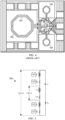
- FIGURE 6 illustrates an example layout for a differential tapped inductor 600 for use in an LC tank circuit (such as that shown in FIGURE 5 ) and for integration onto an integrated circuit in accordance with principles of the present invention.
- FIGURE 7 illustrates an ideal schematic of a differential LC tank circuit resonator 702 including representation of the equivalent inductances 600' of the tapped inductor 600 in FIGURE 6 coupled in parallel with a capacitor C. Note that the segments V1-V5a, V2-V5a, V3-V5b, V4-V5b, and V5a-V5b in FIGURE 6 correspond to inductors L1, L2, L3, L4, and L5 in the schematic of FIGURE 7 , respectively.
- the differential tapped inductor 600 comprises one or more conductive segments (e.g. V1-V5a, V4-V5b, and V5a-V5b) forming a physical loop 601.
- the term "physical loop” refers to a closed or nearly closed geometric shape having beginning and ending points that are co-located or in close proximity to each other, and that includes at least one substantially convex portion that defines an interior space within the convex portion (e.g., a cyclic polygon or cyclic polygon segment).
- a physical loop is to be distinguished from an "electrical loop" which typically represents a closed path of any shape through which electrical current may flow.
- the physical loop 601 is preferably symmetrical and, in the case of the inductor 600, is depicted as a generally octagonal shape. Those skilled in the art will recognize that the physical loop 601 may include other symmetrical and non-symmetrical shapes without departing from the scope of the present disclosure (e.g., a rectangle, square, hexagon, etc.).
- the inductor 600 is tapped with electrical connections at V5a and V5b with segments V2-V5a and V3-V5b forming electrical loops (L2 and L3) disposed within the interior space formed by the physical loop 601 (including L1, L5, and L4).
- the capacitive element C of resonator 702 may be embodied as a PMOS varactor, an NMOS varactor, a metal-insulator-metal (MIM) device, or any other suitable capacitance element.
- MIM metal-insulator-metal
- two types of varactors may be employed namely, a reversed-bias pn junction diode or a MOS capacitor varactor.
- the MOS capacitor varactor may be formed with a MOS transistor having its drain, source, and bulk connections coupled together and adjusting the capacitance based on the voltage applied between the bulk and the gate connections.
- the quality factor (Q) for the resonant LC tank circuit 702 is dependent on the inductor 600 having low resistance.
- the resistance of the inductor 600 is minimized by using a thick/wide metallization process such as, but not limited to, aluminum, copper, gold, or other appropriate material to reduce the series resistance.
- the inductor 600 is preferably formed over a high dielectric substrate material such as silicon, gallium arsenide, or other appropriate material. Surface micro-machining technologies may be employed to create an air gap between the inductor and the substrate to further increase the dielectric property.
- L2 and L3 segments may be constructed with a thinner metal material as depicted in FIGURE 6 .
- a practical problem associated with using multiple inductors is the mutual inductance in any connection from the amplifier output to the tap points V5a and V5b.
- the inductor current in the resonant LC circuit is typically much higher than the current supplied from the amplifier by a factor of the circuit Q.
- the mutual inductance is high, the induced current from the resonant LC circuit becomes high enough in the leads from the amplifier output to the tap point that the input impedance to the tap becomes so high that the amplifier cannot supply any current.
- tap segments V2-V5a (L2) and V3-V5b (L3) are routed up the middle of the inductor 600 (as depicted in FIGURE 6 ) so that the induced currents from the symmetric halves of the inductor 600 cancel.
- Tap locations V5a and V5b can be adjusted in metal to vary the power consumption, VCO output swing, and phase noise performance. This can be used to fine tune a design held at metal such as depicted by V5a' and V5b'.
- the substrate may be doped to have a high resistivity and/or the distance between the metal layer and the substrate may be increased through etching or micro-machining.
- FIGURE 8 illustrates a block diagram of a differential VCO 800 practiced in accordance with principles of the present disclosure.
- the tapped LC tank circuit 702 (illustrated in detail in FIGURE 7 ) has terminals V1, V2, V3, and V4. Terminals V1 and V4 are coupled to the input of amplifier 804 and terminals V2 and V3 are coupled to the output of amplifier 804.
- Amplifier 804 preferably has a CMOS topology however those skilled in the art will recognize other suitable amplifier topologies such as PMOS, NMOS and bipolar, without departing from the scope of the present disclosure.
- a CMOS amplifier is formed with PMOS transistors 904 and 906 and NMOS transistors 908 and 910.
- the PMOS transistors 904 and 906 have their sources coupled to the positive supply rail (VDD) and their gates coupled to the gates of NMOS transistors 908 and 910, respectively.
- the gates of PMOS transistor 904 and NMOS transistor 908 are coupled to the V1 tap of differential tapped LC tank circuit 702.
- the gates of PMOS transistor 906 and NMOS transistor 910 are coupled to the V4 tap of differential tapped LC tank circuit 702.
- the NMOS transistors 908 and 910 have their sources coupled to the negative supply rail (ground) and their respective drains coupled to the drains of PMOS transistors 904 and 906, respectively.
- V3 and V4 taps of the LC tank resonator circuit 702 are coupled to the commonly coupled drains of PMOS transistor 904 and NMOS transistor 908 and commonly coupled drains of PMOS transistor 906 and NMOS transistor 910, respectively.
- the single ended tapped inductor 1000 comprises one or more conductive segments (e.g. V1-1002 and 1002-V3) forming a physical loop 1001.
- the physical loop 1001 is preferably symmetrical and is depicted in a generally octagonal shape. Those skilled in the art will recognize other symmetrical and non-symmetrical shapes for the physical loop 1001 without departing from the scope of the present disclosure.
- the inductor 1000 is tapped with at least one electrical connection (e.g., 1002) with a segment 1002-V2 disposed within the interior of the physical loop 1001.
- FIGURE 11 illustrates a schematic of an ideal single ended LC tank circuit resonator 1102 including a representation of the equivalent inductances of the tapped inductor 1000 in FIGURE 10 coupled in parallel with a capacitor C.
- the capacitive element C of resonator 1102 may be embodied as a PMOS varactor, an NMOS varactor, a metal-insulator-metal (MIM) device, or any other suitable capacitance element.
- MIM metal-insulator-metal
- two types of varactors may be employed namely, a reversed-bias pn junction diode or a MOS capacitor varactor.
- the MOS capacitor varactor may be formed with a MOS transistor having its drain, source, and bulk connections coupled together and adjusting the capacitance based on the voltage applied between the bulk and the gate connections.
- the quality factor (Q) for the resonant LC tank circuit 1102 is dependent on the inductor 1000 having low resistance.
- the resistance of the inductor is minimized by using a thick/wide metallization process such as, but not limited to, aluminum, copper, or other appropriate material to reduce the series resistance.
- the inductor 1000 is preferably formed over a high dielectric substrate material such as silicon, gallium arsenide, or other appropriate material. Surface micro-machining technologies may be employed to create an air gap between the inductor and the substrate to further increase the dielectric property.
- the inductor tap segment L2 which is coupled to the amplifier output is not part of the LC resonant circuit. Accordingly, its parasitic resistance is not as critical as the parasitic resistances of inductor segments of L1 and L3. Thus, the L2 segment may be constructed with a thinner metal material as depicted in FIGURE 10 .
- FIGURE 12 a schematic is illustrated of a single ended LC resonant circuit 1200 including parasitic resistances R c and R l for use in a single ended VCO.
- a single ended VCO amplifier supplies a current to the input impedance of the LC circuit 1200 which produces a voltage across the LC circuit equal to the voltage at the input of the amplifier.
- the amplifier drives the impedance Z 2 ( ⁇ o ) and the voltage at the input of the amplifier is that indicated as being across Z 2 ( ⁇ o ).
- the inductor is tapped (e.g. divided into at least two parts) described by a coefficient K.
- the amplifier drives the inductor tap defined by impedance Z 1 ( ⁇ o ) while the voltage at the input of the amplifier is from a signal across the inductor tap defined by impedance Z 2 ( ⁇ o ).
- inductor segments KL and (1-K)L can be viewed as separate inductors for small inductances and very high frequencies. However, separate inductors are impractical due to the physical size requirements and mutual coupling.
- the input voltage to the amplifier in the VCO can be much larger than its output voltage as determined by the voltage divider action of the tapped inductor.
- FIGURE 13 a schematic is illustrated of an example single ended VCO 1300 employing an amplifier having a CMOS topology and a resonator 1102 practiced in accordance with the principles of the present disclosure.
- a CMOS amplifier is formed with PMOS transistor 1302 and NMOS transistor 1304.
- PMOS transistor 1302 has its source coupled to the positive supply rail (VDD) and its gate coupled to the gate of NMOS transistor 1304 and to the V1 tap of single ended tapped LC tank circuit 1102.
- the NMOS transistor 1304 has its source coupled to the negative supply rail (ground) and its drain coupled to the drain of PMOS transistor 1304 and to the V2 tap of single ended tapped LC tank circuit 1102.
- the V3 tap of the single ended tapped LC tank circuit 1102 is coupled to the negative supply rail (ground).
- circuit in FIGURE 13 preferably has a CMOS topology
- those skilled in the art will recognize other suitable amplifier topologies such as PMOS, NMOS and bipolar, without departing from the scope of the present disclosure.
- EDA Electronic Design Automation
- FIGURE 14 illustrating a simplified general ASIC design flow employing (EDA) tools for producing ASICs having embodiments of the present disclosure.
- EDA electronic circuit design
- the functional design is typically manifested by writing Register Transfer Level (RTL) code in a Hardware Descriptive Language (HDL) such as but not limited to, VHDL or Verilog.
- RTL Register Transfer Level
- HDL Hardware Descriptive Language
- a functional verification is then preferably performed on the HDL data structures to ensure the RTL design is in accordance with the logic specifications.
- a schematic of the digital logic can be captured with a schematic capture program.
- the analog functional design is typically manifested by capturing a schematic with a schematic capture program.
- the output of the schematic capture program is then converted (synthesized) into gate/transistor level netlist data structures.
- the data structures are simulated with a simulation program with integrated circuits emphasis (SPICE).
- SPICE simulation program with integrated circuits emphasis
- the data structures from step 1402 are instantiated with their geometric representations and the physical layout of the ASIC is performed.
- the first step in physical layout is typically so-called "floor-planning" wherein gross regions on the integrated circuit chip are assigned and input/output (I/O) pins are defined.
- Hard cores e.g. arrays, analog blocks, inductors, etc.
- Clock wiring commonly referred to as clock trees
- Postwiring optimization is preferably performed to improve performance (timing closure), noise (signal integrity), and yield.
- the layout is modified, where possible, while maintaining compliance with the design rules set by the captive or external semiconductor manufacturing foundry of choice, to make it more efficient to produce. Such modifications may include adding extra vias or dummy metal/diffusion/poly layers.
- the physical designed is verified.
- Design rule checking is performed to determine whether the physical layout of the ASIC satisfies a series of recommended parameters i.e. design rules of the foundry.
- the design rules are a series of parameters provided by the foundry that are specific to a particular semiconductor manufacturing process.
- the design rules specify certain geometric and connectivity restrictions to ensure sufficient margins to account for variability in semiconductor manufacturing processes, to ensure that the ASICs work correctly.
- a layout versus schematic (LVS) check is preferably performed to verify the physical layout corresponds to the original schematic or circuit diagram of the design.
- a complete simulation is then preferably performed to ensure the layout phase is properly done.
- mask generation design data typically in the form of GDSII data structures is said to "tapeout" for preparation of photomasks at step 1408.
- the GDSII data structures are transferred through a communications medium (e.g. storage or over a network) from the circuit designer to either a photomask supplier/maker or directly to the semiconductor foundry.
- the photomasks are created and used to manufacture ASICs in accordance with principles of the present disclosure.
- Some of the techniques described herein can be implemented by software stored on one or more computer readable storage medium and executed on a computer.
- the selected techniques could be executed on a single computer or a computer networked with another computer or computers.
- Product details well known in the art may be omitted.
- FIGURE 15 shows an illustrative example of a computing device 1501 for practicing the design flow of FIGURE 15 .
- the computing device 1501 includes a computing unit 1503 with a processing unit 1505 and a system memory 1507.
- the processing unit 1505 may be any type of programmable electronic device for executing software instructions, but will conventionally be a microprocessor.
- the system memory 1507 may include both a read-only memory (ROM) 1509 and a random access memory (RAM) 1511. As will be appreciated by those of ordinary skill in the art, both the read-only memory 1509 and the random access memory 1511 may store software instructions for execution by the processing unit 1505.
- the processing unit 1505 and the system memory 1507 are connected, either directly or indirectly, through a bus 1513 or alternate communication structure, to one or more peripheral devices.
- the processing unit 1505 or the system memory 1507 may be directly or indirectly connected to one or more additional memory storage devices 1515.
- the memory storage devices 1515 may include, for example, a "hard" magnetic disk drive, a solid state disk drive, an optical disk drive, and a removable disk drive.
- the processing unit 1505 and the system memory 1507 also may be directly or indirectly connected to one or more input devices 1517 and one or more output devices 1519.
- the input devices 1517 may include, for example, a keyboard, a pointing device (such as a mouse, touchpad, stylus, trackball, or joystick), a scanner, a camera, and a microphone.
- the output devices 1519 may include, for example, a display device, a printer and speakers.
- one or more of the peripheral devices 1515-1519 may be internally housed with the computing unit 1503. Alternately, one or more of the peripheral devices 1515-1519 may be external to the housing for the computing unit 1503 and connected to the bus 1513 through, for example, a Universal Serial Bus (USB) connection or a digital visual interface (DVI) connection.
- USB Universal Serial Bus
- DVI digital visual interface
- the computing unit 1503 may also be directly or indirectly connected to one or more network interfaces cards (NIC) 1521, for communicating with other devices making up a network.
- the network interface cards 1521 translate data and control signals from the computing unit 1503 into network messages according to one or more communication protocols, such as the transmission control protocol (TCP) and the Internet protocol (IP).
- TCP transmission control protocol
- IP Internet protocol
- the network interface cards 1521 may employ any suitable connection agent (or combination of agents) for connecting to a network, including, for example, a wireless transceiver, a modem, or an Ethernet connection.
- computing device 1501 is illustrated as an example only, and it not intended to be limiting. Various embodiments of the invention may be implemented using one or more computing devices that include the components of the computing device 1501 illustrated in FIGURE 15 , or which include an alternate combination of components, including components that are not shown in FIGURE 15 . For example, various embodiments of the invention may be implemented using a multi-processor computer, a plurality of single and/or multiprocessor computers arranged into a network, or some combination of both.
- a resonator means having inductive and capacitive means includes at least two conductive segments that form a conductive loop and an amplification means coupled to at least one conductive segment of the resonator means forming impedance means.
- the impedance means includes first and second impedance means.
- the at least two conductive segments form two electrical loops symmetrically disposed within the interior space formed by the resonator means.
- a computer means in another embodiment, includes storage means for storing computer instructions having photomask data means for making an oscillator comprising resonator means.
- the resonator means having inductive and capacitive means that includes at least two conductive segments that form a conductive loop.
- the resonator means includes an amplification means coupled to at least one conductive segment of the resonator means forming impedance means.
- the impedance means includes first and second impedance means.
- the at least two conductive segments form two electrical loops symmetrically disposed within the interior space formed by the resonator means.
- a floor planning means includes logic for defining or assigning gross regions on the integrated circuit and for defining input/output (I/O) pins.
- the floor planning means includes hard core (e.g. arrays, analog blocks, inductors, etc) placing means for placing within the gross regions based on the design constraints (e.g. trace lengths, timing etc.).
- Clock wiring placing means (commonly referred to as clock trees) are configured for placing clock trees and for routing connections between gates/analog blocks.
- a global and detailed routing means is configured to design connections to connect all the elements together.
- Physical design verification means that includes design rule checking means is used to verify the physical design of the circuit (e.g., an ASIC) satisfies one or more design rules.
- the design rules specify certain geometric and connectivity restrictions to ensure sufficient margins to account for variability in semiconductor manufacturing processes, to ensure that the ASICs work correctly.
- a layout versus schematic (LVS) means is configured to verify the physical layout corresponds to the original schematic or circuit diagram of the design.
- a simulation means is configured to perform a complete simulation to ensure the layout phase is properly done.
- Tapeout means is configured to generate mask generation design data typically in the form of GDSII data structures for preparation of photomasks.
- the GDSII data structures are transferred through a communications medium (e.g. storage or over a network) from the circuit designer to either a photomask supplier/maker or directly to the semiconductor foundry.
- Photomask creation means create photomasks that are used to manufacture ASICs in accordance with principles of the present disclosure.
- the above described means are configured as appropriate to generate resonator and amplification means as described and claimed herein.
- Some of the techniques described herein can be implemented by software stored on one or more computer readable storage medium and executed on a computer.
- the selected techniques could be executed on a single computer or a computer networked with another computer or computers.
- Product details well known in the art may be omitted.
- ROM read only memory
- RAM random access memory
- register cache memory
- semiconductor memory devices magnetic media such as internal hard disks and removable disks, magneto-optical media, and optical media such as CD-ROM disks, and digital versatile disks (DVDs).
Landscapes
- Engineering & Computer Science (AREA)
- Power Engineering (AREA)
- Computer Hardware Design (AREA)
- Physics & Mathematics (AREA)
- Theoretical Computer Science (AREA)
- Evolutionary Computation (AREA)
- Geometry (AREA)
- General Engineering & Computer Science (AREA)
- General Physics & Mathematics (AREA)
- Inductance-Capacitance Distribution Constants And Capacitance-Resistance Oscillators (AREA)
- Semiconductor Integrated Circuits (AREA)
Claims (10)
- Oscillateur commandé en tension comprenant :un résonateur (500) comportant un élément capacitif et un élément inductif, l'élément inductif comportant une pluralité de segments conducteurs (L1, L4, L5) formant une boucle physique unique présentant une première borne (V1) et une quatrième borne (V4), et l'élément inductif comportant une pluralité de segments de prises (L2, L3) disposés dans un espace intérieur formé par la boucle physique unique, la pluralité de segments de prises présentant une deuxième borne (V2) et une troisième borne (V3); et un amplificateur (804) présentant une entrée et une sortie, l'entrée couplée à la première borne et à la quatrième borne formant une première impédance et la sortie couplée à la deuxième borne et à la troisième borne formant une seconde impédance;dans lequel l'amplificateur a une tension d'entrée supérieure à une tension de sortie déterminée par un diviseur de tension formé par les première et deuxième impédances.
- Oscillateur commandé en tension selon la revendication 1, dans lequel la tension d'entrée dépasse une tension d'alimentation de l'amplificateur.
- Oscillateur commandé en tension selon l'une quelconque des revendications 1-2, dans lequel la première impédance est proportionnelle à la seconde impédance.
- Oscillateur commandé en tension selon l'une quelconque des revendications 1-3, dans lequel l'amplificateur présente une topologie CMOS.
- Oscillateur commandé en tension selon la revendication 4, dans lequel l'amplificateur comprend un premier transistor PMOS (904), un second transistor PMOS (906), un premier transistor NMOS (908) et un second transistor NMOS (910).
- Support non transitoire lisible par ordinateur destiné à être utilisé avec un ordinateur disposant d'un logiciel de création de circuits intégrés, une ou plusieurs structures de données lisibles par ordinateur comportant des données de photomasque pour la fabrication d'un oscillateur commandé en tension selon la revendication 1 étant stockées sur le support lisible par ordinateur.
- Support non transitoire lisible par ordinateur selon la revendication 6, dans lequel la tension d'entrée dépasse une tension d'alimentation de l'amplificateur.
- Support non transitoire lisible par ordinateur selon l'une quelconque des revendications 6 et 7, dans lequel la première impédance est proportionnelle à la seconde impédance.
- Support non transitoire lisible par ordinateur selon l'une quelconque des revendications 6 à 8, dans lequel l'amplificateur présente une topologie CMOS.
- Support non transitoire lisible par ordinateur selon l'une quelconque des revendications 6 à 9, dans lequel l'amplificateur comprend un premier transistor PMOS (904), un second transistor PMOS (906), un premier transistor NMOS (908), et un second transistor NMOS (910).
Priority Applications (1)
| Application Number | Priority Date | Filing Date | Title |
|---|---|---|---|
| EP22216714.0A EP4220943A1 (fr) | 2015-03-16 | 2016-03-16 | Oscillateur commandé en tension à inducteur à prises |
Applications Claiming Priority (2)
| Application Number | Priority Date | Filing Date | Title |
|---|---|---|---|
| US14/659,244 US9425737B1 (en) | 2015-03-16 | 2015-03-16 | Tapped inductor voltage controlled oscillator |
| PCT/CN2016/076499 WO2016146066A1 (fr) | 2015-03-16 | 2016-03-16 | Oscillateur commandé en tension à inductance à prises |
Related Child Applications (2)
| Application Number | Title | Priority Date | Filing Date |
|---|---|---|---|
| EP22216714.0A Division-Into EP4220943A1 (fr) | 2015-03-16 | 2016-03-16 | Oscillateur commandé en tension à inducteur à prises |
| EP22216714.0A Division EP4220943A1 (fr) | 2015-03-16 | 2016-03-16 | Oscillateur commandé en tension à inducteur à prises |
Publications (3)
| Publication Number | Publication Date |
|---|---|
| EP3272005A1 EP3272005A1 (fr) | 2018-01-24 |
| EP3272005A4 EP3272005A4 (fr) | 2018-04-11 |
| EP3272005B1 true EP3272005B1 (fr) | 2023-08-02 |
Family
ID=56683613
Family Applications (2)
| Application Number | Title | Priority Date | Filing Date |
|---|---|---|---|
| EP16764246.1A Active EP3272005B1 (fr) | 2015-03-16 | 2016-03-16 | Oscillateur commandé en tension à inductance à prises |
| EP22216714.0A Pending EP4220943A1 (fr) | 2015-03-16 | 2016-03-16 | Oscillateur commandé en tension à inducteur à prises |
Family Applications After (1)
| Application Number | Title | Priority Date | Filing Date |
|---|---|---|---|
| EP22216714.0A Pending EP4220943A1 (fr) | 2015-03-16 | 2016-03-16 | Oscillateur commandé en tension à inducteur à prises |
Country Status (5)
| Country | Link |
|---|---|
| US (5) | US9425737B1 (fr) |
| EP (2) | EP3272005B1 (fr) |
| KR (1) | KR101988275B1 (fr) |
| CN (1) | CN107408919B (fr) |
| WO (1) | WO2016146066A1 (fr) |
Families Citing this family (13)
| Publication number | Priority date | Publication date | Assignee | Title |
|---|---|---|---|---|
| US9425737B1 (en) | 2015-03-16 | 2016-08-23 | Futurewei Technologies, Inc. | Tapped inductor voltage controlled oscillator |
| US10469029B2 (en) * | 2017-10-23 | 2019-11-05 | Analog Devices, Inc. | Inductor current distribution |
| US10461696B2 (en) | 2017-10-23 | 2019-10-29 | Analog Devices, Inc. | Switched capacitor banks |
| US10924059B2 (en) | 2018-07-09 | 2021-02-16 | Futurewei Technologies, Inc. | Multi-element resonator |
| EP3605838B1 (fr) | 2018-07-31 | 2021-01-06 | Stichting IMEC Nederland | Perfectionnements apportés ou se rapportant à des oscillateur colpitts |
| EP3605839B1 (fr) | 2018-07-31 | 2021-01-13 | Stichting IMEC Nederland | Perfectionnements apportés ou se rapportant à des oscillateur colpitts |
| CN109831166A (zh) * | 2019-01-30 | 2019-05-31 | 南京邮电大学 | 一种基于抽头电感的分布式放大器电路 |
| FR3099667A1 (fr) * | 2019-07-29 | 2021-02-05 | Stmicroelectronics S.R.L. | Oscillateur commandé en tension à transformateur actif distribué |
| WO2021081950A1 (fr) * | 2019-10-31 | 2021-05-06 | 华为技术有限公司 | Circuit oscillateur |
| CN114586279B (zh) * | 2019-10-31 | 2026-02-06 | 华为技术有限公司 | 一种振荡器电路 |
| WO2021102812A1 (fr) * | 2019-11-28 | 2021-06-03 | 华为技术有限公司 | Inducteurs, oscillateurs et dispositif terminal |
| US11770100B2 (en) * | 2021-09-24 | 2023-09-26 | Mediatek Inc. | Oscillator with tapped inductor |
| CN117155288A (zh) * | 2022-05-23 | 2023-12-01 | 联发科技股份有限公司 | 振荡器 |
Family Cites Families (25)
| Publication number | Priority date | Publication date | Assignee | Title |
|---|---|---|---|---|
| KR100759508B1 (ko) | 2000-08-01 | 2007-09-18 | 정연문 | 귀환루프를 갖는 고주파 발진 회로 |
| WO2004010444A1 (fr) | 2002-07-23 | 2004-01-29 | Koninklijke Philips Electronics N.V. | Bobine a prises multiples |
| JP4458754B2 (ja) * | 2003-03-04 | 2010-04-28 | 株式会社ルネサステクノロジ | L負荷差動回路 |
| US7154349B2 (en) | 2004-08-11 | 2006-12-26 | Qualcomm, Incorporated | Coupled-inductor multi-band VCO |
| US7129784B2 (en) * | 2004-10-28 | 2006-10-31 | Broadcom Corporation | Multilevel power amplifier architecture using multi-tap transformer |
| US7489220B2 (en) * | 2005-06-20 | 2009-02-10 | Infineon Technologies Ag | Integrated circuits with inductors in multiple conductive layers |
| DE102005048409B4 (de) * | 2005-10-10 | 2012-04-12 | Infineon Technologies Ag | Verstärkeranordnung für Ultra-Breitband-Anwendungen und Verfahren |
| CN100525111C (zh) | 2006-08-01 | 2009-08-05 | 华东师范大学 | 基于中心抽头电感开关的射频双频段压控振荡器 |
| TWI336991B (en) * | 2007-02-15 | 2011-02-01 | Univ Nat Taiwan Science Tech | Injection locked frequency divider |
| US7583156B2 (en) * | 2007-05-10 | 2009-09-01 | Texas Instruments Incorporated | Oscillator with multi-tap inductor, capacitors, and negative-Gm stages |
| CN101409530B (zh) | 2007-10-12 | 2012-03-21 | 瑞昱半导体股份有限公司 | 压控振荡器 |
| TW200950309A (en) * | 2008-05-21 | 2009-12-01 | Ralink Technology Corp | Resonator circuit and voltage-controlled oscillator using the same |
| CN101867345A (zh) | 2009-04-15 | 2010-10-20 | 中国科学院半导体研究所 | 超宽频低相位噪声的集成电感电容压控振荡器 |
| US8058938B2 (en) * | 2009-04-30 | 2011-11-15 | Project Ft, Inc. | Voltage controlled oscillator |
| US8274339B2 (en) * | 2010-04-29 | 2012-09-25 | Intel Corporation | Automatic frequency control architecture with digital temperature compensation |
| US9276056B2 (en) * | 2010-05-27 | 2016-03-01 | Texas Instruments Incorporated | Baluns for RF signal conversion and impedance matching |
| TWI418138B (zh) * | 2010-09-15 | 2013-12-01 | Univ Nat Taiwan Science Tech | 注入鎖定除頻裝置 |
| US8648664B2 (en) * | 2011-09-30 | 2014-02-11 | Silicon Laboratories Inc. | Mutual inductance circuits |
| US20130099870A1 (en) | 2011-10-20 | 2013-04-25 | Qualcomm Atheros, Inc. | Voltage controlled oscillators having low phase noise |
| US20130141178A1 (en) * | 2011-12-06 | 2013-06-06 | Tensorcom, Inc | Injection Locked Divider with Injection Point Located at a Tapped Inductor |
| US20140159825A1 (en) | 2012-12-10 | 2014-06-12 | Texas Instruments Incorporated | Voltage controlled oscillator with low phase noise and high q inductive degeneration |
| CN103208991A (zh) * | 2013-03-06 | 2013-07-17 | 中国科学技术大学 | 一种基于电感偏置的压控振荡器 |
| US9325277B1 (en) * | 2014-12-16 | 2016-04-26 | Xilinx, Inc. | Voltage controlled oscillator including MuGFETS |
| TWI627646B (zh) * | 2015-03-02 | 2018-06-21 | 瑞昱半導體股份有限公司 | 適用於振盪器之變壓器與其方法 |
| US9425737B1 (en) * | 2015-03-16 | 2016-08-23 | Futurewei Technologies, Inc. | Tapped inductor voltage controlled oscillator |
-
2015
- 2015-03-16 US US14/659,244 patent/US9425737B1/en active Active
-
2016
- 2016-03-16 EP EP16764246.1A patent/EP3272005B1/fr active Active
- 2016-03-16 KR KR1020177029717A patent/KR101988275B1/ko active Active
- 2016-03-16 CN CN201680016901.7A patent/CN107408919B/zh active Active
- 2016-03-16 EP EP22216714.0A patent/EP4220943A1/fr active Pending
- 2016-03-16 WO PCT/CN2016/076499 patent/WO2016146066A1/fr not_active Ceased
- 2016-08-02 US US15/226,130 patent/US9793855B2/en active Active
-
2017
- 2017-10-05 US US15/725,964 patent/US10411647B2/en active Active
-
2019
- 2019-06-14 US US16/442,228 patent/US11190134B2/en active Active
-
2021
- 2021-11-15 US US17/526,997 patent/US11632080B2/en active Active
Also Published As
| Publication number | Publication date |
|---|---|
| US9425737B1 (en) | 2016-08-23 |
| US20190372523A1 (en) | 2019-12-05 |
| US10411647B2 (en) | 2019-09-10 |
| US11632080B2 (en) | 2023-04-18 |
| US20220286086A1 (en) | 2022-09-08 |
| CN107408919A (zh) | 2017-11-28 |
| EP3272005A4 (fr) | 2018-04-11 |
| KR101988275B1 (ko) | 2019-06-12 |
| US11190134B2 (en) | 2021-11-30 |
| CN107408919B (zh) | 2021-07-09 |
| EP3272005A1 (fr) | 2018-01-24 |
| WO2016146066A1 (fr) | 2016-09-22 |
| EP4220943A1 (fr) | 2023-08-02 |
| US20180034412A1 (en) | 2018-02-01 |
| US9793855B2 (en) | 2017-10-17 |
| US20160344342A1 (en) | 2016-11-24 |
| KR20170128528A (ko) | 2017-11-22 |
Similar Documents
| Publication | Publication Date | Title |
|---|---|---|
| US11632080B2 (en) | Tapped inductor voltage controlled oscillator | |
| CN101253585B (zh) | 可变集成电感器 | |
| US11757405B2 (en) | Oscillator circuit | |
| US8633777B2 (en) | Methods and apparatus for inductors with integrated passive and active elements | |
| Jung et al. | /spl Sigma/High-frequency LC VCO design using capacitive degeneration | |
| Sun et al. | A compact and low phase noise square-geometry quad-core class-F VCO using parallel inductor-sharing technique | |
| US9281779B2 (en) | Structure for an inductor-capacitor voltage-controlled oscillator | |
| US11757406B2 (en) | Oscillator circuit | |
| Steyaert et al. | A 0.54 THz signal generator in 40 nm bulk CMOS with 22 GHz tuning range | |
| Sia et al. | Accurate and scalable RF interconnect model for silicon-based RFIC applications | |
| Cernoia et al. | Design and implementation of switched coil LC‐VCOs in the GHz range using the self‐inductance technique | |
| US10778146B2 (en) | Integrated circuit voltage-controlled oscillator with late-stage fabrication tuning | |
| Hsieh et al. | Design and Implementation of RF Circuit Under Inductor (CUI) in CMOS Technologies | |
| El-Khalik et al. | Automated synthesis of integrated RF CMOS LC VCOs | |
| Pan et al. | Differential stacked spiral inductor and transistor layout designs for broadband high-speed circuits | |
| Yoo et al. | A frame‐based EM‐simulation for design of LC oscillator with MoM capacitor banks | |
| Bavisi et al. | Design of a system-in-package based low phase noise VCO using 3-D integrated passives on a multilayer liquid crystalline polymer substrate |
Legal Events
| Date | Code | Title | Description |
|---|---|---|---|
| STAA | Information on the status of an ep patent application or granted ep patent |
Free format text: STATUS: THE INTERNATIONAL PUBLICATION HAS BEEN MADE |
|
| PUAI | Public reference made under article 153(3) epc to a published international application that has entered the european phase |
Free format text: ORIGINAL CODE: 0009012 |
|
| STAA | Information on the status of an ep patent application or granted ep patent |
Free format text: STATUS: REQUEST FOR EXAMINATION WAS MADE |
|
| 17P | Request for examination filed |
Effective date: 20171016 |
|
| AK | Designated contracting states |
Kind code of ref document: A1 Designated state(s): AL AT BE BG CH CY CZ DE DK EE ES FI FR GB GR HR HU IE IS IT LI LT LU LV MC MK MT NL NO PL PT RO RS SE SI SK SM TR |
|
| AX | Request for extension of the european patent |
Extension state: BA ME |
|
| A4 | Supplementary search report drawn up and despatched |
Effective date: 20180314 |
|
| RIC1 | Information provided on ipc code assigned before grant |
Ipc: H03B 5/12 20060101AFI20180308BHEP Ipc: G06F 17/50 20060101ALI20180308BHEP |
|
| DAV | Request for validation of the european patent (deleted) | ||
| DAX | Request for extension of the european patent (deleted) | ||
| STAA | Information on the status of an ep patent application or granted ep patent |
Free format text: STATUS: EXAMINATION IS IN PROGRESS |
|
| 17Q | First examination report despatched |
Effective date: 20210211 |
|
| RIC1 | Information provided on ipc code assigned before grant |
Ipc: H03B 5/12 20060101AFI20220624BHEP |
|
| GRAP | Despatch of communication of intention to grant a patent |
Free format text: ORIGINAL CODE: EPIDOSNIGR1 |
|
| STAA | Information on the status of an ep patent application or granted ep patent |
Free format text: STATUS: GRANT OF PATENT IS INTENDED |
|
| INTG | Intention to grant announced |
Effective date: 20220809 |
|
| RIN1 | Information on inventor provided before grant (corrected) |
Inventor name: CALDWELL, JAMES W. Inventor name: DUEY, CHARLES J. Inventor name: BUSHMAN, MICHAEL L. |
|
| GRAJ | Information related to disapproval of communication of intention to grant by the applicant or resumption of examination proceedings by the epo deleted |
Free format text: ORIGINAL CODE: EPIDOSDIGR1 |
|
| STAA | Information on the status of an ep patent application or granted ep patent |
Free format text: STATUS: EXAMINATION IS IN PROGRESS |
|
| INTC | Intention to grant announced (deleted) | ||
| GRAP | Despatch of communication of intention to grant a patent |
Free format text: ORIGINAL CODE: EPIDOSNIGR1 |
|
| STAA | Information on the status of an ep patent application or granted ep patent |
Free format text: STATUS: GRANT OF PATENT IS INTENDED |
|
| INTG | Intention to grant announced |
Effective date: 20230220 |
|
| GRAS | Grant fee paid |
Free format text: ORIGINAL CODE: EPIDOSNIGR3 |
|
| GRAA | (expected) grant |
Free format text: ORIGINAL CODE: 0009210 |
|
| STAA | Information on the status of an ep patent application or granted ep patent |
Free format text: STATUS: THE PATENT HAS BEEN GRANTED |
|
| AK | Designated contracting states |
Kind code of ref document: B1 Designated state(s): AL AT BE BG CH CY CZ DE DK EE ES FI FR GB GR HR HU IE IS IT LI LT LU LV MC MK MT NL NO PL PT RO RS SE SI SK SM TR |
|
| REG | Reference to a national code |
Ref country code: GB Ref legal event code: FG4D |
|
| REG | Reference to a national code |
Ref country code: CH Ref legal event code: EP |
|
| REG | Reference to a national code |
Ref country code: DE Ref legal event code: R096 Ref document number: 602016081583 Country of ref document: DE |
|
| REG | Reference to a national code |
Ref country code: IE Ref legal event code: FG4D |
|
| REG | Reference to a national code |
Ref country code: NL Ref legal event code: FP |
|
| REG | Reference to a national code |
Ref country code: LT Ref legal event code: MG9D |
|
| REG | Reference to a national code |
Ref country code: AT Ref legal event code: MK05 Ref document number: 1595963 Country of ref document: AT Kind code of ref document: T Effective date: 20230802 |
|
| PG25 | Lapsed in a contracting state [announced via postgrant information from national office to epo] |
Ref country code: GR Free format text: LAPSE BECAUSE OF FAILURE TO SUBMIT A TRANSLATION OF THE DESCRIPTION OR TO PAY THE FEE WITHIN THE PRESCRIBED TIME-LIMIT Effective date: 20231103 |
|
| PG25 | Lapsed in a contracting state [announced via postgrant information from national office to epo] |
Ref country code: IS Free format text: LAPSE BECAUSE OF FAILURE TO SUBMIT A TRANSLATION OF THE DESCRIPTION OR TO PAY THE FEE WITHIN THE PRESCRIBED TIME-LIMIT Effective date: 20231202 |
|
| PG25 | Lapsed in a contracting state [announced via postgrant information from national office to epo] |
Ref country code: SE Free format text: LAPSE BECAUSE OF FAILURE TO SUBMIT A TRANSLATION OF THE DESCRIPTION OR TO PAY THE FEE WITHIN THE PRESCRIBED TIME-LIMIT Effective date: 20230802 Ref country code: RS Free format text: LAPSE BECAUSE OF FAILURE TO SUBMIT A TRANSLATION OF THE DESCRIPTION OR TO PAY THE FEE WITHIN THE PRESCRIBED TIME-LIMIT Effective date: 20230802 Ref country code: PT Free format text: LAPSE BECAUSE OF FAILURE TO SUBMIT A TRANSLATION OF THE DESCRIPTION OR TO PAY THE FEE WITHIN THE PRESCRIBED TIME-LIMIT Effective date: 20231204 Ref country code: NO Free format text: LAPSE BECAUSE OF FAILURE TO SUBMIT A TRANSLATION OF THE DESCRIPTION OR TO PAY THE FEE WITHIN THE PRESCRIBED TIME-LIMIT Effective date: 20231102 Ref country code: LV Free format text: LAPSE BECAUSE OF FAILURE TO SUBMIT A TRANSLATION OF THE DESCRIPTION OR TO PAY THE FEE WITHIN THE PRESCRIBED TIME-LIMIT Effective date: 20230802 Ref country code: LT Free format text: LAPSE BECAUSE OF FAILURE TO SUBMIT A TRANSLATION OF THE DESCRIPTION OR TO PAY THE FEE WITHIN THE PRESCRIBED TIME-LIMIT Effective date: 20230802 Ref country code: IS Free format text: LAPSE BECAUSE OF FAILURE TO SUBMIT A TRANSLATION OF THE DESCRIPTION OR TO PAY THE FEE WITHIN THE PRESCRIBED TIME-LIMIT Effective date: 20231202 Ref country code: HR Free format text: LAPSE BECAUSE OF FAILURE TO SUBMIT A TRANSLATION OF THE DESCRIPTION OR TO PAY THE FEE WITHIN THE PRESCRIBED TIME-LIMIT Effective date: 20230802 Ref country code: GR Free format text: LAPSE BECAUSE OF FAILURE TO SUBMIT A TRANSLATION OF THE DESCRIPTION OR TO PAY THE FEE WITHIN THE PRESCRIBED TIME-LIMIT Effective date: 20231103 Ref country code: FI Free format text: LAPSE BECAUSE OF FAILURE TO SUBMIT A TRANSLATION OF THE DESCRIPTION OR TO PAY THE FEE WITHIN THE PRESCRIBED TIME-LIMIT Effective date: 20230802 Ref country code: AT Free format text: LAPSE BECAUSE OF FAILURE TO SUBMIT A TRANSLATION OF THE DESCRIPTION OR TO PAY THE FEE WITHIN THE PRESCRIBED TIME-LIMIT Effective date: 20230802 |
|
| PG25 | Lapsed in a contracting state [announced via postgrant information from national office to epo] |
Ref country code: PL Free format text: LAPSE BECAUSE OF FAILURE TO SUBMIT A TRANSLATION OF THE DESCRIPTION OR TO PAY THE FEE WITHIN THE PRESCRIBED TIME-LIMIT Effective date: 20230802 |
|
| PG25 | Lapsed in a contracting state [announced via postgrant information from national office to epo] |
Ref country code: ES Free format text: LAPSE BECAUSE OF FAILURE TO SUBMIT A TRANSLATION OF THE DESCRIPTION OR TO PAY THE FEE WITHIN THE PRESCRIBED TIME-LIMIT Effective date: 20230802 |
|
| PG25 | Lapsed in a contracting state [announced via postgrant information from national office to epo] |
Ref country code: SM Free format text: LAPSE BECAUSE OF FAILURE TO SUBMIT A TRANSLATION OF THE DESCRIPTION OR TO PAY THE FEE WITHIN THE PRESCRIBED TIME-LIMIT Effective date: 20230802 Ref country code: RO Free format text: LAPSE BECAUSE OF FAILURE TO SUBMIT A TRANSLATION OF THE DESCRIPTION OR TO PAY THE FEE WITHIN THE PRESCRIBED TIME-LIMIT Effective date: 20230802 Ref country code: ES Free format text: LAPSE BECAUSE OF FAILURE TO SUBMIT A TRANSLATION OF THE DESCRIPTION OR TO PAY THE FEE WITHIN THE PRESCRIBED TIME-LIMIT Effective date: 20230802 Ref country code: EE Free format text: LAPSE BECAUSE OF FAILURE TO SUBMIT A TRANSLATION OF THE DESCRIPTION OR TO PAY THE FEE WITHIN THE PRESCRIBED TIME-LIMIT Effective date: 20230802 Ref country code: DK Free format text: LAPSE BECAUSE OF FAILURE TO SUBMIT A TRANSLATION OF THE DESCRIPTION OR TO PAY THE FEE WITHIN THE PRESCRIBED TIME-LIMIT Effective date: 20230802 Ref country code: CZ Free format text: LAPSE BECAUSE OF FAILURE TO SUBMIT A TRANSLATION OF THE DESCRIPTION OR TO PAY THE FEE WITHIN THE PRESCRIBED TIME-LIMIT Effective date: 20230802 Ref country code: SK Free format text: LAPSE BECAUSE OF FAILURE TO SUBMIT A TRANSLATION OF THE DESCRIPTION OR TO PAY THE FEE WITHIN THE PRESCRIBED TIME-LIMIT Effective date: 20230802 |
|
| REG | Reference to a national code |
Ref country code: DE Ref legal event code: R097 Ref document number: 602016081583 Country of ref document: DE |
|
| PLBE | No opposition filed within time limit |
Free format text: ORIGINAL CODE: 0009261 |
|
| STAA | Information on the status of an ep patent application or granted ep patent |
Free format text: STATUS: NO OPPOSITION FILED WITHIN TIME LIMIT |
|
| 26N | No opposition filed |
Effective date: 20240503 |
|
| PG25 | Lapsed in a contracting state [announced via postgrant information from national office to epo] |
Ref country code: SI Free format text: LAPSE BECAUSE OF FAILURE TO SUBMIT A TRANSLATION OF THE DESCRIPTION OR TO PAY THE FEE WITHIN THE PRESCRIBED TIME-LIMIT Effective date: 20230802 |
|
| REG | Reference to a national code |
Ref country code: CH Ref legal event code: PL |
|
| PG25 | Lapsed in a contracting state [announced via postgrant information from national office to epo] |
Ref country code: BG Free format text: LAPSE BECAUSE OF FAILURE TO SUBMIT A TRANSLATION OF THE DESCRIPTION OR TO PAY THE FEE WITHIN THE PRESCRIBED TIME-LIMIT Effective date: 20230802 |
|
| PG25 | Lapsed in a contracting state [announced via postgrant information from national office to epo] |
Ref country code: LU Free format text: LAPSE BECAUSE OF NON-PAYMENT OF DUE FEES Effective date: 20240316 |
|
| PG25 | Lapsed in a contracting state [announced via postgrant information from national office to epo] |
Ref country code: MC Free format text: LAPSE BECAUSE OF FAILURE TO SUBMIT A TRANSLATION OF THE DESCRIPTION OR TO PAY THE FEE WITHIN THE PRESCRIBED TIME-LIMIT Effective date: 20230802 |
|
| PG25 | Lapsed in a contracting state [announced via postgrant information from national office to epo] |
Ref country code: MC Free format text: LAPSE BECAUSE OF FAILURE TO SUBMIT A TRANSLATION OF THE DESCRIPTION OR TO PAY THE FEE WITHIN THE PRESCRIBED TIME-LIMIT Effective date: 20230802 Ref country code: LU Free format text: LAPSE BECAUSE OF NON-PAYMENT OF DUE FEES Effective date: 20240316 Ref country code: BG Free format text: LAPSE BECAUSE OF FAILURE TO SUBMIT A TRANSLATION OF THE DESCRIPTION OR TO PAY THE FEE WITHIN THE PRESCRIBED TIME-LIMIT Effective date: 20230802 |
|
| REG | Reference to a national code |
Ref country code: BE Ref legal event code: MM Effective date: 20240331 |
|
| PG25 | Lapsed in a contracting state [announced via postgrant information from national office to epo] |
Ref country code: BE Free format text: LAPSE BECAUSE OF NON-PAYMENT OF DUE FEES Effective date: 20240331 |
|
| PG25 | Lapsed in a contracting state [announced via postgrant information from national office to epo] |
Ref country code: IE Free format text: LAPSE BECAUSE OF NON-PAYMENT OF DUE FEES Effective date: 20240316 |
|
| PG25 | Lapsed in a contracting state [announced via postgrant information from national office to epo] |
Ref country code: IE Free format text: LAPSE BECAUSE OF NON-PAYMENT OF DUE FEES Effective date: 20240316 Ref country code: BE Free format text: LAPSE BECAUSE OF NON-PAYMENT OF DUE FEES Effective date: 20240331 Ref country code: CH Free format text: LAPSE BECAUSE OF NON-PAYMENT OF DUE FEES Effective date: 20240331 |
|
| PG25 | Lapsed in a contracting state [announced via postgrant information from national office to epo] |
Ref country code: CY Free format text: LAPSE BECAUSE OF FAILURE TO SUBMIT A TRANSLATION OF THE DESCRIPTION OR TO PAY THE FEE WITHIN THE PRESCRIBED TIME-LIMIT; INVALID AB INITIO Effective date: 20160316 |
|
| PG25 | Lapsed in a contracting state [announced via postgrant information from national office to epo] |
Ref country code: HU Free format text: LAPSE BECAUSE OF FAILURE TO SUBMIT A TRANSLATION OF THE DESCRIPTION OR TO PAY THE FEE WITHIN THE PRESCRIBED TIME-LIMIT; INVALID AB INITIO Effective date: 20160316 |
|
| PG25 | Lapsed in a contracting state [announced via postgrant information from national office to epo] |
Ref country code: TR Free format text: LAPSE BECAUSE OF FAILURE TO SUBMIT A TRANSLATION OF THE DESCRIPTION OR TO PAY THE FEE WITHIN THE PRESCRIBED TIME-LIMIT Effective date: 20230802 |
|
| PGFP | Annual fee paid to national office [announced via postgrant information from national office to epo] |
Ref country code: NL Payment date: 20260213 Year of fee payment: 11 |
|
| PGFP | Annual fee paid to national office [announced via postgrant information from national office to epo] |
Ref country code: GB Payment date: 20260202 Year of fee payment: 11 |
|
| PGFP | Annual fee paid to national office [announced via postgrant information from national office to epo] |
Ref country code: DE Payment date: 20260204 Year of fee payment: 11 |
|
| PGFP | Annual fee paid to national office [announced via postgrant information from national office to epo] |
Ref country code: IT Payment date: 20260220 Year of fee payment: 11 |
|
| PGFP | Annual fee paid to national office [announced via postgrant information from national office to epo] |
Ref country code: FR Payment date: 20260209 Year of fee payment: 11 |