EP3269689A1 - Transparent conductive film-equipped glass substrate and method for manufacturing same - Google Patents
Transparent conductive film-equipped glass substrate and method for manufacturing same Download PDFInfo
- Publication number
- EP3269689A1 EP3269689A1 EP16761338.9A EP16761338A EP3269689A1 EP 3269689 A1 EP3269689 A1 EP 3269689A1 EP 16761338 A EP16761338 A EP 16761338A EP 3269689 A1 EP3269689 A1 EP 3269689A1
- Authority
- EP
- European Patent Office
- Prior art keywords
- transparent conductive
- conductive film
- glass substrate
- linear portion
- laser
- Prior art date
- Legal status (The legal status is an assumption and is not a legal conclusion. Google has not performed a legal analysis and makes no representation as to the accuracy of the status listed.)
- Granted
Links
Images


Classifications
-
- C—CHEMISTRY; METALLURGY
- C03—GLASS; MINERAL OR SLAG WOOL
- C03C—CHEMICAL COMPOSITION OF GLASSES, GLAZES OR VITREOUS ENAMELS; SURFACE TREATMENT OF GLASS; SURFACE TREATMENT OF FIBRES OR FILAMENTS MADE FROM GLASS, MINERALS OR SLAGS; JOINING GLASS TO GLASS OR OTHER MATERIALS
- C03C17/00—Surface treatment of glass, not in the form of fibres or filaments, by coating
- C03C17/34—Surface treatment of glass, not in the form of fibres or filaments, by coating with at least two coatings having different compositions
-
- C—CHEMISTRY; METALLURGY
- C03—GLASS; MINERAL OR SLAG WOOL
- C03C—CHEMICAL COMPOSITION OF GLASSES, GLAZES OR VITREOUS ENAMELS; SURFACE TREATMENT OF GLASS; SURFACE TREATMENT OF FIBRES OR FILAMENTS MADE FROM GLASS, MINERALS OR SLAGS; JOINING GLASS TO GLASS OR OTHER MATERIALS
- C03C3/00—Glass compositions
- C03C3/04—Glass compositions containing silica
- C03C3/062—Glass compositions containing silica with less than 40% silica by weight
- C03C3/064—Glass compositions containing silica with less than 40% silica by weight containing boron
-
- B—PERFORMING OPERATIONS; TRANSPORTING
- B23—MACHINE TOOLS; METAL-WORKING NOT OTHERWISE PROVIDED FOR
- B23K—SOLDERING OR UNSOLDERING; WELDING; CLADDING OR PLATING BY SOLDERING OR WELDING; CUTTING BY APPLYING HEAT LOCALLY, e.g. FLAME CUTTING; WORKING BY LASER BEAM
- B23K26/00—Working by laser beam, e.g. welding, cutting or boring
- B23K26/351—Working by laser beam, e.g. welding, cutting or boring for trimming or tuning of electrical components
-
- C—CHEMISTRY; METALLURGY
- C03—GLASS; MINERAL OR SLAG WOOL
- C03C—CHEMICAL COMPOSITION OF GLASSES, GLAZES OR VITREOUS ENAMELS; SURFACE TREATMENT OF GLASS; SURFACE TREATMENT OF FIBRES OR FILAMENTS MADE FROM GLASS, MINERALS OR SLAGS; JOINING GLASS TO GLASS OR OTHER MATERIALS
- C03C17/00—Surface treatment of glass, not in the form of fibres or filaments, by coating
- C03C17/001—General methods for coating; Devices therefor
- C03C17/002—General methods for coating; Devices therefor for flat glass, e.g. float glass
-
- C—CHEMISTRY; METALLURGY
- C03—GLASS; MINERAL OR SLAG WOOL
- C03C—CHEMICAL COMPOSITION OF GLASSES, GLAZES OR VITREOUS ENAMELS; SURFACE TREATMENT OF GLASS; SURFACE TREATMENT OF FIBRES OR FILAMENTS MADE FROM GLASS, MINERALS OR SLAGS; JOINING GLASS TO GLASS OR OTHER MATERIALS
- C03C17/00—Surface treatment of glass, not in the form of fibres or filaments, by coating
- C03C17/34—Surface treatment of glass, not in the form of fibres or filaments, by coating with at least two coatings having different compositions
- C03C17/3411—Surface treatment of glass, not in the form of fibres or filaments, by coating with at least two coatings having different compositions with at least two coatings of inorganic materials
- C03C17/3417—Surface treatment of glass, not in the form of fibres or filaments, by coating with at least two coatings having different compositions with at least two coatings of inorganic materials all coatings being oxide coatings
-
- C—CHEMISTRY; METALLURGY
- C03—GLASS; MINERAL OR SLAG WOOL
- C03C—CHEMICAL COMPOSITION OF GLASSES, GLAZES OR VITREOUS ENAMELS; SURFACE TREATMENT OF GLASS; SURFACE TREATMENT OF FIBRES OR FILAMENTS MADE FROM GLASS, MINERALS OR SLAGS; JOINING GLASS TO GLASS OR OTHER MATERIALS
- C03C19/00—Surface treatment of glass, not in the form of fibres or filaments, by mechanical means
-
- H—ELECTRICITY
- H05—ELECTRIC TECHNIQUES NOT OTHERWISE PROVIDED FOR
- H05B—ELECTRIC HEATING; ELECTRIC LIGHT SOURCES NOT OTHERWISE PROVIDED FOR; CIRCUIT ARRANGEMENTS FOR ELECTRIC LIGHT SOURCES, IN GENERAL
- H05B33/00—Electroluminescent light sources
- H05B33/02—Details
-
- H—ELECTRICITY
- H05—ELECTRIC TECHNIQUES NOT OTHERWISE PROVIDED FOR
- H05B—ELECTRIC HEATING; ELECTRIC LIGHT SOURCES NOT OTHERWISE PROVIDED FOR; CIRCUIT ARRANGEMENTS FOR ELECTRIC LIGHT SOURCES, IN GENERAL
- H05B33/00—Electroluminescent light sources
- H05B33/12—Light sources with substantially two-dimensional [2D] radiating surfaces
- H05B33/26—Light sources with substantially two-dimensional [2D] radiating surfaces characterised by the composition or arrangement of the conductive material used as an electrode
-
- H—ELECTRICITY
- H10—SEMICONDUCTOR DEVICES; ELECTRIC SOLID-STATE DEVICES NOT OTHERWISE PROVIDED FOR
- H10K—ORGANIC ELECTRIC SOLID-STATE DEVICES
- H10K50/00—Organic light-emitting devices
- H10K50/80—Constructional details
-
- H—ELECTRICITY
- H10—SEMICONDUCTOR DEVICES; ELECTRIC SOLID-STATE DEVICES NOT OTHERWISE PROVIDED FOR
- H10K—ORGANIC ELECTRIC SOLID-STATE DEVICES
- H10K50/00—Organic light-emitting devices
- H10K50/80—Constructional details
- H10K50/805—Electrodes
-
- H—ELECTRICITY
- H10—SEMICONDUCTOR DEVICES; ELECTRIC SOLID-STATE DEVICES NOT OTHERWISE PROVIDED FOR
- H10K—ORGANIC ELECTRIC SOLID-STATE DEVICES
- H10K50/00—Organic light-emitting devices
- H10K50/80—Constructional details
- H10K50/85—Arrangements for extracting light from the devices
-
- H—ELECTRICITY
- H10—SEMICONDUCTOR DEVICES; ELECTRIC SOLID-STATE DEVICES NOT OTHERWISE PROVIDED FOR
- H10K—ORGANIC ELECTRIC SOLID-STATE DEVICES
- H10K50/00—Organic light-emitting devices
- H10K50/80—Constructional details
- H10K50/85—Arrangements for extracting light from the devices
- H10K50/858—Arrangements for extracting light from the devices comprising refractive means, e.g. lenses
-
- H—ELECTRICITY
- H10—SEMICONDUCTOR DEVICES; ELECTRIC SOLID-STATE DEVICES NOT OTHERWISE PROVIDED FOR
- H10K—ORGANIC ELECTRIC SOLID-STATE DEVICES
- H10K77/00—Constructional details of devices covered by this subclass and not covered by groups H10K10/80, H10K30/80, H10K50/80 or H10K59/80
- H10K77/10—Substrates, e.g. flexible substrates
-
- B—PERFORMING OPERATIONS; TRANSPORTING
- B32—LAYERED PRODUCTS
- B32B—LAYERED PRODUCTS, i.e. PRODUCTS BUILT-UP OF STRATA OF FLAT OR NON-FLAT, e.g. CELLULAR OR HONEYCOMB, FORM
- B32B2307/00—Properties of the layers or laminate
- B32B2307/20—Properties of the layers or laminate having particular electrical or magnetic properties, e.g. piezoelectric
- B32B2307/202—Conductive
-
- B—PERFORMING OPERATIONS; TRANSPORTING
- B32—LAYERED PRODUCTS
- B32B—LAYERED PRODUCTS, i.e. PRODUCTS BUILT-UP OF STRATA OF FLAT OR NON-FLAT, e.g. CELLULAR OR HONEYCOMB, FORM
- B32B2307/00—Properties of the layers or laminate
- B32B2307/40—Properties of the layers or laminate having particular optical properties
- B32B2307/412—Transparent
-
- C—CHEMISTRY; METALLURGY
- C03—GLASS; MINERAL OR SLAG WOOL
- C03C—CHEMICAL COMPOSITION OF GLASSES, GLAZES OR VITREOUS ENAMELS; SURFACE TREATMENT OF GLASS; SURFACE TREATMENT OF FIBRES OR FILAMENTS MADE FROM GLASS, MINERALS OR SLAGS; JOINING GLASS TO GLASS OR OTHER MATERIALS
- C03C2217/00—Coatings on glass
- C03C2217/70—Properties of coatings
-
- C—CHEMISTRY; METALLURGY
- C03—GLASS; MINERAL OR SLAG WOOL
- C03C—CHEMICAL COMPOSITION OF GLASSES, GLAZES OR VITREOUS ENAMELS; SURFACE TREATMENT OF GLASS; SURFACE TREATMENT OF FIBRES OR FILAMENTS MADE FROM GLASS, MINERALS OR SLAGS; JOINING GLASS TO GLASS OR OTHER MATERIALS
- C03C2217/00—Coatings on glass
- C03C2217/70—Properties of coatings
- C03C2217/77—Coatings having a rough surface
-
- C—CHEMISTRY; METALLURGY
- C03—GLASS; MINERAL OR SLAG WOOL
- C03C—CHEMICAL COMPOSITION OF GLASSES, GLAZES OR VITREOUS ENAMELS; SURFACE TREATMENT OF GLASS; SURFACE TREATMENT OF FIBRES OR FILAMENTS MADE FROM GLASS, MINERALS OR SLAGS; JOINING GLASS TO GLASS OR OTHER MATERIALS
- C03C2217/00—Coatings on glass
- C03C2217/90—Other aspects of coatings
- C03C2217/94—Transparent conductive oxide layers [TCO] being part of a multilayer coating
-
- C—CHEMISTRY; METALLURGY
- C03—GLASS; MINERAL OR SLAG WOOL
- C03C—CHEMICAL COMPOSITION OF GLASSES, GLAZES OR VITREOUS ENAMELS; SURFACE TREATMENT OF GLASS; SURFACE TREATMENT OF FIBRES OR FILAMENTS MADE FROM GLASS, MINERALS OR SLAGS; JOINING GLASS TO GLASS OR OTHER MATERIALS
- C03C2218/00—Methods for coating glass
- C03C2218/30—Aspects of methods for coating glass not covered above
- C03C2218/32—After-treatment
- C03C2218/328—Partly or completely removing a coating
-
- H—ELECTRICITY
- H10—SEMICONDUCTOR DEVICES; ELECTRIC SOLID-STATE DEVICES NOT OTHERWISE PROVIDED FOR
- H10K—ORGANIC ELECTRIC SOLID-STATE DEVICES
- H10K50/00—Organic light-emitting devices
- H10K50/80—Constructional details
- H10K50/805—Electrodes
- H10K50/81—Anodes
-
- H—ELECTRICITY
- H10—SEMICONDUCTOR DEVICES; ELECTRIC SOLID-STATE DEVICES NOT OTHERWISE PROVIDED FOR
- H10K—ORGANIC ELECTRIC SOLID-STATE DEVICES
- H10K71/00—Manufacture or treatment specially adapted for the organic devices covered by this subclass
- H10K71/621—Providing a shape to conductive layers, e.g. patterning or selective deposition
-
- Y—GENERAL TAGGING OF NEW TECHNOLOGICAL DEVELOPMENTS; GENERAL TAGGING OF CROSS-SECTIONAL TECHNOLOGIES SPANNING OVER SEVERAL SECTIONS OF THE IPC; TECHNICAL SUBJECTS COVERED BY FORMER USPC CROSS-REFERENCE ART COLLECTIONS [XRACs] AND DIGESTS
- Y02—TECHNOLOGIES OR APPLICATIONS FOR MITIGATION OR ADAPTATION AGAINST CLIMATE CHANGE
- Y02E—REDUCTION OF GREENHOUSE GAS [GHG] EMISSIONS, RELATED TO ENERGY GENERATION, TRANSMISSION OR DISTRIBUTION
- Y02E10/00—Energy generation through renewable energy sources
- Y02E10/50—Photovoltaic [PV] energy
- Y02E10/549—Organic PV cells
-
- Y—GENERAL TAGGING OF NEW TECHNOLOGICAL DEVELOPMENTS; GENERAL TAGGING OF CROSS-SECTIONAL TECHNOLOGIES SPANNING OVER SEVERAL SECTIONS OF THE IPC; TECHNICAL SUBJECTS COVERED BY FORMER USPC CROSS-REFERENCE ART COLLECTIONS [XRACs] AND DIGESTS
- Y02—TECHNOLOGIES OR APPLICATIONS FOR MITIGATION OR ADAPTATION AGAINST CLIMATE CHANGE
- Y02P—CLIMATE CHANGE MITIGATION TECHNOLOGIES IN THE PRODUCTION OR PROCESSING OF GOODS
- Y02P70/00—Climate change mitigation technologies in the production process for final industrial or consumer products
- Y02P70/50—Manufacturing or production processes characterised by the final manufactured product
Definitions
- the present invention relates to transparent conductive film-equipped glass substrates and methods for manufacturing the same.
- Patent Literatures 1 and 2 In relation to plasma displays, electroluminescent devices, and the like, it is known that a transparent conductive film for use as an electrode is formed on a transparent substrate, such as a glass substrate, and the transparent conductive film is subjected to patterning by laser (Patent Literatures 1 and 2).
- an underlying glass layer having a higher refractive index than the glass substrate may be provided between the glass substrate and the transparent conductive film.
- the inventors have found a problem that when the underlying glass layer is provided, the transparent conductive film or the underlying glass layer is likely to be discolored or damaged during patterning of the transparent conductive film by laser.
- An object of the present invention is to provide a transparent conductive film-equipped glass substrate that, during patterning by laser of a transparent conductive film formed on an underlying glass layer, can prevent the transparent conductive film or the underlying glass layer from being discolored or damaged, and a manufacturing method thereof.
- a transparent conductive film-equipped glass substrate is a transparent conductive film-equipped glass substrate including a glass substrate, an underlying glass layer provided on the glass substrate, and a transparent conductive film provided on the underlying glass layer and subjected to patterning by laser, the underlying glass layer has an absorptance of a wavelength of the laser lower than the transparent conductive film and higher than the glass substrate, a patterned region formed by removing part of the transparent conductive film by the patterning by laser includes a first linear portion, a second linear portion, and a connecting portion connecting between the first linear portion and the second linear portion, the first linear portion and the second linear portion form an angle of 120° or less with each other, and the connecting portion has a radius of curvature of 0.5 mm or more.
- Examples of the underlying glass layer include those containing bismuth-based glass.
- Examples of the underlying glass layer include those having a higher refractive index than the glass substrate.
- An example of the laser that can be used is femtosecond laser.
- Asperities are preferably formed on a surface of the glass substrate on which the underlying glass layer is provided.
- the transparent conductive film-equipped glass substrate according to the present invention is used, for example, as a glass substrate for an organic electroluminescent device.
- a manufacturing method is a method that enables the manufacture of the above transparent conductive film-equipped glass substrate according to the present invention, the method including the steps of: producing the glass substrate on which the transparent conductive film before being subjected to the patterning is formed on the underlying glass layer; and applying the laser to the transparent conductive film to scan the first linear portion, the connecting portion, and the second linear portion in this order or reverse order with the laser, thus forming the patterned region.
- the transparent conductive film and the underlying glass layer can be prevented from being discolored or damaged.
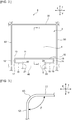
- Fig. 1 is a schematic cross-sectional view showing a transparent conductive film-equipped glass substrate according to one embodiment of the present invention.
- Fig. 2 is a schematic plan view showing the transparent conductive film-equipped glass substrate according to the one embodiment of the present invention.
- Fig. 1 is a schematic cross-sectional view taken along the line I-I shown in Fig. 2 .
- a transparent conductive film-equipped glass substrate 6 according to this embodiment includes a glass substrate 1, an underlying glass layer 2 provided on a principal surface 1a of the glass substrate 1, and a transparent conductive film 3 provided on a principal surface 2a of the underlying glass layer 2. Asperities are formed on the principal surface 1a of the glass substrate 1. Therefore, the underlying glass layer 2 is provided on the principal surface 1a having asperities formed thereon.
- a patterned region 10 formed by removing part of the transparent conductive film 3 by patterning using laser.
- the transparent conductive film 3 is divided by the patterned region 10 into a first electrode 4 and a second electrode 5.
- the transparent conductive film-equipped glass substrate 6 can be used, for example, as a glass substrate for an organic electroluminescent device.
- an organic electroluminescent layer is provided on the top of the transparent conductive film-equipped glass substrate 6.
- Light emitted from the organic electroluminescent layer due to the production of luminescence in the organic electroluminescent layer passes through the transparent conductive film 3 and the glass substrate 1 and is then extracted to the outside.
- the underlying glass layer 2 is provided between the transparent conductive film 3 and the glass substrate 1 in order to increase the extraction efficiency of light emitted from the organic electroluminescent layer.
- the organic electroluminescent layer has a refractive index nd of about 1.8 to 1.9
- the transparent conductive film 3 has a refractive index nd of about 1.9 to 2.0
- the glass substrate 1 normally has a refractive index nd of about 1.5. Therefore, if the underlying glass layer 2 is not provided, the difference in refractive index between the glass substrate 1 and the transparent conductive film 3 is large, so that light from the organic electroluminescent layer is reflected at the interface between the glass substrate 1 and the transparent conductive film 3 and thus cannot efficiently be extracted to the outside.
- the underlying glass layer 2 is generally made of a glass having a higher refractive index nd than the glass substrate 1, for example, having a refractive index of 1.8 to 2.2.
- a glass having a higher refractive index nd than the glass substrate 1, for example, having a refractive index of 1.8 to 2.2.
- Examples of such a glass include bismuth-based glasses.
- the bismuth-based glasses include glasses containing 10% by mole or more Bi 2 O 3 in a glass composition.
- compositions of the bismuth-based glasses include a glass containing, in % by mole, 10 to 35% Bi 2 O 3 , 20 to 35% B 2 O 3 , over 5 to 35% SiO 2 , 0 to 10% Al 2 O 3 , 0 to 10% ZnO, and 1 to 8% ZrO 2 , and a glass containing, in % by mole, 10 to 35% Bi 2 O 3 , 20 to 35% B 2 O 3 , 21 to 45% SiO 2 +Al 2 O 3 , 0 to 10% ZnO, and 0.1 to 10% ZrO 2 .
- SiO 2 +Al 2 O 3 means the sum of the contents of SiO 2 and Al 2 O 3 .
- the glass substrate 1 having asperities formed on the principal surface 1a thereof can be produced, for example, by subjecting a glass plate having a flat surface to processing, such as sandblasting, sol-gel spraying or etching.
- the above glass substrate can be produced by subjecting a glass plate to press forming using a die having asperities formed on the surface or by roll-forming molten glass using a roll having asperities formed on the surface.
- the surface roughness Ra of the principal surface 1a is, for example, preferably within a range of 0.05 to 2 ⁇ m and more preferably within a range of 0.05 to 1.5 ⁇ m. If the surface roughness Ra of the principal surface 1a is too small, a sufficient light extraction efficiently may not be able to be achieved. On the other hand, if the surface roughness Ra of the principal surface 1a is too large, a sufficient light extraction efficiently may not be able to be achieved and the thickness of the underlying glass layer 2 may have to be increased than necessary.
- the transparent conductive film 3 examples include thin films of composite oxides having electrical conductivity, such as indium tin oxides (ITO), aluminum zinc oxides (AZO), indium zinc oxides (IZO), and fluorine-doped tin oxides (FTO). Indium tin oxides are particularly preferably used.
- ITO indium tin oxides
- AZO aluminum zinc oxides
- IZO indium zinc oxides
- FTO fluorine-doped tin oxides
- Indium tin oxides are particularly preferably used.
- the transparent conductive film 3 is patterned by laser to remove part of the transparent conductive film 3, thus forming the patterned region 10.
- the laser that is used is a laser as to the wavelength of which the transparent conductive film 3 has a high absorptance.
- an ITO film exhibits high absorptance of wavelengths of 1000 nm or more. Therefore, the ITO film can be patterned using laser having a wavelength of 1000 nm or more to partly remove the ITO film by laser irradiation, thus forming a patterned region 10.
- the inventors have found that, during patterning by laser of the transparent conductive film 3 to remove part of the transparent conductive film 3 by laser irradiation, the transparent conductive film 3 or the underlying glass layer 2 may be discolored or damaged. They have found that such discoloration or damage is likely to occur particularly at corners at which the scanning direction of the laser changes to a perpendicular direction. They also have found from studies on the reason for this that when the laser scanning direction changes to a perpendicular direction, the scanning speed decreases, the laser irradiation time thus becomes relatively long, so that heat is accumulated at the portions to discolor or damage the portions. Furthermore, they have found that because the underlying glass layer 2 also has a high absorptance of the wavelength of the laser, the above phenomenon occurs.
- the underlying glass layer 2 has an absorptance of the wavelength of the laser lower than that of the transparent conductive film 3 and higher than that of the glass substrate 1.
- the absorptance of the underlying glass layer 2 as to the wavelength of the laser is preferably within a range of 10 to 60% of that of the transparent conductive film 3 and more preferably within a range of 10 to 30% thereof.
- the wavelength of the laser is, for example, preferably 1000 nm or more, more preferably 1300 nm or more, and still more preferably 1500 nm or more. No particular limitation is placed on the upper limit of the wavelength of the laser, but the wavelength of the laser is generally not more than 2000 nm.
- the laser is preferably sub-10-picosecond pulse laser, more preferably subpicosecond, ultrashort pulse laser, and particularly preferably laser laser.
- laser having such a short pulse width, a multiphoton absorption phenomenon is generated, so that patterning can be achieved without diffusing heat to the surrounding portions.
- the spot diameter of the laser is preferably within a range of 20% to 100% of the width of the patterned region and more preferably within a range of 50% to 100% thereof.
- the laser is generally applied in the direction of thickness of the transparent conductive film 3 (z direction) from the transparent conductive film 3 side.
- Fig. 2 is a schematic plan view showing the transparent conductive film-equipped glass substrate according to the one embodiment of the present invention.
- the transparent conductive film-equipped glass substrate 6 shown in Fig. 2 represents a patterned circuit of the transparent conductive film 3 corresponding to one organic electroluminescent device.
- the transparent conductive film-equipped glass substrate 6 shown in Fig. 2 is a piece of glass substrate of a mother glass substrate, in which other organic electroluminescent devices are formed next to the piece of glass substrate.
- linear patterned regions 30 and 40 are formed to extend in the x direction and linear patterned regions 50 and 60 are formed to extend in the y direction orthogonal to the linear patterned regions 30 and 40.
- the transparent conductive film 3 is separated from transparent conductive films of adjacent devices by the above patterned regions 30, 40, 50, and 60.
- the patterned region 10 shown in Fig. 1 is formed in the transparent conductive film 3.
- the transparent conductive film 3 is divided by the patterned region 10 to form a first electrode 4 and a second electrode 5.
- the first electrode 4 and the second electrode 5 can be used as an anode and a cathode, respectively.
- the second electrode can be connected to an electron-injection electrode provided on the top of the organic electroluminescent layer.
- the patterned region 10 includes a first linear portion 11 extending in the x direction and a second linear portion 12 extending in the y direction.
- the first linear portion 11 and the second linear portion 12 are connected by a connecting portion 13.
- the patterned region 10 further includes a second linear portion 14 extending in the y direction and the second linear portion 14 and the first linear portion 11 are connected by a connecting portion 15.
- the patterned region 10 also includes a first linear portion 16 extending in the x direction and the first linear portion 16 and the second linear portion 12 are connected by a connecting portion 17. Moreover, the patterned region 10 also includes a first linear portion 18 extending in the x direction and the first linear portion 18 and the second linear portion 14 are connected by a connecting portion 19.
- the patterned region 10 further includes a second linear portion 21 extending in the y direction and the second linear portion 21 and the first linear portion 16 are connected by a connecting portion 22. Furthermore, the patterned region 10 also includes a second linear portion 23 extending in the y direction and the second linear portion 23 and the first linear portion 18 are connected by a connecting portion 24.
- Fig. 3 is a schematic plan view showing on an enlarge scale the first linear portion 11, the second linear portion 12, and the connecting portion 13 shown in Fig. 2 .
- the first linear portion 11 and the second linear portion 12 are formed so that the angle formed between them is ⁇ .
- the angle ⁇ is 90°.
- the angle ⁇ formed by the first linear portion 11 and the second linear portion 12 in the present invention is not limited to the above and only has to be not more than 120°.
- the angle ⁇ formed by the first linear portion 11 and the second linear portion 12 is preferably within a range of 80° to 100°.
- the connecting portion 13 connecting between the first linear portion 11 and the second linear portion 12 is formed into an arc in this embodiment.
- the radius of curvature of the connecting portion 13 is 0.5 mm or more.
- the radius of curvature of the connecting portion 13 is preferably 1.0 mm or more. Since the radius of curvature of the connecting portion 13 is within the above range, the transparent conductive film 3 and the underlying glass layer 2 can be more effectively prevented from being discolored or damaged. If the radius of curvature of the connecting portion 13 is too large, the patterned region may be difficult to form. Therefore, the radius of curvature of the connecting portion 13 is preferably not more than 5.0 mm and more preferably not more than 3.0 mm.
- Fig. 4 is a schematic plan view showing on an enlarge scale a first linear portion 11, a second linear portion 12, and a connecting portion 34 in a comparative example.
- the connecting portion 34 connecting between the first linear portion 11 and the second linear portion 12 is not formed into an arc having a radius of curvature of 0.5 mm or more.
- the connecting portion 34, and the second linear portion 12 are scanned in this order by laser or the second linear portion 12, the connecting portion 34, and the first linear portion 11 are scanned in this order by laser, there arises a moment when the laser does not move at the connecting portion 34 in either the x direction or the y direction. Therefore, a site appears where the laser stays for a long time. Heat is accumulated in the site, so that the transparent conductive film 3 or the underlying glass layer 2 is discolored or damaged.
- the connecting portion 13 is formed into an arc having a radius of curvature of 0.5 mm or more, laser passes along the connecting portion 13 while always moving in at least either the x direction or the y direction and no site appears where the laser stays for a long time. Therefore, the transparent conductive film 3 and the underlying glass layer 2 can be prevented from being discolored or damaged.
- connecting portion 13 Although the description of the connecting portion 13 has been given with reference to Figs. 3 and 4 , the connecting portions 15, 17, 19, 22, and 24 shown in Fig. 2 , each formed into an arc having a radius of curvature of 0.5 mm or more, like the connecting portion 13, can prevent the transparent conductive film 3 or the underlying glass layer 2 from being discolored or damaged at these portions.
- linear portions extending in the x direction may be defined as first linear portions and the linear portions extending in the y direction may be defined as second linear portions.
Landscapes
- Engineering & Computer Science (AREA)
- Chemical & Material Sciences (AREA)
- Optics & Photonics (AREA)
- Physics & Mathematics (AREA)
- Materials Engineering (AREA)
- Organic Chemistry (AREA)
- Life Sciences & Earth Sciences (AREA)
- Chemical Kinetics & Catalysis (AREA)
- General Chemical & Material Sciences (AREA)
- Geochemistry & Mineralogy (AREA)
- Mechanical Engineering (AREA)
- Plasma & Fusion (AREA)
- Electroluminescent Light Sources (AREA)
- Surface Treatment Of Glass (AREA)
- Non-Insulated Conductors (AREA)
- Laser Beam Processing (AREA)
Abstract
Description
- The present invention relates to transparent conductive film-equipped glass substrates and methods for manufacturing the same.
- In relation to plasma displays, electroluminescent devices, and the like, it is known that a transparent conductive film for use as an electrode is formed on a transparent substrate, such as a glass substrate, and the transparent conductive film is subjected to patterning by laser (
Patent Literatures 1 and 2). - In the case of organic electroluminescent devices or the like, in order to increase the light extraction efficiency, an underlying glass layer having a higher refractive index than the glass substrate may be provided between the glass substrate and the transparent conductive film.
-
- [PTL 1]
JP-A-2007-207554 - [PTL 2]
JP-A-2006-267834 - The inventors have found a problem that when the underlying glass layer is provided, the transparent conductive film or the underlying glass layer is likely to be discolored or damaged during patterning of the transparent conductive film by laser.
- An object of the present invention is to provide a transparent conductive film-equipped glass substrate that, during patterning by laser of a transparent conductive film formed on an underlying glass layer, can prevent the transparent conductive film or the underlying glass layer from being discolored or damaged, and a manufacturing method thereof.
- A transparent conductive film-equipped glass substrate according to the present invention is a transparent conductive film-equipped glass substrate including a glass substrate, an underlying glass layer provided on the glass substrate, and a transparent conductive film provided on the underlying glass layer and subjected to patterning by laser, the underlying glass layer has an absorptance of a wavelength of the laser lower than the transparent conductive film and higher than the glass substrate, a patterned region formed by removing part of the transparent conductive film by the patterning by laser includes a first linear portion, a second linear portion, and a connecting portion connecting between the first linear portion and the second linear portion, the first linear portion and the second linear portion form an angle of 120° or less with each other, and the connecting portion has a radius of curvature of 0.5 mm or more.
- Examples of the underlying glass layer include those containing bismuth-based glass.
- Examples of the underlying glass layer include those having a higher refractive index than the glass substrate.
- An example of the laser that can be used is femtosecond laser.
- Asperities are preferably formed on a surface of the glass substrate on which the underlying glass layer is provided.
- The transparent conductive film-equipped glass substrate according to the present invention is used, for example, as a glass substrate for an organic electroluminescent device.
- A manufacturing method according to the present invention is a method that enables the manufacture of the above transparent conductive film-equipped glass substrate according to the present invention, the method including the steps of: producing the glass substrate on which the transparent conductive film before being subjected to the patterning is formed on the underlying glass layer; and applying the laser to the transparent conductive film to scan the first linear portion, the connecting portion, and the second linear portion in this order or reverse order with the laser, thus forming the patterned region.
- According to the present invention, during patterning by laser of a transparent conductive film formed on an underlying glass layer, the transparent conductive film and the underlying glass layer can be prevented from being discolored or damaged.
-
- [
Fig. 1 ]
Fig. 1 is a schematic cross-sectional view showing a transparent conductive film-equipped glass substrate according to one embodiment of the present invention. - [
Fig. 2 ]
Fig. 2 is a schematic plan view showing the transparent conductive film-equipped glass substrate according to the one embodiment of the present invention. - [
Fig. 3] Fig. 3 is a schematic plan view showing on an enlarge scale a first linear portion, a second linear portion, and a connecting portion shown inFig. 2 . - [
Fig. 4] Fig. 4 is a schematic plan view showing on an enlarge scale a first linear portion, a second linear portion, and a connecting portion in a comparative example. - Hereinafter, a description will be given of a preferred embodiment. However, the following embodiment is merely illustrative and the present invention is not limited to the following embodiment. Throughout the drawings, members having substantially the same functions may be referred to by the same reference characters.
-
Fig. 1 is a schematic cross-sectional view showing a transparent conductive film-equipped glass substrate according to one embodiment of the present invention.Fig. 2 is a schematic plan view showing the transparent conductive film-equipped glass substrate according to the one embodiment of the present invention.Fig. 1 is a schematic cross-sectional view taken along the line I-I shown inFig. 2 . As shown inFig. 1 , a transparent conductive film-equippedglass substrate 6 according to this embodiment includes aglass substrate 1, anunderlying glass layer 2 provided on aprincipal surface 1a of theglass substrate 1, and a transparentconductive film 3 provided on aprincipal surface 2a of theunderlying glass layer 2. Asperities are formed on theprincipal surface 1a of theglass substrate 1. Therefore, theunderlying glass layer 2 is provided on theprincipal surface 1a having asperities formed thereon. - Formed in the transparent
conductive film 3 is a patternedregion 10 formed by removing part of the transparentconductive film 3 by patterning using laser. The transparentconductive film 3 is divided by thepatterned region 10 into afirst electrode 4 and asecond electrode 5. - The transparent conductive film-equipped
glass substrate 6 according to this embodiment can be used, for example, as a glass substrate for an organic electroluminescent device. When it is used as a glass substrate for an organic electroluminescent device, an organic electroluminescent layer is provided on the top of the transparent conductive film-equippedglass substrate 6. Light emitted from the organic electroluminescent layer due to the production of luminescence in the organic electroluminescent layer passes through the transparentconductive film 3 and theglass substrate 1 and is then extracted to the outside. Theunderlying glass layer 2 is provided between the transparentconductive film 3 and theglass substrate 1 in order to increase the extraction efficiency of light emitted from the organic electroluminescent layer. - To be specific, generally, the organic electroluminescent layer has a refractive index nd of about 1.8 to 1.9, the transparent
conductive film 3 has a refractive index nd of about 1.9 to 2.0, and theglass substrate 1 normally has a refractive index nd of about 1.5. Therefore, if theunderlying glass layer 2 is not provided, the difference in refractive index between theglass substrate 1 and the transparentconductive film 3 is large, so that light from the organic electroluminescent layer is reflected at the interface between theglass substrate 1 and the transparentconductive film 3 and thus cannot efficiently be extracted to the outside. - When, as in this embodiment, the
underlying glass layer 2 is provided between theglass substrate 1 and the transparentconductive film 3 to bring the refractive index nd of theunderlying glass layer 2 close to the refractive index nd of the transparentconductive film 3, the above-mentioned light reflection can be reduced, so that the light can be efficiently extracted to the outside. Therefore, theunderlying glass layer 2 is generally made of a glass having a higher refractive index nd than theglass substrate 1, for example, having a refractive index of 1.8 to 2.2. Examples of such a glass include bismuth-based glasses. The bismuth-based glasses include glasses containing 10% by mole or more Bi2O3 in a glass composition. - Specific examples of compositions of the bismuth-based glasses include a glass containing, in % by mole, 10 to 35% Bi2O3, 20 to 35% B2O3, over 5 to 35% SiO2, 0 to 10% Al2O3, 0 to 10% ZnO, and 1 to 8% ZrO2, and a glass containing, in % by mole, 10 to 35% Bi2O3, 20 to 35% B2O3, 21 to 45% SiO2+Al2O3, 0 to 10% ZnO, and 0.1 to 10% ZrO2. Herein, "SiO2+Al2O3" means the sum of the contents of SiO2 and Al2O3.
- Furthermore, when, as in this embodiment, asperities are formed on the
principal surface 1a of theglass substrate 1, light reflection at the interface between theunderlying glass layer 2 and theglass substrate 1 can be reduced, so that the light can be more efficiently extracted to the outside. Theglass substrate 1 having asperities formed on theprincipal surface 1a thereof can be produced, for example, by subjecting a glass plate having a flat surface to processing, such as sandblasting, sol-gel spraying or etching. Alternatively, the above glass substrate can be produced by subjecting a glass plate to press forming using a die having asperities formed on the surface or by roll-forming molten glass using a roll having asperities formed on the surface. - The surface roughness Ra of the
principal surface 1a is, for example, preferably within a range of 0.05 to 2 µm and more preferably within a range of 0.05 to 1.5 µm. If the surface roughness Ra of theprincipal surface 1a is too small, a sufficient light extraction efficiently may not be able to be achieved. On the other hand, if the surface roughness Ra of theprincipal surface 1a is too large, a sufficient light extraction efficiently may not be able to be achieved and the thickness of theunderlying glass layer 2 may have to be increased than necessary. - Examples of the transparent
conductive film 3 that can be used include thin films of composite oxides having electrical conductivity, such as indium tin oxides (ITO), aluminum zinc oxides (AZO), indium zinc oxides (IZO), and fluorine-doped tin oxides (FTO). Indium tin oxides are particularly preferably used. - No particular limitation is placed on the type of the
glass substrate 1 so long as it does not reduce the light extraction efficiency. - In the present invention, the transparent
conductive film 3 is patterned by laser to remove part of the transparentconductive film 3, thus forming thepatterned region 10. The laser that is used is a laser as to the wavelength of which the transparentconductive film 3 has a high absorptance. For example, an ITO film exhibits high absorptance of wavelengths of 1000 nm or more. Therefore, the ITO film can be patterned using laser having a wavelength of 1000 nm or more to partly remove the ITO film by laser irradiation, thus forming a patternedregion 10. - As described previously, the inventors have found that, during patterning by laser of the transparent
conductive film 3 to remove part of the transparentconductive film 3 by laser irradiation, the transparentconductive film 3 or theunderlying glass layer 2 may be discolored or damaged. They have found that such discoloration or damage is likely to occur particularly at corners at which the scanning direction of the laser changes to a perpendicular direction. They also have found from studies on the reason for this that when the laser scanning direction changes to a perpendicular direction, the scanning speed decreases, the laser irradiation time thus becomes relatively long, so that heat is accumulated at the portions to discolor or damage the portions. Furthermore, they have found that because theunderlying glass layer 2 also has a high absorptance of the wavelength of the laser, the above phenomenon occurs. - Therefore, in the present invention, the
underlying glass layer 2 has an absorptance of the wavelength of the laser lower than that of the transparentconductive film 3 and higher than that of theglass substrate 1. The absorptance of theunderlying glass layer 2 as to the wavelength of the laser is preferably within a range of 10 to 60% of that of the transparentconductive film 3 and more preferably within a range of 10 to 30% thereof. - No particular limitation is placed on the wavelength of the laser so long as the transparent
conductive film 3 has a high absorptance of the wavelength. The wavelength of the laser is, for example, preferably 1000 nm or more, more preferably 1300 nm or more, and still more preferably 1500 nm or more. No particular limitation is placed on the upper limit of the wavelength of the laser, but the wavelength of the laser is generally not more than 2000 nm. - The laser is preferably sub-10-picosecond pulse laser, more preferably subpicosecond, ultrashort pulse laser, and particularly preferably laser laser. By the use of laser having such a short pulse width, a multiphoton absorption phenomenon is generated, so that patterning can be achieved without diffusing heat to the surrounding portions.
- The spot diameter of the laser is preferably within a range of 20% to 100% of the width of the patterned region and more preferably within a range of 50% to 100% thereof.
- The laser is generally applied in the direction of thickness of the transparent conductive film 3 (z direction) from the transparent
conductive film 3 side. -
Fig. 2 is a schematic plan view showing the transparent conductive film-equipped glass substrate according to the one embodiment of the present invention. The transparent conductive film-equippedglass substrate 6 shown inFig. 2 represents a patterned circuit of the transparentconductive film 3 corresponding to one organic electroluminescent device. The transparent conductive film-equippedglass substrate 6 shown inFig. 2 is a piece of glass substrate of a mother glass substrate, in which other organic electroluminescent devices are formed next to the piece of glass substrate. - As shown in
Fig. 2 , linearpatterned regions patterned regions patterned regions conductive film 3 is separated from transparent conductive films of adjacent devices by the abovepatterned regions - The patterned
region 10 shown inFig. 1 is formed in the transparentconductive film 3. The transparentconductive film 3 is divided by the patternedregion 10 to form afirst electrode 4 and asecond electrode 5. For example, thefirst electrode 4 and thesecond electrode 5 can be used as an anode and a cathode, respectively. The second electrode can be connected to an electron-injection electrode provided on the top of the organic electroluminescent layer. - As shown in
Fig. 2 , the patternedregion 10 includes a firstlinear portion 11 extending in the x direction and a secondlinear portion 12 extending in the y direction. The firstlinear portion 11 and the secondlinear portion 12 are connected by a connectingportion 13. The patternedregion 10 further includes a secondlinear portion 14 extending in the y direction and the secondlinear portion 14 and the firstlinear portion 11 are connected by a connectingportion 15. - Furthermore, the patterned
region 10 also includes a firstlinear portion 16 extending in the x direction and the firstlinear portion 16 and the secondlinear portion 12 are connected by a connectingportion 17. Moreover, the patternedregion 10 also includes a firstlinear portion 18 extending in the x direction and the firstlinear portion 18 and the secondlinear portion 14 are connected by a connectingportion 19. - The patterned
region 10 further includes a secondlinear portion 21 extending in the y direction and the secondlinear portion 21 and the firstlinear portion 16 are connected by a connectingportion 22. Furthermore, the patternedregion 10 also includes a secondlinear portion 23 extending in the y direction and the secondlinear portion 23 and the firstlinear portion 18 are connected by a connectingportion 24. -
Fig. 3 is a schematic plan view showing on an enlarge scale the firstlinear portion 11, the secondlinear portion 12, and the connectingportion 13 shown inFig. 2 . As shown inFig. 3 , the firstlinear portion 11 and the secondlinear portion 12 are formed so that the angle formed between them is θ. In this embodiment, the angle θ is 90°. The angle θ formed by the firstlinear portion 11 and the secondlinear portion 12 in the present invention is not limited to the above and only has to be not more than 120°. The angle θ formed by the firstlinear portion 11 and the secondlinear portion 12 is preferably within a range of 80° to 100°. - The connecting
portion 13 connecting between the firstlinear portion 11 and the secondlinear portion 12 is formed into an arc in this embodiment. In the present invention, the radius of curvature of the connectingportion 13 is 0.5 mm or more. The radius of curvature of the connectingportion 13 is preferably 1.0 mm or more. Since the radius of curvature of the connectingportion 13 is within the above range, the transparentconductive film 3 and theunderlying glass layer 2 can be more effectively prevented from being discolored or damaged. If the radius of curvature of the connectingportion 13 is too large, the patterned region may be difficult to form. Therefore, the radius of curvature of the connectingportion 13 is preferably not more than 5.0 mm and more preferably not more than 3.0 mm. -
Fig. 4 is a schematic plan view showing on an enlarge scale a firstlinear portion 11, a secondlinear portion 12, and a connectingportion 34 in a comparative example. In the comparative example shown inFig. 4 , the connectingportion 34 connecting between the firstlinear portion 11 and the secondlinear portion 12 is not formed into an arc having a radius of curvature of 0.5 mm or more. When in this case the firstlinear portion 11, the connectingportion 34, and the secondlinear portion 12 are scanned in this order by laser or the secondlinear portion 12, the connectingportion 34, and the firstlinear portion 11 are scanned in this order by laser, there arises a moment when the laser does not move at the connectingportion 34 in either the x direction or the y direction. Therefore, a site appears where the laser stays for a long time. Heat is accumulated in the site, so that the transparentconductive film 3 or theunderlying glass layer 2 is discolored or damaged. - In contrast, when as shown in
Fig. 3 the connectingportion 13 is formed into an arc having a radius of curvature of 0.5 mm or more, laser passes along the connectingportion 13 while always moving in at least either the x direction or the y direction and no site appears where the laser stays for a long time. Therefore, the transparentconductive film 3 and theunderlying glass layer 2 can be prevented from being discolored or damaged. - Although the description of the connecting
portion 13 has been given with reference toFigs. 3 and4 , the connectingportions Fig. 2 , each formed into an arc having a radius of curvature of 0.5 mm or more, like the connectingportion 13, can prevent the transparentconductive film 3 or theunderlying glass layer 2 from being discolored or damaged at these portions. - Although the description with reference to
Fig. 2 has been given by defining the linear portions extending in the x direction as first linear portions and defining the linear portions extending in the y direction as second linear portions, the present invention is not limited to this definition. The linear portions extending in the y direction may be defined as first linear portions and the linear portions extending in the x direction may be defined as second linear portions. -
- 1......glass substrate
- 1a......principal surface
- 2......underlying glass layer
- 2a......principal surface
- 3......transparent conductive film
- 4......first electrode
- 5......second electrode
- 6......transparent conductive film-equipped glass substrate
- 10, 30, 40, 50, 60......patterned region
- 11, 16, 18......first linear portion
- 12, 14, 21, 23......second linear portion
- 13, 15, 17, 19, 22, 24, 34......connecting portion
Claims (7)
- A transparent conductive film-equipped glass substrate including a glass substrate, an underlying glass layer provided on the glass substrate, and a transparent conductive film provided on the underlying glass layer and subjected to patterning by laser,
the underlying glass layer having an absorptance of a wavelength of the laser lower than the transparent conductive film and higher than the glass substrate,
wherein a patterned region formed by removing part of the transparent conductive film by the patterning by laser includes a first linear portion, a second linear portion, and a connecting portion connecting between the first linear portion and the second linear portion, the first linear portion and the second linear portion form an angle of 120° or less with each other, and the connecting portion has a radius of curvature of 0.5 mm or more. - The transparent conductive film-equipped glass substrate according to claim 1, wherein the underlying glass layer contains bismuth-based glass.
- The transparent conductive film-equipped glass substrate according to claim 1 or 2, wherein the underlying glass layer has a higher refractive index than the glass substrate.
- The transparent conductive film-equipped glass substrate according to any one of claims 1 to 3, wherein the laser is femtosecond laser.
- The transparent conductive film-equipped glass substrate according to any one of claims 1 to 4, wherein asperities are formed on a surface of the glass substrate on which the underlying glass layer is provided.
- The transparent conductive film-equipped glass substrate according to any one of claims 1 to 5, being a glass substrate for an organic electroluminescent device.
- A method for manufacturing the transparent conductive film-equipped glass substrate according to any one of claims 1 to 6, the method comprising the steps of:producing the glass substrate on which the transparent conductive film before being subjected to the patterning is formed on the underlying glass layer; andapplying the laser to the transparent conductive film to scan the first linear portion, the connecting portion, and the second linear portion in this order or reverse order with the laser, thus forming the patterned region.
Applications Claiming Priority (2)
| Application Number | Priority Date | Filing Date | Title |
|---|---|---|---|
| JP2015047169A JP6507729B2 (en) | 2015-03-10 | 2015-03-10 | Transparent conductive film-coated glass substrate and method of manufacturing the same |
| PCT/JP2016/050470 WO2016143366A1 (en) | 2015-03-10 | 2016-01-08 | Transparent conductive film-equipped glass substrate and method for manufacturing same |
Publications (3)
| Publication Number | Publication Date |
|---|---|
| EP3269689A1 true EP3269689A1 (en) | 2018-01-17 |
| EP3269689A4 EP3269689A4 (en) | 2018-11-14 |
| EP3269689B1 EP3269689B1 (en) | 2019-11-27 |
Family
ID=56880261
Family Applications (1)
| Application Number | Title | Priority Date | Filing Date |
|---|---|---|---|
| EP16761338.9A Active EP3269689B1 (en) | 2015-03-10 | 2016-01-08 | Transparent conductive film-equipped glass substrate and method for manufacturing same |
Country Status (7)
| Country | Link |
|---|---|
| US (1) | US10651404B2 (en) |
| EP (1) | EP3269689B1 (en) |
| JP (1) | JP6507729B2 (en) |
| KR (1) | KR20170125317A (en) |
| CN (1) | CN107406307A (en) |
| TW (1) | TWI672712B (en) |
| WO (1) | WO2016143366A1 (en) |
Families Citing this family (4)
| Publication number | Priority date | Publication date | Assignee | Title |
|---|---|---|---|---|
| US20220262929A1 (en) * | 2021-02-17 | 2022-08-18 | ColdQuanta, Inc. | Pulsed-laser modification of quantum-particle cells |
| US11997780B2 (en) | 2020-06-26 | 2024-05-28 | ColdQuanta, Inc. | Vacuum cell with electric-field control |
| DE102020133629A1 (en) | 2020-12-15 | 2022-06-15 | Trumpf Laser- Und Systemtechnik Gmbh | Process for joining at least two joining partners |
| CN114573246A (en) * | 2022-03-05 | 2022-06-03 | 安徽方兴光电新材料科技有限公司 | Double-sided laser-etchable conductive glass and preparation method thereof |
Family Cites Families (21)
| Publication number | Priority date | Publication date | Assignee | Title |
|---|---|---|---|---|
| US5432015A (en) * | 1992-05-08 | 1995-07-11 | Westaim Technologies, Inc. | Electroluminescent laminate with thick film dielectric |
| US5702656A (en) * | 1995-06-07 | 1997-12-30 | United States Surgical Corporation | Process for making polymeric articles |
| JP2001266654A (en) * | 2000-01-11 | 2001-09-28 | Sanyo Electric Co Ltd | Transparent electrode, method of patterning transparent electrode, and method of manufacturing semiconductor device using the same |
| JP4738860B2 (en) | 2005-03-25 | 2011-08-03 | 株式会社リコー | Electrochromic display element |
| DE602005019384D1 (en) * | 2005-04-21 | 2010-04-01 | Fiat Ricerche | Transparent LED display device |
| JP4872585B2 (en) * | 2005-12-06 | 2012-02-08 | 旭硝子株式会社 | Substrate with transparent conductive film for laser patterning and manufacturing method thereof |
| JP4803726B2 (en) * | 2006-02-01 | 2011-10-26 | 旭硝子株式会社 | Electronic circuit and manufacturing method thereof |
| TWI424479B (en) * | 2008-02-29 | 2014-01-21 | Ind Tech Res Inst | Method for patterning crystalline indium tin oxide by using femtosecond laser |
| KR20100138939A (en) * | 2008-03-18 | 2010-12-31 | 아사히 가라스 가부시키가이샤 | Electronic device board | substrate, laminated body for organic LED elements, its manufacturing method, organic LED element, and its manufacturing method |
| JP5239936B2 (en) * | 2009-02-23 | 2013-07-17 | 日本電気硝子株式会社 | Glass substrate for organic EL device and manufacturing method thereof |
| WO2011108494A1 (en) | 2010-03-01 | 2011-09-09 | Jsr株式会社 | Conductive laminate film and touch panel using the same |
| US8933906B2 (en) * | 2011-02-02 | 2015-01-13 | 3M Innovative Properties Company | Patterned substrates with non-linear conductor traces |
| JP2012170955A (en) * | 2011-02-17 | 2012-09-10 | Dainippon Screen Mfg Co Ltd | Pattern forming method |
| JP2014031310A (en) * | 2012-07-13 | 2014-02-20 | Nippon Electric Glass Co Ltd | Light extraction layer forming glass, and glass substrate for organic el element using the same |
| EP2712851B1 (en) * | 2012-09-28 | 2015-09-09 | Saint-Gobain Glass France | Method of producing a transparent diffusive oled substrate |
| US9368756B2 (en) * | 2012-10-12 | 2016-06-14 | Samsung Electronics Co., Ltd. | Organic electroluminescence device and method of manufacturing the same |
| JP6242800B2 (en) | 2012-10-19 | 2017-12-06 | ナミックス株式会社 | Sintered conductive paste |
| JP6327579B2 (en) * | 2013-02-07 | 2018-05-23 | 日本電気硝子株式会社 | Manufacturing method of glass substrate for organic EL element |
| WO2014181641A1 (en) * | 2013-05-09 | 2014-11-13 | 旭硝子株式会社 | Light-transmitting substrate, organic led element, and method for producing light-transmitting substrate |
| US20140347319A1 (en) | 2013-05-27 | 2014-11-27 | Wintek Corporation | Touch panel |
| TWI532560B (en) * | 2015-01-09 | 2016-05-11 | 位元奈米科技股份有限公司 | Laser etching method for transparent conductive plate and transparent conductive plate made thereof |
-
2015
- 2015-03-10 JP JP2015047169A patent/JP6507729B2/en not_active Expired - Fee Related
-
2016
- 2016-01-08 KR KR1020177013338A patent/KR20170125317A/en not_active Withdrawn
- 2016-01-08 EP EP16761338.9A patent/EP3269689B1/en active Active
- 2016-01-08 US US15/535,744 patent/US10651404B2/en not_active Expired - Fee Related
- 2016-01-08 WO PCT/JP2016/050470 patent/WO2016143366A1/en not_active Ceased
- 2016-01-08 CN CN201680014557.8A patent/CN107406307A/en active Pending
- 2016-01-18 TW TW105101411A patent/TWI672712B/en not_active IP Right Cessation
Also Published As
| Publication number | Publication date |
|---|---|
| EP3269689B1 (en) | 2019-11-27 |
| WO2016143366A1 (en) | 2016-09-15 |
| JP6507729B2 (en) | 2019-05-08 |
| JP2016166110A (en) | 2016-09-15 |
| KR20170125317A (en) | 2017-11-14 |
| US20180351116A1 (en) | 2018-12-06 |
| TW201633330A (en) | 2016-09-16 |
| CN107406307A (en) | 2017-11-28 |
| US10651404B2 (en) | 2020-05-12 |
| TWI672712B (en) | 2019-09-21 |
| EP3269689A4 (en) | 2018-11-14 |
Similar Documents
| Publication | Publication Date | Title |
|---|---|---|
| US10651404B2 (en) | Transparent conductive film-equipped glass substrate and method for manufacturing same | |
| US10290695B2 (en) | Display panel and fabrication method thereof | |
| CN113093445A (en) | Electroactive device and method of manufacturing an electroactive device | |
| RU2014121384A (en) | TRANSPARENT OSID DEVICE WITH A STRUCTURED CATHODE AND METHOD FOR PRODUCING SUCH ASID DEVICE | |
| EP3544936B1 (en) | Method for producing marked glass panels | |
| US9899462B2 (en) | Manufacturing method for OLED display panel | |
| JP2016532994A (en) | LAMINATE FOR LIGHT EMITTING DEVICE AND METHOD FOR MANUFACTURING THE SAME | |
| KR102381105B1 (en) | Substrate provided with transparent conductive film | |
| WO2013137403A1 (en) | Organic led element, light-transmitting substrate, and manufacturing method for light-transmitting substrate | |
| US9293707B2 (en) | Substrate with a functional layer comprising a sulphurous compound | |
| US10319934B2 (en) | Transparent supported electrode for OLED | |
| US10818869B2 (en) | Top-emitting type organic electroluminescent device, manufacturing method thereof and display apparatus | |
| CN102130308B (en) | Preparation method of substrate for increasing light output efficiency of organic light emitting device | |
| KR101470293B1 (en) | Method of fabricating light extraction substrate for oled | |
| KR20200029976A (en) | Transparent electrode | |
| US10453891B2 (en) | Substrate with conductive film | |
| US20260084246A1 (en) | Laser processing apparatus and method of manufacturing display device using the same | |
| JP2015088425A (en) | ORGANIC EL DEVICE, ITS MANUFACTURING METHOD, IMAGE DISPLAY DEVICE, AND LIGHTING DEVICE | |
| JP2016031860A (en) | Organic electroluminescence element and method of manufacturing transparent electrode plate | |
| US20200241412A1 (en) | Method for manufacturing optical member | |
| JP2014220217A (en) | Method for manufacturing electrode substrate for dye-sensitized solar cell |
Legal Events
| Date | Code | Title | Description |
|---|---|---|---|
| STAA | Information on the status of an ep patent application or granted ep patent |
Free format text: STATUS: THE INTERNATIONAL PUBLICATION HAS BEEN MADE |
|
| PUAI | Public reference made under article 153(3) epc to a published international application that has entered the european phase |
Free format text: ORIGINAL CODE: 0009012 |
|
| STAA | Information on the status of an ep patent application or granted ep patent |
Free format text: STATUS: REQUEST FOR EXAMINATION WAS MADE |
|
| 17P | Request for examination filed |
Effective date: 20170601 |
|
| AK | Designated contracting states |
Kind code of ref document: A1 Designated state(s): AL AT BE BG CH CY CZ DE DK EE ES FI FR GB GR HR HU IE IS IT LI LT LU LV MC MK MT NL NO PL PT RO RS SE SI SK SM TR |
|
| AX | Request for extension of the european patent |
Extension state: BA ME |
|
| DAV | Request for validation of the european patent (deleted) | ||
| DAX | Request for extension of the european patent (deleted) | ||
| A4 | Supplementary search report drawn up and despatched |
Effective date: 20181016 |
|
| RIC1 | Information provided on ipc code assigned before grant |
Ipc: C03C 17/34 20060101AFI20181010BHEP Ipc: C03C 3/064 20060101ALI20181010BHEP Ipc: H01L 51/50 20060101ALI20181010BHEP Ipc: B23K 26/351 20140101ALI20181010BHEP Ipc: H05B 33/02 20060101ALI20181010BHEP Ipc: H05B 33/28 20060101ALI20181010BHEP Ipc: H01L 51/00 20060101ALI20181010BHEP |
|
| STAA | Information on the status of an ep patent application or granted ep patent |
Free format text: STATUS: EXAMINATION IS IN PROGRESS |
|
| 17Q | First examination report despatched |
Effective date: 20190702 |
|
| GRAJ | Information related to disapproval of communication of intention to grant by the applicant or resumption of examination proceedings by the epo deleted |
Free format text: ORIGINAL CODE: EPIDOSDIGR1 |
|
| STAA | Information on the status of an ep patent application or granted ep patent |
Free format text: STATUS: GRANT OF PATENT IS INTENDED |
|
| GRAP | Despatch of communication of intention to grant a patent |
Free format text: ORIGINAL CODE: EPIDOSNIGR1 |
|
| INTG | Intention to grant announced |
Effective date: 20190904 |
|
| RIN1 | Information on inventor provided before grant (corrected) |
Inventor name: KASHIWADANI, KEN Inventor name: HIRAO, TORU Inventor name: WADA, MASANORI |
|
| GRAS | Grant fee paid |
Free format text: ORIGINAL CODE: EPIDOSNIGR3 |
|
| GRAA | (expected) grant |
Free format text: ORIGINAL CODE: 0009210 |
|
| STAA | Information on the status of an ep patent application or granted ep patent |
Free format text: STATUS: THE PATENT HAS BEEN GRANTED |
|
| AK | Designated contracting states |
Kind code of ref document: B1 Designated state(s): AL AT BE BG CH CY CZ DE DK EE ES FI FR GB GR HR HU IE IS IT LI LT LU LV MC MK MT NL NO PL PT RO RS SE SI SK SM TR |
|
| REG | Reference to a national code |
Ref country code: GB Ref legal event code: FG4D |
|
| REG | Reference to a national code |
Ref country code: CH Ref legal event code: EP |
|
| REG | Reference to a national code |
Ref country code: AT Ref legal event code: REF Ref document number: 1206492 Country of ref document: AT Kind code of ref document: T Effective date: 20191215 |
|
| REG | Reference to a national code |
Ref country code: DE Ref legal event code: R096 Ref document number: 602016025149 Country of ref document: DE |
|
| REG | Reference to a national code |
Ref country code: IE Ref legal event code: FG4D |
|
| REG | Reference to a national code |
Ref country code: NL Ref legal event code: MP Effective date: 20191127 |
|
| REG | Reference to a national code |
Ref country code: LT Ref legal event code: MG4D |
|
| PG25 | Lapsed in a contracting state [announced via postgrant information from national office to epo] |
Ref country code: LT Free format text: LAPSE BECAUSE OF FAILURE TO SUBMIT A TRANSLATION OF THE DESCRIPTION OR TO PAY THE FEE WITHIN THE PRESCRIBED TIME-LIMIT Effective date: 20191127 Ref country code: NL Free format text: LAPSE BECAUSE OF FAILURE TO SUBMIT A TRANSLATION OF THE DESCRIPTION OR TO PAY THE FEE WITHIN THE PRESCRIBED TIME-LIMIT Effective date: 20191127 Ref country code: GR Free format text: LAPSE BECAUSE OF FAILURE TO SUBMIT A TRANSLATION OF THE DESCRIPTION OR TO PAY THE FEE WITHIN THE PRESCRIBED TIME-LIMIT Effective date: 20200228 Ref country code: BG Free format text: LAPSE BECAUSE OF FAILURE TO SUBMIT A TRANSLATION OF THE DESCRIPTION OR TO PAY THE FEE WITHIN THE PRESCRIBED TIME-LIMIT Effective date: 20200227 Ref country code: FI Free format text: LAPSE BECAUSE OF FAILURE TO SUBMIT A TRANSLATION OF THE DESCRIPTION OR TO PAY THE FEE WITHIN THE PRESCRIBED TIME-LIMIT Effective date: 20191127 Ref country code: SE Free format text: LAPSE BECAUSE OF FAILURE TO SUBMIT A TRANSLATION OF THE DESCRIPTION OR TO PAY THE FEE WITHIN THE PRESCRIBED TIME-LIMIT Effective date: 20191127 Ref country code: NO Free format text: LAPSE BECAUSE OF FAILURE TO SUBMIT A TRANSLATION OF THE DESCRIPTION OR TO PAY THE FEE WITHIN THE PRESCRIBED TIME-LIMIT Effective date: 20200227 Ref country code: LV Free format text: LAPSE BECAUSE OF FAILURE TO SUBMIT A TRANSLATION OF THE DESCRIPTION OR TO PAY THE FEE WITHIN THE PRESCRIBED TIME-LIMIT Effective date: 20191127 |
|
| PG25 | Lapsed in a contracting state [announced via postgrant information from national office to epo] |
Ref country code: IS Free format text: LAPSE BECAUSE OF FAILURE TO SUBMIT A TRANSLATION OF THE DESCRIPTION OR TO PAY THE FEE WITHIN THE PRESCRIBED TIME-LIMIT Effective date: 20200327 Ref country code: HR Free format text: LAPSE BECAUSE OF FAILURE TO SUBMIT A TRANSLATION OF THE DESCRIPTION OR TO PAY THE FEE WITHIN THE PRESCRIBED TIME-LIMIT Effective date: 20191127 Ref country code: RS Free format text: LAPSE BECAUSE OF FAILURE TO SUBMIT A TRANSLATION OF THE DESCRIPTION OR TO PAY THE FEE WITHIN THE PRESCRIBED TIME-LIMIT Effective date: 20191127 |
|
| PG25 | Lapsed in a contracting state [announced via postgrant information from national office to epo] |
Ref country code: AL Free format text: LAPSE BECAUSE OF FAILURE TO SUBMIT A TRANSLATION OF THE DESCRIPTION OR TO PAY THE FEE WITHIN THE PRESCRIBED TIME-LIMIT Effective date: 20191127 |
|
| PG25 | Lapsed in a contracting state [announced via postgrant information from national office to epo] |
Ref country code: ES Free format text: LAPSE BECAUSE OF FAILURE TO SUBMIT A TRANSLATION OF THE DESCRIPTION OR TO PAY THE FEE WITHIN THE PRESCRIBED TIME-LIMIT Effective date: 20191127 Ref country code: CZ Free format text: LAPSE BECAUSE OF FAILURE TO SUBMIT A TRANSLATION OF THE DESCRIPTION OR TO PAY THE FEE WITHIN THE PRESCRIBED TIME-LIMIT Effective date: 20191127 Ref country code: RO Free format text: LAPSE BECAUSE OF FAILURE TO SUBMIT A TRANSLATION OF THE DESCRIPTION OR TO PAY THE FEE WITHIN THE PRESCRIBED TIME-LIMIT Effective date: 20191127 Ref country code: PT Free format text: LAPSE BECAUSE OF FAILURE TO SUBMIT A TRANSLATION OF THE DESCRIPTION OR TO PAY THE FEE WITHIN THE PRESCRIBED TIME-LIMIT Effective date: 20200419 Ref country code: EE Free format text: LAPSE BECAUSE OF FAILURE TO SUBMIT A TRANSLATION OF THE DESCRIPTION OR TO PAY THE FEE WITHIN THE PRESCRIBED TIME-LIMIT Effective date: 20191127 Ref country code: DK Free format text: LAPSE BECAUSE OF FAILURE TO SUBMIT A TRANSLATION OF THE DESCRIPTION OR TO PAY THE FEE WITHIN THE PRESCRIBED TIME-LIMIT Effective date: 20191127 |
|
| REG | Reference to a national code |
Ref country code: DE Ref legal event code: R097 Ref document number: 602016025149 Country of ref document: DE |
|
| PG25 | Lapsed in a contracting state [announced via postgrant information from national office to epo] |
Ref country code: SK Free format text: LAPSE BECAUSE OF FAILURE TO SUBMIT A TRANSLATION OF THE DESCRIPTION OR TO PAY THE FEE WITHIN THE PRESCRIBED TIME-LIMIT Effective date: 20191127 Ref country code: MC Free format text: LAPSE BECAUSE OF FAILURE TO SUBMIT A TRANSLATION OF THE DESCRIPTION OR TO PAY THE FEE WITHIN THE PRESCRIBED TIME-LIMIT Effective date: 20191127 Ref country code: SM Free format text: LAPSE BECAUSE OF FAILURE TO SUBMIT A TRANSLATION OF THE DESCRIPTION OR TO PAY THE FEE WITHIN THE PRESCRIBED TIME-LIMIT Effective date: 20191127 |
|
| REG | Reference to a national code |
Ref country code: CH Ref legal event code: PL |
|
| REG | Reference to a national code |
Ref country code: AT Ref legal event code: MK05 Ref document number: 1206492 Country of ref document: AT Kind code of ref document: T Effective date: 20191127 |
|
| PLBE | No opposition filed within time limit |
Free format text: ORIGINAL CODE: 0009261 |
|
| STAA | Information on the status of an ep patent application or granted ep patent |
Free format text: STATUS: NO OPPOSITION FILED WITHIN TIME LIMIT |
|
| REG | Reference to a national code |
Ref country code: BE Ref legal event code: MM Effective date: 20200131 |
|
| GBPC | Gb: european patent ceased through non-payment of renewal fee |
Effective date: 20200227 |
|
| PG25 | Lapsed in a contracting state [announced via postgrant information from national office to epo] |
Ref country code: LU Free format text: LAPSE BECAUSE OF NON-PAYMENT OF DUE FEES Effective date: 20200108 |
|
| 26N | No opposition filed |
Effective date: 20200828 |
|
| PG25 | Lapsed in a contracting state [announced via postgrant information from national office to epo] |
Ref country code: AT Free format text: LAPSE BECAUSE OF FAILURE TO SUBMIT A TRANSLATION OF THE DESCRIPTION OR TO PAY THE FEE WITHIN THE PRESCRIBED TIME-LIMIT Effective date: 20191127 Ref country code: PL Free format text: LAPSE BECAUSE OF FAILURE TO SUBMIT A TRANSLATION OF THE DESCRIPTION OR TO PAY THE FEE WITHIN THE PRESCRIBED TIME-LIMIT Effective date: 20191127 Ref country code: CH Free format text: LAPSE BECAUSE OF NON-PAYMENT OF DUE FEES Effective date: 20200131 Ref country code: SI Free format text: LAPSE BECAUSE OF FAILURE TO SUBMIT A TRANSLATION OF THE DESCRIPTION OR TO PAY THE FEE WITHIN THE PRESCRIBED TIME-LIMIT Effective date: 20191127 Ref country code: LI Free format text: LAPSE BECAUSE OF NON-PAYMENT OF DUE FEES Effective date: 20200131 Ref country code: BE Free format text: LAPSE BECAUSE OF NON-PAYMENT OF DUE FEES Effective date: 20200131 |
|
| PG25 | Lapsed in a contracting state [announced via postgrant information from national office to epo] |
Ref country code: IT Free format text: LAPSE BECAUSE OF FAILURE TO SUBMIT A TRANSLATION OF THE DESCRIPTION OR TO PAY THE FEE WITHIN THE PRESCRIBED TIME-LIMIT Effective date: 20191127 Ref country code: GB Free format text: LAPSE BECAUSE OF NON-PAYMENT OF DUE FEES Effective date: 20200227 Ref country code: IE Free format text: LAPSE BECAUSE OF NON-PAYMENT OF DUE FEES Effective date: 20200108 |
|
| PGFP | Annual fee paid to national office [announced via postgrant information from national office to epo] |
Ref country code: FR Payment date: 20211217 Year of fee payment: 7 |
|
| PGFP | Annual fee paid to national office [announced via postgrant information from national office to epo] |
Ref country code: DE Payment date: 20211130 Year of fee payment: 7 |
|
| PG25 | Lapsed in a contracting state [announced via postgrant information from national office to epo] |
Ref country code: TR Free format text: LAPSE BECAUSE OF FAILURE TO SUBMIT A TRANSLATION OF THE DESCRIPTION OR TO PAY THE FEE WITHIN THE PRESCRIBED TIME-LIMIT Effective date: 20191127 Ref country code: MT Free format text: LAPSE BECAUSE OF FAILURE TO SUBMIT A TRANSLATION OF THE DESCRIPTION OR TO PAY THE FEE WITHIN THE PRESCRIBED TIME-LIMIT Effective date: 20191127 Ref country code: CY Free format text: LAPSE BECAUSE OF FAILURE TO SUBMIT A TRANSLATION OF THE DESCRIPTION OR TO PAY THE FEE WITHIN THE PRESCRIBED TIME-LIMIT Effective date: 20191127 |
|
| PG25 | Lapsed in a contracting state [announced via postgrant information from national office to epo] |
Ref country code: MK Free format text: LAPSE BECAUSE OF FAILURE TO SUBMIT A TRANSLATION OF THE DESCRIPTION OR TO PAY THE FEE WITHIN THE PRESCRIBED TIME-LIMIT Effective date: 20191127 |
|
| REG | Reference to a national code |
Ref country code: DE Ref legal event code: R119 Ref document number: 602016025149 Country of ref document: DE |
|
| PG25 | Lapsed in a contracting state [announced via postgrant information from national office to epo] |
Ref country code: DE Free format text: LAPSE BECAUSE OF NON-PAYMENT OF DUE FEES Effective date: 20230801 |
|
| PG25 | Lapsed in a contracting state [announced via postgrant information from national office to epo] |
Ref country code: FR Free format text: LAPSE BECAUSE OF NON-PAYMENT OF DUE FEES Effective date: 20230131 |