EP3264578A1 - Discharging method of bus capacitor, controller, dc-dc convertrer and inverter - Google Patents
Discharging method of bus capacitor, controller, dc-dc convertrer and inverter Download PDFInfo
- Publication number
- EP3264578A1 EP3264578A1 EP17163273.0A EP17163273A EP3264578A1 EP 3264578 A1 EP3264578 A1 EP 3264578A1 EP 17163273 A EP17163273 A EP 17163273A EP 3264578 A1 EP3264578 A1 EP 3264578A1
- Authority
- EP
- European Patent Office
- Prior art keywords
- switch
- bus capacitor
- voltage
- turned
- preset condition
- Prior art date
- Legal status (The legal status is an assumption and is not a legal conclusion. Google has not performed a legal analysis and makes no representation as to the accuracy of the status listed.)
- Granted
Links
Images


Classifications
-
- H—ELECTRICITY
- H02—GENERATION; CONVERSION OR DISTRIBUTION OF ELECTRIC POWER
- H02M—APPARATUS FOR CONVERSION BETWEEN AC AND AC, BETWEEN AC AND DC, OR BETWEEN DC AND DC, AND FOR USE WITH MAINS OR SIMILAR POWER SUPPLY SYSTEMS; CONVERSION OF DC OR AC INPUT POWER INTO SURGE OUTPUT POWER; CONTROL OR REGULATION THEREOF
- H02M3/00—Conversion of DC power input into DC power output
- H02M3/02—Conversion of DC power input into DC power output without intermediate conversion into AC
- H02M3/04—Conversion of DC power input into DC power output without intermediate conversion into AC by static converters
- H02M3/10—Conversion of DC power input into DC power output without intermediate conversion into AC by static converters using discharge tubes with control electrode or semiconductor devices with control electrode
- H02M3/145—Conversion of DC power input into DC power output without intermediate conversion into AC by static converters using discharge tubes with control electrode or semiconductor devices with control electrode using devices of a triode or transistor type requiring continuous application of a control signal
- H02M3/155—Conversion of DC power input into DC power output without intermediate conversion into AC by static converters using discharge tubes with control electrode or semiconductor devices with control electrode using devices of a triode or transistor type requiring continuous application of a control signal using semiconductor devices only
- H02M3/156—Conversion of DC power input into DC power output without intermediate conversion into AC by static converters using discharge tubes with control electrode or semiconductor devices with control electrode using devices of a triode or transistor type requiring continuous application of a control signal using semiconductor devices only with automatic control of output voltage or current, e.g. switching regulators
- H02M3/158—Conversion of DC power input into DC power output without intermediate conversion into AC by static converters using discharge tubes with control electrode or semiconductor devices with control electrode using devices of a triode or transistor type requiring continuous application of a control signal using semiconductor devices only with automatic control of output voltage or current, e.g. switching regulators including plural semiconductor devices as final control devices for a single load
-
- H—ELECTRICITY
- H02—GENERATION; CONVERSION OR DISTRIBUTION OF ELECTRIC POWER
- H02M—APPARATUS FOR CONVERSION BETWEEN AC AND AC, BETWEEN AC AND DC, OR BETWEEN DC AND DC, AND FOR USE WITH MAINS OR SIMILAR POWER SUPPLY SYSTEMS; CONVERSION OF DC OR AC INPUT POWER INTO SURGE OUTPUT POWER; CONTROL OR REGULATION THEREOF
- H02M1/00—Details of apparatus for conversion
- H02M1/32—Means for protecting converters other than automatic disconnection
-
- H—ELECTRICITY
- H02—GENERATION; CONVERSION OR DISTRIBUTION OF ELECTRIC POWER
- H02M—APPARATUS FOR CONVERSION BETWEEN AC AND AC, BETWEEN AC AND DC, OR BETWEEN DC AND DC, AND FOR USE WITH MAINS OR SIMILAR POWER SUPPLY SYSTEMS; CONVERSION OF DC OR AC INPUT POWER INTO SURGE OUTPUT POWER; CONTROL OR REGULATION THEREOF
- H02M3/00—Conversion of DC power input into DC power output
- H02M3/02—Conversion of DC power input into DC power output without intermediate conversion into AC
- H02M3/04—Conversion of DC power input into DC power output without intermediate conversion into AC by static converters
- H02M3/10—Conversion of DC power input into DC power output without intermediate conversion into AC by static converters using discharge tubes with control electrode or semiconductor devices with control electrode
- H02M3/145—Conversion of DC power input into DC power output without intermediate conversion into AC by static converters using discharge tubes with control electrode or semiconductor devices with control electrode using devices of a triode or transistor type requiring continuous application of a control signal
- H02M3/155—Conversion of DC power input into DC power output without intermediate conversion into AC by static converters using discharge tubes with control electrode or semiconductor devices with control electrode using devices of a triode or transistor type requiring continuous application of a control signal using semiconductor devices only
- H02M3/156—Conversion of DC power input into DC power output without intermediate conversion into AC by static converters using discharge tubes with control electrode or semiconductor devices with control electrode using devices of a triode or transistor type requiring continuous application of a control signal using semiconductor devices only with automatic control of output voltage or current, e.g. switching regulators
- H02M3/158—Conversion of DC power input into DC power output without intermediate conversion into AC by static converters using discharge tubes with control electrode or semiconductor devices with control electrode using devices of a triode or transistor type requiring continuous application of a control signal using semiconductor devices only with automatic control of output voltage or current, e.g. switching regulators including plural semiconductor devices as final control devices for a single load
- H02M3/1582—Buck-boost converters
-
- H—ELECTRICITY
- H02—GENERATION; CONVERSION OR DISTRIBUTION OF ELECTRIC POWER
- H02M—APPARATUS FOR CONVERSION BETWEEN AC AND AC, BETWEEN AC AND DC, OR BETWEEN DC AND DC, AND FOR USE WITH MAINS OR SIMILAR POWER SUPPLY SYSTEMS; CONVERSION OF DC OR AC INPUT POWER INTO SURGE OUTPUT POWER; CONTROL OR REGULATION THEREOF
- H02M7/00—Conversion of AC power input into DC power output; Conversion of DC power input into AC power output
- H02M7/42—Conversion of DC power input into AC power output without possibility of reversal
- H02M7/44—Conversion of DC power input into AC power output without possibility of reversal by static converters
- H02M7/48—Conversion of DC power input into AC power output without possibility of reversal by static converters using discharge tubes with control electrode or semiconductor devices with control electrode
- H02M7/53—Conversion of DC power input into AC power output without possibility of reversal by static converters using discharge tubes with control electrode or semiconductor devices with control electrode using devices of a triode or transistor type requiring continuous application of a control signal
- H02M7/537—Conversion of DC power input into AC power output without possibility of reversal by static converters using discharge tubes with control electrode or semiconductor devices with control electrode using devices of a triode or transistor type requiring continuous application of a control signal using semiconductor devices only, e.g. single switched pulse inverters
-
- H—ELECTRICITY
- H02—GENERATION; CONVERSION OR DISTRIBUTION OF ELECTRIC POWER
- H02M—APPARATUS FOR CONVERSION BETWEEN AC AND AC, BETWEEN AC AND DC, OR BETWEEN DC AND DC, AND FOR USE WITH MAINS OR SIMILAR POWER SUPPLY SYSTEMS; CONVERSION OF DC OR AC INPUT POWER INTO SURGE OUTPUT POWER; CONTROL OR REGULATION THEREOF
- H02M1/00—Details of apparatus for conversion
- H02M1/32—Means for protecting converters other than automatic disconnection
- H02M1/322—Means for rapidly discharging a capacitor of the converter for protecting electrical components or for preventing electrical shock
Definitions
- the present disclosure relates to the technical field of power conversion, and in particular to a discharging method of a bus capacitor, a controller, a DC-DC converter and an inverter.
- a discharging resistor with a high resistance is directly connected in parallel to a bus capacitor. After powered off, the bus capacitor discharges continuously via the discharging resistor.
- a continuous discharge also occurs during operating of a system, which results in shortcomings of energy loss and low efficiency.
- insulation, heat dissipation and installation methods need to be taken into account.
- a switching unit In another conventional discharging circuit, a switching unit, a discharging unit connected to the bus capacitor via the switching unit, and a controlling unit connected to the switching unit are included.
- the controlling unit is configured to control, in a power-off state, the switching unit to be turned on to cause the discharging unit and the bus capacitor to form a discharging loop, and control, in a power-on state, the switching unit to be turned off.
- a discharging method of a bus capacitor, a controller, a DC-DC converter and an inverter are provided according to the present disclosure to solve the problem that an additional discharging circuit is required in the conventional technology.
- a discharging method of a bus capacitor is provided according to the present disclosure.
- the method is applied to a controller of a DC-DC converter or of an inverter.
- the DC-DC converter or the inverter includes a bus capacitor, a switch and a reactor.
- the discharging method of a bus capacitor includes:
- the determining whether the voltage across the bus capacitor meets a preset condition includes: determining whether the voltage across the bus capacitor is higher than or equal to a discharging threshold.
- the bus capacitor includes a first bus capacitor and a second bus capacitor
- the switch includes a first switch and a second switch connected in series, and a third switch and a fourth switch connected in series, and two series connection points are respectively connected to two terminals of the reactor; and the controlling, in a case that the voltage across the bus capacitor meets the preset condition, the switch to be turned on or turned off to cause the bus capacitor, the switch and the reactor to form a current loop, until the voltage across the bus capacitor does not meet the preset condition includes:
- the bus capacitor includes a first bus capacitor and a second bus capacitor
- the switch includes a first switch and a second switch connected in series, and a third switch and a fourth switch connected in series, and two series connection points are respectively connected to two terminals of the reactor; and the controlling, in a case that the voltage across the bus capacitor meets the preset condition, the switch to be turned on or turned off to cause the bus capacitor, the switch and the reactor to form a current loop, until the voltage across the bus capacitor does not meet the preset condition includes:
- a controller is provided according to the present disclosure.
- the controller is applied to a DC-DC converter or an inverter.
- the DC-DC converter or the inverter includes a bus capacitor, a switch and a reactor.
- the controller includes:
- the determining unit when the determining unit is configured to determine whether the voltage across the bus capacitor meets the preset condition, the determining unit is specifically configured to determine whether the voltage across the bus capacitor is higher than or equal to a discharging threshold.
- a DC-DC converter is provided according to the present disclosure.
- the DC-DC converter includes a first circuit breaker, a second circuit breaker, a first contactor, a second contactor, a first bus capacitor, a second bus capacitor, a first switch, a second switch, a third switch, a fourth switch, a reactor and the controller described above.
- the first switch, the second switch, the third switch and the fourth switch are each provided with an anti-parallel diode.
- An emitter of the first switch is connected to a collector of the second switch, and a connection point is connected to a terminal of the reactor.
- An emitter of the third switch is connected to a collector of the fourth switch, and a connection point is connected to the other terminal of the reactor.
- a collector of the first switch is connected to a terminal of the first bus capacitor and is connected to a positive electrode of a first terminal of the first circuit breaker via the first contactor.
- An emitter of the second switch is connected to the other terminal of the first bus capacitor and a negative electrode of the first terminal of the first circuit breaker.
- a collector of the third switch is connected to a terminal of the second bus capacitor and is connected to a positive electrode of a first terminal of the second circuit breaker via the second contactor.
- An emitter of the fourth switch is connected to the other terminal of the second bus capacitor and a negative electrode of the first terminal of the second circuit breaker.
- a first input terminal of the controller is connected to two terminals of the first bus capacitor, a second input terminal of the controller is connected to two terminals of the second bus capacitor, and an output terminal of the controller is connected to bases of the first switch, the second switch, the third switch and the fourth switch.
- the controlling unit of the controller when the controlling unit of the controller is configure to control, in a case that the voltage across the bus capacitor meets the preset condition, the switch to be turned on or turned off to cause the bus capacitor, the switch and the reactor to form the current loop, the controlling unit of the controller is specifically configured to:
- the controlling unit of the controller when the controlling unit of the controller is configure to control, in a case that the voltage across the bus capacitor meets the preset condition, the switch to be turned on or turned off to cause the bus capacitor, the switch and the reactor to form the current loop, the controlling unit of the controller is specifically configured to:
- the inverter is a three-phase full-bridge photovoltaic inverter, a three-phase full-bridge energy storage inverter, a multi-level photovoltaic inverter, or a multi-level energy storage inverter.
- the switch of the DC-DC converter or the inverter is controlled to be turned on or turned off to cause the bus capacitor, the switch and the reactor of the DC-DC converter or the inverter to form the current loop, until the voltage across the bus capacitor does not meet the preset condition.
- a discharging function is achieved for the bus capacitor after the DC-DC converter or the inverter is powered off, without the need for an additional discharging circuit, which solves the problems caused by the additional discharging circuit required in the conventional technology.
- a discharging method of a bus capacitor is provided according to the present disclosure to solve the problem that an additional discharging circuit is required in the conventional technology.
- the discharging method of a bus capacitor is applied to a controller of a DC-DC converter or of an inverter.
- the DC-DC converter or the inverter includes a bus capacitor, a switch and a reactor.
- the discharging method of a bus capacitor includes steps S101 to S103, as shown in Figure 1 .
- step S101 a voltage across the bus capacitor is detected.
- the voltage across the bus capacitor may be detected in a real-time manner. After the DC-DC converter or the inverter is powered off, there is residual power on the bus capacitor, and there is still a high voltage across the bus capacitor. In a case that there is no discharging circuit, theoretically, the voltage will remain. In practice, the voltage will decay slowly due to parasitic impedance of the bus, with a long discharging time. Therefore, the discharging method of a bus capacitor according to the embodiment may be applied to discharging of the bus capacitor.
- step S102 after the DC-DC converter or the inverter is powered off, whether the voltage across the bus capacitor meets a preset condition is determined.
- step S103 in a case that the voltage across the bus capacitor meets the preset condition, the switch is controlled to be turned on or turned off to cause the bus capacitor, the switch and the reactor to form a current loop, until the voltage across the bus capacitor does not meet the preset condition.
- the current loop may be formed by the bus capacitor and the reactor with the switch, and the residual power on the bus capacitor may be consumed in devices of the loop and in the circuit, via a power flow in the current loop, until the voltage across the bus capacitor does not meet the preset condition, thereby achieving discharging for the bus capacitor.
- a discharging function is achieved for the bus capacitor through the above steps without the need for an additional discharging circuit.
- no hardware component is added, and no additional loss is caused to normal operation of the circuit, avoiding problems in the conventional technology brought by a discharging resistor such as energy loss, low efficiency, and considerations of insulation, heat dissipation and installation methods.
- a barrier to a design trend of small volume and high density for a modular DC-DC converter is avoided. Therefore, the problems caused by an additional discharging circuit required in the conventional technology are solved.
- step S102 includes determining whether the voltage across the bus capacitor is higher than a discharging threshold.
- the discharging threshold may be 60V, which is not specifically limited herein and may be determined based on practical application environments.
- a detailed discharging method of a bus capacitor is further provided according to another embodiment of the present disclosure. That is, the discharging method of a bus capacitor is applied to a bi-directional DC-DC inverter shown in Figure 2 .
- the bus capacitor includes a first bus capacitor C1 and a second bus capacitor C2.
- the switch includes a first switch Q1 and a second switch Q2 connected in series, and a third switch Q3 and a fourth switch Q4 connected in series. Two series connection points are respectively connected to two terminals of the reactor L.
- step S103 includes:
- the controller After the bi-directional DC-DC converter is powered off, the controller detects the voltages across the first bus capacitor C1 and the second bus capacitor C2. In a case that the voltage V1 across the first bus capacitor C1 meets the preset condition (for example, V1 is higher than or equal to the discharging threshold of 60V), the controller controls the fourth switch Q4 to be turned on, and controls the first switch Q1 to be turned on in response to the first preset periodic pulse. Waveforms of turn-on control signals for the first switch Q1 and the fourth switch Q4 are shown in Figure 3 .
- the waveform of the turn-on control signal for the first switch Q1 is a continuous high level (as indicated by the dotted line in Figure 3 ), and the waveform of the turn-on control signal for the fourth switch Q4 is a pulse (as indicated by the solid line in Figure 3 ).
- the first switch Q1 In a case that the first switch Q1 is turned on, the first bus capacitor C1, the first switch Q1, the reactor L and the fourth switch Q4 form a current loop of a power flow, and a low forward current may flow through the reactor L.
- the first switch Q1 is turned on in response to the first preset periodic pulse, resulting in a short turn-on time of the first switch Q1 and a low current in the reactor L. Therefore, in a turn-off time of the first switch Q1, the current in the reactor L may decay to zero or near zero due to turn-on loss of diodes and line impedances, which avoids net increase of the current in the reactor L during a switching period, and thus avoids that the current in the reactor L becomes uncontrollable after multiple switching periods. In this way, after multiple switching periods, the voltage V1 across the first bus capacitor C1 decreases below the discharging threshold, and the controller can stop the discharging of the first bus capacitor C1.
- the discharge principle of the second bus capacitor C2 is the same as that of the first bus capacitor C1 described above, which is not described herein.
- the discharging method of a bus capacitor is applied to a bi-directional DC-DC inverter shown in Figure 2 .
- the bus capacitor includes a first bus capacitor C1 and a second bus capacitor C2.
- the switch includes a first switch Q1 and a second switch Q2 connected in series, and a third switch Q3 and a fourth switch Q4 connected in series. Two series connection points are respectively connected to two terminals of the reactor L.
- Step S103 includes:
- the controller controls, the switch group of the first switch Q1 and the fourth switch Q4 and the switch group of the second switch Q2 and the third switch Q3, to be alternately turned on or turned off.
- the first switch Q1 and the fourth switch Q4 are turned on or turned off simultaneously, and the second switch Q2 and the third switch Q3 are turned on or turned off simultaneously.
- the first switch Q1 and the fourth switch Q4 are simultaneously turned on, the first bus capacitor C1, the reactor L, the first switch Q1 and the fourth switch Q4 form a current loop of a power, and a current in the reactor L increases in the forward direction.
- the current in the reactor L freewheels, and charges the second bus capacitor C2 via the anti-parallel diodes of the second switch Q2 and the third switch Q3.
- the controller controls the first switch Q1 and the fourth switch Q4 to be turned on in response to the second preset periodic pulse, and may control a turn-on time of the first switch Q1 and the fourth switch Q4 to be short.
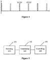
- the current in the reactor L may quickly decay to zero or near zero. Waveforms of turn-on control signals for the switches are shown in Figure 4 which takes a case that the first switch Q1 and the fourth switch Q4 are turned on firstly as an example for illustration.
- the pulses, sequence numbers of which are odd, are the turn-on control signals for the first switch Q1 and the fourth switch Q4 (as indicated by the thick dash line in Figure 4 ).
- the pulses, sequence numbers of which are even, are the turn-on control signals for the second switch Q2 and the third switch Q3 (as indicated by the thin solid line in Figure 4 ).
- the switch group of the second switch Q2 and the third switch Q3 is turned on or turned off.
- the second switch Q2 and the third switch Q3 are simultaneously turned on, the second bus capacitor C2, the reactor L, the second switch Q2 and the third switch Q3 form a current loop of a power, and a current in the reactor L increases in the reverse direction.
- the current in the reactor L freewheels, and charges the first bus capacitor C1 via the anti-parallel diodes of the first switch Q1 and the fourth switch Q4.
- the controller controls the second switch Q2 and the third switch Q3 to be turned on in response to the second preset periodic pulse, and may control a turn-on time of the second switch Q2 and the third switch Q3 to be short.
- the current in the reactor L may quickly decay to zero or near zero.
- Power loss may occur in turn-on and turn-off processes of the switches and in the process of forming the power flow described above.
- the controller can stop discharging of the first bus capacitor C 1 and the second bus capacitor C2.
- a controller is further provided according to another embodiment of the present disclosure, which is applied to a DC-DC converter or an inverter.
- the DC-DC converter or the inverter includes a bus capacitor, a switch and a reactor. As shown in Figure 5 , the controller includes:
- a discharging function can be achieved for the bus capacitor by the above principles, without the need for an additional discharging circuit, which avoids problems in the conventional technology brought by a discharging resistor such as energy loss, low efficiency, and considerations of insulation, heat dissipation and installation methods.
- a barrier to a design trend of small volume and high density for a modular DC-DC converter is avoided. Therefore, the problems caused by an additional discharging circuit required in the conventional technology are solved.
- the controller When the controller is applied to the DC-DC converter or the inverter, the controller may be a separate control part, or may be integrated in an original controller of the DC-DC converter or the inverter, which is not specifically limited herein. Both of the above cases fall within the protection scope of the present disclosure.
- the determining unit 102 when the determining unit 102 is configured to determine whether the voltage across the bus capacitor meets the preset condition, the determining unit 102 is specifically configured to determine whether the voltage across the bus capacitor is higher than a discharging threshold.
- the discharging threshold may be 60V, which is not specifically limited herein and may be determined based on practical application environments.
- a DC-DC converter is further provided according to another embodiment of the present disclosure, as shown in Figure 2 .
- the DC-DC converter includes a first circuit breaker, a second circuit breaker, a first contactor K1, a second contactor K2, a first bus capacitor C1, a second bus capacitor C2, a first switch Q1, a second switch Q2, a third switch Q3, a fourth switch Q4, a reactor L and the controller according to the above embodiments.
- the first switch Q1, the second switch Q2, the third switch Q3 and the fourth switch Q4 are each provided with an anti-parallel diode.
- An emitter of the first switch Q1 is connected to a collector of the second switch Q2, and a connection point is connected to a terminal of the reactor L.
- An emitter of the third switch Q3 is connected to a collector of the fourth switch Q4, and a connection point is connected to the other terminal of the reactor L.
- a collector of the first switch Q1 is connected to a terminal of the first bus capacitor C 1 and is connected to a positive electrode of a first terminal of the first circuit breaker via the first contactor K1.
- An emitter of the second switch Q2 is connected to the other terminal of the first bus capacitor C1 and a negative electrode of the first terminal of the first circuit breaker.
- a collector of the third switch Q3 is connected to a terminal of the second bus capacitor C2 and is connected to a positive electrode of a first terminal of the second circuit breaker via the second contactor K2.
- An emitter of the fourth switch Q4 is connected to the other terminal of the second bus capacitor C2 and a negative electrode of the first terminal of the second circuit breaker.
- a first input terminal of the controller is connected to two terminals of the first bus capacitor C1, a second input terminal of the controller is connected to two terminals of the second bus capacitor C2, and an output terminal of the controller is connected to bases of the first switch Q1, the second switch Q2, the third switch Q3 and the fourth switch Q4.
- the first switch Q1 is a forward BUCK switch
- the second switch Q2 is a reverse BOOST switch
- the third switch Q3 is a reverse BUCK switch
- the fourth switch Q4 is a forward BOOST switch, which makes the DC-DC converter achieve bi-directional DC-DC conversion. That is, the DC-DC converter shown in Figure 2 is a bi-directional DC-DC converter.
- the controller according to the above embodiments is provided. After the DC-DC converter is powered off, a discharging function can be achieved for the bus capacitor by the above principles, without the need for an additional discharging circuit, which avoids problems in the conventional technology brought by a discharging resistor such as energy loss, low efficiency, and considerations of insulation, heat dissipation and installation methods. In addition, a barrier to a design trend of small volume and high density for a modular DC-DC converter is avoided. Therefore, the problems caused by an additional discharging circuit required in the conventional technology are solved.
- the controlling unit of the controller when the controlling unit of the controller is configure to control, in a case that the voltage across the bus capacitor meets the preset condition, the switch to be turned on or turned off to cause the bus capacitor, the switch and the reactor to form the current loop, the controlling unit of the controller is specifically configured to:
- the controlling unit of the controller when the controlling unit of the controller is configure to control, in a case that the voltage across the bus capacitor meets the preset condition, the switch to be turned on or turned off to cause the bus capacitor, the switch and the reactor to form the current loop, the controlling unit of the controller is specifically configured to:
- An inverter is further provided according to another embodiment of the present disclosure, which includes the controller described above.
- the inverter is a three-phase full-bridge photovoltaic inverter, a three-phase full-bridge energy storage inverter, a multi-level photovoltaic inverter, or a multi-level energy storage inverter.
Landscapes
- Engineering & Computer Science (AREA)
- Power Engineering (AREA)
- Dc-Dc Converters (AREA)
Abstract
Description
- The present disclosure relates to the technical field of power conversion, and in particular to a discharging method of a bus capacitor, a controller, a DC-DC converter and an inverter.
- Presently, after various DC-DC converters or inverters power off, electric energy stored in a direct current bus capacitor needs to be discharged via an additional discharging circuit, otherwise, the waiting time for discharging is very long, thus leading to safety concern.
- In a conventional discharging circuit, a discharging resistor with a high resistance is directly connected in parallel to a bus capacitor. After powered off, the bus capacitor discharges continuously via the discharging resistor. However, such a continuous discharge also occurs during operating of a system, which results in shortcomings of energy loss and low efficiency. In addition, for the discharging resistor connected in parallel to the high-voltage bus, insulation, heat dissipation and installation methods need to be taken into account.
- In another conventional discharging circuit, a switching unit, a discharging unit connected to the bus capacitor via the switching unit, and a controlling unit connected to the switching unit are included. The controlling unit is configured to control, in a power-off state, the switching unit to be turned on to cause the discharging unit and the bus capacitor to form a discharging loop, and control, in a power-on state, the switching unit to be turned off. When this type of discharging circuit is applied in a high-voltage DC-DC converter, two of the discharging circuits are required, resulting a high hardware cost, and a large structural space being occupied. Therefore, a barrier to a design trend of small volume and high density is formed for a modular DC-DC converter.
- In view of the above problems, it is urgent to provide a discharging method of a bus capacitor without the need for an additional discharging circuit.
- In view of the above, a discharging method of a bus capacitor, a controller, a DC-DC converter and an inverter are provided according to the present disclosure to solve the problem that an additional discharging circuit is required in the conventional technology.
- To achieve the above object, the following technical solutions are provided according to the present disclosure.
- A discharging method of a bus capacitor is provided according to the present disclosure. The method is applied to a controller of a DC-DC converter or of an inverter. The DC-DC converter or the inverter includes a bus capacitor, a switch and a reactor. The discharging method of a bus capacitor includes:
- detecting a voltage across the bus capacitor;
- determining whether the voltage across the bus capacitor meets a preset condition, after the DC-DC converter or the inverter is powered off; and
- controlling, in a case that the voltage across the bus capacitor meets the preset condition, the switch to be turned on or turned off to cause the bus capacitor, the switch and the reactor to form a current loop, until the voltage across the bus capacitor does not meet the preset condition.
- Preferably, the determining whether the voltage across the bus capacitor meets a preset condition includes: determining whether the voltage across the bus capacitor is higher than or equal to a discharging threshold.
- Preferably, in a case that the discharging method of a bus capacitor is applied to a bi-directional DC-DC converter, the bus capacitor includes a first bus capacitor and a second bus capacitor, the switch includes a first switch and a second switch connected in series, and a third switch and a fourth switch connected in series, and two series connection points are respectively connected to two terminals of the reactor; and
the controlling, in a case that the voltage across the bus capacitor meets the preset condition, the switch to be turned on or turned off to cause the bus capacitor, the switch and the reactor to form a current loop, until the voltage across the bus capacitor does not meet the preset condition includes: - controlling, in a case that a voltage across the first bus capacitor meets the preset condition, the fourth switch to be turned on, and controlling the first switch to be turned on in response to a first preset periodic pulse, until the voltage across the first bus capacitor does not meet the preset condition; and
- controlling, in a case that a voltage across the second bus capacitor meets the preset condition, the second switch to be turned on, and controlling the third switch to be turned on in response to the first preset periodic pulse, until the voltage across the second bus capacitor does not meet the preset condition.
- Preferably, in a case that the discharging method of a bus capacitor is applied to a bi-directional DC-DC converter, the bus capacitor includes a first bus capacitor and a second bus capacitor, the switch includes a first switch and a second switch connected in series, and a third switch and a fourth switch connected in series, and two series connection points are respectively connected to two terminals of the reactor; and
the controlling, in a case that the voltage across the bus capacitor meets the preset condition, the switch to be turned on or turned off to cause the bus capacitor, the switch and the reactor to form a current loop, until the voltage across the bus capacitor does not meet the preset condition includes: - controlling, in a case that a voltage across the first bus capacitor and/or a voltage across the second bus capacitor meet the preset condition, two switch groups to be alternately turned on or turned off in response to a second preset periodic pulse, until neither the voltage across the first bus capacitor nor the voltage across the second bus capacitor meets the preset condition; where one of the two switch groups includes the first switch and the fourth switch that are simultaneously turned on or turned off, and the other of the two switch groups includes the second switch and the third switch that are simultaneously turned on or turned off.
- A controller is provided according to the present disclosure. The controller is applied to a DC-DC converter or an inverter. The DC-DC converter or the inverter includes a bus capacitor, a switch and a reactor. The controller includes:
- a detecting unit, configured to detect a voltage across the bus capacitor, after the DC-DC converter or the inverter is powered off;
- a determining unit, configured to determine whether the voltage across the bus capacitor meets a preset condition; and
- a controlling unit, configured to control, in a case that the voltage across the bus capacitor meets the preset condition, the switch to be turned on or turned off to cause the bus capacitor, the switch and the reactor to form a current loop, until the voltage across the bus capacitor does not meet the preset condition.
- Preferably, when the determining unit is configured to determine whether the voltage across the bus capacitor meets the preset condition, the determining unit is specifically configured to determine whether the voltage across the bus capacitor is higher than or equal to a discharging threshold.
- A DC-DC converter is provided according to the present disclosure. The DC-DC converter includes a first circuit breaker, a second circuit breaker, a first contactor, a second contactor, a first bus capacitor, a second bus capacitor, a first switch, a second switch, a third switch, a fourth switch, a reactor and the controller described above.
- The first switch, the second switch, the third switch and the fourth switch are each provided with an anti-parallel diode.
- An emitter of the first switch is connected to a collector of the second switch, and a connection point is connected to a terminal of the reactor.
- An emitter of the third switch is connected to a collector of the fourth switch, and a connection point is connected to the other terminal of the reactor.
- A collector of the first switch is connected to a terminal of the first bus capacitor and is connected to a positive electrode of a first terminal of the first circuit breaker via the first contactor.
- An emitter of the second switch is connected to the other terminal of the first bus capacitor and a negative electrode of the first terminal of the first circuit breaker.
- A collector of the third switch is connected to a terminal of the second bus capacitor and is connected to a positive electrode of a first terminal of the second circuit breaker via the second contactor.
- An emitter of the fourth switch is connected to the other terminal of the second bus capacitor and a negative electrode of the first terminal of the second circuit breaker.
- A first input terminal of the controller is connected to two terminals of the first bus capacitor, a second input terminal of the controller is connected to two terminals of the second bus capacitor, and an output terminal of the controller is connected to bases of the first switch, the second switch, the third switch and the fourth switch.
- Preferably, when the controlling unit of the controller is configure to control, in a case that the voltage across the bus capacitor meets the preset condition, the switch to be turned on or turned off to cause the bus capacitor, the switch and the reactor to form the current loop, the controlling unit of the controller is specifically configured to:
- control, in a case that a voltage across the first bus capacitor meets the preset condition, the fourth switch to be turned on, and control the first switch to be turned on in response to a first preset periodic pulse, until the voltage across the first bus capacitor does not meet the preset condition; and
- control, in a case that a voltage across the second bus capacitor meets the preset condition, the second switch to be turned on, and control the third switch to be turned on in response to the first preset periodic pulse, until the voltage across the second bus capacitor does not meet the preset condition.
- Preferably, when the controlling unit of the controller is configure to control, in a case that the voltage across the bus capacitor meets the preset condition, the switch to be turned on or turned off to cause the bus capacitor, the switch and the reactor to form the current loop, the controlling unit of the controller is specifically configured to:
- control, in a case that a voltage across the first bus capacitor and/or a voltage across the second bus capacitor meet the preset condition, two switch groups to be alternately turned on or turned off in response to a second preset periodic pulse, until neither the voltage across the first bus capacitor nor the voltage across the second bus capacitor meets the preset condition, where one of the two switch groups includes the first switch and the fourth switch that are simultaneously turned on or turned off, and the other of the two switch groups includes the second switch and the third switch that are simultaneously turned on or turned off.
- An inverter including the controller described above is provided according to the present disclosure. The inverter is a three-phase full-bridge photovoltaic inverter, a three-phase full-bridge energy storage inverter, a multi-level photovoltaic inverter, or a multi-level energy storage inverter.
- In the discharging method of a bus capacitor according to the present disclosure, after the DC-DC converter or the inverter is powered off, in a case that the detected voltage across the bus capacitor of the DC-DC converter or the inverter is determined to meet the preset condition, the switch of the DC-DC converter or the inverter is controlled to be turned on or turned off to cause the bus capacitor, the switch and the reactor of the DC-DC converter or the inverter to form the current loop, until the voltage across the bus capacitor does not meet the preset condition. Based on the method, a discharging function is achieved for the bus capacitor after the DC-DC converter or the inverter is powered off, without the need for an additional discharging circuit, which solves the problems caused by the additional discharging circuit required in the conventional technology.
- To illustrate technical solutions in embodiments of the present disclosure or in the conventional technology more clearly, drawings used in the descriptions of the embodiments or the conventional technology are introduced briefly hereinafter. Apparently, the drawings described hereinafter merely illustrate some embodiments of the present disclosure, and other drawings may be obtained by those skilled in the art based on those drawings without any creative efforts.
-
Figure 1 is a flow chart of a discharging method of a bus capacitor according to an embodiment of the present disclosure; -
Figure 2 is a schematic diagram of a circuit of a DC-DC inverter according to an embodiment of the present disclosure; -
Figure 3 is a waveform diagram of a turn-on control signal for a switch according to an embodiment of the present disclosure; -
Figure 4 is a waveform diagram of turn-on control signals for switches according to another embodiment of the present disclosure; and -
Figure 5 is a schematic structural diagram of a controller according to an embodiment of the present disclosure. - Technical solutions in embodiments of the present disclosure are clearly and completely described hereinafter in conjunction with the drawings of the embodiments of the present disclosure. Apparently, the described embodiments are only a few rather than all of the embodiments of the invention. All other embodiments obtained by those skilled in the art based on the embodiments of the present disclosure without any creative efforts fall within the protection scope of the present disclosure.
- A discharging method of a bus capacitor is provided according to the present disclosure to solve the problem that an additional discharging circuit is required in the conventional technology.
- The discharging method of a bus capacitor is applied to a controller of a DC-DC converter or of an inverter. The DC-DC converter or the inverter includes a bus capacitor, a switch and a reactor. The discharging method of a bus capacitor includes steps S101 to S103, as shown in
Figure 1 . - In step S101, a voltage across the bus capacitor is detected.
- In practical applications, the voltage across the bus capacitor may be detected in a real-time manner. After the DC-DC converter or the inverter is powered off, there is residual power on the bus capacitor, and there is still a high voltage across the bus capacitor. In a case that there is no discharging circuit, theoretically, the voltage will remain. In practice, the voltage will decay slowly due to parasitic impedance of the bus, with a long discharging time. Therefore, the discharging method of a bus capacitor according to the embodiment may be applied to discharging of the bus capacitor.
- In step S102, after the DC-DC converter or the inverter is powered off, whether the voltage across the bus capacitor meets a preset condition is determined.
- After the voltage across the bus capacitor is detected, whether the voltage across the bus capacitor meets the preset condition is determined to obtain a result of whether discharge is required.
- In step S103, in a case that the voltage across the bus capacitor meets the preset condition, the switch is controlled to be turned on or turned off to cause the bus capacitor, the switch and the reactor to form a current loop, until the voltage across the bus capacitor does not meet the preset condition.
- In a case that the voltage across the bus capacitor meets the preset condition, it is indicated that the bus capacitor requires discharging, otherwise, a potential hazard may be caused. Specifically, the current loop may be formed by the bus capacitor and the reactor with the switch, and the residual power on the bus capacitor may be consumed in devices of the loop and in the circuit, via a power flow in the current loop, until the voltage across the bus capacitor does not meet the preset condition, thereby achieving discharging for the bus capacitor.
- In the discharging method of a bus capacitor according to the embodiment, after the DC-DC converter or the inverter is powered off, a discharging function is achieved for the bus capacitor through the above steps without the need for an additional discharging circuit. As a result, no hardware component is added, and no additional loss is caused to normal operation of the circuit, avoiding problems in the conventional technology brought by a discharging resistor such as energy loss, low efficiency, and considerations of insulation, heat dissipation and installation methods. In addition, a barrier to a design trend of small volume and high density for a modular DC-DC converter is avoided. Therefore, the problems caused by an additional discharging circuit required in the conventional technology are solved.
- Preferably, step S102 includes determining whether the voltage across the bus capacitor is higher than a discharging threshold.
- For a bi-directional DC-DC converter, the discharging threshold may be 60V, which is not specifically limited herein and may be determined based on practical application environments.
- A detailed discharging method of a bus capacitor is further provided according to another embodiment of the present disclosure. That is, the discharging method of a bus capacitor is applied to a bi-directional DC-DC inverter shown in
Figure 2 . The bus capacitor includes a first bus capacitor C1 and a second bus capacitor C2. The switch includes a first switch Q1 and a second switch Q2 connected in series, and a third switch Q3 and a fourth switch Q4 connected in series. Two series connection points are respectively connected to two terminals of the reactor L. - On the basis of
Figure 1 , step S103 includes: - controlling, in a case that a voltage across the first bus capacitor meets the preset condition, the fourth switch to be turned on, and controlling the first switch to be turned on in response to a first preset periodic pulse, until the voltage across the first bus capacitor does not meet the preset condition; and
- controlling, in a case that a voltage across the second bus capacitor meets the preset condition, the second switch to be turned on, and controlling the third switch to be turned on in response to the first preset periodic pulse, until the voltage across the second bus capacitor does not meet the preset condition.
- Specifically, reference is made to
Figure 2 . After the bi-directional DC-DC converter is powered off, the controller detects the voltages across the first bus capacitor C1 and the second bus capacitor C2. In a case that the voltage V1 across the first bus capacitor C1 meets the preset condition (for example, V1 is higher than or equal to the discharging threshold of 60V), the controller controls the fourth switch Q4 to be turned on, and controls the first switch Q1 to be turned on in response to the first preset periodic pulse. Waveforms of turn-on control signals for the first switch Q1 and the fourth switch Q4 are shown inFigure 3 . The waveform of the turn-on control signal for the first switch Q1 is a continuous high level (as indicated by the dotted line inFigure 3 ), and the waveform of the turn-on control signal for the fourth switch Q4 is a pulse (as indicated by the solid line inFigure 3 ). - In a case that the first switch Q1 is turned on, the first bus capacitor C1, the first switch Q1, the reactor L and the fourth switch Q4 form a current loop of a power flow, and a low forward current may flow through the reactor L.
- In a case that the first switch Q1 is turned off, the current in the reactor L freewheels, anti-parallel diode of the second switch Q2 is turned on, and the anti-parallel diode of the second switch Q2, the reactor L and the fourth switch Q4 form a current loop of a power flow.
- The first switch Q1 is turned on in response to the first preset periodic pulse, resulting in a short turn-on time of the first switch Q1 and a low current in the reactor L. Therefore, in a turn-off time of the first switch Q1, the current in the reactor L may decay to zero or near zero due to turn-on loss of diodes and line impedances, which avoids net increase of the current in the reactor L during a switching period, and thus avoids that the current in the reactor L becomes uncontrollable after multiple switching periods. In this way, after multiple switching periods, the voltage V1 across the first bus capacitor C1 decreases below the discharging threshold, and the controller can stop the discharging of the first bus capacitor C1.
- The discharge principle of the second bus capacitor C2 is the same as that of the first bus capacitor C1 described above, which is not described herein.
- Alternatively, in another embodiment of the present disclosure, the discharging method of a bus capacitor is applied to a bi-directional DC-DC inverter shown in
Figure 2 . The bus capacitor includes a first bus capacitor C1 and a second bus capacitor C2. The switch includes a first switch Q1 and a second switch Q2 connected in series, and a third switch Q3 and a fourth switch Q4 connected in series. Two series connection points are respectively connected to two terminals of the reactor L. - Step S103 includes:
- controlling, in a case that a voltage across the first bus capacitor and/or a voltage across the second bus capacitor meet the preset condition, two switch groups to be alternately turned on or turned off in response to a second preset periodic pulse, until neither the voltage across the first bus capacitor nor the voltage across the second bus capacitor meets the preset condition, where one of the two switch groups includes the first switch and the fourth switch that are simultaneously turned on or turned off, and the other of the two switch groups includes the second switch and the third switch that are simultaneously turned on or turned off.
- In the embodiment, as shown in
Figure 2 , in a case that the voltage across the first bus capacitor C1 and/or the voltage across the second bus capacitor C2 meet the preset condition (for example, V1 is higher than or equal to the discharging threshold of 60V), the controller controls, the switch group of the first switch Q1 and the fourth switch Q4 and the switch group of the second switch Q2 and the third switch Q3, to be alternately turned on or turned off. The first switch Q1 and the fourth switch Q4 are turned on or turned off simultaneously, and the second switch Q2 and the third switch Q3 are turned on or turned off simultaneously. - In a case that the first switch Q1 and the fourth switch Q4 are simultaneously turned on, the first bus capacitor C1, the reactor L, the first switch Q1 and the fourth switch Q4 form a current loop of a power, and a current in the reactor L increases in the forward direction.
- In a case that the first switch Q1 and the fourth switch Q4 are simultaneously turned off, the current in the reactor L freewheels, and charges the second bus capacitor C2 via the anti-parallel diodes of the second switch Q2 and the third switch Q3. The controller controls the first switch Q1 and the fourth switch Q4 to be turned on in response to the second preset periodic pulse, and may control a turn-on time of the first switch Q1 and the fourth switch Q4 to be short. The current in the reactor L may quickly decay to zero or near zero. Waveforms of turn-on control signals for the switches are shown in
Figure 4 which takes a case that the first switch Q1 and the fourth switch Q4 are turned on firstly as an example for illustration. The pulses, sequence numbers of which are odd, are the turn-on control signals for the first switch Q1 and the fourth switch Q4 (as indicated by the thick dash line inFigure 4 ). The pulses, sequence numbers of which are even, are the turn-on control signals for the second switch Q2 and the third switch Q3 (as indicated by the thin solid line inFigure 4 ). - In the next period, the switch group of the second switch Q2 and the third switch Q3 is turned on or turned off. Similarly, in a case that the second switch Q2 and the third switch Q3 are simultaneously turned on, the second bus capacitor C2, the reactor L, the second switch Q2 and the third switch Q3 form a current loop of a power, and a current in the reactor L increases in the reverse direction.
- In a case that the second switch Q2 and the third switch Q3 are simultaneously turned off, the current in the reactor L freewheels, and charges the first bus capacitor C1 via the anti-parallel diodes of the first switch Q1 and the fourth switch Q4. The controller controls the second switch Q2 and the third switch Q3 to be turned on in response to the second preset periodic pulse, and may control a turn-on time of the second switch Q2 and the third switch Q3 to be short. The current in the reactor L may quickly decay to zero or near zero.
- Power loss may occur in turn-on and turn-off processes of the switches and in the process of forming the power flow described above. After a number of turn-on and turn-off periods, when the voltage V1 and the voltage V2 are lower than the discharging threshold, the controller can stop discharging of the first bus capacitor C 1 and the second bus capacitor C2.
- A controller is further provided according to another embodiment of the present disclosure, which is applied to a DC-DC converter or an inverter. The DC-DC converter or the inverter includes a bus capacitor, a switch and a reactor. As shown in
Figure 5 , the controller includes: - a detecting
unit 101, configured to detect a voltage across the bus capacitor; - a determining
unit 102, configured to determine whether the voltage across the bus capacitor meets a preset condition, after the DC-DC converter or the inverter is powered off; and - a controlling
unit 103, configured to control, in a case that the voltage across the bus capacitor meets the preset condition, the switch to be turned on or turned off to cause the bus capacitor, the switch and the reactor to form a current loop. - Based on the controller according to the embodiment, after the DC-DC converter or the inverter is powered off, a discharging function can be achieved for the bus capacitor by the above principles, without the need for an additional discharging circuit, which avoids problems in the conventional technology brought by a discharging resistor such as energy loss, low efficiency, and considerations of insulation, heat dissipation and installation methods. In addition, a barrier to a design trend of small volume and high density for a modular DC-DC converter is avoided. Therefore, the problems caused by an additional discharging circuit required in the conventional technology are solved.
- When the controller is applied to the DC-DC converter or the inverter, the controller may be a separate control part, or may be integrated in an original controller of the DC-DC converter or the inverter, which is not specifically limited herein. Both of the above cases fall within the protection scope of the present disclosure.
- Preferably, when the determining
unit 102 is configured to determine whether the voltage across the bus capacitor meets the preset condition, the determiningunit 102 is specifically configured to determine whether the voltage across the bus capacitor is higher than a discharging threshold. - For a bi-directional DC-DC converter, the discharging threshold may be 60V, which is not specifically limited herein and may be determined based on practical application environments.
- A DC-DC converter is further provided according to another embodiment of the present disclosure, as shown in
Figure 2 . The DC-DC converter includes a first circuit breaker, a second circuit breaker, a first contactor K1, a second contactor K2, a first bus capacitor C1, a second bus capacitor C2, a first switch Q1, a second switch Q2, a third switch Q3, a fourth switch Q4, a reactor L and the controller according to the above embodiments. - The first switch Q1, the second switch Q2, the third switch Q3 and the fourth switch Q4 are each provided with an anti-parallel diode.
- An emitter of the first switch Q1 is connected to a collector of the second switch Q2, and a connection point is connected to a terminal of the reactor L.
- An emitter of the third switch Q3 is connected to a collector of the fourth switch Q4, and a connection point is connected to the other terminal of the reactor L.
- A collector of the first switch Q1 is connected to a terminal of the first bus capacitor C 1 and is connected to a positive electrode of a first terminal of the first circuit breaker via the first contactor K1.
- An emitter of the second switch Q2 is connected to the other terminal of the first bus capacitor C1 and a negative electrode of the first terminal of the first circuit breaker.
- A collector of the third switch Q3 is connected to a terminal of the second bus capacitor C2 and is connected to a positive electrode of a first terminal of the second circuit breaker via the second contactor K2.
- An emitter of the fourth switch Q4 is connected to the other terminal of the second bus capacitor C2 and a negative electrode of the first terminal of the second circuit breaker.
- A first input terminal of the controller is connected to two terminals of the first bus capacitor C1, a second input terminal of the controller is connected to two terminals of the second bus capacitor C2, and an output terminal of the controller is connected to bases of the first switch Q1, the second switch Q2, the third switch Q3 and the fourth switch Q4.
- In the DC-DC converter shown in
Figure 2 , the first switch Q1 is a forward BUCK switch, the second switch Q2 is a reverse BOOST switch, the third switch Q3 is a reverse BUCK switch, and the fourth switch Q4 is a forward BOOST switch, which makes the DC-DC converter achieve bi-directional DC-DC conversion. That is, the DC-DC converter shown inFigure 2 is a bi-directional DC-DC converter. - In the DC-DC converter according to the embodiment, the controller according to the above embodiments is provided. After the DC-DC converter is powered off, a discharging function can be achieved for the bus capacitor by the above principles, without the need for an additional discharging circuit, which avoids problems in the conventional technology brought by a discharging resistor such as energy loss, low efficiency, and considerations of insulation, heat dissipation and installation methods. In addition, a barrier to a design trend of small volume and high density for a modular DC-DC converter is avoided. Therefore, the problems caused by an additional discharging circuit required in the conventional technology are solved.
- Preferably, when the controlling unit of the controller is configure to control, in a case that the voltage across the bus capacitor meets the preset condition, the switch to be turned on or turned off to cause the bus capacitor, the switch and the reactor to form the current loop, the controlling unit of the controller is specifically configured to:
- control, in a case that a voltage across the first bus capacitor meets the preset condition, the fourth switch to be turned on, and control the first switch to be turned on in response to a first preset periodic pulse, until the voltage across the first bus capacitor does not meet the preset condition; and
- control, in a case that a voltage across the second bus capacitor meets the preset condition, the second switch to be turned on, and control the third switch to be turned on in response to the first preset periodic pulse, until the voltage across the second bus capacitor does not meet the preset condition.
- Preferably, when the controlling unit of the controller is configure to control, in a case that the voltage across the bus capacitor meets the preset condition, the switch to be turned on or turned off to cause the bus capacitor, the switch and the reactor to form the current loop, the controlling unit of the controller is specifically configured to:
- control, in a case that a voltage across the first bus capacitor and/or a voltage across the second bus capacitor meet the preset condition, two switch groups to be alternately turned on or turned off in response to a second preset periodic pulse, until neither the voltage across the first bus capacitor nor the voltage across the second bus capacitor meets the preset condition, where one of the two switch groups includes the first switch and the fourth switch that are simultaneously turned on or turned off, and the other of the two switch groups includes the second switch and the third switch that are simultaneously turned on or turned off.
- The detailed operating principles are the same as those in the above embodiments, which are not described herein.
- An inverter is further provided according to another embodiment of the present disclosure, which includes the controller described above. The inverter is a three-phase full-bridge photovoltaic inverter, a three-phase full-bridge energy storage inverter, a multi-level photovoltaic inverter, or a multi-level energy storage inverter.
- The detailed operating principles are the same as those in the above embodiments, which are not described herein. With the controller according to the above embodiments, a discharging function is achieved for the bus capacitor, without the need for an additional discharging circuit, which avoids problems in the conventional technology brought by a discharging resistor such as energy loss, low efficiency, and considerations of insulation, heat dissipation and installation methods. In addition, a high-voltage relay and a discharging resistor in an original discharging circuit are not required, reducing a hardware cost. Therefore, the problems caused by an additional discharging circuit required in the conventional technology are solved.
- The various embodiments of the present disclosure are described in a progressive manner, differences from other embodiments are emphatically illustrated in each embodiment, and reference can be made to each other for understanding the same or similar sections. Since the devices disclosed by the embodiments correspond to the methods disclosed by the embodiments, the devices are described briefly and reference can be made to descriptions of the methods for understanding related sections.
- The above descriptions are only preferred embodiments of the invention, which enable those skilled in the art to understand or implement the present disclosure. Various changes to the embodiments are obvious to those skilled in the art, and general principles defined herein may be implemented in other embodiments without departing from the spirit or scope of the present disclosure. Therefore, the invention is not limited to the embodiments disclosed herein, but is to conform to the widest scope consistent with the principles and the novel features disclosed herein.
Claims (10)
- A discharging method of a bus capacitor, applied to a controller of a DC-DC converter or of an inverter, wherein the DC-DC converter or the inverter comprises a bus capacitor, a switch and a reactor, and the discharging method of the bus capacitor comprises:detecting a voltage across the bus capacitor;determining whether the voltage across the bus capacitor meets a preset condition, after the DC-DC converter or the inverter is powered off; andcontrolling, in a case that the voltage across the bus capacitor meets the preset condition, the switch to be turned on or turned off to cause the bus capacitor, the switch and the reactor to form a current loop, until the voltage across the bus capacitor does not meet the preset condition.
- The discharging method of the bus capacitor according to claim 1, wherein the determining whether the voltage across the bus capacitor meets a preset condition comprises: determining whether the voltage across the bus capacitor is higher than or equal to a discharging threshold.
- The discharging method of the bus capacitor according to claim 1, wherein in a case that the discharging method of the bus capacitor is applied to a bi-directional DC-DC converter, the bus capacitor comprises a first bus capacitor and a second bus capacitor, the switch comprises a first switch and a second switch connected in series, and a third switch and a fourth switch connected in series, and two series connection points are respectively connected to two terminals of the reactor; and
the controlling, in a case that the voltage across the bus capacitor meets the preset condition, the switch to be turned on or turned off to cause the bus capacitor, the switch and the reactor to form a current loop, until the voltage across the bus capacitor does not meet the preset condition comprises:controlling, in a case that a voltage across the first bus capacitor meets the preset condition, the fourth switch to be turned on, and controlling the first switch to be turned on in response to a first preset periodic pulse, until the voltage across the first bus capacitor does not meet the preset condition; andcontrolling, in a case that a voltage across the second bus capacitor meets the preset condition, the second switch to be turned on, and controlling the third switch to be turned on in response to the first preset periodic pulse, until the voltage across the second bus capacitor does not meet the preset condition. - The discharging method of the bus capacitor according to claim 1, wherein in a case that the discharging method of the bus capacitor is applied to a bi-directional DC-DC converter, the bus capacitor comprises a first bus capacitor and a second bus capacitor, the switch comprises a first switch and a second switch connected in series, and a third switch and a fourth switch connected in series, and two series connection points are respectively connected to two terminals of the reactor; and
the controlling, in a case that the voltage across the bus capacitor meets the preset condition, the switch to be turned on or turned off to cause the bus capacitor, the switch and the reactor to form a current loop, until the voltage across the bus capacitor does not meet the preset condition comprises:controlling, in a case that a voltage across the first bus capacitor and/or a voltage across the second bus capacitor meet the preset condition, two switch groups to be alternately turned on or turned off in response to a second preset periodic pulse, until neither the voltage across the first bus capacitor nor the voltage across the second bus capacitor meets the preset condition, wherein one of the two switch groups comprises the first switch and the fourth switch that are simultaneously turned on or turned off, and the other of the two switch groups comprises the second switch and the third switch that are simultaneously turned on or turned off. - A controller applied to a DC-DC converter or an inverter, wherein the DC-DC converter or the inverter comprises a bus capacitor, a switch and a reactor, and the controller comprises:a detecting unit, configured to detect a voltage across the bus capacitor;a determining unit, configured to determine whether the voltage across the bus capacitor meets a preset condition, after the DC-DC converter or the inverter is powered off; anda controlling unit, configured to control, in a case that the voltage across the bus capacitor meets the preset condition, the switch to be turned on or turned off to cause the bus capacitor, the switch and the reactor to form a current loop, until the voltage across the bus capacitor does not meet the preset condition.
- The controller according to claim 5, wherein when the determining unit is configured to determine whether the voltage across the bus capacitor meets the preset condition, the determining unit is specifically configured to determine whether the voltage across the bus capacitor is higher than or equal to a discharging threshold.
- A DC-DC converter, comprising: a first circuit breaker, a second circuit breaker, a first contactor, a second contactor, a first bus capacitor, a second bus capacitor, a first switch, a second switch, a third switch, a fourth switch, a reactor and the controller according to claim 5 or claim 6, wherein
the first switch, the second switch, the third switch and the fourth switch are each provided with an anti-parallel diode;
an emitter of the first switch is connected to a collector of the second switch, and a connection point is connected to a terminal of the reactor;
an emitter of the third switch is connected to a collector of the fourth switch, and a connection point is connected to the other terminal of the reactor;
a collector of the first switch is connected to a terminal of the first bus capacitor and is connected to a positive electrode of a first terminal of the first circuit breaker via the first contactor;
an emitter of the second switch is connected to the other terminal of the first bus capacitor and a negative electrode of the first terminal of the first circuit breaker;
a collector of the third switch is connected to a terminal of the second bus capacitor and is connected to a positive electrode of a first terminal of the second circuit breaker via the second contactor;
an emitter of the fourth switch is connected to the other terminal of the second bus capacitor and a negative electrode of the first terminal of the second circuit breaker; and
a first input terminal of the controller is connected to two terminals of the first bus capacitor, a second input terminal of the controller is connected to two terminals of the second bus capacitor, and an output terminal of the controller is connected to bases of the first switch, the second switch, the third switch and the fourth switch. - The DC-DC converter according to claim 7, wherein when the controlling unit of the controller is configure to control, in a case that the voltage across the bus capacitor meets the preset condition, the switch to be turned on or turned off to cause the bus capacitor, the switch and the reactor to form the current loop, the controlling unit of the controller is specifically configured to:control, in a case that a voltage across the first bus capacitor meets the preset condition, the fourth switch to be turned on, and control the first switch to be turned on in response to a first preset periodic pulse, until the voltage across the first bus capacitor does not meet the preset condition; andcontrol, in a case that a voltage across the second bus capacitor meets the preset condition, the second switch to be turned on, and control the third switch to be turned on in response to the first preset periodic pulse, until the voltage across the second bus capacitor does not meet the preset condition.
- The DC-DC converter according to claim 7, wherein when the controlling unit of the controller is configure to control, in a case that the voltage across the bus capacitor meets the preset condition, the switch to be turned on or turned off to cause the bus capacitor, the switch and the reactor to form the current loop, the controlling unit of the controller is specifically configured to:control, in a case that a voltage across the first bus capacitor and/or a voltage across the second bus capacitor meet the preset condition, two switch groups to be alternately turned on or turned off in response to a second preset periodic pulse, until neither the voltage across the first bus capacitor nor the voltage across the second bus capacitor meets the preset condition, wherein one of the two switch groups comprises the first switch and the fourth switch that are simultaneously turned on or turned off, and the other of the two switch groups comprises the second switch and the third switch that are simultaneously turned on or turned off.
- An inverter, comprising the controller according to claim 5 or claim 6, wherein the inverter is a three-phase full-bridge photovoltaic inverter, a three-phase full-bridge energy storage inverter, a multi-level photovoltaic inverter, or a multi-level energy storage inverter.
Applications Claiming Priority (1)
| Application Number | Priority Date | Filing Date | Title |
|---|---|---|---|
| CN201610518900.4A CN105932867B (en) | 2016-06-30 | 2016-06-30 | Bus capacitor charging method, controller and dcdc converter |
Publications (2)
| Publication Number | Publication Date |
|---|---|
| EP3264578A1 true EP3264578A1 (en) | 2018-01-03 |
| EP3264578B1 EP3264578B1 (en) | 2020-10-21 |
Family
ID=56829827
Family Applications (1)
| Application Number | Title | Priority Date | Filing Date |
|---|---|---|---|
| EP17163273.0A Active EP3264578B1 (en) | 2016-06-30 | 2017-03-28 | Discharging method of bus capacitor, controller, dc-dc convertrer and inverter |
Country Status (5)
| Country | Link |
|---|---|
| US (1) | US10320294B2 (en) |
| EP (1) | EP3264578B1 (en) |
| JP (1) | JP6594927B2 (en) |
| CN (1) | CN105932867B (en) |
| ES (1) | ES2844380T3 (en) |
Cited By (2)
| Publication number | Priority date | Publication date | Assignee | Title |
|---|---|---|---|---|
| WO2020167378A1 (en) * | 2019-02-15 | 2020-08-20 | Microchip Technology Incorporated | Line discharge circuit with low power components |
| US11962252B2 (en) | 2020-10-28 | 2024-04-16 | Nxp Usa, Inc. | Advance supply to insure safe behavior of an inverter application |
Families Citing this family (15)
| Publication number | Priority date | Publication date | Assignee | Title |
|---|---|---|---|---|
| NZ760094A (en) | 2017-05-15 | 2021-07-30 | Dynapower Co Llc | Dc/dc converter and control thereof |
| CN107425747A (en) * | 2017-08-15 | 2017-12-01 | 厦门科华恒盛股份有限公司 | A kind of control method of inverter, system and inverter |
| JP6966694B2 (en) * | 2017-09-27 | 2021-11-17 | 富士通株式会社 | Power supply and power management program |
| CN109787269B (en) * | 2017-11-13 | 2022-12-02 | 丰郅(上海)新能源科技有限公司 | Photovoltaic module rapid turn-off system and restart method after turn-off |
| DE102018123382A1 (en) | 2018-09-24 | 2020-03-26 | Infineon Technologies Austria Ag | Control the discharge of an X capacitance |
| CN110224600B (en) * | 2019-06-11 | 2025-02-25 | 珠海格力电器股份有限公司 | Method for hot-connecting energy storage cabinet with bidirectional half-bridge DC-DC converter to DC bus |
| CN110571847A (en) | 2019-08-01 | 2019-12-13 | 华为技术有限公司 | Fault isolation device, DC boost device and inverter device |
| CN110299829B (en) * | 2019-08-06 | 2022-02-15 | 珠海格力电器股份有限公司 | Method, controller and system for controlling discharge of direct current bus capacitor of converter |
| CN110676835B (en) * | 2019-11-14 | 2025-01-24 | 深圳市福瑞电气有限公司 | Active discharge circuit and method for hydrogen fuel cell system |
| CN113193665A (en) * | 2020-01-13 | 2021-07-30 | 北京新能源汽车股份有限公司 | Wireless charging system and control method |
| US11811318B2 (en) * | 2020-11-03 | 2023-11-07 | Solaredge Technologies Ltd. | Method and apparatus for power conversion |
| CN112510980B (en) * | 2020-11-30 | 2022-04-26 | 潍柴动力股份有限公司 | Active discharge method and device of bidirectional DCDC converter and storage medium |
| CN112671221B (en) * | 2020-12-16 | 2023-09-29 | 阳光电源股份有限公司 | A slow start control method and application device of DCDC converter |
| CN113794364A (en) * | 2021-08-28 | 2021-12-14 | 华为数字能源技术有限公司 | Power supply system and control method thereof |
| CN114629370B (en) * | 2022-03-29 | 2025-02-28 | 阳光电源股份有限公司 | Power conversion system, control method of power conversion system and power system |
Citations (3)
| Publication number | Priority date | Publication date | Assignee | Title |
|---|---|---|---|---|
| JP2004201439A (en) * | 2002-12-19 | 2004-07-15 | Toyota Motor Corp | Voltage conversion system, residual charge consuming method, and computer-readable recording medium recording a program for causing a computer to consume the residual charge |
| EP2431211A1 (en) * | 2009-05-13 | 2012-03-21 | Toyota Jidosha Kabushiki Kaisha | Vehicle power conversion device and vehicle in which same is installed |
| DE102011087002A1 (en) * | 2011-11-24 | 2013-05-29 | Siemens Aktiengesellschaft | Driving system for use in e.g. vehicle drive, has control unit controlling electronic circuit and/or inverter such that current flows from energy storage to circuit and/or to inverter, where electric energy is changed into thermal energy |
Family Cites Families (16)
| Publication number | Priority date | Publication date | Assignee | Title |
|---|---|---|---|---|
| JPS63209467A (en) * | 1987-02-26 | 1988-08-31 | Meidensha Electric Mfg Co Ltd | Switching power source |
| JP3030974B2 (en) * | 1991-09-06 | 2000-04-10 | ヤマハ株式会社 | Power supply circuit |
| US6800820B1 (en) * | 2003-04-10 | 2004-10-05 | Motorola, Inc. | Mesoscale MEMS switch apparatus and method |
| JP2005184965A (en) * | 2003-12-18 | 2005-07-07 | Toyota Motor Corp | Voltage converter and automobile equipped with the same |
| JP4258534B2 (en) * | 2006-07-18 | 2009-04-30 | トヨタ自動車株式会社 | Power system |
| EP2269290B1 (en) * | 2008-03-24 | 2018-12-19 | Solaredge Technologies Ltd. | Switch mode converter including active clamp for achieving zero voltage switching |
| JP5057238B2 (en) * | 2008-05-12 | 2012-10-24 | 本田技研工業株式会社 | Resonant power converter |
| US8115457B2 (en) * | 2009-07-31 | 2012-02-14 | Power Integrations, Inc. | Method and apparatus for implementing a power converter input terminal voltage discharge circuit |
| CN103219877B (en) | 2012-01-20 | 2016-06-01 | 台达电子企业管理(上海)有限公司 | A kind of capacitor discharging circuit and changer |
| CN102801339B (en) * | 2012-08-28 | 2014-07-16 | 矽力杰半导体技术(杭州)有限公司 | AC/DC voltage converting circuit with low stand-by power consumption and control method thereof |
| US9656556B2 (en) * | 2014-01-22 | 2017-05-23 | Ford Global Technologies, Llc | Capacitor discharging during deactivation of electric vehicle drive system |
| US9203311B2 (en) * | 2014-03-06 | 2015-12-01 | Infineon Technologies Ag | Buck-boost converter with active output voltage discharge |
| CN105099134B (en) * | 2014-05-20 | 2018-07-06 | 维谛技术有限公司 | The drainage method and device of dc-link capacitance voltage in Technics of Power Electronic Conversion system |
| JP2015223057A (en) * | 2014-05-23 | 2015-12-10 | 株式会社高砂製作所 | Bidirectional converter |
| JP2016015828A (en) * | 2014-07-02 | 2016-01-28 | 株式会社豊田中央研究所 | Power system |
| US20170222641A1 (en) * | 2016-01-29 | 2017-08-03 | Ford Global Technologies, Llc | Dynamic igbt gate drive to reduce switching loss |
-
2016
- 2016-06-30 CN CN201610518900.4A patent/CN105932867B/en active Active
-
2017
- 2017-03-28 EP EP17163273.0A patent/EP3264578B1/en active Active
- 2017-03-28 ES ES17163273T patent/ES2844380T3/en active Active
- 2017-03-30 JP JP2017068184A patent/JP6594927B2/en active Active
- 2017-03-30 US US15/474,045 patent/US10320294B2/en active Active
Patent Citations (3)
| Publication number | Priority date | Publication date | Assignee | Title |
|---|---|---|---|---|
| JP2004201439A (en) * | 2002-12-19 | 2004-07-15 | Toyota Motor Corp | Voltage conversion system, residual charge consuming method, and computer-readable recording medium recording a program for causing a computer to consume the residual charge |
| EP2431211A1 (en) * | 2009-05-13 | 2012-03-21 | Toyota Jidosha Kabushiki Kaisha | Vehicle power conversion device and vehicle in which same is installed |
| DE102011087002A1 (en) * | 2011-11-24 | 2013-05-29 | Siemens Aktiengesellschaft | Driving system for use in e.g. vehicle drive, has control unit controlling electronic circuit and/or inverter such that current flows from energy storage to circuit and/or to inverter, where electric energy is changed into thermal energy |
Cited By (3)
| Publication number | Priority date | Publication date | Assignee | Title |
|---|---|---|---|---|
| WO2020167378A1 (en) * | 2019-02-15 | 2020-08-20 | Microchip Technology Incorporated | Line discharge circuit with low power components |
| US10756630B1 (en) | 2019-02-15 | 2020-08-25 | Microchip Technology Incorporated | Line discharge circuit with low power components |
| US11962252B2 (en) | 2020-10-28 | 2024-04-16 | Nxp Usa, Inc. | Advance supply to insure safe behavior of an inverter application |
Also Published As
| Publication number | Publication date |
|---|---|
| ES2844380T3 (en) | 2021-07-22 |
| JP2018007538A (en) | 2018-01-11 |
| CN105932867A (en) | 2016-09-07 |
| US20180006562A1 (en) | 2018-01-04 |
| US10320294B2 (en) | 2019-06-11 |
| JP6594927B2 (en) | 2019-10-23 |
| CN105932867B (en) | 2018-11-06 |
| EP3264578B1 (en) | 2020-10-21 |
Similar Documents
| Publication | Publication Date | Title |
|---|---|---|
| US10320294B2 (en) | Discharging method of bus capacitor, controller, DC-DC converter and inverter | |
| US11264894B2 (en) | Converter and current control system thereof | |
| US11463016B2 (en) | Modular power supply system | |
| US10873253B2 (en) | Discharge control method for bus capacitor in power converter | |
| EP1186094B1 (en) | Method and apparatus for converting a dc voltage to an ac voltage | |
| CN102655373B (en) | Isolated voltage conversion circuit and control method thereof | |
| CN110149044B (en) | Two-stage converter, starting method thereof, LLC converter and application system | |
| EP3171476A1 (en) | Mmc-hvdc system, and direct-current side isolation device and isolation method therefor | |
| EP3584931B1 (en) | Drive circuit of power semiconductor switch | |
| JP6706811B2 (en) | Snubber circuit and power conversion system using the same | |
| CN102195503A (en) | Discharge control device for power conversion system | |
| EP3910777A1 (en) | Boost circuit and control method for boost circuit | |
| CN110429644B (en) | Inverter device and power supply system | |
| JPS6160667B2 (en) | ||
| EP3258580B1 (en) | Device and method for protecting direct current source | |
| JP2021175260A (en) | DC / DC converter | |
| US11394200B2 (en) | Device and method for coupling two DC grids | |
| CN211579865U (en) | Single-power-supply bootstrapped IGBT (insulated Gate Bipolar transistor) driving circuit | |
| WO2021246242A1 (en) | Dc/dc conversion device | |
| JPH10136674A (en) | Power circuit of motor control equipment | |
| CN115085520B (en) | Capacitor discharge circuit for power supply system | |
| GB2051507A (en) | Selective commutation circuit for an inverter | |
| JP6201447B2 (en) | Power converter and control method of power converter | |
| CN217606021U (en) | Fast detection circuit for hard switch of inverter bridge power tube | |
| KR100790748B1 (en) | Current source inverter |
Legal Events
| Date | Code | Title | Description |
|---|---|---|---|
| PUAI | Public reference made under article 153(3) epc to a published international application that has entered the european phase |
Free format text: ORIGINAL CODE: 0009012 |
|
| STAA | Information on the status of an ep patent application or granted ep patent |
Free format text: STATUS: THE APPLICATION HAS BEEN PUBLISHED |
|
| AK | Designated contracting states |
Kind code of ref document: A1 Designated state(s): AL AT BE BG CH CY CZ DE DK EE ES FI FR GB GR HR HU IE IS IT LI LT LU LV MC MK MT NL NO PL PT RO RS SE SI SK SM TR |
|
| AX | Request for extension of the european patent |
Extension state: BA ME |
|
| STAA | Information on the status of an ep patent application or granted ep patent |
Free format text: STATUS: REQUEST FOR EXAMINATION WAS MADE |
|
| 17P | Request for examination filed |
Effective date: 20180703 |
|
| RBV | Designated contracting states (corrected) |
Designated state(s): AL AT BE BG CH CY CZ DE DK EE ES FI FR GB GR HR HU IE IS IT LI LT LU LV MC MK MT NL NO PL PT RO RS SE SI SK SM TR |
|
| STAA | Information on the status of an ep patent application or granted ep patent |
Free format text: STATUS: EXAMINATION IS IN PROGRESS |
|
| 17Q | First examination report despatched |
Effective date: 20190619 |
|
| GRAP | Despatch of communication of intention to grant a patent |
Free format text: ORIGINAL CODE: EPIDOSNIGR1 |
|
| STAA | Information on the status of an ep patent application or granted ep patent |
Free format text: STATUS: GRANT OF PATENT IS INTENDED |
|
| INTG | Intention to grant announced |
Effective date: 20200528 |
|
| GRAS | Grant fee paid |
Free format text: ORIGINAL CODE: EPIDOSNIGR3 |
|
| GRAA | (expected) grant |
Free format text: ORIGINAL CODE: 0009210 |
|
| STAA | Information on the status of an ep patent application or granted ep patent |
Free format text: STATUS: THE PATENT HAS BEEN GRANTED |
|
| AK | Designated contracting states |
Kind code of ref document: B1 Designated state(s): AL AT BE BG CH CY CZ DE DK EE ES FI FR GB GR HR HU IE IS IT LI LT LU LV MC MK MT NL NO PL PT RO RS SE SI SK SM TR |
|
| REG | Reference to a national code |
Ref country code: GB Ref legal event code: FG4D |
|
| REG | Reference to a national code |
Ref country code: CH Ref legal event code: EP |
|
| REG | Reference to a national code |
Ref country code: DE Ref legal event code: R096 Ref document number: 602017025709 Country of ref document: DE |
|
| REG | Reference to a national code |
Ref country code: IE Ref legal event code: FG4D |
|
| REG | Reference to a national code |
Ref country code: AT Ref legal event code: REF Ref document number: 1326854 Country of ref document: AT Kind code of ref document: T Effective date: 20201115 |
|
| REG | Reference to a national code |
Ref country code: AT Ref legal event code: MK05 Ref document number: 1326854 Country of ref document: AT Kind code of ref document: T Effective date: 20201021 |
|
| REG | Reference to a national code |
Ref country code: NL Ref legal event code: MP Effective date: 20201021 |
|
| PG25 | Lapsed in a contracting state [announced via postgrant information from national office to epo] |
Ref country code: NL Free format text: LAPSE BECAUSE OF FAILURE TO SUBMIT A TRANSLATION OF THE DESCRIPTION OR TO PAY THE FEE WITHIN THE PRESCRIBED TIME-LIMIT Effective date: 20201021 Ref country code: NO Free format text: LAPSE BECAUSE OF FAILURE TO SUBMIT A TRANSLATION OF THE DESCRIPTION OR TO PAY THE FEE WITHIN THE PRESCRIBED TIME-LIMIT Effective date: 20210121 Ref country code: PT Free format text: LAPSE BECAUSE OF FAILURE TO SUBMIT A TRANSLATION OF THE DESCRIPTION OR TO PAY THE FEE WITHIN THE PRESCRIBED TIME-LIMIT Effective date: 20210222 Ref country code: RS Free format text: LAPSE BECAUSE OF FAILURE TO SUBMIT A TRANSLATION OF THE DESCRIPTION OR TO PAY THE FEE WITHIN THE PRESCRIBED TIME-LIMIT Effective date: 20201021 Ref country code: GR Free format text: LAPSE BECAUSE OF FAILURE TO SUBMIT A TRANSLATION OF THE DESCRIPTION OR TO PAY THE FEE WITHIN THE PRESCRIBED TIME-LIMIT Effective date: 20210122 Ref country code: FI Free format text: LAPSE BECAUSE OF FAILURE TO SUBMIT A TRANSLATION OF THE DESCRIPTION OR TO PAY THE FEE WITHIN THE PRESCRIBED TIME-LIMIT Effective date: 20201021 |
|
| REG | Reference to a national code |
Ref country code: LT Ref legal event code: MG4D |
|
| PG25 | Lapsed in a contracting state [announced via postgrant information from national office to epo] |
Ref country code: AT Free format text: LAPSE BECAUSE OF FAILURE TO SUBMIT A TRANSLATION OF THE DESCRIPTION OR TO PAY THE FEE WITHIN THE PRESCRIBED TIME-LIMIT Effective date: 20201021 Ref country code: BG Free format text: LAPSE BECAUSE OF FAILURE TO SUBMIT A TRANSLATION OF THE DESCRIPTION OR TO PAY THE FEE WITHIN THE PRESCRIBED TIME-LIMIT Effective date: 20210121 Ref country code: IS Free format text: LAPSE BECAUSE OF FAILURE TO SUBMIT A TRANSLATION OF THE DESCRIPTION OR TO PAY THE FEE WITHIN THE PRESCRIBED TIME-LIMIT Effective date: 20210221 Ref country code: PL Free format text: LAPSE BECAUSE OF FAILURE TO SUBMIT A TRANSLATION OF THE DESCRIPTION OR TO PAY THE FEE WITHIN THE PRESCRIBED TIME-LIMIT Effective date: 20201021 Ref country code: LV Free format text: LAPSE BECAUSE OF FAILURE TO SUBMIT A TRANSLATION OF THE DESCRIPTION OR TO PAY THE FEE WITHIN THE PRESCRIBED TIME-LIMIT Effective date: 20201021 Ref country code: SE Free format text: LAPSE BECAUSE OF FAILURE TO SUBMIT A TRANSLATION OF THE DESCRIPTION OR TO PAY THE FEE WITHIN THE PRESCRIBED TIME-LIMIT Effective date: 20201021 |
|
| PG25 | Lapsed in a contracting state [announced via postgrant information from national office to epo] |
Ref country code: HR Free format text: LAPSE BECAUSE OF FAILURE TO SUBMIT A TRANSLATION OF THE DESCRIPTION OR TO PAY THE FEE WITHIN THE PRESCRIBED TIME-LIMIT Effective date: 20201021 |
|
| REG | Reference to a national code |
Ref country code: DE Ref legal event code: R097 Ref document number: 602017025709 Country of ref document: DE Ref country code: ES Ref legal event code: FG2A Ref document number: 2844380 Country of ref document: ES Kind code of ref document: T3 Effective date: 20210722 |
|
| PG25 | Lapsed in a contracting state [announced via postgrant information from national office to epo] |
Ref country code: RO Free format text: LAPSE BECAUSE OF FAILURE TO SUBMIT A TRANSLATION OF THE DESCRIPTION OR TO PAY THE FEE WITHIN THE PRESCRIBED TIME-LIMIT Effective date: 20201021 Ref country code: SK Free format text: LAPSE BECAUSE OF FAILURE TO SUBMIT A TRANSLATION OF THE DESCRIPTION OR TO PAY THE FEE WITHIN THE PRESCRIBED TIME-LIMIT Effective date: 20201021 Ref country code: CZ Free format text: LAPSE BECAUSE OF FAILURE TO SUBMIT A TRANSLATION OF THE DESCRIPTION OR TO PAY THE FEE WITHIN THE PRESCRIBED TIME-LIMIT Effective date: 20201021 Ref country code: EE Free format text: LAPSE BECAUSE OF FAILURE TO SUBMIT A TRANSLATION OF THE DESCRIPTION OR TO PAY THE FEE WITHIN THE PRESCRIBED TIME-LIMIT Effective date: 20201021 Ref country code: SM Free format text: LAPSE BECAUSE OF FAILURE TO SUBMIT A TRANSLATION OF THE DESCRIPTION OR TO PAY THE FEE WITHIN THE PRESCRIBED TIME-LIMIT Effective date: 20201021 Ref country code: LT Free format text: LAPSE BECAUSE OF FAILURE TO SUBMIT A TRANSLATION OF THE DESCRIPTION OR TO PAY THE FEE WITHIN THE PRESCRIBED TIME-LIMIT Effective date: 20201021 |
|
| PLBE | No opposition filed within time limit |
Free format text: ORIGINAL CODE: 0009261 |
|
| STAA | Information on the status of an ep patent application or granted ep patent |
Free format text: STATUS: NO OPPOSITION FILED WITHIN TIME LIMIT |
|
| PG25 | Lapsed in a contracting state [announced via postgrant information from national office to epo] |
Ref country code: DK Free format text: LAPSE BECAUSE OF FAILURE TO SUBMIT A TRANSLATION OF THE DESCRIPTION OR TO PAY THE FEE WITHIN THE PRESCRIBED TIME-LIMIT Effective date: 20201021 |
|
| 26N | No opposition filed |
Effective date: 20210722 |
|
| PG25 | Lapsed in a contracting state [announced via postgrant information from national office to epo] |
Ref country code: AL Free format text: LAPSE BECAUSE OF FAILURE TO SUBMIT A TRANSLATION OF THE DESCRIPTION OR TO PAY THE FEE WITHIN THE PRESCRIBED TIME-LIMIT Effective date: 20201021 Ref country code: MC Free format text: LAPSE BECAUSE OF FAILURE TO SUBMIT A TRANSLATION OF THE DESCRIPTION OR TO PAY THE FEE WITHIN THE PRESCRIBED TIME-LIMIT Effective date: 20201021 |
|
| REG | Reference to a national code |
Ref country code: CH Ref legal event code: PL |
|
| GBPC | Gb: european patent ceased through non-payment of renewal fee |
Effective date: 20210328 |
|
| PG25 | Lapsed in a contracting state [announced via postgrant information from national office to epo] |
Ref country code: SI Free format text: LAPSE BECAUSE OF FAILURE TO SUBMIT A TRANSLATION OF THE DESCRIPTION OR TO PAY THE FEE WITHIN THE PRESCRIBED TIME-LIMIT Effective date: 20201021 |
|
| REG | Reference to a national code |
Ref country code: BE Ref legal event code: MM Effective date: 20210331 |
|
| PG25 | Lapsed in a contracting state [announced via postgrant information from national office to epo] |
Ref country code: LI Free format text: LAPSE BECAUSE OF NON-PAYMENT OF DUE FEES Effective date: 20210331 Ref country code: LU Free format text: LAPSE BECAUSE OF NON-PAYMENT OF DUE FEES Effective date: 20210328 Ref country code: CH Free format text: LAPSE BECAUSE OF NON-PAYMENT OF DUE FEES Effective date: 20210331 Ref country code: GB Free format text: LAPSE BECAUSE OF NON-PAYMENT OF DUE FEES Effective date: 20210328 Ref country code: IE Free format text: LAPSE BECAUSE OF NON-PAYMENT OF DUE FEES Effective date: 20210328 |
|
| REG | Reference to a national code |
Ref country code: DE Ref legal event code: R082 Ref document number: 602017025709 Country of ref document: DE Representative=s name: ZACCO LEGAL RECHTSANWALTSGESELLSCHAFT MBH, DE |
|
| PG25 | Lapsed in a contracting state [announced via postgrant information from national office to epo] |
Ref country code: IS Free format text: LAPSE BECAUSE OF FAILURE TO SUBMIT A TRANSLATION OF THE DESCRIPTION OR TO PAY THE FEE WITHIN THE PRESCRIBED TIME-LIMIT Effective date: 20210221 |
|
| PG25 | Lapsed in a contracting state [announced via postgrant information from national office to epo] |
Ref country code: BE Free format text: LAPSE BECAUSE OF NON-PAYMENT OF DUE FEES Effective date: 20210331 |
|
| P01 | Opt-out of the competence of the unified patent court (upc) registered |
Effective date: 20230426 |
|
| PG25 | Lapsed in a contracting state [announced via postgrant information from national office to epo] |
Ref country code: CY Free format text: LAPSE BECAUSE OF FAILURE TO SUBMIT A TRANSLATION OF THE DESCRIPTION OR TO PAY THE FEE WITHIN THE PRESCRIBED TIME-LIMIT Effective date: 20201021 |
|
| PG25 | Lapsed in a contracting state [announced via postgrant information from national office to epo] |
Ref country code: HU Free format text: LAPSE BECAUSE OF FAILURE TO SUBMIT A TRANSLATION OF THE DESCRIPTION OR TO PAY THE FEE WITHIN THE PRESCRIBED TIME-LIMIT; INVALID AB INITIO Effective date: 20170328 |
|
| PG25 | Lapsed in a contracting state [announced via postgrant information from national office to epo] |
Ref country code: MK Free format text: LAPSE BECAUSE OF FAILURE TO SUBMIT A TRANSLATION OF THE DESCRIPTION OR TO PAY THE FEE WITHIN THE PRESCRIBED TIME-LIMIT Effective date: 20201021 |
|
| PG25 | Lapsed in a contracting state [announced via postgrant information from national office to epo] |
Ref country code: TR Free format text: LAPSE BECAUSE OF FAILURE TO SUBMIT A TRANSLATION OF THE DESCRIPTION OR TO PAY THE FEE WITHIN THE PRESCRIBED TIME-LIMIT Effective date: 20201021 |
|
| PG25 | Lapsed in a contracting state [announced via postgrant information from national office to epo] |
Ref country code: MT Free format text: LAPSE BECAUSE OF FAILURE TO SUBMIT A TRANSLATION OF THE DESCRIPTION OR TO PAY THE FEE WITHIN THE PRESCRIBED TIME-LIMIT Effective date: 20201021 |
|
| REG | Reference to a national code |
Ref country code: DE Ref legal event code: R082 Ref document number: 602017025709 Country of ref document: DE |
|
| PGFP | Annual fee paid to national office [announced via postgrant information from national office to epo] |
Ref country code: DE Payment date: 20260313 Year of fee payment: 10 |
|
| PGFP | Annual fee paid to national office [announced via postgrant information from national office to epo] |
Ref country code: IT Payment date: 20260323 Year of fee payment: 10 |
|
| PGFP | Annual fee paid to national office [announced via postgrant information from national office to epo] |
Ref country code: FR Payment date: 20260330 Year of fee payment: 10 |
|
| PGFP | Annual fee paid to national office [announced via postgrant information from national office to epo] |
Ref country code: ES Payment date: 20260407 Year of fee payment: 10 |