EP3264166A1 - Siliciumbasierter modulator und verfahren zur herstellung davon - Google Patents
Siliciumbasierter modulator und verfahren zur herstellung davon Download PDFInfo
- Publication number
- EP3264166A1 EP3264166A1 EP16779583.0A EP16779583A EP3264166A1 EP 3264166 A1 EP3264166 A1 EP 3264166A1 EP 16779583 A EP16779583 A EP 16779583A EP 3264166 A1 EP3264166 A1 EP 3264166A1
- Authority
- EP
- European Patent Office
- Prior art keywords
- region
- type doped
- type
- doped region
- silicon
- Prior art date
- Legal status (The legal status is an assumption and is not a legal conclusion. Google has not performed a legal analysis and makes no representation as to the accuracy of the status listed.)
- Granted
Links
Images



Classifications
-
- G—PHYSICS
- G02—OPTICS
- G02F—OPTICAL DEVICES OR ARRANGEMENTS FOR THE CONTROL OF LIGHT BY MODIFICATION OF THE OPTICAL PROPERTIES OF THE MEDIA OF THE ELEMENTS INVOLVED THEREIN; NON-LINEAR OPTICS; FREQUENCY-CHANGING OF LIGHT; OPTICAL LOGIC ELEMENTS; OPTICAL ANALOGUE/DIGITAL CONVERTERS
- G02F1/00—Devices or arrangements for the control of the intensity, colour, phase, polarisation or direction of light arriving from an independent light source, e.g. switching, gating or modulating; Non-linear optics
- G02F1/01—Devices or arrangements for the control of the intensity, colour, phase, polarisation or direction of light arriving from an independent light source, e.g. switching, gating or modulating; Non-linear optics for the control of the intensity, phase, polarisation or colour
- G02F1/015—Devices or arrangements for the control of the intensity, colour, phase, polarisation or direction of light arriving from an independent light source, e.g. switching, gating or modulating; Non-linear optics for the control of the intensity, phase, polarisation or colour based on semiconductor elements having potential barriers, e.g. having a PN or PIN junction
- G02F1/025—Devices or arrangements for the control of the intensity, colour, phase, polarisation or direction of light arriving from an independent light source, e.g. switching, gating or modulating; Non-linear optics for the control of the intensity, phase, polarisation or colour based on semiconductor elements having potential barriers, e.g. having a PN or PIN junction in an optical waveguide structure
-
- G—PHYSICS
- G02—OPTICS
- G02F—OPTICAL DEVICES OR ARRANGEMENTS FOR THE CONTROL OF LIGHT BY MODIFICATION OF THE OPTICAL PROPERTIES OF THE MEDIA OF THE ELEMENTS INVOLVED THEREIN; NON-LINEAR OPTICS; FREQUENCY-CHANGING OF LIGHT; OPTICAL LOGIC ELEMENTS; OPTICAL ANALOGUE/DIGITAL CONVERTERS
- G02F1/00—Devices or arrangements for the control of the intensity, colour, phase, polarisation or direction of light arriving from an independent light source, e.g. switching, gating or modulating; Non-linear optics
- G02F1/01—Devices or arrangements for the control of the intensity, colour, phase, polarisation or direction of light arriving from an independent light source, e.g. switching, gating or modulating; Non-linear optics for the control of the intensity, phase, polarisation or colour
- G02F1/21—Devices or arrangements for the control of the intensity, colour, phase, polarisation or direction of light arriving from an independent light source, e.g. switching, gating or modulating; Non-linear optics for the control of the intensity, phase, polarisation or colour by interference
- G02F1/225—Devices or arrangements for the control of the intensity, colour, phase, polarisation or direction of light arriving from an independent light source, e.g. switching, gating or modulating; Non-linear optics for the control of the intensity, phase, polarisation or colour by interference in an optical waveguide structure
- G02F1/2257—Devices or arrangements for the control of the intensity, colour, phase, polarisation or direction of light arriving from an independent light source, e.g. switching, gating or modulating; Non-linear optics for the control of the intensity, phase, polarisation or colour by interference in an optical waveguide structure the optical waveguides being made of semiconducting material
-
- H—ELECTRICITY
- H10—SEMICONDUCTOR DEVICES; ELECTRIC SOLID-STATE DEVICES NOT OTHERWISE PROVIDED FOR
- H10P—GENERIC PROCESSES OR APPARATUS FOR THE MANUFACTURE OR TREATMENT OF DEVICES COVERED BY CLASS H10
- H10P95/00—Generic processes or apparatus for manufacture or treatments not covered by the other groups of this subclass
Definitions
- the present invention relates to the technical field of silicon-based photoelectrons, and more particularly to a silicon-based modulator and a method for fabricating the silicon-based modulator.
- a photo-modulator serving as a key component in a silicon-based photo-electronic system adopts a light-source internal modulation manner at the very beginning, and the internal modulation manner is gradually evolved into an external modulation manner due to a bandwidth limitation.
- a commercial external modulator structure is a Mach-Zehnder Interferometer (MZI) structure, and to be effectively integrated with a silicon-based integrated circuit, a photoelectric modulator having a silicon-based MZI structure emerges.
- the silicon-based MZI structure is divided into three modes, i.e., an accumulation type mode, an injection type mode and a depletion type mode. Since the depletion type mode has the shortest response time and the largest bandwidth, a depletion type MZI modulator is the current commonest modulator structure.
- the structure of the common depletion type MZI modulator is a simple longitudinal single-PN junction structure.
- the structure includes: a first heavily doped contact region, a second heavily doped contact region, and a first type doped region of a modulation arm and a second type doped region of the modulation arm.
- the heavily doped contact regions are located at the left and right sides of the modulation arm, and a modulation arm working region is located in the middle of the modulation arm.
- the first type doped region and the second type doped region in the modulation arm are longitudinally and symmetrically distributed.
- a PN junction is located in a contact region between the first type doped region and the second type doped region. Since the PN junction in this structure is short in length and small in function range, the modulation efficiency is low, a very long device is needed to effectively realize modulation, which is poor for integration of devices.
- the embodiments of the present invention provide a silicon-based modulator and a fabricating method thereof.
- An embodiment of the present invention provides a silicon-based modulator.
- the silicon-based modulator includes: a first heavily doped contact region, a second heavily doped contact region, and a modulation arm working region including a first type doped region and a second type doped region.
- the first heavily doped contact region and the second heavily doped contact region are located at left and right sides of the modulation arm working region, respectively.
- the first heavily doped contact region is connected with the first type doped region.
- a PN junction is formed in a contact region between the first type doped region and the second type doped region.
- An area of the contact region formed between the first type doped region and the second type doped region in the modulation arm working region is greater than an area of a smallest contact region between the first type doped region and the second type doped region.
- the first heavily doped contact region, the first type doped region, the second type doped region and the second heavily doped contact region are p+, p, n and n+ regions, respectively, or n+, n, p and p+ regions, respectively.
- the second type doped region in the modulation arm working region half-surrounds the first type doped region, and an intersection line of a first plane and the PN junction between the first type doped region and the second type doped region of the modulation arm working region presents as a J-like curve.
- the first plane is a longitudinal section of the silicon-based modulator.
- the silicon-based modulator when the silicon-based modulator is looked down, there are multiple strip-shaped first type doped regions and multiple strip-shaped second type doped regions in the modulation arm working region.
- the strip-shaped first type doped regions and the strip-shaped second type doped regions are distributed in an alternating continuous manner. All the strip-shaped first type doped regions run through each other, and all the strip-shaped second type doped regions run through each other.
- An intersection line of a first plane and PN junctions between the first type doped regions and the second type doped regions of the modulation arm working region presents as a rectangular wave-like broken line.
- the first plane is a longitudinal section of the silicon-based modulator.
- the strip-shaped first type doped regions and the strip-shaped second type doped regions are all parallel to a contact plane between the first heavily doped contact region or the second heavily doped contact region and the modulation arm working region.
- the second type doped regions in the modulation arm working region are distributed in the first type doped regions in a dot matrix manner.
- Some intersection lines of a first plane and PN junctions between the first type doped regions and the second type doped regions of the modulation arm working region present as rectangular wave-like broken lines.
- Some intersection lines present as L-like broken lines.
- the first type doped regions are connected in an integral run-through manner, and the second type doped regions are connected in an integral run-through manner.
- the first plane is a longitudinal section of the silicon-based modulator.
- the first plane corresponding to the intersection lines presented as the rectangular wave-like broken lines and the first plane corresponding to the intersection lines presented as the L-like broken lines are two different planes.
- An embodiment of the present invention further provides a method for fabricating a silicon-based modulator.
- the method includes the steps as follows.
- a first type doped substrate is formed, and an optical waveguide is fabricated from the first type doped substrate by utilizing an etching process.
- Contact regions at two sides of the optical waveguide are formed by utilizing the etching process, and then first type ions or second type ions with a set concentration are injected into the two contact regions respectively by utilizing an ion injection manner, to form a first heavily doped contact region and a second heavily doped contact region.
- the method further includes the steps as follows.
- a second type doped region is formed by utilizing directly the ion injection manner, to obtain a modulation arm working region.
- a pattern of a second type doped region on a horizontal plane is set by utilizing the etching process, and second type ions with a set concentration are then injected by utilizing the ion injection manner, and the second type doped region is formed by annealing, to obtain a modulation arm working region.
- an area of a contact region formed between a first type doped region and the second type doped region in the modulation arm working region is greater than an area of a smallest contact region between the first type doped region and the second type doped region.
- the operation that a second type doped region is formed by utilizing directly the ion injection manner to obtain a modulation arm working region includes the step as follows.
- Second type ions are injected into the optical waveguide for one or more times within a set angle range, and then the injected second type ions are annealed and activated to form the second type doped region with the set ion concentration, to obtain a modulation arm working region.
- the set angle range is an angle of 15 to 75 degrees relative to a vertical direction, and parallelism to a horizontal connecting line between the first heavily doped contact region and the second heavily doped contact region.
- the operation that a second type doped region is formed by utilizing the etching process and the ion injection manner to obtain a modulation arm working region includes the steps as follows.
- a pattern of the second type doped region on a horizontal plane is set by utilizing the etching process, herein the pattern is multiple strips spaced from each other.
- Second type ions are vertically and longitudinally injected into a pattern region corresponding to the second type doped region, and a photosensitive material on the first type doped region is removed.
- the second type ions are injected into the optical waveguide for one or more times within a set angle range.
- the injected second type ions are annealed and activated to form a second type doped region with the set ion concentration, to obtain a modulation arm working region.
- the set angle range is an angle of 15 to 75 degrees relative to a vertical direction, and parallelism to a horizontal connecting line between the first heavily doped contact region and the second heavily doped contact region.
- the operation that a second type doped region is formed by utilizing the etching process and the ion injection manner to obtain a modulation arm working region includes the steps as follows.
- a pattern of a second type doped region on a horizontal plane is set by utilizing the etching process, herein the pattern is a dot matrix shape.
- Second type ions are vertically and longitudinally injected into a pattern region corresponding to the second type doped region, and a photosensitive material on the first type doped region is removed.
- the second type ions are injected into the optical waveguide for one or more times within a set angle range.
- the injected second type ions are annealed and activated to form the second type doped region with the set ion concentration, to obtain a modulation arm working region.
- the set angle range is an angle of 15 to 75 degrees, relative to a vertical direction, and parallelism to a horizontal connecting line between the first heavily doped contact region and the second heavily doped contact region.
- the embodiments of the present invention provide a silicon-based modulator and a method for fabricating the silicon-based modulator.
- the silicon-based modulator includes: a first heavily doped contact region, a second heavily doped contact region, and a modulation arm working region including a first type doped region and a second type doped region.
- the first heavily doped contact region and the second heavily doped contact region are located at the left and right sides of the modulation arm working region, respectively.
- the first heavily doped contact region is connected with the first type doped region.
- a PN junction is formed in a contact region between the first type doped region and the second type doped region.
- An area of the contact region formed between the first type doped region and the second type doped region in the modulation arm working region is greater than an area of the smallest contact region between the first type doped region and the second type doped region.
- Embodiments of the present invention provide a silicon-based modulator.
- the silicon-based modulator includes: a first heavily doped contact region, a second heavily doped contact region, and a modulation arm working region including a first type doped region and a second type doped region.
- the first heavily doped contact region and the second heavily doped contact region are located at the left and right sides of the modulation arm working region, respectively.
- the first heavily doped contact region is connected with the first type doped region.
- a PN junction is formed in a contact region between the first type doped region and the second type doped region.
- an area of the contact region formed between the first type doped region and the second type doped region in the modulation arm working region is greater than an area of a smallest contact region between the first type doped region and the second type doped region.
- the smallest contact region between the first type doped region and the second type doped region may be a contact region between a first type doped region and a second type doped region longitudinally and symmetrically distributed as shown in FIG. 1 .
- the first heavily doped contact region, the first type doped region, the second type doped region and the second heavily doped contact region are p+, p, n and n+ regions, respectively, or n+, n, p and p+ regions, respectively.
- the second type doped region in the modulation arm working region half-surrounds the first type doped region, and an intersection line of the PN junction between the first type doped region and the second type doped region of the modulation arm working region and a first plane is presented as a J-like curve.
- the first plane is a longitudinal section of the silicon-based modulator.
- the silicon-based modulator when the silicon-based modulator is looked down, there are multiple strip-shaped first type doped regions and multiple strip-shaped second type doped regions in the modulation arm working region.
- the strip-shaped first type doped regions and the strip-shaped second type doped regions are distributed in an alternating continuous manner. All the strip-shaped first type doped regions run through each other. And all the strip-shaped second type doped regions run through each other.
- An intersection line of PN junctions between the first type doped regions and the second type doped regions of the modulation arm working region and a first plane is presented as a rectangular wave-like broken line.
- the first plane is a longitudinal section of the silicon-based modulator.
- the strip-shaped first type doped regions and the strip-shaped second type doped regions may be all parallel to a contact plane between the first heavily doped contact region or the second heavily doped contact region and the modulation arm working region.
- the second type doped regions in the modulation arm working region are distributed in the first type doped regions in a dot matrix manner.
- Some intersection lines of PN junctions between the first type doped regions and the second type doped regions of the modulation arm working region and a first plane are presented as rectangular wave-like broken lines, and some intersection lines are presented as L-like broken lines.
- the first type doped regions are connected in an integral run-through manner.
- the second type doped regions are connected in an integral run-through manner.
- the first plane is a longitudinal section of the silicon-based modulator.
- the first plane corresponding to the intersection lines presented as the rectangular wave-like broken lines and the first plane corresponding to the intersection lines presented as the L-like broken lines are two different planes.
- the function range of the PN junction of the silicon-based modulator in the embodiments of the present invention is expanded to some extent, thereby greatly improving the adjustment efficiency and facilitating integration of devices.
- FIG. 2 is a structure diagram illustrating a silicon-based modulator according to one embodiment of the present invention.
- the silicon-based modulator includes: a first heavily doped contact region, a second heavily doped contact region, and a modulation arm working region including a first type doped region and a second type doped region. And the first heavily doped contact region and the second heavily doped contact region are located at the left and right sides of the modulation arm working region, respectively.
- the first heavily doped contact region is connected with the first type doped region.
- a PN junction is formed in a contact region between the first type doped region and the second type doped region.
- the second type doped region in the modulation arm working region half-surrounds the first type doped region, and an intersection line of the PN junction between the first type doped region and the second type doped region of the modulation arm working region and a first plane is presented as a J-like curve.
- the first plane is formed by sectioning along an A1-A2 line when the silicon-based modulator is looked down.
- the first heavily doped contact region, the first type doped region, the second type doped region and the second heavily doped contact region are p+, p, n and n+ regions, respectively, or n+, n, p and p+ regions, respectively.
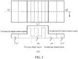
- FIG. 3 is a structure diagram illustrating the silicon-based modulator according to another embodiment of the present invention.
- the silicon-based modulator includes: a first heavily doped contact region, a second heavily doped contact region, and a modulation arm working region including a first type doped region and a second type doped region. And the first heavily doped contact region and the second heavily doped contact region are located at the left and right sides of the modulation arm working region, respectively.
- the first heavily doped contact region is connected with the first type doped region.
- a PN junction is formed in a contact region between the first type doped region and the second type doped region.
- the silicon-based modulator when the silicon-based modulator is looked down, there are multiple strip-shaped first type doped regions and multiple strip-shaped second type doped regions in the modulation arm working region.
- the strip-shaped first type doped regions and the strip-shaped second type doped regions are distributed in an alternating continuous manner. All the strip-shaped first type doped regions run through each other. All the strip-shaped second type doped regions run through each other.
- An intersection line of PN junctions between the first type doped regions and the second type doped regions of the modulation arm working region and a first plane is presented as a rectangular wave-like broken line.
- the first plane is formed by sectioning along an A1-A2 line when the silicon-based modulator is looked down.
- the strip-shaped first type doped regions and the strip-shaped second type doped regions are all parallel to a contact plane between the first heavily doped contact region or the second heavily doped contact region and the modulation arm working region.
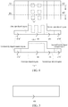
- FIG. 4 is a structure diagram illustrating the silicon-based modulator according to another embodiment of the present invention.
- the silicon-based modulator includes: a first heavily doped contact region, a second heavily doped contact region, and a modulation arm working region including a first type doped region and a second type doped region. And the first heavily doped contact region and the second heavily doped contact region are located at the left and right sides of the modulation arm working region, respectively.
- the first heavily doped contact region is connected with the first type doped region.
- a PN junction is formed in a contact region between the first type doped region and the second type doped region.
- the second type doped regions in the modulation arm working region are distributed in the first type doped regions in a dot matrix manner.
- Some intersection lines of PN junctions between the first type doped regions and the second type doped regions of the modulation arm working region and a first plane are presented as rectangular wave-like broken lines, and some intersection lines are presented as L-like broken lines.
- the first type doped regions are connected in an integral run-through manner, and the second type doped regions are connected in an integral run-through manner.
- the first plane is a longitudinal section of the silicon-based modulator.
- the first plane corresponding to the intersection lines presented as the rectangular wave-like broken lines and the first plane corresponding to the intersection lines presented as the L-like broken lines are two different planes.
- the intersection lines presented as the rectangular wave-like broken lines are located on a section formed by sectioning along an A1-A2 line.
- the intersection lines presented as the L-like broken lines are located on a section formed by sectioning along a B1-B2 line.
- the method includes the steps as follows.
- step 1 a first type (n or p type) doped SOI substrate is provided, and a substrate of which the doping concentration is in a range from 1E17cm-3 to 1E19cm-3 is directly used, or the doping concentration is adjusted to be within this range by using an ion injection manner, as shown in FIG. 5 .
- step 2 an optical waveguide is fabricated by utilizing a photo-etching process, to obtain a structure as shown in FIG. 6 .
- step 3 contact regions at two sides of the optical waveguide are set by utilizing the photo-etching process, and then corresponding ions are injected by utilizing an ion injection manner respectively, to implement a heavily doped region of which the doping concentration is in a range from 1E19cm-3 to 1E21cm-3, as shown in FIG. 7 .
- step 4 a second type (p or n type) ion doped region is set by utilizing the photo-etching process.
- step 5 second type ions are vertically and longitudinally injected, and the injected ions are annealed and activated, herein the annealed second doping concentration range is 1E17cm-3 to 1E19cm-3, and the structure is as shown in FIG. 8 .
- an embodiment of the present invention further provides a method for fabricating a silicon-based modulator.
- the method includes the steps as follows.
- a first type doped substrate is formed, and an optical waveguide is fabricated from the first type doped substrate by utilizing an etching process.
- Contact regions at two sides of the optical waveguide are formed by utilizing the etching process, and then first type ions or second type ions with a set concentration are injected into the two contact regions respectively by utilizing an ion injection manner, to form a first heavily doped contact region and a second heavily doped contact region.
- the method further includes the steps as follows.
- a second type doped region is formed by directly utilizing the ion injection manner, to obtain a modulation arm working region. Or, a pattern of a second type doped region on a horizontal plane is set by utilizing the etching process, and second type ions with a set concentration are then injected by utilizing the ion injection manner, and the second type doped region is formed by annealing, to obtain a modulation arm working region.
- an area of a contact region formed between a first type doped region and the second type doped region in the modulation arm working region is greater than an area of the smallest contact region between the first type doped region and the second type doped region.
- the first type doped region and the second type doped region form a P region and an N region in a PN junction by doping.
- the doped regions in this case are of a non-special shape, so the substrate of a first type doped region may be formed by means of an ion diffusion process or an ion injection process.
- the remaining first type doped region substrate part is the first type doped region.
- the operation that a second type doped region is formed by directly utilizing the ion injection manner to obtain a modulation arm working region includes the step as follows.
- Second type ions are injected into the optical waveguide for one or more times within a set angle range, and then the injected second type ions are annealed and activated to form a second type doped region with a set ion concentration, to obtain a modulation arm working region.
- the set angle range is an angle of 15 to 75 degrees relative to a vertical direction, and parallelism to a horizontal connecting line between the first heavily doped contact region and the second heavily doped contact region.
- the operation that a second type doped region is formed by utilizing the etching process and the ion injection manner to obtain a modulation arm working region includes the steps as follows.
- a pattern of the second type doped region on a horizontal plane is set by utilizing the etching process, and the pattern is multiple strips spaced from each other.
- Second type ions are vertically and longitudinally injected into a pattern region corresponding to the second type doped region, and a photosensitive material on the first type doped region is removed.
- the second type ions are injected into the optical waveguide for one or more times within a set angle range.
- the injected second type ions are annealed and activated to form a second type doped region with a set ion concentration, to obtain a modulation arm working region.
- the set angle range is an angle of 15 to 75 degrees relative to a vertical direction, and parallelism to a horizontal connecting line between the first heavily doped contact region and the second heavily doped contact region.
- the operation that a second type doped region is formed by utilizing the etching process and the ion injection manner to obtain a modulation arm working region includes the steps as follows.
- a pattern of a second type doped region on a horizontal plane is set by utilizing the etching process, and the pattern is a dot matrix shape.
- Second type ions are vertically and longitudinally injected into a pattern region corresponding to the second type doped region, and a photosensitive material on the first type doped region is removed.
- the second type ions are injected into the optical waveguide for one or more times within a set angle range.
- the injected second type ions are annealed and activated to form a second type doped region with a set ion concentration, to obtain a modulation arm working region.
- the set angle range is an angle of 15 to 75 degrees relative to a vertical direction, and parallelism to a horizontal connecting line between the first heavily doped contact region and the second heavily doped contact region.
- the structure of the silicon-based modulator in the present embodiment is as shown in FIG. 2 .
- a fabricating method thereof is as follows.
- Step 1 to step 3 are completely identical to those of the above traditional method for fabricating the silicon-based modulator, and will not be elaborated herein.
- an ion injection angle (presenting 15 to 75 degrees relative to a vertical direction, and parallel to the A1-A2 line in FIG. 2 ) is adjusted, and second type ions are injected for one or more times (it can be ensured that the second type ions are not injected into a first type doped region at the left, namely an n/p region by adjusting the injection angle or increasing the area of a heavily doped contact region at the left namely an n+/p+ region), and the depth (the depth is higher as the energy is higher) and concentration (the concentration is higher as the dosage is higher) of a PN junction are controlled by adjusting the injection energy and dosage of the second type ions, to make a PN junction region close to a middle position of a modulation arm working region to the greatest extent finally. And then the injected ions are annealed and activated, and the doping concentration range of the annealed second type ions is 1E17cm-3 to 1E19cm-3, as shown in FIG. 9 .
- the embodiments of the present invention have the advantages as follows.
- the structure of the silicon-based modulator of the present embodiment is as shown in FIG. 3 .
- the fabricating method thereof is as follows.
- Step 1 to step 3 are completely identical to those of the above traditional method for fabricating the silicon-based modulator, and will not be elaborated herein.
- step 4 a pattern of a strip-shaped second type doped region on a horizontal plane is set by utilizing a photo-etching technology.
- the pattern of the second type doped region on the horizontal plane is set, it is required to coat a photosensitive material such as photoresist, and after the pattern of the second type doped region on the horizontal plane is formed, the photoresist on a first type doped region is not removed yet to prevent second type ions from being injected into the first type doped region when the second type ions are injected subsequently for the first time.
- a photosensitive material such as photoresist
- step 5 during first-time injection of the second type ions, the second type ions are vertically and longitudinally injected to obtain a single/multi-junction strip-shaped injection structure as shown in FIG. 10 , and then the photoresist on the first type doped region is removed.
- an ion injection angle (presenting 15 to 75 degrees relative to a vertical direction, and parallel to the A1-A2 line in FIG. 3 ) is adjusted, and the second type ions are injected for one or more times to communicate multiple strip-shaped structures.
- the depth and concentration of a PN junction are controlled by adjusting the energy and dosage of the ion injection.
- the injection depth is close to a surface position of the modulation arm working region to the greatest extent.
- the injected second type ions are annealed and activated, and the doping concentration range of the annealed second type ions is 1E17cm-3 to 1E19cm-3, to obtain the structure as shown in FIG. 11 .
- the position of the PN junction in an optical waveguide is adjusted to realize modulation efficiency as high as possible.
- the embodiments of the present invention have the advantages as follows.
- a structure of the silicon-based modulator of the present embodiment is as shown in FIG. 4 .
- the fabricating method thereof is as follows.
- Step 1 to step 3 are completely identical to those of the above traditional method for fabricating the silicon-based modulator, and will not be elaborated herein.
- step 4 a pattern of a dot matrix shaped second type doped region on a horizontal plane is set by utilizing a photo-etching technology.
- the pattern of the second type doped region on the horizontal plane is set, it is required to coat a photosensitive material such as photoresist, and after the pattern of the second type doped region on the horizontal plane is formed, the photoresist on a first type doped region is not removed yet to prevent second type ions from being injected into the first type doped region when the second type ions are injected subsequently for the first time.
- a photosensitive material such as photoresist
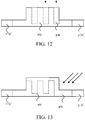
- step 5 during first-time injection of the second type ions, the second type ions are vertically and longitudinally injected to implement a multi-column injection structure, and then the photoresist on the first type doped region is removed, to obtain a structure as shown in FIG. 12 (sectional view of a silicon-based modulator along an A1-A2 line in FIG. 4 ).
- an ion injection angle (presenting 15 to 75 degrees relative to a vertical direction, and parallel to the A1-A2 line in FIG. 3 ) is adjusted, and the second type ions are injected for one or more times to communicate multiple columnar structures.
- the depth and concentration of a PN junction are controlled by adjusting the energy and dosage of ion injection.
- the injection depth is close to a surface position of a modulation arm working region to the greatest extent.
- the injected second type ions are annealed and activated, and the doping concentration range of the annealed second type ions is 1E17cm-3 to 1E19cm-3, to obtain a structure as shown in FIG. 13 .
- the position of the PN junction in an optical waveguide is adjusted to realize modulation efficiency as high as possible.
- the embodiments of the present invention have the advantages as follows.
- the embodiments of the present invention may be provided as a method, a system or a computer program product.
- forms of hardware embodiments, software embodiments or embodiments integrating software and hardware may be adopted in the present invention.
- a form of the computer program product implemented on one or more computer available storage media including, but are not limited to, a disk memory, an optical memory and the like
- computer available program codes may be adopted in the present invention.
- each flow and/or block in the flowcharts and/or the block diagrams and a combination of the flows and/or the blocks in the flowcharts and/or the block diagrams may be implemented by computer program instructions.
- These computer program instructions may be provided for a general computer, a dedicated computer, an embedded processor or processors of other programmable data processing devices to generate a machine, such that an apparatus for implementing functions designated in one or more flows of the flowcharts and/or one or more blocks of the block diagrams is generated via instructions executed by the computers or the processors of the other programmable data processing devices.
- These computer program instructions may also be stored in a computer readable memory capable of guiding the computers or the other programmable data processing devices to work in a specific mode, such that a manufactured product including an instruction apparatus is generated via the instructions stored in the computer readable memory, and the instruction apparatus implements the functions designated in one or more flows of the flowcharts and/or one or more blocks of the block diagrams.
- the embodiments of the present invention provide a silicon-based modulator and a method for fabricating the silicon-based modulator.
- the silicon-based modulator includes: a first heavily doped contact region, a second heavily doped contact region, and a modulation arm working region including a first type doped region and a second type doped region.
- the first heavily doped contact region and the second heavily doped contact region are located at the left and right sides of the modulation arm working region, respectively.
- the first heavily doped contact region is connected with the first type doped region.
- a PN junction is formed in a contact region between the first type doped region and the second type doped region.
- An area of the contact region formed between the first type doped region and the second type doped region in the modulation arm working region is greater than an area of a smallest contact region between the first type doped region and the second type doped region.
Landscapes
- Physics & Mathematics (AREA)
- Nonlinear Science (AREA)
- General Physics & Mathematics (AREA)
- Optics & Photonics (AREA)
- Optical Modulation, Optical Deflection, Nonlinear Optics, Optical Demodulation, Optical Logic Elements (AREA)
Applications Claiming Priority (2)
| Application Number | Priority Date | Filing Date | Title |
|---|---|---|---|
| CN201510175428.4A CN106154680A (zh) | 2015-04-14 | 2015-04-14 | 一种硅基调制器及其制备方法 |
| PCT/CN2016/079060 WO2016165608A1 (zh) | 2015-04-14 | 2016-04-12 | 一种硅基调制器及其制备方法 |
Publications (3)
| Publication Number | Publication Date |
|---|---|
| EP3264166A1 true EP3264166A1 (de) | 2018-01-03 |
| EP3264166A4 EP3264166A4 (de) | 2018-03-14 |
| EP3264166B1 EP3264166B1 (de) | 2020-04-29 |
Family
ID=57125726
Family Applications (1)
| Application Number | Title | Priority Date | Filing Date |
|---|---|---|---|
| EP16779583.0A Active EP3264166B1 (de) | 2015-04-14 | 2016-04-12 | Siliciumbasierter modulator und verfahren zur herstellung davon |
Country Status (3)
| Country | Link |
|---|---|
| EP (1) | EP3264166B1 (de) |
| CN (1) | CN106154680A (de) |
| WO (1) | WO2016165608A1 (de) |
Cited By (3)
| Publication number | Priority date | Publication date | Assignee | Title |
|---|---|---|---|---|
| WO2020084080A1 (en) * | 2018-10-24 | 2020-04-30 | Rockley Photonics Limited | Pn-junction phase modulator in a large silicon waveguide platform |
| WO2021048018A1 (en) * | 2019-09-09 | 2021-03-18 | Rockley Photonics Limited | Optoelectronic device and method of manufacturing an optoelectronic device |
| US11454857B2 (en) * | 2018-08-17 | 2022-09-27 | Taiwan Semiconductor Manufacturing Co., Ltd. | Folded waveguide phase shifters |
Families Citing this family (4)
| Publication number | Priority date | Publication date | Assignee | Title |
|---|---|---|---|---|
| CN111999917B (zh) * | 2020-08-18 | 2022-03-25 | 华中科技大学 | 一种电光移相器掺杂结构、制备方法及电光调制器 |
| US12353069B2 (en) * | 2021-05-06 | 2025-07-08 | Taiwan Semiconductor Manufacturing Company, Ltd. | Waveguide having doped pillar structures to improve modulator efficiency |
| US12429718B1 (en) * | 2022-06-23 | 2025-09-30 | Marvell Asia Pte Ltd | Ultra-high bandwidth multi-junction silicon optical modulator |
| US12386211B2 (en) * | 2022-10-20 | 2025-08-12 | Nokia Solutions And Networks Oy | Silicon optical phase shifter with a series of P—N junctions |
Family Cites Families (7)
| Publication number | Priority date | Publication date | Assignee | Title |
|---|---|---|---|---|
| US7116853B2 (en) * | 2003-08-15 | 2006-10-03 | Luxtera, Inc. | PN diode optical modulators fabricated in rib waveguides |
| US20110176762A1 (en) * | 2008-11-13 | 2011-07-21 | Junichi Fujikata | Optical modulator and optical modulator fabrication method |
| US8548281B2 (en) * | 2009-09-08 | 2013-10-01 | Electronics And Telecommunications Research Institute | Electro-optic modulating device |
| CN202563200U (zh) * | 2012-01-10 | 2012-11-28 | 东南大学 | 一种马赫-曾德尔硅光调制器 |
| CN103226252B (zh) * | 2013-05-06 | 2016-05-18 | 中国科学院半导体研究所 | 一种提高耗尽型硅基电光调制器调制效率的掺杂结构 |
| WO2014185951A1 (en) * | 2013-05-14 | 2014-11-20 | Silicon Lightwave Services | Ultra-responsive phase shifters for depletion mode silicon modulators |
| CN204155033U (zh) * | 2014-11-06 | 2015-02-11 | 江苏尚飞光电科技有限公司 | 硅基光调制器 |
-
2015
- 2015-04-14 CN CN201510175428.4A patent/CN106154680A/zh active Pending
-
2016
- 2016-04-12 WO PCT/CN2016/079060 patent/WO2016165608A1/zh not_active Ceased
- 2016-04-12 EP EP16779583.0A patent/EP3264166B1/de active Active
Cited By (9)
| Publication number | Priority date | Publication date | Assignee | Title |
|---|---|---|---|---|
| US11454857B2 (en) * | 2018-08-17 | 2022-09-27 | Taiwan Semiconductor Manufacturing Co., Ltd. | Folded waveguide phase shifters |
| WO2020084080A1 (en) * | 2018-10-24 | 2020-04-30 | Rockley Photonics Limited | Pn-junction phase modulator in a large silicon waveguide platform |
| US11054674B2 (en) | 2018-10-24 | 2021-07-06 | Rockley Photonics Limited | PN-junction phase modulator in a large silicon waveguide platform |
| GB2593354A (en) * | 2018-10-24 | 2021-09-22 | Rockley Photonics Ltd | PN-junction phase modulator in a large silicon waveguide platform |
| GB2593354B (en) * | 2018-10-24 | 2023-02-08 | Rockley Photonics Ltd | PN-junction phase modulator in a large silicon waveguide platform |
| WO2021048018A1 (en) * | 2019-09-09 | 2021-03-18 | Rockley Photonics Limited | Optoelectronic device and method of manufacturing an optoelectronic device |
| US20220342240A1 (en) * | 2019-09-09 | 2022-10-27 | Rockley Photonics Limited | Optoelectronic device and method of manufacturing an optoelectronic device |
| GB2586881B (en) * | 2019-09-09 | 2023-08-16 | Rockley Photonics Ltd | Optoelectronic device and method of manufacturing an optoelectronic device |
| US12292624B2 (en) * | 2019-09-09 | 2025-05-06 | Rockley Photonics Limited | Optoelectronic device and method of manufacturing an optoelectronic device |
Also Published As
| Publication number | Publication date |
|---|---|
| EP3264166A4 (de) | 2018-03-14 |
| EP3264166B1 (de) | 2020-04-29 |
| CN106154680A (zh) | 2016-11-23 |
| WO2016165608A1 (zh) | 2016-10-20 |
Similar Documents
| Publication | Publication Date | Title |
|---|---|---|
| EP3264166B1 (de) | Siliciumbasierter modulator und verfahren zur herstellung davon | |
| CN103226252B (zh) | 一种提高耗尽型硅基电光调制器调制效率的掺杂结构 | |
| US10658459B2 (en) | Nanosheet transistor with robust source/drain isolation from substrate | |
| CN103811499B (zh) | 薄膜晶体管阵列面板及其制造方法 | |
| CN104124157B (zh) | 半导体装置及其制造方法 | |
| CN104183542A (zh) | 电熔丝结构及其形成方法、半导体器件及其形成方法 | |
| US9923040B2 (en) | Array substrate and display device | |
| WO2016150263A1 (zh) | 一种pn结 | |
| EP3239771A1 (de) | Flüssigkristallanzeigetafel, herstellungsverfahren und anzeigevorrichtung dafür | |
| SG11201806226WA (en) | Field effect transistor, method for manufacturing same, display element, display device, and system | |
| TW201539715A (zh) | 包括凹入式存取裝置之半導體裝置及其形成方法 | |
| CN108447896B (zh) | 碳化硅功率器件终端结构的制造方法 | |
| CN104932159A (zh) | 显示基板及其制造方法、驱动方法和显示装置 | |
| US10042211B2 (en) | Liquid crystal display panel, array substrate and manufacturing method thereof | |
| US10134765B2 (en) | Oxide semiconductor TFT array substrate and method for manufacturing the same | |
| US10991724B2 (en) | CMOS transistor and method for fabricating the same, display panel and display device | |
| US20160041316A1 (en) | Display substrate and manufacturing method thereof, and display apparatus | |
| DE102015117230A1 (de) | Verfahren zum Bilden einer Halbleitervorrichtungsstruktur | |
| CN106298479A (zh) | 一种功率器件的结终端扩展结构及其制造方法 | |
| CN104465360A (zh) | 晶圆及其刻蚀方法 | |
| CN106129810B (zh) | 半导体装置的制造方法、半导体装置 | |
| CN104599972B (zh) | 一种半导体器件及其形成方法 | |
| CN109643686B (zh) | 具有侧面扩散的沟槽插塞的半导体器件 | |
| CN103633149A (zh) | 恒流二极管及其制造方法 | |
| CN106298802B (zh) | 一种ltps阵列基板及制造方法、显示面板 |
Legal Events
| Date | Code | Title | Description |
|---|---|---|---|
| STAA | Information on the status of an ep patent application or granted ep patent |
Free format text: STATUS: THE INTERNATIONAL PUBLICATION HAS BEEN MADE |
|
| PUAI | Public reference made under article 153(3) epc to a published international application that has entered the european phase |
Free format text: ORIGINAL CODE: 0009012 |
|
| STAA | Information on the status of an ep patent application or granted ep patent |
Free format text: STATUS: REQUEST FOR EXAMINATION WAS MADE |
|
| 17P | Request for examination filed |
Effective date: 20170929 |
|
| AK | Designated contracting states |
Kind code of ref document: A1 Designated state(s): AL AT BE BG CH CY CZ DE DK EE ES FI FR GB GR HR HU IE IS IT LI LT LU LV MC MK MT NL NO PL PT RO RS SE SI SK SM TR |
|
| AX | Request for extension of the european patent |
Extension state: BA ME |
|
| A4 | Supplementary search report drawn up and despatched |
Effective date: 20180212 |
|
| RIC1 | Information provided on ipc code assigned before grant |
Ipc: H01L 21/02 20060101ALI20180206BHEP Ipc: G02F 1/225 20060101ALI20180206BHEP Ipc: G02F 1/025 20060101AFI20180206BHEP |
|
| DAV | Request for validation of the european patent (deleted) | ||
| DAX | Request for extension of the european patent (deleted) | ||
| GRAP | Despatch of communication of intention to grant a patent |
Free format text: ORIGINAL CODE: EPIDOSNIGR1 |
|
| STAA | Information on the status of an ep patent application or granted ep patent |
Free format text: STATUS: GRANT OF PATENT IS INTENDED |
|
| RIC1 | Information provided on ipc code assigned before grant |
Ipc: H01L 21/02 20060101ALI20191211BHEP Ipc: G02F 1/225 20060101ALI20191211BHEP Ipc: G02F 1/025 20060101AFI20191211BHEP |
|
| INTG | Intention to grant announced |
Effective date: 20200109 |
|
| GRAS | Grant fee paid |
Free format text: ORIGINAL CODE: EPIDOSNIGR3 |
|
| GRAA | (expected) grant |
Free format text: ORIGINAL CODE: 0009210 |
|
| STAA | Information on the status of an ep patent application or granted ep patent |
Free format text: STATUS: THE PATENT HAS BEEN GRANTED |
|
| AK | Designated contracting states |
Kind code of ref document: B1 Designated state(s): AL AT BE BG CH CY CZ DE DK EE ES FI FR GB GR HR HU IE IS IT LI LT LU LV MC MK MT NL NO PL PT RO RS SE SI SK SM TR |
|
| REG | Reference to a national code |
Ref country code: GB Ref legal event code: FG4D |
|
| REG | Reference to a national code |
Ref country code: CH Ref legal event code: EP |
|
| REG | Reference to a national code |
Ref country code: AT Ref legal event code: REF Ref document number: 1264193 Country of ref document: AT Kind code of ref document: T Effective date: 20200515 |
|
| REG | Reference to a national code |
Ref country code: DE Ref legal event code: R096 Ref document number: 602016035207 Country of ref document: DE |
|
| REG | Reference to a national code |
Ref country code: IE Ref legal event code: FG4D |
|
| REG | Reference to a national code |
Ref country code: NL Ref legal event code: MP Effective date: 20200429 |
|
| REG | Reference to a national code |
Ref country code: LT Ref legal event code: MG4D |
|
| PG25 | Lapsed in a contracting state [announced via postgrant information from national office to epo] |
Ref country code: FI Free format text: LAPSE BECAUSE OF FAILURE TO SUBMIT A TRANSLATION OF THE DESCRIPTION OR TO PAY THE FEE WITHIN THE PRESCRIBED TIME-LIMIT Effective date: 20200429 Ref country code: LT Free format text: LAPSE BECAUSE OF FAILURE TO SUBMIT A TRANSLATION OF THE DESCRIPTION OR TO PAY THE FEE WITHIN THE PRESCRIBED TIME-LIMIT Effective date: 20200429 Ref country code: PT Free format text: LAPSE BECAUSE OF FAILURE TO SUBMIT A TRANSLATION OF THE DESCRIPTION OR TO PAY THE FEE WITHIN THE PRESCRIBED TIME-LIMIT Effective date: 20200831 Ref country code: NO Free format text: LAPSE BECAUSE OF FAILURE TO SUBMIT A TRANSLATION OF THE DESCRIPTION OR TO PAY THE FEE WITHIN THE PRESCRIBED TIME-LIMIT Effective date: 20200729 Ref country code: IS Free format text: LAPSE BECAUSE OF FAILURE TO SUBMIT A TRANSLATION OF THE DESCRIPTION OR TO PAY THE FEE WITHIN THE PRESCRIBED TIME-LIMIT Effective date: 20200829 Ref country code: SE Free format text: LAPSE BECAUSE OF FAILURE TO SUBMIT A TRANSLATION OF THE DESCRIPTION OR TO PAY THE FEE WITHIN THE PRESCRIBED TIME-LIMIT Effective date: 20200429 Ref country code: GR Free format text: LAPSE BECAUSE OF FAILURE TO SUBMIT A TRANSLATION OF THE DESCRIPTION OR TO PAY THE FEE WITHIN THE PRESCRIBED TIME-LIMIT Effective date: 20200730 |
|
| REG | Reference to a national code |
Ref country code: AT Ref legal event code: MK05 Ref document number: 1264193 Country of ref document: AT Kind code of ref document: T Effective date: 20200429 |
|
| PG25 | Lapsed in a contracting state [announced via postgrant information from national office to epo] |
Ref country code: RS Free format text: LAPSE BECAUSE OF FAILURE TO SUBMIT A TRANSLATION OF THE DESCRIPTION OR TO PAY THE FEE WITHIN THE PRESCRIBED TIME-LIMIT Effective date: 20200429 Ref country code: HR Free format text: LAPSE BECAUSE OF FAILURE TO SUBMIT A TRANSLATION OF THE DESCRIPTION OR TO PAY THE FEE WITHIN THE PRESCRIBED TIME-LIMIT Effective date: 20200429 Ref country code: BG Free format text: LAPSE BECAUSE OF FAILURE TO SUBMIT A TRANSLATION OF THE DESCRIPTION OR TO PAY THE FEE WITHIN THE PRESCRIBED TIME-LIMIT Effective date: 20200729 Ref country code: LV Free format text: LAPSE BECAUSE OF FAILURE TO SUBMIT A TRANSLATION OF THE DESCRIPTION OR TO PAY THE FEE WITHIN THE PRESCRIBED TIME-LIMIT Effective date: 20200429 |
|
| PG25 | Lapsed in a contracting state [announced via postgrant information from national office to epo] |
Ref country code: NL Free format text: LAPSE BECAUSE OF FAILURE TO SUBMIT A TRANSLATION OF THE DESCRIPTION OR TO PAY THE FEE WITHIN THE PRESCRIBED TIME-LIMIT Effective date: 20200429 Ref country code: AL Free format text: LAPSE BECAUSE OF FAILURE TO SUBMIT A TRANSLATION OF THE DESCRIPTION OR TO PAY THE FEE WITHIN THE PRESCRIBED TIME-LIMIT Effective date: 20200429 |
|
| PG25 | Lapsed in a contracting state [announced via postgrant information from national office to epo] |
Ref country code: IT Free format text: LAPSE BECAUSE OF FAILURE TO SUBMIT A TRANSLATION OF THE DESCRIPTION OR TO PAY THE FEE WITHIN THE PRESCRIBED TIME-LIMIT Effective date: 20200429 Ref country code: DK Free format text: LAPSE BECAUSE OF FAILURE TO SUBMIT A TRANSLATION OF THE DESCRIPTION OR TO PAY THE FEE WITHIN THE PRESCRIBED TIME-LIMIT Effective date: 20200429 Ref country code: SM Free format text: LAPSE BECAUSE OF FAILURE TO SUBMIT A TRANSLATION OF THE DESCRIPTION OR TO PAY THE FEE WITHIN THE PRESCRIBED TIME-LIMIT Effective date: 20200429 Ref country code: EE Free format text: LAPSE BECAUSE OF FAILURE TO SUBMIT A TRANSLATION OF THE DESCRIPTION OR TO PAY THE FEE WITHIN THE PRESCRIBED TIME-LIMIT Effective date: 20200429 Ref country code: AT Free format text: LAPSE BECAUSE OF FAILURE TO SUBMIT A TRANSLATION OF THE DESCRIPTION OR TO PAY THE FEE WITHIN THE PRESCRIBED TIME-LIMIT Effective date: 20200429 Ref country code: RO Free format text: LAPSE BECAUSE OF FAILURE TO SUBMIT A TRANSLATION OF THE DESCRIPTION OR TO PAY THE FEE WITHIN THE PRESCRIBED TIME-LIMIT Effective date: 20200429 Ref country code: ES Free format text: LAPSE BECAUSE OF FAILURE TO SUBMIT A TRANSLATION OF THE DESCRIPTION OR TO PAY THE FEE WITHIN THE PRESCRIBED TIME-LIMIT Effective date: 20200429 Ref country code: CZ Free format text: LAPSE BECAUSE OF FAILURE TO SUBMIT A TRANSLATION OF THE DESCRIPTION OR TO PAY THE FEE WITHIN THE PRESCRIBED TIME-LIMIT Effective date: 20200429 |
|
| REG | Reference to a national code |
Ref country code: DE Ref legal event code: R097 Ref document number: 602016035207 Country of ref document: DE |
|
| PG25 | Lapsed in a contracting state [announced via postgrant information from national office to epo] |
Ref country code: PL Free format text: LAPSE BECAUSE OF FAILURE TO SUBMIT A TRANSLATION OF THE DESCRIPTION OR TO PAY THE FEE WITHIN THE PRESCRIBED TIME-LIMIT Effective date: 20200429 Ref country code: SK Free format text: LAPSE BECAUSE OF FAILURE TO SUBMIT A TRANSLATION OF THE DESCRIPTION OR TO PAY THE FEE WITHIN THE PRESCRIBED TIME-LIMIT Effective date: 20200429 |
|
| PLBE | No opposition filed within time limit |
Free format text: ORIGINAL CODE: 0009261 |
|
| STAA | Information on the status of an ep patent application or granted ep patent |
Free format text: STATUS: NO OPPOSITION FILED WITHIN TIME LIMIT |
|
| 26N | No opposition filed |
Effective date: 20210201 |
|
| PG25 | Lapsed in a contracting state [announced via postgrant information from national office to epo] |
Ref country code: SI Free format text: LAPSE BECAUSE OF FAILURE TO SUBMIT A TRANSLATION OF THE DESCRIPTION OR TO PAY THE FEE WITHIN THE PRESCRIBED TIME-LIMIT Effective date: 20200429 |
|
| PG25 | Lapsed in a contracting state [announced via postgrant information from national office to epo] |
Ref country code: MC Free format text: LAPSE BECAUSE OF FAILURE TO SUBMIT A TRANSLATION OF THE DESCRIPTION OR TO PAY THE FEE WITHIN THE PRESCRIBED TIME-LIMIT Effective date: 20200429 |
|
| PG25 | Lapsed in a contracting state [announced via postgrant information from national office to epo] |
Ref country code: LU Free format text: LAPSE BECAUSE OF NON-PAYMENT OF DUE FEES Effective date: 20210412 |
|
| REG | Reference to a national code |
Ref country code: BE Ref legal event code: MM Effective date: 20210430 |
|
| PG25 | Lapsed in a contracting state [announced via postgrant information from national office to epo] |
Ref country code: CH Free format text: LAPSE BECAUSE OF NON-PAYMENT OF DUE FEES Effective date: 20210430 Ref country code: LI Free format text: LAPSE BECAUSE OF NON-PAYMENT OF DUE FEES Effective date: 20210430 |
|
| PG25 | Lapsed in a contracting state [announced via postgrant information from national office to epo] |
Ref country code: IE Free format text: LAPSE BECAUSE OF NON-PAYMENT OF DUE FEES Effective date: 20210412 |
|
| PG25 | Lapsed in a contracting state [announced via postgrant information from national office to epo] |
Ref country code: BE Free format text: LAPSE BECAUSE OF NON-PAYMENT OF DUE FEES Effective date: 20210430 |
|
| PG25 | Lapsed in a contracting state [announced via postgrant information from national office to epo] |
Ref country code: HU Free format text: LAPSE BECAUSE OF FAILURE TO SUBMIT A TRANSLATION OF THE DESCRIPTION OR TO PAY THE FEE WITHIN THE PRESCRIBED TIME-LIMIT; INVALID AB INITIO Effective date: 20160412 |
|
| PG25 | Lapsed in a contracting state [announced via postgrant information from national office to epo] |
Ref country code: CY Free format text: LAPSE BECAUSE OF FAILURE TO SUBMIT A TRANSLATION OF THE DESCRIPTION OR TO PAY THE FEE WITHIN THE PRESCRIBED TIME-LIMIT Effective date: 20200429 |
|
| PG25 | Lapsed in a contracting state [announced via postgrant information from national office to epo] |
Ref country code: MK Free format text: LAPSE BECAUSE OF FAILURE TO SUBMIT A TRANSLATION OF THE DESCRIPTION OR TO PAY THE FEE WITHIN THE PRESCRIBED TIME-LIMIT Effective date: 20200429 |
|
| PG25 | Lapsed in a contracting state [announced via postgrant information from national office to epo] |
Ref country code: MT Free format text: LAPSE BECAUSE OF FAILURE TO SUBMIT A TRANSLATION OF THE DESCRIPTION OR TO PAY THE FEE WITHIN THE PRESCRIBED TIME-LIMIT Effective date: 20200429 |
|
| PGFP | Annual fee paid to national office [announced via postgrant information from national office to epo] |
Ref country code: DE Payment date: 20250305 Year of fee payment: 10 |
|
| PG25 | Lapsed in a contracting state [announced via postgrant information from national office to epo] |
Ref country code: TR Free format text: LAPSE BECAUSE OF FAILURE TO SUBMIT A TRANSLATION OF THE DESCRIPTION OR TO PAY THE FEE WITHIN THE PRESCRIBED TIME-LIMIT Effective date: 20200429 |
|
| PGFP | Annual fee paid to national office [announced via postgrant information from national office to epo] |
Ref country code: GB Payment date: 20260312 Year of fee payment: 11 |
|
| PGFP | Annual fee paid to national office [announced via postgrant information from national office to epo] |
Ref country code: FR Payment date: 20260309 Year of fee payment: 11 |