EP3260572A1 - Tantalum sputtering target, and production method therefor - Google Patents
Tantalum sputtering target, and production method therefor Download PDFInfo
- Publication number
- EP3260572A1 EP3260572A1 EP16799865.7A EP16799865A EP3260572A1 EP 3260572 A1 EP3260572 A1 EP 3260572A1 EP 16799865 A EP16799865 A EP 16799865A EP 3260572 A1 EP3260572 A1 EP 3260572A1
- Authority
- EP
- European Patent Office
- Prior art keywords
- target
- sputtering
- tantalum
- rolling
- plane
- Prior art date
- Legal status (The legal status is an assumption and is not a legal conclusion. Google has not performed a legal analysis and makes no representation as to the accuracy of the status listed.)
- Granted
Links
Images


Classifications
-
- C—CHEMISTRY; METALLURGY
- C23—COATING METALLIC MATERIAL; COATING MATERIAL WITH METALLIC MATERIAL; CHEMICAL SURFACE TREATMENT; DIFFUSION TREATMENT OF METALLIC MATERIAL; COATING BY VACUUM EVAPORATION, BY SPUTTERING, BY ION IMPLANTATION OR BY CHEMICAL VAPOUR DEPOSITION, IN GENERAL; INHIBITING CORROSION OF METALLIC MATERIAL OR INCRUSTATION IN GENERAL
- C23C—COATING METALLIC MATERIAL; COATING MATERIAL WITH METALLIC MATERIAL; SURFACE TREATMENT OF METALLIC MATERIAL BY DIFFUSION INTO THE SURFACE, BY CHEMICAL CONVERSION OR SUBSTITUTION; COATING BY VACUUM EVAPORATION, BY SPUTTERING, BY ION IMPLANTATION OR BY CHEMICAL VAPOUR DEPOSITION, IN GENERAL
- C23C14/00—Coating by vacuum evaporation, by sputtering or by ion implantation of the coating forming material
- C23C14/22—Coating by vacuum evaporation, by sputtering or by ion implantation of the coating forming material characterised by the process of coating
- C23C14/34—Sputtering
- C23C14/3407—Cathode assembly for sputtering apparatus, e.g. Target
- C23C14/3414—Metallurgical or chemical aspects of target preparation, e.g. casting, powder metallurgy
-
- B—PERFORMING OPERATIONS; TRANSPORTING
- B21—MECHANICAL METAL-WORKING WITHOUT ESSENTIALLY REMOVING MATERIAL; PUNCHING METAL
- B21J—FORGING; HAMMERING; PRESSING METAL; RIVETING; FORGE FURNACES
- B21J1/00—Preparing metal stock or similar ancillary operations prior, during or post forging, e.g. heating or cooling
- B21J1/003—Selecting material
-
- C—CHEMISTRY; METALLURGY
- C22—METALLURGY; FERROUS OR NON-FERROUS ALLOYS; TREATMENT OF ALLOYS OR NON-FERROUS METALS
- C22C—ALLOYS
- C22C27/00—Alloys based on rhenium or a refractory metal not mentioned in groups C22C14/00 or C22C16/00
- C22C27/02—Alloys based on vanadium, niobium, or tantalum
-
- C—CHEMISTRY; METALLURGY
- C22—METALLURGY; FERROUS OR NON-FERROUS ALLOYS; TREATMENT OF ALLOYS OR NON-FERROUS METALS
- C22F—CHANGING THE PHYSICAL STRUCTURE OF NON-FERROUS METALS AND NON-FERROUS ALLOYS
- C22F1/00—Changing the physical structure of non-ferrous metals or alloys by heat treatment or by hot or cold working
-
- C—CHEMISTRY; METALLURGY
- C23—COATING METALLIC MATERIAL; COATING MATERIAL WITH METALLIC MATERIAL; CHEMICAL SURFACE TREATMENT; DIFFUSION TREATMENT OF METALLIC MATERIAL; COATING BY VACUUM EVAPORATION, BY SPUTTERING, BY ION IMPLANTATION OR BY CHEMICAL VAPOUR DEPOSITION, IN GENERAL; INHIBITING CORROSION OF METALLIC MATERIAL OR INCRUSTATION IN GENERAL
- C23C—COATING METALLIC MATERIAL; COATING MATERIAL WITH METALLIC MATERIAL; SURFACE TREATMENT OF METALLIC MATERIAL BY DIFFUSION INTO THE SURFACE, BY CHEMICAL CONVERSION OR SUBSTITUTION; COATING BY VACUUM EVAPORATION, BY SPUTTERING, BY ION IMPLANTATION OR BY CHEMICAL VAPOUR DEPOSITION, IN GENERAL
- C23C14/00—Coating by vacuum evaporation, by sputtering or by ion implantation of the coating forming material
- C23C14/22—Coating by vacuum evaporation, by sputtering or by ion implantation of the coating forming material characterised by the process of coating
- C23C14/34—Sputtering
-
- C—CHEMISTRY; METALLURGY
- C23—COATING METALLIC MATERIAL; COATING MATERIAL WITH METALLIC MATERIAL; CHEMICAL SURFACE TREATMENT; DIFFUSION TREATMENT OF METALLIC MATERIAL; COATING BY VACUUM EVAPORATION, BY SPUTTERING, BY ION IMPLANTATION OR BY CHEMICAL VAPOUR DEPOSITION, IN GENERAL; INHIBITING CORROSION OF METALLIC MATERIAL OR INCRUSTATION IN GENERAL
- C23C—COATING METALLIC MATERIAL; COATING MATERIAL WITH METALLIC MATERIAL; SURFACE TREATMENT OF METALLIC MATERIAL BY DIFFUSION INTO THE SURFACE, BY CHEMICAL CONVERSION OR SUBSTITUTION; COATING BY VACUUM EVAPORATION, BY SPUTTERING, BY ION IMPLANTATION OR BY CHEMICAL VAPOUR DEPOSITION, IN GENERAL
- C23C14/00—Coating by vacuum evaporation, by sputtering or by ion implantation of the coating forming material
- C23C14/22—Coating by vacuum evaporation, by sputtering or by ion implantation of the coating forming material characterised by the process of coating
- C23C14/34—Sputtering
- C23C14/3407—Cathode assembly for sputtering apparatus, e.g. Target
-
- B—PERFORMING OPERATIONS; TRANSPORTING
- B21—MECHANICAL METAL-WORKING WITHOUT ESSENTIALLY REMOVING MATERIAL; PUNCHING METAL
- B21J—FORGING; HAMMERING; PRESSING METAL; RIVETING; FORGE FURNACES
- B21J1/00—Preparing metal stock or similar ancillary operations prior, during or post forging, e.g. heating or cooling
- B21J1/02—Preliminary treatment of metal stock without particular shaping, e.g. salvaging segregated zones, forging or pressing in the rough
-
- C—CHEMISTRY; METALLURGY
- C22—METALLURGY; FERROUS OR NON-FERROUS ALLOYS; TREATMENT OF ALLOYS OR NON-FERROUS METALS
- C22F—CHANGING THE PHYSICAL STRUCTURE OF NON-FERROUS METALS AND NON-FERROUS ALLOYS
- C22F1/00—Changing the physical structure of non-ferrous metals or alloys by heat treatment or by hot or cold working
- C22F1/16—Changing the physical structure of non-ferrous metals or alloys by heat treatment or by hot or cold working of other metals or alloys based thereon
- C22F1/18—High-melting or refractory metals or alloys based thereon
Definitions
- the present invention relates to a tantalum sputtering target suitable for forming a barrier seed layer in a wiring of a semiconductor integrated circuit, and particularly the tantalum sputtering target that are capable of achieving thickness uniformity even under high-power sputtering conditions by increasing the straightness of the sputtered material and a method for producing the tantalum sputtering target.
- the sputtering method for forming films from metals, ceramics and other materials has been used in numerous fields such as electronics, corrosion resistant materials and ornaments, catalysts, as well as in the manufacture of cutting/polishing materials and abrasion resistant materials. While the sputtering method itself is a well-known method in the foregoing fields, a tantalum sputtering target suitable for forming films of complex shapes or forming circuits are more in demand especially in the electronics field.
- this tantalum target is manufactured by performing forging and annealing (i.e. heat treatment) to an ingot or a billet obtained by subjecting a tantalum raw material to electron beam melting and casting, and thereafter performing rolling and finish processing such as machining and polishing to the ingot or billet to obtain a target.
- forging and recrystallization annealing to the ingot or billet obtained via melting/casting will destroy the cast structure, and uniform and fine crystal grains are consequently obtained.
- Patent Documents 1 to 11 When performing sputtering, as the crystal grains of the target are finer and more uniform, more uniform deposition is enabled and a film with stable characteristics can be obtained. It is also effective to align the crystal orientation across the entire thickness direction of the target to improve the uniformity of deposition. Note that the following background art are known in relation to a tantalum sputtering target (Patent Documents 1 to 11).
- High-power sputtering using a magnetron sputtering device is being performed to increase the deposition rate of sputtering in recent years.
- high-power sputtering it is difficult to control the direction of the material sputtered from the target and to uniformly deposit a sputtered material on the wafer surface in a wiring of semiconductor integrated circuits which is constantly being refined.
- the issues are especially notable when embedding wiring holes having a large aspect ratio.
- An object of the present invention is to provide a tantalum sputtering target in which high-speed and uniform deposition is enabled under high-power sputtering conditions.
- sputter-deposition is performed using this kind of tantalum target, it is possible to form a thin film having superior film thickness uniformity and improve the productivity of the thin film formation process, even for fine wiring.
- the present inventors conducted research and found out that, when the structural orientation of a tantalum sputtering target is caused to be a predetermined state by devising the rolling method, the straightness of the sputtered material can be improved, the sputtered material can be uniformly deposited on the wafer surface, and even fine wiring holes having a high aspect ratio can be embedded effectively, and the throughput of deposition can be improved.
- the straightness of the sputtered material can be increased and the sputtered material can be uniformly deposited on the wafer surface even under high-power sputtering conditions by causing the structural orientation of a tantalum sputtering target to be a predetermined state, the film thickness uniformity and the throughput of deposition can be simultaneously improved even for fine wiring.
- Embodiments of the present invention provide a tantalum sputtering target that enables uniform deposition on wiring holes having a large aspect ratio.
- the sputtering target according to the embodiments of the present invention is characterized in that an area ratio of crystal grains of which a ⁇ 111 ⁇ plane is oriented in a direction normal to a rolling surface (ND) is 35% or more when the ND, which is a cross section orthogonal to a sputtering surface of a target, is observed by a method using Electron Backscatter Diffraction Patterns (abbreviated EBSP(s) hereinafter).
- EBSP(s) Electron Backscatter Diffraction Patterns
- the atomic close-packed direction is ⁇ 111>, and the relation of the sputtering surface and the close-packed direction is important in controlling the sputter direction of the sputtered material.
- the ⁇ 111 ⁇ plane is oriented in the direction normal to the rolling surface (ND)
- the close-packed direction coincides with the direction normal to the sputtering surface, the straightness of the sputtered material can be increased.
- the crystal grains of which the ⁇ 111 ⁇ plane is oriented in the ND include the crystal grains of which the orientation deviation of the ⁇ 111 ⁇ plane relative to the direction normal to the rolling surface (ND) is within 15°. While there is no particular limit in the upper limit value of the area ratio of the crystal grains having the ⁇ 111 ⁇ plane, in effect it is difficult to achieve an area ratio of 60% or higher.
- a ratio ⁇ 111 ⁇ / ⁇ 100 ⁇ of an area ratio of crystal grains of which a ⁇ 111 ⁇ plane is oriented in the ND and an area ratio of crystal grains of which a ⁇ 100 ⁇ plane is oriented in the ND is preferably 2.0 or more.
- the deposition rate can be increased. Further, deposition with film thickness uniformity is also consequently enabled for some reason.
- the crystal grains of which the ⁇ 100 ⁇ plane is oriented in the ND include the crystal grains of which the orientation deviation of the ⁇ 100 ⁇ plane relative to the direction normal to the rolling surface (ND) is within 15°.
- the area ratio of the crystal grains having the ⁇ 100 ⁇ plane is obtained in the same manner as the area ratio of the crystal grains having the ⁇ 111 ⁇ plane described above.
- a tantalum target having a purity of 99.99% or higher is preferably used. Since impurities in the target may cause the device characteristics in a semiconductor integrated circuit to deteriorate, a tantalum target having the highest purity is preferably used.
- the purity of 99.99% (4N) means that the total amount of Na, Al, Si, K, Ti, Cr, Mn, Fe, Co, Ni, Cu, Zn, and Zr is less than 100 ppm when a Ta ingot is analyzed via glow discharge mass spectrometry (GDMS).
- the method of producing the tantalum sputtering target of the present invention is as follows.
- tantalum is melted and cast to prepare an ingot, and the prepared ingot is thereafter forged.
- the ingot is subject to press forging to prepare a billet, and the billet is cut into an appropriate size and then subject to heat treatment.
- the billet is subject to first forging, first heat treatment, and second forging, divided into two, and then subject to second heat treatment, preferably at the temperature from 950 to 1100°C.
- the embodiments of the present invention are not particularly limited to the foregoing processes, and the number of times that forging is performed and the temperature of the heat treatment may be suitably selected upon performing the processes in order to adjust the forged structure.
- the obtained material is rolled consecutively two or more times in one direction, and 2) rotated 90 degrees and then additionally rolled consecutively two or more times. These processes are repeated (1 ⁇ 2 ⁇ 1 ⁇ 2 ⁇ ...) in two sets or more to subsequently obtain a predetermined plate thickness.
- the foregoing rolling processes are adjusted so that the structural orientation is controlled at a rolling reduction of 12% or more and the total rolling reduction is 85% or higher.
- the number of rolling passes contributes considerably to controlling the orientation and the ⁇ 100 ⁇ orientation ratio can be increased when the number of passes is greater. Meanwhile, since the rolling workload will increase when the number of passes is greater, it is important to appropriately adjust the conditions regarding the number of passes.
- heat treatment may also be performed during the rolling process, it is recommended to perform the heat treatment after the final rolling as will be explained below, rather than during the rolling process.
- the condition of heat treatment is at 750 to 1000°C and preferably for 4 hours or longer.
- the rolled material is subject to heat treatment preferably at 750 to 1000°C for 1 hour or longer, and thereafter machined into an intended shape to obtain a target. It is thereby possible to effectively destroy the forged structure and obtain a uniform and fine structure based on the rolling process.
- the intended structural orientation can be obtained by comprehending which plane is preferentially oriented based on the EBSP method, and feeding back the results to the rolling process and heat treatment conditions.
- the film thickness uniformity and the rate of variability thereof are evaluated using the "average value” and the "standard deviation” of the rate of variability of the film thickness (standard deviation / average value ⁇ 100) of each target life (i.e. each wafer).
- the target life can be represented as the integration of the power during sputtering and the total sputtering time. For example, when sputtering is performed at a power of 15 kW for 100 hours, the target life will be 1500 kWh.
- a tantalum raw material having a purity of 99.997% was subject to electron beam melting and cast to prepare an ingot having a length of 1000 mm and a diameter of 195 mm ⁇ .
- the ingot was subject to cold press forging to obtain a diameter of 150 mm ⁇ , and thereafter cut to a required length to obtain a billet.
- the billet was subject to heat treatment at a temperature of 1250°C, once again subject to cold first forging, subject to heat treatment at 1000°C, then subject to cold second forging, divided into two, and once again subject to heat treatment at 1000°C.
- the forged billet was subject to cold rolling.
- the rolling process was performed by repeating continuous rolling passes at a rolling reduction of 12% or more a total of 10 times, and thereafter performing a rolling pass at a rolling reduction of less than 12%.
- the rolled material was subject to heat treatment at 800°C.
- finish machining was performed to the obtained target material having a thickness of 10 mm and a diameter of 500 mm ⁇ to prepare a tantalum sputtering target having a thickness of 6.35 mm and a diameter of 450 mm ⁇ .
- the surface of the tantalum sputtering target obtained based on the foregoing processes was polished with an abrasive paper (corresponds to #2000), additionally buffed with a Polipla solution and subject to mirror finishing, and thereafter treated with a mixed liquid of hydrofluoric acid, nitric acid, and hydrochloric acid.
- An EBSP device JSM-7001 FTTLS-type field emission electron microscope/crystal orientation analyzing device OIM6.0-CCD/BS
- OIM6.0-CCD/BS field emission electron microscope/crystal orientation analyzing device
- the area ratio of the crystal grains having the ⁇ 111 ⁇ plane was 50.5%.
- the area ratio of the crystal grains of which the ⁇ 100 ⁇ plane is oriented in the ND was 7.5%.
- the ratio ⁇ 111 ⁇ / ⁇ 100 ⁇ of the foregoing area ratios was 6.73.
- the film thickness uniformity was 2.2 and the rate of variability of the film thickness uniformity was 0.15, both of which showed effectiveness.
- the deposition rate was 6.9 A/second, which was the intended sputter rate. The results are shown in Table 1.
- a forged billet was prepared in the same manner as Example 1. Next, the forged billet was subject to cold rolling. The rolling process was performed by adjusting the number of sets of continuous rolling passes at a rolling reduction of 12% or more as shown in Table 1, and thereafter performing a rolling pass at a rolling reduction of 6% or more so that the total rolling reduction will be 85% or more. After the rolling process, the rolled material was subject to heat treatment at 800°C. Next, finish machining was performed to the obtained target material having a thickness of 10 mm and a diameter of 500 mm ⁇ to prepare a tantalum sputtering target having a thickness of 6.35 mm and a diameter of 450 mm ⁇ .
- the structure of the cross section orthogonal to the sputtering surface of the target was observed in the same manner as Example 1. Consequently, the area ratio of the crystal grains of which the ⁇ 111 ⁇ plane is oriented in the ND was 35% or more in all cases. And the ratio ⁇ 111 ⁇ / ⁇ 100 ⁇ of the foregoing area ratios was 2.0 or more in all cases.
- the film thickness uniformity and the rate of variability of the film thickness uniformity in all cases showed effectiveness. And the deposition rate was the intended sputter rate. The results are similarly shown in Table 1.
- a forged billet was prepared in the same manner as Example 1. Next, the forged billet was subject to cold rolling. The rolling process was performed by adjusting the number of sets of continuous rolling passes at a rolling reduction of 12% or more as shown in Table 1, and thereafter performing a rolling pass at a rolling reduction of 6% or more so that the total rolling reduction will be 85% or more. After the rolling process, the rolled material was subject to heat treatment at 800°C. Next, finish machining was performed to the obtained target material having a thickness of 10 mm and a diameter of 350 mm ⁇ to prepare a tantalum sputtering target having a thickness of 6.35 mm and a diameter of 320 mm ⁇ .
- the structure of the cross section orthogonal to the sputtering surface of the target was observed in the same manner as Example 1.
- the area ratio of the crystal grains of which the ⁇ 111 ⁇ plane is oriented in the ND was less than 35% in all cases.
- the ratio ⁇ 111 ⁇ / ⁇ 100 ⁇ of the foregoing area ratios was more than 2.0 in all cases.
- the film thickness uniformity and/or the rate of variability of the film thickness uniformity deteriorated in all cases.
- the sputter rate was high. The results are similarly shown in Table 1.
- ⁇ Deposition rate 6.6 or more ⁇ Deposition rate: 6.2 to less than 6.4 Film thickness uniformity: Less than 2.4 Film thickness uniformity: 2.6 to less than 2.8 ⁇ Deposition rate: 6.4 to less than 6.6 ⁇ - Deposition rate: Less than 6.2 Film thickness uniformity: 2.4 to less than 2.6 Film thickness uniformity: 2.8 to less than 3.0
- the straightness of the sputtered material can be increased and the sputtered material can be uniformly deposited on the wafer surface even under high-power sputtering conditions.
- the increase in the straightness of the sputtered material can eventually achieve both uniform film thickness and the throughput of deposition.
- Embodiments of the present invention provide a tantalum sputtering target that is useful in forming a thin film of an element wiring of a semiconductor integrated circuit.
Landscapes
- Chemical & Material Sciences (AREA)
- Engineering & Computer Science (AREA)
- Mechanical Engineering (AREA)
- Materials Engineering (AREA)
- Metallurgy (AREA)
- Organic Chemistry (AREA)
- Chemical Kinetics & Catalysis (AREA)
- Physics & Mathematics (AREA)
- Thermal Sciences (AREA)
- Crystallography & Structural Chemistry (AREA)
- Physical Vapour Deposition (AREA)
- Electrodes Of Semiconductors (AREA)
Abstract
Description
- The present invention relates to a tantalum sputtering target suitable for forming a barrier seed layer in a wiring of a semiconductor integrated circuit, and particularly the tantalum sputtering target that are capable of achieving thickness uniformity even under high-power sputtering conditions by increasing the straightness of the sputtered material and a method for producing the tantalum sputtering target.
- The sputtering method for forming films from metals, ceramics and other materials has been used in numerous fields such as electronics, corrosion resistant materials and ornaments, catalysts, as well as in the manufacture of cutting/polishing materials and abrasion resistant materials. While the sputtering method itself is a well-known method in the foregoing fields, a tantalum sputtering target suitable for forming films of complex shapes or forming circuits are more in demand especially in the electronics field.
- Generally speaking, this tantalum target is manufactured by performing forging and annealing (i.e. heat treatment) to an ingot or a billet obtained by subjecting a tantalum raw material to electron beam melting and casting, and thereafter performing rolling and finish processing such as machining and polishing to the ingot or billet to obtain a target. In this kind of production process, the forging and recrystallization annealing to the ingot or billet obtained via melting/casting will destroy the cast structure, and uniform and fine crystal grains are consequently obtained.
- When performing sputtering, as the crystal grains of the target are finer and more uniform, more uniform deposition is enabled and a film with stable characteristics can be obtained. It is also effective to align the crystal orientation across the entire thickness direction of the target to improve the uniformity of deposition. Note that the following background art are known in relation to a tantalum sputtering target (Patent Documents 1 to 11).
- High-power sputtering using a magnetron sputtering device is being performed to increase the deposition rate of sputtering in recent years. With high-power sputtering, it is difficult to control the direction of the material sputtered from the target and to uniformly deposit a sputtered material on the wafer surface in a wiring of semiconductor integrated circuits which is constantly being refined. The issues are especially notable when embedding wiring holes having a large aspect ratio.
-
- Patent Document 1: Japanese Patent Application Publication No.
2004-107758 - Patent Document 2:
WO2006/117949 - Patent Document 3: Japanese Patent Application Publication No.
H11-80942 - Patent Document 4: Japanese Patent Application Publication No.
2004-162117 - Patent Document 5:
WO2004/090193 - Patent Document 6:
WO2005/045090 - Patent Document 7: Japanese Patent Application Laid-Open Publication (Translation of PCT Application) No.
2008-532765 - Patent Document 8: Japanese Patent Application Laid-Open Publication (Translation of PCT Application) No.
2007-536431 - Patent Document 9: Japanese Patent Application Laid-Open Publication (Translation of PCT Application) No.
2002-530534 - Patent Document 10: Japanese Patent Application Publication No.
2002-363736 - Patent Document 11: Japanese Patent Application Publication No.
2001-295035 - An object of the present invention is to provide a tantalum sputtering target in which high-speed and uniform deposition is enabled under high-power sputtering conditions. When sputter-deposition is performed using this kind of tantalum target, it is possible to form a thin film having superior film thickness uniformity and improve the productivity of the thin film formation process, even for fine wiring.
- In order to achieve the foregoing object, the present inventors conducted research and found out that, when the structural orientation of a tantalum sputtering target is caused to be a predetermined state by devising the rolling method, the straightness of the sputtered material can be improved, the sputtered material can be uniformly deposited on the wafer surface, and even fine wiring holes having a high aspect ratio can be embedded effectively, and the throughput of deposition can be improved.
- Based on the foregoing discovery, embodiments of the present invention provides the following.
- 1) A tantalum sputtering target, wherein an area ratio of crystal grains of which a {111} plane is oriented in a direction normal to a rolling surface (ND) is 35% or more when the ND, which is a cross section orthogonal to a sputtering surface of a target, is observed via Electron Backscatter Diffraction Patterns.
- 2) The tantalum sputtering target according to 1) above, wherein a ratio {111} / {100} of an area ratio of crystal grains of which a {111} plane is oriented in a direction normal to a rolling surface (ND) and an area ratio of crystal grains of which a {100} plane is oriented in the ND is 2.0 or more when the ND, which is a cross section orthogonal to a sputtering surface of a target, is observed via Electron Backscatter Diffraction Patterns.
- According to embodiments of the present invention, since the straightness of the sputtered material can be increased and the sputtered material can be uniformly deposited on the wafer surface even under high-power sputtering conditions by causing the structural orientation of a tantalum sputtering target to be a predetermined state, the film thickness uniformity and the throughput of deposition can be simultaneously improved even for fine wiring. Embodiments of the present invention provide a tantalum sputtering target that enables uniform deposition on wiring holes having a large aspect ratio.
-
-
FIG. 1 is a diagram illustrating the positions where the structure of the sputtering target was observed. -
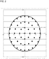
FIG. 2 is a diagram illustrating the positions where the sheet resistance of the film formed on the wafer was measured. -
FIG. 3 shows images of the crystal orientation distribution of the target of Example 1 observed via EBSPs. - The sputtering target according to the embodiments of the present invention is characterized in that an area ratio of crystal grains of which a {111} plane is oriented in a direction normal to a rolling surface (ND) is 35% or more when the ND, which is a cross section orthogonal to a sputtering surface of a target, is observed by a method using Electron Backscatter Diffraction Patterns (abbreviated EBSP(s) hereinafter). With regard to the area ratio, an EBSP device (JSM-7001 FTTLS-type field emission electron microscope/crystal orientation analyzing device OIM6.0-CCD/BS) is used to observe five positions shown in
FIG. 1 (left) and obtain an average area ratio of crystal grains of which the {111} plane is oriented in the ND with regard to the structure of the cross section (width: 2 mm, height: 6.35 mm) orthogonal to the sputtering surface as shown inFIG. 1 (right). - With tantalum having a body-centered cubic structure, the atomic close-packed direction is <111>, and the relation of the sputtering surface and the close-packed direction is important in controlling the sputter direction of the sputtered material. When the {111} plane is oriented in the direction normal to the rolling surface (ND), since the close-packed direction coincides with the direction normal to the sputtering surface, the straightness of the sputtered material can be increased. Note that the crystal grains of which the {111} plane is oriented in the ND include the crystal grains of which the orientation deviation of the {111} plane relative to the direction normal to the rolling surface (ND) is within 15°. While there is no particular limit in the upper limit value of the area ratio of the crystal grains having the {111} plane, in effect it is difficult to achieve an area ratio of 60% or higher.
- According to the embodiment of the present invention, when a direction normal to a rolling surface (ND), which is a cross section orthogonal to a sputtering surface of a target, is observed via EBSPs, a ratio {111} / {100} of an area ratio of crystal grains of which a {111} plane is oriented in the ND and an area ratio of crystal grains of which a {100} plane is oriented in the ND is preferably 2.0 or more. When the {100} plane is oriented in the direction normal to the rolling surface (ND), since the angle of the close-packed direction relative to the direction normal to the sputtering surface will become large (wide), the straightness of sputter-deposition can be further improved by lowering the ratio of this plane. As the ratio of {111} / {100} is greater, the deposition rate can be increased. Further, deposition with film thickness uniformity is also consequently enabled for some reason. Note that the crystal grains of which the {100} plane is oriented in the ND include the crystal grains of which the orientation deviation of the {100} plane relative to the direction normal to the rolling surface (ND) is within 15°. Furthermore, the area ratio of the crystal grains having the {100} plane is obtained in the same manner as the area ratio of the crystal grains having the {111} plane described above.
- According to the embodiment of the present invention, a tantalum target having a purity of 99.99% or higher is preferably used. Since impurities in the target may cause the device characteristics in a semiconductor integrated circuit to deteriorate, a tantalum target having the highest purity is preferably used. In the present invention, the purity of 99.99% (4N) means that the total amount of Na, Al, Si, K, Ti, Cr, Mn, Fe, Co, Ni, Cu, Zn, and Zr is less than 100 ppm when a Ta ingot is analyzed via glow discharge mass spectrometry (GDMS).
- The method of producing the tantalum sputtering target of the present invention is as follows.
- Foremost, tantalum is melted and cast to prepare an ingot, and the prepared ingot is thereafter forged. The ingot is subject to press forging to prepare a billet, and the billet is cut into an appropriate size and then subject to heat treatment. Furthermore, the billet is subject to first forging, first heat treatment, and second forging, divided into two, and then subject to second heat treatment, preferably at the temperature from 950 to 1100°C. The embodiments of the present invention are not particularly limited to the foregoing processes, and the number of times that forging is performed and the temperature of the heat treatment may be suitably selected upon performing the processes in order to adjust the forged structure.
- Next, 1) the obtained material is rolled consecutively two or more times in one direction, and 2) rotated 90 degrees and then additionally rolled consecutively two or more times. These processes are repeated (1→2→1→2→...) in two sets or more to subsequently obtain a predetermined plate thickness. The foregoing rolling processes are adjusted so that the structural orientation is controlled at a rolling reduction of 12% or more and the total rolling reduction is 85% or higher. The number of rolling passes contributes considerably to controlling the orientation and the {100} orientation ratio can be increased when the number of passes is greater. Meanwhile, since the rolling workload will increase when the number of passes is greater, it is important to appropriately adjust the conditions regarding the number of passes. While heat treatment may also be performed during the rolling process, it is recommended to perform the heat treatment after the final rolling as will be explained below, rather than during the rolling process. The condition of heat treatment is at 750 to 1000°C and preferably for 4 hours or longer.
- Next, the rolled material is subject to heat treatment preferably at 750 to 1000°C for 1 hour or longer, and thereafter machined into an intended shape to obtain a target. It is thereby possible to effectively destroy the forged structure and obtain a uniform and fine structure based on the rolling process. With regard to the texture of the present invention formed via the rolling process and heat treatment, the intended structural orientation can be obtained by comprehending which plane is preferentially oriented based on the EBSP method, and feeding back the results to the rolling process and heat treatment conditions.
- Now the embodiment of the present invention is explained in detail with reference to the examples. These examples are merely illustrative, and the present invention shall in no way be limited thereby. In other words, the embodiment of the present invention covers the other modes and modifications included in the technical concept of this invention.
- The evaluation method adopted in the Examples and Comparative Examples is as follows.
- The film thickness uniformity and the rate of variability thereof are evaluated using the "average value" and the "standard deviation" of the rate of variability of the film thickness (standard deviation / average value × 100) of each target life (i.e. each wafer). The target life can be represented as the integration of the power during sputtering and the total sputtering time. For example, when sputtering is performed at a power of 15 kW for 100 hours, the target life will be 1500 kWh.
- As a specific evaluation method, foremost, sputtering is performed for every 300 kWh (power of 300 kW for 1 hour), and a total of 7 wafers are deposited. Subsequently, the in-plane sheet resistance at 49 locations of each wafer is measured as shown in
FIG. 2 , the obtained values are converted into a film thickness (resistance value of tantalum is deemed 180 µΩcm), and the standard deviation and the average value of the film thickness are thereby obtained. Subsequently, the in-plane rate of variability of film thickness (%) of each wafer = standard deviation / average value × 100 is calculated, and the average value of "rate of variability of film thickness" calculated for each wafer is used as the film thickness uniformity. As the "rate of variability" of the film thickness uniformity, standard deviation/average value (corresponding to film thickness uniformity) × 100 among wafers (relative to the target life) is calculated utilizing the "rate of variability of film thickness" of each wafer obtained above. - A tantalum raw material having a purity of 99.997% was subject to electron beam melting and cast to prepare an ingot having a length of 1000 mm and a diameter of 195 mmϕ. The ingot was subject to cold press forging to obtain a diameter of 150 mmϕ, and thereafter cut to a required length to obtain a billet. Next, the billet was subject to heat treatment at a temperature of 1250°C, once again subject to cold first forging, subject to heat treatment at 1000°C, then subject to cold second forging, divided into two, and once again subject to heat treatment at 1000°C.
- Subsequently, the forged billet was subject to cold rolling. The rolling process was performed by repeating continuous rolling passes at a rolling reduction of 12% or more a total of 10 times, and thereafter performing a rolling pass at a rolling reduction of less than 12%. After the rolling process, the rolled material was subject to heat treatment at 800°C. Next, finish machining was performed to the obtained target material having a thickness of 10 mm and a diameter of 500 mmϕ to prepare a tantalum sputtering target having a thickness of 6.35 mm and a diameter of 450 mmϕ.
- The surface of the tantalum sputtering target obtained based on the foregoing processes was polished with an abrasive paper (corresponds to #2000), additionally buffed with a Polipla solution and subject to mirror finishing, and thereafter treated with a mixed liquid of hydrofluoric acid, nitric acid, and hydrochloric acid. An EBSP device (JSM-7001 FTTLS-type field emission electron microscope/crystal orientation analyzing device OIM6.0-CCD/BS) was used to observe five positions of the obtained polished surface with regard to the structure of the cross section (width: 2 mm, height: 6.35 mm) orthogonal to the sputtering surface as shown in
FIG. 1 . Moreover,FIG. 3 shows the crystal orientation distribution. Consequently, the area ratio of the crystal grains having the {111} plane was 50.5%. The area ratio of the crystal grains of which the {100} plane is oriented in the ND was 7.5%. And the ratio {111} / {100} of the foregoing area ratios was 6.73. As a result of sputtering this target, the film thickness uniformity was 2.2 and the rate of variability of the film thickness uniformity was 0.15, both of which showed effectiveness. And, the deposition rate was 6.9 A/second, which was the intended sputter rate. The results are shown in Table 1. - A forged billet was prepared in the same manner as Example 1. Next, the forged billet was subject to cold rolling. The rolling process was performed by adjusting the number of sets of continuous rolling passes at a rolling reduction of 12% or more as shown in Table 1, and thereafter performing a rolling pass at a rolling reduction of 6% or more so that the total rolling reduction will be 85% or more. After the rolling process, the rolled material was subject to heat treatment at 800°C. Next, finish machining was performed to the obtained target material having a thickness of 10 mm and a diameter of 500 mmϕ to prepare a tantalum sputtering target having a thickness of 6.35 mm and a diameter of 450 mmϕ.
- With regard to the sputtering target obtained based on the foregoing processes, the structure of the cross section orthogonal to the sputtering surface of the target was observed in the same manner as Example 1. Consequently, the area ratio of the crystal grains of which the {111} plane is oriented in the ND was 35% or more in all cases. And the ratio {111} / {100} of the foregoing area ratios was 2.0 or more in all cases. As a result of sputtering this target, the film thickness uniformity and the rate of variability of the film thickness uniformity in all cases showed effectiveness. And the deposition rate was the intended sputter rate. The results are similarly shown in Table 1.
- A forged billet was prepared in the same manner as Example 1. Next, the forged billet was subject to cold rolling. The rolling process was performed by adjusting the number of sets of continuous rolling passes at a rolling reduction of 12% or more as shown in Table 1, and thereafter performing a rolling pass at a rolling reduction of 6% or more so that the total rolling reduction will be 85% or more. After the rolling process, the rolled material was subject to heat treatment at 800°C. Next, finish machining was performed to the obtained target material having a thickness of 10 mm and a diameter of 350 mmϕ to prepare a tantalum sputtering target having a thickness of 6.35 mm and a diameter of 320 mmϕ.
- With regard to the sputtering target obtained based on the foregoing processes, the structure of the cross section orthogonal to the sputtering surface of the target was observed in the same manner as Example 1. As a result, the area ratio of the crystal grains of which the {111} plane is oriented in the ND was less than 35% in all cases. And the ratio {111} / {100} of the foregoing area ratios was more than 2.0 in all cases. As a result of sputtering this target, the film thickness uniformity and/or the rate of variability of the film thickness uniformity deteriorated in all cases. Moreover, the sputter rate was high. The results are similarly shown in Table 1.
Table 1 Number of continuous roll passes of 12% or more (111) area ratio (100) area ratio (111)/(100) Film thickness uniformity Deposition rate: (Å/second) Evaluation Example 1 10 50.5 7.5 6.73 2.2 6.9 ⊚ Example 2 9 48.5 8.6 5.64 2.3 6.7 ⊚ Example 3 8 44.1 12.9 3.42 2.4 6.4 ○ Example 4 7 36.9 13.6 2.71 2.4 6.5 ○ Example 5 6 36.7 18.3 2.01 2.6 6.4 ○ Comparative Example 5 34.9 23.1 1.51 2.7 6.2 Δ Comparative Example 2 4 32.4 27.7 1.17 2.7 6.2 Δ Comparative Example 3 3 30.8 22.7 1.36 2.8 6.1 × Comparative Example 4 2 27.2 27.4 0.99 2.7 6.3 Δ Comparative Example 5 1 24.3 29.5 0.82 2.9 6 × -
⊚→ Deposition rate: 6.6 or more Δ→ Deposition rate: 6.2 to less than 6.4 Film thickness uniformity: Less than 2.4 Film thickness uniformity: 2.6 to less than 2.8 ○→ Deposition rate: 6.4 to less than 6.6 ×→- Deposition rate: Less than 6.2 Film thickness uniformity: 2.4 to less than 2.6 Film thickness uniformity: 2.8 to less than 3.0 - According to the embodiment of the present invention, by causing the structural orientation of a tantalum sputtering target to be a predetermined state, the straightness of the sputtered material can be increased and the sputtered material can be uniformly deposited on the wafer surface even under high-power sputtering conditions. The increase in the straightness of the sputtered material can eventually achieve both uniform film thickness and the throughput of deposition. Embodiments of the present invention provide a tantalum sputtering target that is useful in forming a thin film of an element wiring of a semiconductor integrated circuit.
Claims (2)
- A tantalum sputtering target comprising, an area ratio of crystal grains of which a {111} plane is oriented in a direction normal to a rolling surface (ND) is 35% or more when the ND, which is a cross section orthogonal to a sputtering surface of a target, is observed via Electron Backscatter Diffraction Patterns.
- The tantalum sputtering target according to claim 1, wherein a ratio {111} / {100} of an area ratio of crystal grains of which a {111} plane is oriented in a direction normal to a rolling surface (ND) and an area ratio of crystal grains of which a {100} plane is oriented in the ND is 2.0 or more when the ND, which is a cross section orthogonal to a sputtering surface of a target, is observed via Electron Backscatter Diffraction Patterns.
Applications Claiming Priority (2)
| Application Number | Priority Date | Filing Date | Title |
|---|---|---|---|
| JP2015104295 | 2015-05-22 | ||
| PCT/JP2016/064537 WO2016190159A1 (en) | 2015-05-22 | 2016-05-17 | Tantalum sputtering target, and production method therefor |
Publications (3)
| Publication Number | Publication Date |
|---|---|
| EP3260572A1 true EP3260572A1 (en) | 2017-12-27 |
| EP3260572A4 EP3260572A4 (en) | 2018-08-01 |
| EP3260572B1 EP3260572B1 (en) | 2026-04-15 |
Family
ID=57392751
Family Applications (1)
| Application Number | Title | Priority Date | Filing Date |
|---|---|---|---|
| EP16799865.7A Active EP3260572B1 (en) | 2015-05-22 | 2016-05-17 | Tantalum sputtering target, and production method therefor |
Country Status (9)
| Country | Link |
|---|---|
| US (1) | US10570505B2 (en) |
| EP (1) | EP3260572B1 (en) |
| JP (1) | JP6293928B2 (en) |
| KR (1) | KR102074047B1 (en) |
| CN (1) | CN107532287B (en) |
| IL (1) | IL255349B (en) |
| SG (1) | SG11201708112TA (en) |
| TW (1) | TWI676691B (en) |
| WO (1) | WO2016190159A1 (en) |
Families Citing this family (3)
| Publication number | Priority date | Publication date | Assignee | Title |
|---|---|---|---|---|
| KR20170091738A (en) | 2015-05-22 | 2017-08-09 | 제이엑스금속주식회사 | Tantalum sputtering target, and production method therefor |
| CN109338316B (en) * | 2018-09-12 | 2020-04-28 | 中南大学 | Ultra-pure tantalum with controllable structure and texture and preparation method and application thereof |
| CN114892136A (en) * | 2022-05-25 | 2022-08-12 | 同创(丽水)特种材料有限公司 | Tantalum target material and preparation method and application thereof |
Family Cites Families (39)
| Publication number | Priority date | Publication date | Assignee | Title |
|---|---|---|---|---|
| JPH1180942A (en) | 1997-09-10 | 1999-03-26 | Japan Energy Corp | Ta sputter target, method of manufacturing the same and assembly |
| US6348139B1 (en) | 1998-06-17 | 2002-02-19 | Honeywell International Inc. | Tantalum-comprising articles |
| US6348113B1 (en) * | 1998-11-25 | 2002-02-19 | Cabot Corporation | High purity tantalum, products containing the same, and methods of making the same |
| JP2001020065A (en) | 1999-07-07 | 2001-01-23 | Hitachi Metals Ltd | Sputtering target, method for producing the same, and refractory metal powder material |
| US6331233B1 (en) | 2000-02-02 | 2001-12-18 | Honeywell International Inc. | Tantalum sputtering target with fine grains and uniform texture and method of manufacture |
| JP2001295035A (en) | 2000-04-11 | 2001-10-26 | Toshiba Corp | Sputtering target and method for manufacturing the same |
| EP1366203B1 (en) | 2001-02-20 | 2006-09-13 | H. C. Starck, Inc. | Refractory metal plates with uniform texture and methods of making the same |
| JP4817536B2 (en) | 2001-06-06 | 2011-11-16 | 株式会社東芝 | Sputter target |
| US7081148B2 (en) * | 2001-09-18 | 2006-07-25 | Praxair S.T. Technology, Inc. | Textured-grain-powder metallurgy tantalum sputter target |
| JP4883546B2 (en) | 2002-09-20 | 2012-02-22 | Jx日鉱日石金属株式会社 | Method for manufacturing tantalum sputtering target |
| JP4263900B2 (en) | 2002-11-13 | 2009-05-13 | 日鉱金属株式会社 | Ta sputtering target and manufacturing method thereof |
| US7067197B2 (en) * | 2003-01-07 | 2006-06-27 | Cabot Corporation | Powder metallurgy sputtering targets and methods of producing same |
| EP2253731B1 (en) | 2003-04-01 | 2019-07-31 | JX Nippon Mining & Metals Corporation | Tantalum spattering target |
| JP4593475B2 (en) | 2003-11-06 | 2010-12-08 | Jx日鉱日石金属株式会社 | Tantalum sputtering target |
| US8252126B2 (en) | 2004-05-06 | 2012-08-28 | Global Advanced Metals, Usa, Inc. | Sputter targets and methods of forming same by rotary axial forging |
| US7998287B2 (en) * | 2005-02-10 | 2011-08-16 | Cabot Corporation | Tantalum sputtering target and method of fabrication |
| EP1876258A4 (en) | 2005-04-28 | 2008-08-13 | Nippon Mining Co | SPRAY TARGET |
| JP4949259B2 (en) | 2005-10-04 | 2012-06-06 | Jx日鉱日石金属株式会社 | Sputtering target |
| JP5389802B2 (en) | 2007-08-06 | 2014-01-15 | エイチ.シー. スターク インコーポレイテッド | Refractory metal plate with improved tissue uniformity |
| US8250895B2 (en) | 2007-08-06 | 2012-08-28 | H.C. Starck Inc. | Methods and apparatus for controlling texture of plates and sheets by tilt rolling |
| JPWO2009107763A1 (en) * | 2008-02-29 | 2011-07-07 | 新日鉄マテリアルズ株式会社 | Metal-based sputtering target material |
| WO2010051040A1 (en) * | 2008-11-03 | 2010-05-06 | Tosoh Smd, Inc. | Method of making a sputter target and sputter targets made thereby |
| CN102356179B (en) | 2009-05-22 | 2013-10-30 | 吉坤日矿日石金属株式会社 | Tantalum sputtering target |
| KR101362025B1 (en) | 2009-05-29 | 2014-02-13 | 아리조나 보드 오브 리젠츠 퍼 앤 온 비하프 오브 아리조나 스테이트 유니버시티 | Method of providing a flexible semiconductor device at high temperatures and flexible semiconductor device thereof |
| WO2011018970A1 (en) | 2009-08-11 | 2011-02-17 | Jx日鉱日石金属株式会社 | Tantalum sputtering target |
| KR101338758B1 (en) | 2009-08-11 | 2013-12-06 | 제이엑스 닛코 닛세키 킨조쿠 가부시키가이샤 | Tantalum sputtering target |
| US9017493B2 (en) | 2009-08-12 | 2015-04-28 | Ulvac, Inc. | Method of manufacturing a sputtering target and sputtering target |
| KR20150039218A (en) | 2009-11-17 | 2015-04-09 | 가부시끼가이샤 도시바 | Tantalum sputtering target, method for manufacturing tantalum sputtering target, and method for manufacturing semiconductor device |
| KR20130008089A (en) | 2010-08-09 | 2013-01-21 | 제이엑스 닛코 닛세키 킨조쿠 가부시키가이샤 | Tantalum spattering target |
| KR20130037215A (en) | 2010-08-09 | 2013-04-15 | 제이엑스 닛코 닛세키 킨조쿠 가부시키가이샤 | Tantalum spattering target |
| US20140242401A1 (en) | 2011-11-30 | 2014-08-28 | Jx Nippon Mining & Metals Corporation | Tantalum Sputtering Target and Method for Manufacturing Same |
| CN104204282B (en) | 2012-03-21 | 2017-05-24 | 吉坤日矿日石金属株式会社 | Tantalum sputtering target, method for manufacturing same, and barrier film for semiconductor wiring formed by using target |
| KR101950549B1 (en) | 2012-12-19 | 2019-02-20 | 제이엑스금속주식회사 | Tantalum sputtering target and method for producing same |
| EP2878700B1 (en) | 2012-12-19 | 2021-01-20 | JX Nippon Mining & Metals Corporation | Method for producing tantalum sputtering target |
| KR20170092706A (en) | 2013-03-04 | 2017-08-11 | 제이엑스금속주식회사 | Tantalum sputtering target and production method therefor |
| KR20160052664A (en) | 2013-10-01 | 2016-05-12 | 제이엑스 킨조쿠 가부시키가이샤 | Tantalum sputtering target |
| WO2015146516A1 (en) | 2014-03-27 | 2015-10-01 | Jx日鉱日石金属株式会社 | Tantalum sputtering target and production method therefor |
| CN104480439A (en) * | 2014-12-31 | 2015-04-01 | 宁夏东方钽业股份有限公司 | Preparation process of tantalum target material |
| KR20170091738A (en) | 2015-05-22 | 2017-08-09 | 제이엑스금속주식회사 | Tantalum sputtering target, and production method therefor |
-
2016
- 2016-05-17 US US15/571,562 patent/US10570505B2/en active Active
- 2016-05-17 CN CN201680023081.4A patent/CN107532287B/en active Active
- 2016-05-17 SG SG11201708112TA patent/SG11201708112TA/en unknown
- 2016-05-17 WO PCT/JP2016/064537 patent/WO2016190159A1/en not_active Ceased
- 2016-05-17 EP EP16799865.7A patent/EP3260572B1/en active Active
- 2016-05-17 KR KR1020177029390A patent/KR102074047B1/en active Active
- 2016-05-17 JP JP2016566834A patent/JP6293928B2/en active Active
- 2016-05-19 TW TW105115508A patent/TWI676691B/en active
-
2017
- 2017-10-31 IL IL255349A patent/IL255349B/en unknown
Also Published As
| Publication number | Publication date |
|---|---|
| JP6293928B2 (en) | 2018-03-14 |
| WO2016190159A1 (en) | 2016-12-01 |
| CN107532287B (en) | 2019-11-05 |
| EP3260572A4 (en) | 2018-08-01 |
| IL255349A0 (en) | 2017-12-31 |
| US20180105926A1 (en) | 2018-04-19 |
| TW201704493A (en) | 2017-02-01 |
| KR102074047B1 (en) | 2020-02-05 |
| EP3260572B1 (en) | 2026-04-15 |
| SG11201708112TA (en) | 2017-11-29 |
| KR20170127548A (en) | 2017-11-21 |
| IL255349B (en) | 2021-09-30 |
| TWI676691B (en) | 2019-11-11 |
| JPWO2016190159A1 (en) | 2017-06-15 |
| CN107532287A (en) | 2018-01-02 |
| US10570505B2 (en) | 2020-02-25 |
Similar Documents
| Publication | Publication Date | Title |
|---|---|---|
| EP1609881B1 (en) | Method of manufacturing a tantalum sputtering target | |
| EP1681368B1 (en) | Method to produce a tantalum sputtering target | |
| US20050155856A1 (en) | Tantalum sputtering target and method for preparation thereof | |
| US12180577B2 (en) | Titanium sputtering target, production method therefor, and method for producing titanium-containing thin film | |
| EP3211118B1 (en) | Tantalum sputtering target, and production method therefor | |
| EP2878700B1 (en) | Method for producing tantalum sputtering target | |
| EP3260572A1 (en) | Tantalum sputtering target, and production method therefor | |
| CN109154074B (en) | Tantalum sputtering target | |
| KR20180004214A (en) | Al alloy sputtering target | |
| JP2009108412A (en) | Target |
Legal Events
| Date | Code | Title | Description |
|---|---|---|---|
| STAA | Information on the status of an ep patent application or granted ep patent |
Free format text: STATUS: THE INTERNATIONAL PUBLICATION HAS BEEN MADE |
|
| PUAI | Public reference made under article 153(3) epc to a published international application that has entered the european phase |
Free format text: ORIGINAL CODE: 0009012 |
|
| STAA | Information on the status of an ep patent application or granted ep patent |
Free format text: STATUS: REQUEST FOR EXAMINATION WAS MADE |
|
| 17P | Request for examination filed |
Effective date: 20170920 |
|
| AK | Designated contracting states |
Kind code of ref document: A1 Designated state(s): AL AT BE BG CH CY CZ DE DK EE ES FI FR GB GR HR HU IE IS IT LI LT LU LV MC MK MT NL NO PL PT RO RS SE SI SK SM TR |
|
| AX | Request for extension of the european patent |
Extension state: BA ME |
|
| A4 | Supplementary search report drawn up and despatched |
Effective date: 20180629 |
|
| RIC1 | Information provided on ipc code assigned before grant |
Ipc: C22F 1/18 20060101ALI20180625BHEP Ipc: C23C 14/34 20060101AFI20180625BHEP Ipc: C22C 27/02 20060101ALI20180625BHEP Ipc: B21J 1/02 20060101ALI20180625BHEP Ipc: C22F 1/00 20060101ALI20180625BHEP |
|
| DAV | Request for validation of the european patent (deleted) | ||
| DAX | Request for extension of the european patent (deleted) | ||
| RAP1 | Party data changed (applicant data changed or rights of an application transferred) |
Owner name: JX NIPPON MINING & METALS CORPORATION |
|
| STAA | Information on the status of an ep patent application or granted ep patent |
Free format text: STATUS: EXAMINATION IS IN PROGRESS |
|
| 17Q | First examination report despatched |
Effective date: 20201112 |
|
| GRAP | Despatch of communication of intention to grant a patent |
Free format text: ORIGINAL CODE: EPIDOSNIGR1 |
|
| STAA | Information on the status of an ep patent application or granted ep patent |
Free format text: STATUS: GRANT OF PATENT IS INTENDED |
|
| RIC1 | Information provided on ipc code assigned before grant |
Ipc: C23C 14/34 20060101AFI20251106BHEP Ipc: B21J 1/00 20060101ALI20251106BHEP Ipc: B21J 1/02 20060101ALI20251106BHEP Ipc: C22C 27/02 20060101ALI20251106BHEP Ipc: C22F 1/18 20060101ALI20251106BHEP |
|
| INTG | Intention to grant announced |
Effective date: 20251118 |
|
| RIN1 | Information on inventor provided before grant (corrected) |
Inventor name: NAGATSU, KOTARO Inventor name: SENDA, SHINICHIRO |
|
| GRAJ | Information related to disapproval of communication of intention to grant by the applicant or resumption of examination proceedings by the epo deleted |
Free format text: ORIGINAL CODE: EPIDOSDIGR1 |
|
| STAA | Information on the status of an ep patent application or granted ep patent |
Free format text: STATUS: EXAMINATION IS IN PROGRESS |
|
| GRAP | Despatch of communication of intention to grant a patent |
Free format text: ORIGINAL CODE: EPIDOSNIGR1 |
|
| STAA | Information on the status of an ep patent application or granted ep patent |
Free format text: STATUS: GRANT OF PATENT IS INTENDED |
|
| INTC | Intention to grant announced (deleted) | ||
| INTG | Intention to grant announced |
Effective date: 20260119 |
|
| RAP3 | Party data changed (applicant data changed or rights of an application transferred) |
Owner name: JX ADVANCED METALS CORPORATION |
|
| GRAS | Grant fee paid |
Free format text: ORIGINAL CODE: EPIDOSNIGR3 |
|
| GRAA | (expected) grant |
Free format text: ORIGINAL CODE: 0009210 |
|
| STAA | Information on the status of an ep patent application or granted ep patent |
Free format text: STATUS: THE PATENT HAS BEEN GRANTED |
|
| AK | Designated contracting states |
Kind code of ref document: B1 Designated state(s): AL AT BE BG CH CY CZ DE DK EE ES FI FR GB GR HR HU IE IS IT LI LT LU LV MC MK MT NL NO PL PT RO RS SE SI SK SM TR |
|
| P01 | Opt-out of the competence of the unified patent court (upc) registered |
Free format text: CASE NUMBER: UPC_APP_0008932_3260572/2026 Effective date: 20260306 |
|
| REG | Reference to a national code |
Ref country code: CH Ref legal event code: F10 Free format text: ST27 STATUS EVENT CODE: U-0-0-F10-F00 (AS PROVIDED BY THE NATIONAL OFFICE) Effective date: 20260415 Ref country code: GB Ref legal event code: FG4D |