EP3258601A1 - Power supply shut-off device - Google Patents
Power supply shut-off device Download PDFInfo
- Publication number
- EP3258601A1 EP3258601A1 EP17175826.1A EP17175826A EP3258601A1 EP 3258601 A1 EP3258601 A1 EP 3258601A1 EP 17175826 A EP17175826 A EP 17175826A EP 3258601 A1 EP3258601 A1 EP 3258601A1
- Authority
- EP
- European Patent Office
- Prior art keywords
- pair
- field effect
- effect transistors
- terminals
- temperature detection
- Prior art date
- Legal status (The legal status is an assumption and is not a legal conclusion. Google has not performed a legal analysis and makes no representation as to the accuracy of the status listed.)
- Granted
Links
Images

Classifications
-
- H—ELECTRICITY
- H03—ELECTRONIC CIRCUITRY
- H03K—PULSE TECHNIQUE
- H03K17/00—Electronic switching or gating, i.e. not by contact-making and –breaking
- H03K17/18—Modifications for indicating state of switch
-
- B—PERFORMING OPERATIONS; TRANSPORTING
- B60—VEHICLES IN GENERAL
- B60L—PROPULSION OF ELECTRICALLY-PROPELLED VEHICLES; SUPPLYING ELECTRIC POWER FOR AUXILIARY EQUIPMENT OF ELECTRICALLY-PROPELLED VEHICLES; ELECTRODYNAMIC BRAKE SYSTEMS FOR VEHICLES IN GENERAL; MAGNETIC SUSPENSION OR LEVITATION FOR VEHICLES; MONITORING OPERATING VARIABLES OF ELECTRICALLY-PROPELLED VEHICLES; ELECTRIC SAFETY DEVICES FOR ELECTRICALLY-PROPELLED VEHICLES
- B60L3/00—Electric devices on electrically-propelled vehicles for safety purposes; Monitoring operating variables, e.g. speed, deceleration or energy consumption
- B60L3/0023—Detecting, eliminating, remedying or compensating for drive train abnormalities, e.g. failures within the drive train
-
- G—PHYSICS
- G01—MEASURING; TESTING
- G01R—MEASURING ELECTRIC VARIABLES; MEASURING MAGNETIC VARIABLES
- G01R31/00—Arrangements for testing electric properties; Arrangements for locating electric faults; Arrangements for electrical testing characterised by what is being tested not provided for elsewhere
- G01R31/327—Testing of circuit interrupters, switches or circuit-breakers
- G01R31/3277—Testing of circuit interrupters, switches or circuit-breakers of low voltage devices, e.g. domestic or industrial devices, such as motor protections, relays, rotation switches
-
- H—ELECTRICITY
- H02—GENERATION; CONVERSION OR DISTRIBUTION OF ELECTRIC POWER
- H02H—EMERGENCY PROTECTIVE CIRCUIT ARRANGEMENTS
- H02H3/00—Emergency protective circuit arrangements for automatic disconnection directly responsive to an undesired change from normal electric working condition with or without subsequent reconnection ; integrated protection
- H02H3/02—Details
- H02H3/04—Details with warning or supervision in addition to disconnection, e.g. for indicating that protective apparatus has functioned
- H02H3/044—Checking correct functioning of protective arrangements, e.g. by simulating a fault
-
- H—ELECTRICITY
- H03—ELECTRONIC CIRCUITRY
- H03K—PULSE TECHNIQUE
- H03K17/00—Electronic switching or gating, i.e. not by contact-making and –breaking
- H03K17/51—Electronic switching or gating, i.e. not by contact-making and –breaking characterised by the components used
- H03K17/56—Electronic switching or gating, i.e. not by contact-making and –breaking characterised by the components used by the use, as active elements, of semiconductor devices
- H03K17/687—Electronic switching or gating, i.e. not by contact-making and –breaking characterised by the components used by the use, as active elements, of semiconductor devices the devices being field-effect transistors
- H03K17/6871—Electronic switching or gating, i.e. not by contact-making and –breaking characterised by the components used by the use, as active elements, of semiconductor devices the devices being field-effect transistors the output circuit comprising more than one controlled field-effect transistor
- H03K17/6874—Electronic switching or gating, i.e. not by contact-making and –breaking characterised by the components used by the use, as active elements, of semiconductor devices the devices being field-effect transistors the output circuit comprising more than one controlled field-effect transistor in a symmetrical configuration
-
- H—ELECTRICITY
- H03—ELECTRONIC CIRCUITRY
- H03K—PULSE TECHNIQUE
- H03K2217/00—Indexing scheme related to electronic switching or gating, i.e. not by contact-making or -breaking covered by H03K17/00
- H03K2217/0009—AC switches, i.e. delivering AC power to a load
Definitions
- Embodiments disclosed herein relate to a power supply shut-off device that controls energization of a power.
- relays have been used in view of safety and operability.
- the relays include a relay configured using a semiconductor switch, as disclosed in, for example, Journal of Technical Disclosure No. 2012-504284 published by the Japan Institute for Promoting Invention and Innovation (Reference 1).
- a pair of field effect transistors are provided in a power supply line in a state where drain terminals of the pair of field effect transistors are connected to each other, and it is diagnosed whether the pair of field effect transistors are failed, based on a voltage value obtained by dividing voltages of the drain terminals by two resistors (hereinafter, referred to as a "divided voltage value").
- the failure diagnosis of the field effect transistors is performed based on a divided voltage value obtained when both the pair of field effect transistors are in the OFF state, a divided voltage value obtained when only one of the pair of field effect transistors is in the ON state, and a divided voltage value obtained when both the pair of field effect transistors are in the ON state.
- the failure diagnosis according to the technology disclosed in Reference 1 may not be actually performed while supplying power to the downstream side via the power supply shut-off device, and needs to be performed prior to using the power shut-off device. Further, since the failure diagnosis is performed by appropriately switching the operations of the pair of field effect transistors, the failure diagnosis takes time.
- a power supply shut-off device includes: a pair of field effect transistors that are connected to each other at source terminals thereof, and have same channel polarity; an input terminal that is connected to a drain terminal of one of the pair of field effect transistors and supplied with a power from a battery; an output terminal that is connected to a drain terminal of the other of the pair of field effect transistors and supplies the power to a load; a pair of temperature detection elements that are installed adjacent to the drain terminals of the pair of field effect transistors, respectively; and a diagnosis unit that performs failure diagnosis of the pair of field effect transistors based on detection results by the pair of temperature detection elements.
- parasitic diodes formed within the field effect transistors may be arranged such that the rectifying current directions of the parasitic diodes are different from each other. Accordingly, in a case where the field effect transistors are failed in an open mode, when the direction in which current flows at that time follows the reverse direction of the parasitic diodes, no voltage is generated at the anode sides of the parasitic diodes, and thus, it may be determined that the field effect transistor of which the drain terminal is connected to the output terminal is failed.
- the temperature of the field effect transistors increases since the parasitic diodes generate heat due to the forward voltage of the parasitic diodes and the flowing current, and thus, it may be determined that the field effect transistor of which the drain terminal is connected to the input terminal is failed, based on detection results by the temperature detection elements.
- the failure diagnosis may be performed while actually using the power supply shut-off device.
- the pair of temperature detection elements are connected to the drain terminals of the pair of field effect transistors, respectively.
- the heat of the field effect transistors may be directly transferred to the temperature detection elements via the drain terminals. Accordingly, the temperature of the field effect transistors which is relatively closer to the junction temperature of the PN junction may be detected.
- the power supply shut-off device further includes a board on which the pair of field effect transistors are mounted, and on the board, the width of a pattern to which the source terminals are connected is formed narrower than the width of a pattern to which the drain terminals are connected.
- the patterns to which the terminals of one of the field effect transistors are connected and the patterns to which the terminals of the other of the field effect transistors are connected are arranged symmetrically with each other.
- the patterns to which the terminals of one of the field effect transistors are connected and the patterns to which the terminals of the other of the field effect transistors are connected may be arranged to be identical to each other.
- the influence of the difference in patterns with respect to the temperature environments of the pair of field effect transistors may be reduced.
- the field effect transistors are disposed adjacent to each other.
- the heat of the field effect transistor is often radiated from the drain terminal.
- the heat generation of the field effect transistors may be appropriately detected.
- a power supply shut-off device disclosed here is configured such that failure diagnosis may be performed even during use thereof.
- a power supply shut-off device 1 of an exemplary embodiment will be described.
- Fig. 1 illustrates a circuit diagram of the power supply shut-off device 1.
- the power supply shut-off device 1 includes a pair of field effect transistors 10 (hereinafter, referred to as "FETs"), an input terminal 20, an output terminal 30, a pair of temperature detection elements 40, a diagnosis unit 50, and a controller 60.
- the diagnosis unit 50 is constructed in hardware, software, or both the hardware and the software using a CPU as a core member.
- the pair of FETs 10 include an FET 10A and an FET 10B, and source terminals of the FET 10A and the FET 10B are connected to each other. Accordingly, the pair of FETs 10 are connected in series. Further, the pair of FETs 10 are configured using those having the same channel polarity. The same channel polarity indicates that when the FET 10A is configured using a P-type FET, the FET 10B is also configured using a P-type FET, and when the FET 10A is configured using an N-type FET, the FET 10B is also configured using an N-type FET. In this exemplary embodiment, as illustrated in Fig. 1 , the pair of FETs 10 are configured using P-type FETs.
- the drain terminal of the FET 10A is connected to the input terminal 20.
- Power is supplied to the input terminal 20 from a battery 2.
- the power from the battery 2 is a power to be controlled by the power supply shut-off device 1.
- the battery 2 may be, for example, a battery mounted on a vehicle.
- the drain terminal of the FET 10B is connected to the output terminal 30.
- a load 3 to which the power from the battery 2 is supplied is connected to the output terminal 30.
- the load 3 is, for example, a motor or an inductive load such as a solenoid valve.
- parasitic diodes 11 A and 11 B are formed in a state where the anodes of the diodes 11 A and 11 B are connected to the drain terminals of the FETs 10A and 10B, respectively, and the cathodes of the diodes 11 A and 11 B are connected to the source terminals of the FETs 10A and 10B, respectively.
- transistors 12A and 12B npn-type transistors in this exemplary embodiment
- the collector terminals of transistors 12A and 12B are connected to the gate terminals of the pair of FETs 10.
- the transistors 12A and 12B are configured such that current may be supplied to the base terminals thereof from the controller 60. Accordingly, when current is supplied to the base terminals of the transistors 12A and 12B from the controller 60, each of the pair of FETs 10 becomes an ON state.
- the pair of temperature detection elements 40 include a temperature detection element 40A and a temperature detection element 40B.
- One terminal of the temperature detection element 40A is connected to the drain terminal of the FET 10A, and the other terminal of the temperature detection element 40A is connected to one terminal of a resistor 41 A of which the other terminal is grounded and which has a predetermined resistance value.
- One terminal of the temperature detection element 40B is connected to the drain terminal of the FET 10B, and the other terminal of the temperature detection element 40B is connected to one terminal of a resistor 41 B of which the other terminal is grounded and which has a predetermined resistance value.
- the pair of temperature detection elements 40 are configured using thermistors each having a characteristic that the resistance value increases with a temperature rise.
- the diagnosis unit 50 performs failure diagnosis of the pair of FETs 10 based on detection results by the pair of temperature detection elements 40. Specifically, when current is supplied to the base terminals of the transistors 12A and 12B such that the pair of FETs 10 become the ON state, the controller 60 may appropriately diagnose whether the pair of FETs 10 are failed, based on a result of comparison of the voltage value divided by the temperature detection element 40A and the resistor 41 A and the voltage value divided by the temperature detection element 40B and the resistor 41 B, with a predetermined value obtained by dividing the voltage from the battery 2 by the resistance values of the respective elements.
- the diagnosis unit 50 may diagnose whether the FET 10A is failed, based on the detection result by the temperature detection element 40A.
- the diagnosis unit 50 may diagnose whether the FET 10 B is failed, based on the detection result by the temperature detection element 40B.
- a voltage may be applied from the side of the load 3 to the drain terminal of the FET 10B via the output terminal 30.
- current caused by the corresponding voltage flows to the ground via the diode 11 B and the transistor 12B, and the diode 11 B generates heat by the current and the forward voltage of the diode 11 B. Due to the heat, the resistance value of the temperature detection element 40B increases, and hence, the voltage value divided by the temperature detection element 40B and the resistor 41 B becomes smaller than the predetermined value.
- the diagnosis section 50 may diagnose whether the FET 10A is failed, based on the detection result by the temperature detection element 40A.
- the power supply shut-off device 1 disclosed here determines whether the pair of FETs 10 are failed, based on the detection results by the pair of temperature detection elements 40. Especially, it is key that the resistance values of the temperature detection elements 40 change with the heat generation of the diodes 11 A and 11 B. Thus, the power supply shut-off device 1 may be configured as described below.
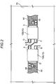
- Fig. 2 is a plan view of a portion of the board 70 on which the pair of FETs 10 are mounted.
- the board 70 for example, a printed board may be used.
- the drain terminal is denoted by symbol D
- the source terminal is denoted by symbol S
- the gate terminal is denoted by symbol G.
- the hatched portion is a wiring pattern.
- the pair of temperature detection elements 40 are installed adjacent to the drain terminals D of the pair of FETs 10, respectively.
- Each of the FETs 10 is configured by dicing a chip formed on a semiconductor wafer and sealing the chip with a resin.
- the drain terminals D are installed on the back surfaces of the chips, and the source terminals S and the gate terminals G are installed on the front surface of the chip. Accordingly, since the heat of the FETs 10 is often radiated from the drain terminals D, the temperature detection elements 40 are required to be installed adjacent to the drain terminals D so as to check the heat generation of the FETs 10.
- the width of a pattern 91 to which the source terminals S are connected is formed narrower than the width of a pattern 92 to which the drain terminals D are connected. Accordingly, heat radiation from the pattern 91 connected to the source terminals S may be reduced, and mutual heat transfer between the pair of FETs 10 may be suppressed.
- the FETs 10A and 10B are arranged adjacent to each other. Accordingly, the respective temperature environments of the pair of FETs 10 may be equalized.
- the patterns to which the terminals of the FET 10A are connected and the patterns to which the terminals of the FET 10B are connected are arranged symmetrically with each other. As illustrated in Fig. 2 , the arrangements of the terminals of the FETs 10 are the same in the FETs 10A and 10B. Accordingly, it is required that, on the board 70, the patterns to which the terminals of the FET 10A are connected and the patterns to which the terminals of the FET 10B are connected are arranged to be point-symmetrical with each other. Therefore, the respective temperature environments of the pair of FETs 10 may be equalized.
- the pair of FETs 10 are configured using P-type FETs has been described.
- the pair of FETs 10 may be configured using N-type FETs.
- the temperature detection elements 40 may be configured using temperature detection elements other than thermistors.
- the pair of temperature detection elements 40 are connected to the drain terminals of the pair of FETs 10, respectively.
- the temperature detection elements 40 may be configured such that a resistor having a predetermined resistance value is installed between one terminal of each of the pair of temperature detection elements 40 and the drain terminal of each of the pair of FETs 10, and the other terminal of each of the pair of temperature detection elements 40 is grounded.
- temperature detection elements each having a characteristic that the resistance value decreases with the temperature rise may be used as the pair of temperature detection elements 40.
- the voltage value divided by the temperature detection element 40A and the resistor 41A or the voltage value divided by the temperature detection element 40B and the resistor 41 B may be made smaller than the predetermined value, according to the heat generation of the diode 11A or 11 B. Therefore, in this case as well, it may be diagnosed whether the FETs 10A and 10B are failed, based on the detection results by the temperature detection elements 40A and 40B.
- the width of the pattern to which the source terminals are connected is formed narrower than the width of the pattern to which the drain terminals are connected.
- the width of the pattern to which the source terminals are connected and the width of the pattern to which the drain terminals are connected may be configured to be the same.
- the width of the pattern to which the source terminals are connected may be formed wider than the width of the pattern to which the drain terminals are connected.
- the patterns to which the terminals of the FET 10A are connected and the patterns to which the terminals of the FET 10B are connected are arranged symmetrically with each other.
- the patterns to which the terminals of the FET 10A are connected and the patterns to which the terminals of the FET 10B are connected may be asymmetrically arranged.
- the FETs 10A and 10B are arranged adjacent to each other.
- the FETs 10A and 10B may be arranged to be spaced apart from each other.
- the embodiments disclosed here may be used for a power supply shut-off device that controls energization of a power.
Abstract
Description
- Embodiments disclosed herein relate to a power supply shut-off device that controls energization of a power.
- For example, in electric equipment of related art, relays have been used in view of safety and operability. The relays include a relay configured using a semiconductor switch, as disclosed in, for example, Journal of Technical Disclosure No.
2012-504284 published by the Japan Institute for Promoting Invention and Innovation (Reference 1). - In the power supply shut-off device disclosed in Reference 1, a pair of field effect transistors are provided in a power supply line in a state where drain terminals of the pair of field effect transistors are connected to each other, and it is diagnosed whether the pair of field effect transistors are failed, based on a voltage value obtained by dividing voltages of the drain terminals by two resistors (hereinafter, referred to as a "divided voltage value").
- In the power supply shut-off device disclosed in Reference 1, the failure diagnosis of the field effect transistors is performed based on a divided voltage value obtained when both the pair of field effect transistors are in the OFF state, a divided voltage value obtained when only one of the pair of field effect transistors is in the ON state, and a divided voltage value obtained when both the pair of field effect transistors are in the ON state. Hence, the failure diagnosis according to the technology disclosed in Reference 1 may not be actually performed while supplying power to the downstream side via the power supply shut-off device, and needs to be performed prior to using the power shut-off device. Further, since the failure diagnosis is performed by appropriately switching the operations of the pair of field effect transistors, the failure diagnosis takes time.
- Thus, a need exists for a power supply shut-off device capable of performing failure diagnosis during actual use thereof.
- A power supply shut-off device according to an aspect of this disclosure includes: a pair of field effect transistors that are connected to each other at source terminals thereof, and have same channel polarity; an input terminal that is connected to a drain terminal of one of the pair of field effect transistors and supplied with a power from a battery; an output terminal that is connected to a drain terminal of the other of the pair of field effect transistors and supplies the power to a load; a pair of temperature detection elements that are installed adjacent to the drain terminals of the pair of field effect transistors, respectively; and a diagnosis unit that performs failure diagnosis of the pair of field effect transistors based on detection results by the pair of temperature detection elements.
- With this configuration, since the source terminals of the pair of field effect transistors are connected to each other, parasitic diodes formed within the field effect transistors, respectively, may be arranged such that the rectifying current directions of the parasitic diodes are different from each other. Accordingly, in a case where the field effect transistors are failed in an open mode, when the direction in which current flows at that time follows the reverse direction of the parasitic diodes, no voltage is generated at the anode sides of the parasitic diodes, and thus, it may be determined that the field effect transistor of which the drain terminal is connected to the output terminal is failed. Meanwhile, when the direction in which current flows at the time when the field electric transistors are failed in the open mode follows the forward direction of the parasitic diodes, the temperature of the field effect transistors increases since the parasitic diodes generate heat due to the forward voltage of the parasitic diodes and the flowing current, and thus, it may be determined that the field effect transistor of which the drain terminal is connected to the input terminal is failed, based on detection results by the temperature detection elements. With this characteristic configuration, the failure diagnosis may be performed while actually using the power supply shut-off device.
- It is preferable that the pair of temperature detection elements are connected to the drain terminals of the pair of field effect transistors, respectively.
- With this configuration, the heat of the field effect transistors may be directly transferred to the temperature detection elements via the drain terminals. Accordingly, the temperature of the field effect transistors which is relatively closer to the junction temperature of the PN junction may be detected.
- It is preferable that the power supply shut-off device further includes a board on which the pair of field effect transistors are mounted, and on the board, the width of a pattern to which the source terminals are connected is formed narrower than the width of a pattern to which the drain terminals are connected.
- With this configuration, heat radiation from the patterns connected to the source terminals may be reduced, and the mutual heat transfer between the pair of field effect transistors may be suppressed.
- It is preferable that, on the board, the patterns to which the terminals of one of the field effect transistors are connected and the patterns to which the terminals of the other of the field effect transistors are connected are arranged symmetrically with each other.
- With this configuration, by using the pair of field effect transistors of which the terminals are identically arranged, the patterns to which the terminals of one of the field effect transistors are connected and the patterns to which the terminals of the other of the field effect transistors are connected may be arranged to be identical to each other. Thus, the influence of the difference in patterns with respect to the temperature environments of the pair of field effect transistors may be reduced.
- It is preferable that the field effect transistors are disposed adjacent to each other.
- For example, in a field effect transistor of which the drain terminal is installed on one surface of a chip, and the source terminal and the gate terminal are installed on the other surface of the chip, the heat of the field effect transistor is often radiated from the drain terminal. Thus, by adopting the above-described configuration, the heat generation of the field effect transistors may be appropriately detected.
- The foregoing and additional features and characteristics of this disclosure will become more apparent from the following detailed description considered with the reference to the accompanying drawings, wherein:
-
Fig. 1 is a circuit diagram illustrating a configuration of a power supply shut-off device; and -
Fig. 2 is a view illustrating an exemplary pattern formed on a board. - A power supply shut-off device disclosed here is configured such that failure diagnosis may be performed even during use thereof. Hereinafter, a power supply shut-off device 1 of an exemplary embodiment will be described.
Fig. 1 illustrates a circuit diagram of the power supply shut-off device 1. The power supply shut-off device 1 includes a pair of field effect transistors 10 (hereinafter, referred to as "FETs"), aninput terminal 20, anoutput terminal 30, a pair oftemperature detection elements 40, adiagnosis unit 50, and acontroller 60. Especially, in order to perform processes for failure diagnosis of theFETs 10, thediagnosis unit 50 is constructed in hardware, software, or both the hardware and the software using a CPU as a core member. - The pair of
FETs 10 include an FET 10A and anFET 10B, and source terminals of the FET 10A and the FET 10B are connected to each other. Accordingly, the pair of FETs 10 are connected in series. Further, the pair ofFETs 10 are configured using those having the same channel polarity. The same channel polarity indicates that when the FET 10A is configured using a P-type FET, the FET 10B is also configured using a P-type FET, and when the FET 10A is configured using an N-type FET, the FET 10B is also configured using an N-type FET. In this exemplary embodiment, as illustrated inFig. 1 , the pair ofFETs 10 are configured using P-type FETs. - Of the pair of
FETs 10, the drain terminal of the FET 10A is connected to theinput terminal 20. Power is supplied to theinput terminal 20 from abattery 2. The power from thebattery 2 is a power to be controlled by the power supply shut-off device 1. Thebattery 2 may be, for example, a battery mounted on a vehicle. - Of the pair of
FETs 10, the drain terminal of the FET 10B is connected to theoutput terminal 30. Aload 3 to which the power from thebattery 2 is supplied is connected to theoutput terminal 30. In this exemplary embodiment, theload 3 is, for example, a motor or an inductive load such as a solenoid valve. - Here, as described above, the P-type FETs are used for the pair of
FETs 10. Accordingly,parasitic diodes diodes diodes FETs diodes FETs - The collector terminals of
transistors FETs 10. Thetransistors controller 60. Accordingly, when current is supplied to the base terminals of thetransistors controller 60, each of the pair ofFETs 10 becomes an ON state. - The pair of
temperature detection elements 40 include atemperature detection element 40A and atemperature detection element 40B. One terminal of thetemperature detection element 40A is connected to the drain terminal of theFET 10A, and the other terminal of thetemperature detection element 40A is connected to one terminal of aresistor 41 A of which the other terminal is grounded and which has a predetermined resistance value. One terminal of thetemperature detection element 40B is connected to the drain terminal of theFET 10B, and the other terminal of thetemperature detection element 40B is connected to one terminal of aresistor 41 B of which the other terminal is grounded and which has a predetermined resistance value. In this exemplary embodiment, the pair oftemperature detection elements 40 are configured using thermistors each having a characteristic that the resistance value increases with a temperature rise. Thus, when an environmental temperature increases, a voltage value divided by thetemperature detection element 40A and theresistor 41A and a voltage value divided by thetemperature detection element 40B and theresistor 41 B decrease. When the environmental temperature decreases, the voltage values increase. - The
diagnosis unit 50 performs failure diagnosis of the pair ofFETs 10 based on detection results by the pair oftemperature detection elements 40. Specifically, when current is supplied to the base terminals of thetransistors FETs 10 become the ON state, thecontroller 60 may appropriately diagnose whether the pair ofFETs 10 are failed, based on a result of comparison of the voltage value divided by thetemperature detection element 40A and theresistor 41 A and the voltage value divided by thetemperature detection element 40B and theresistor 41 B, with a predetermined value obtained by dividing the voltage from thebattery 2 by the resistance values of the respective elements. - When the FET 10A is failed, the current from the
battery 2 flows to the side of the FET 10B via thediode 11A. In this case, thediode 11A generates heat due to the forward voltage of thediode 11A and the current flowing through the diode 11 A. Due to the heat, the resistance value of thetemperature detection element 40A increases, and hence, the voltage value divided by thetemperature detection element 40A and theresistor 41 A becomes smaller than the predetermined value. Thus, in this case, thediagnosis unit 50 may diagnose whether theFET 10A is failed, based on the detection result by thetemperature detection element 40A. - Meanwhile, when the
FET 10B is failed, the current from thebattery 2 does not flow to the side of the drain terminal of theFET 10B. Accordingly, the voltage value divided by thetemperature detection element 40B and theresistor 41 B becomes smaller than the predetermined value. Thus, in this case, thediagnosis unit 50 may diagnose whether theFET 10 B is failed, based on the detection result by thetemperature detection element 40B. - In addition, a voltage may be applied from the side of the
load 3 to the drain terminal of theFET 10B via theoutput terminal 30. In this case, current caused by the corresponding voltage flows to the ground via thediode 11 B and thetransistor 12B, and thediode 11 B generates heat by the current and the forward voltage of the diode 11 B. Due to the heat, the resistance value of thetemperature detection element 40B increases, and hence, the voltage value divided by thetemperature detection element 40B and theresistor 41 B becomes smaller than the predetermined value. Thus, in this case, thediagnosis section 50 may diagnose whether theFET 10A is failed, based on the detection result by thetemperature detection element 40A. - As described above, the power supply shut-off device 1 disclosed here determines whether the pair of
FETs 10 are failed, based on the detection results by the pair oftemperature detection elements 40. Especially, it is key that the resistance values of thetemperature detection elements 40 change with the heat generation of thediodes 11 A and 11 B. Thus, the power supply shut-off device 1 may be configured as described below. - The above-described respective components, including the pair of
FETs 10, are mounted on aboard 70 as illustrated inFig. 2 . Here,Fig. 2 is a plan view of a portion of theboard 70 on which the pair ofFETs 10 are mounted. As theboard 70, for example, a printed board may be used. InFig. 2 , in order to facilitate understanding, in each of theFETs Fig. 2 , the hatched portion is a wiring pattern. - As illustrated in
Fig. 2 , the pair oftemperature detection elements 40 are installed adjacent to the drain terminals D of the pair ofFETs 10, respectively. Each of theFETs 10 is configured by dicing a chip formed on a semiconductor wafer and sealing the chip with a resin. The drain terminals D are installed on the back surfaces of the chips, and the source terminals S and the gate terminals G are installed on the front surface of the chip. Accordingly, since the heat of theFETs 10 is often radiated from the drain terminals D, thetemperature detection elements 40 are required to be installed adjacent to the drain terminals D so as to check the heat generation of theFETs 10. - In addition, on the
board 70, the width of apattern 91 to which the source terminals S are connected is formed narrower than the width of apattern 92 to which the drain terminals D are connected. Accordingly, heat radiation from thepattern 91 connected to the source terminals S may be reduced, and mutual heat transfer between the pair ofFETs 10 may be suppressed. - In addition, the
FETs FETs 10 may be equalized. - In addition, in this exemplary embodiment, on the
board 70, the patterns to which the terminals of theFET 10A are connected and the patterns to which the terminals of theFET 10B are connected are arranged symmetrically with each other. As illustrated inFig. 2 , the arrangements of the terminals of theFETs 10 are the same in theFETs board 70, the patterns to which the terminals of theFET 10A are connected and the patterns to which the terminals of theFET 10B are connected are arranged to be point-symmetrical with each other. Therefore, the respective temperature environments of the pair ofFETs 10 may be equalized. - In the above-described exemplary embodiment, the example where the pair of
FETs 10 are configured using P-type FETs has been described. However, the pair ofFETs 10 may be configured using N-type FETs. - In the above-described exemplary embodiment, the example where the pair of
temperature detection elements 40 are configured using thermistors has been described. However, the temperature detection elements may be configured using temperature detection elements other than thermistors. - In the above-described exemplary embodiment, it has been described that the pair of
temperature detection elements 40 are connected to the drain terminals of the pair ofFETs 10, respectively. However, thetemperature detection elements 40 may be configured such that a resistor having a predetermined resistance value is installed between one terminal of each of the pair oftemperature detection elements 40 and the drain terminal of each of the pair ofFETs 10, and the other terminal of each of the pair oftemperature detection elements 40 is grounded. In this case, as the pair oftemperature detection elements 40, temperature detection elements each having a characteristic that the resistance value decreases with the temperature rise may be used. In this configuration as well, the voltage value divided by thetemperature detection element 40A and theresistor 41A or the voltage value divided by thetemperature detection element 40B and theresistor 41 B may be made smaller than the predetermined value, according to the heat generation of thediode 11A or 11 B. Therefore, in this case as well, it may be diagnosed whether theFETs temperature detection elements - In the above-described exemplary embodiment, it has been described that, on the
board 70, the width of the pattern to which the source terminals are connected is formed narrower than the width of the pattern to which the drain terminals are connected. However, the width of the pattern to which the source terminals are connected and the width of the pattern to which the drain terminals are connected may be configured to be the same. Alternatively, the width of the pattern to which the source terminals are connected may be formed wider than the width of the pattern to which the drain terminals are connected. - In the above-described exemplary embodiment, it has been described that, on the
board 70, the patterns to which the terminals of theFET 10A are connected and the patterns to which the terminals of theFET 10B are connected are arranged symmetrically with each other. However, on theboard 70, the patterns to which the terminals of theFET 10A are connected and the patterns to which the terminals of theFET 10B are connected may be asymmetrically arranged. - In the above-described exemplary embodiment, it has been described that the
FETs FETs - The embodiments disclosed here may be used for a power supply shut-off device that controls energization of a power.
- The principles, preferred embodiment and mode of operation of the present invention have been described in the foregoing specification. However, the invention which is intended to be protected is not to be construed as limited to the particular embodiments disclosed. Further, the embodiments described herein are to be regarded as illustrative rather than restrictive. Variations and changes may be made by others, and equivalents employed, without departing from the spirit of the present invention. Accordingly, it is expressly intended that all such variations, changes and equivalents which fall within the spirit and scope of the present invention as defined in the claims, be embraced thereby.
Claims (5)
- A power supply shut-off device (1) comprising:a pair of field effect transistors (10A, 10B) that are connected to each other at source terminals (S) thereof, and have same channel polarity;an input terminal (20) that is connected to a drain terminal (D) of one of the pair of field effect transistors, and supplied with a power from a battery (2);an output terminal (30) that is connected to a drain terminal (D) of the other of the pair of field effect transistors, and supplies the power to a load,a pair of temperature detection elements (40) that are installed adjacent to the drain terminals of the pair of field effect transistors, respectively; anda diagnosis unit (50) that performs failure diagnosis of the pair of field effect transistors based on a detection result by the pair of temperature detection elements.
- The power supply shut-off device according to claim 1, wherein the pair of temperature detection elements are connected to the drain terminals of the pair of field effect transistors, respectively.
- The power supply shut-off device according to claim 1 or 2, further comprising:a board (70) on which the pair of field effect transistors are mounted,wherein, on the board, a width of a pattern (91) to which the source terminals are connected is formed narrower than a width of a pattern (92) to which the drain terminals are connected.
- The power supply shut-off device according to claim 3, wherein, on the board, patterns to which the terminals of one of the field effect transistors are connected and patterns to which the terminals of the other of the field effect transistors are connected are arranged symmetrically with each other.
- The power supply shut-off device according to any one of claims 1 to 4, wherein the field effect transistors are disposed adjacent to each other.
Applications Claiming Priority (1)
| Application Number | Priority Date | Filing Date | Title |
|---|---|---|---|
| JP2016117745A JP6736996B2 (en) | 2016-06-14 | 2016-06-14 | Power shutoff device |
Publications (2)
| Publication Number | Publication Date |
|---|---|
| EP3258601A1 true EP3258601A1 (en) | 2017-12-20 |
| EP3258601B1 EP3258601B1 (en) | 2021-03-03 |
Family
ID=59152640
Family Applications (1)
| Application Number | Title | Priority Date | Filing Date |
|---|---|---|---|
| EP17175826.1A Active EP3258601B1 (en) | 2016-06-14 | 2017-06-13 | Power supply shut-off device |
Country Status (2)
| Country | Link |
|---|---|
| EP (1) | EP3258601B1 (en) |
| JP (1) | JP6736996B2 (en) |
Citations (5)
| Publication number | Priority date | Publication date | Assignee | Title |
|---|---|---|---|---|
| US5583384A (en) * | 1995-06-07 | 1996-12-10 | National Semiconductor Corporation | Method and apparatus for connecting and disconnecting a power field effect transistor |
| US20070284664A1 (en) * | 2006-06-08 | 2007-12-13 | Mitsubishi Electric Corporation | Semiconductor power converter apparatus |
| US20090160405A1 (en) * | 2007-12-21 | 2009-06-25 | Mitsumi Electric Co., Ltd. | Battery Pack |
| US20120217937A1 (en) * | 2011-02-28 | 2012-08-30 | Denso Corporation | Drive circuit for switching element |
| FR2991461A1 (en) * | 2012-05-30 | 2013-12-06 | Valeo Equip Electr Moteur | Method for diagnosis of opened or closed state of semiconductor power relay of secure electrical supply device of e.g. full-hybrid car, involves opening switch if voltage measured on terminal and difference are lower than voltage threshold |
-
2016
- 2016-06-14 JP JP2016117745A patent/JP6736996B2/en active Active
-
2017
- 2017-06-13 EP EP17175826.1A patent/EP3258601B1/en active Active
Patent Citations (5)
| Publication number | Priority date | Publication date | Assignee | Title |
|---|---|---|---|---|
| US5583384A (en) * | 1995-06-07 | 1996-12-10 | National Semiconductor Corporation | Method and apparatus for connecting and disconnecting a power field effect transistor |
| US20070284664A1 (en) * | 2006-06-08 | 2007-12-13 | Mitsubishi Electric Corporation | Semiconductor power converter apparatus |
| US20090160405A1 (en) * | 2007-12-21 | 2009-06-25 | Mitsumi Electric Co., Ltd. | Battery Pack |
| US20120217937A1 (en) * | 2011-02-28 | 2012-08-30 | Denso Corporation | Drive circuit for switching element |
| FR2991461A1 (en) * | 2012-05-30 | 2013-12-06 | Valeo Equip Electr Moteur | Method for diagnosis of opened or closed state of semiconductor power relay of secure electrical supply device of e.g. full-hybrid car, involves opening switch if voltage measured on terminal and difference are lower than voltage threshold |
Non-Patent Citations (1)
| Title |
|---|
| "Journal of Technical Disclosure No. 2012-504284", JAPAN INSTITUTE FOR PROMOTING INVENTION AND INNOVATION |
Also Published As
| Publication number | Publication date |
|---|---|
| JP6736996B2 (en) | 2020-08-05 |
| EP3258601B1 (en) | 2021-03-03 |
| JP2017225219A (en) | 2017-12-21 |
Similar Documents
| Publication | Publication Date | Title |
|---|---|---|
| US8390340B2 (en) | Load driving device | |
| CN108512534B (en) | Semiconductor device and electronic control system having the same | |
| EP2355354B1 (en) | Current limiting circuit | |
| US11038371B2 (en) | Power supply control device | |
| US10236679B2 (en) | Circuit apparatus and electronic appliance | |
| KR20150129802A (en) | Systems and methods for driving a load under various power conditions | |
| US20150145562A1 (en) | Load detection circuit and method | |
| US10797481B2 (en) | Reverse connection protection circuit and load system | |
| EP3258601B1 (en) | Power supply shut-off device | |
| JP6724726B2 (en) | Power supply | |
| BR112018006429A2 (en) | semiconductor switching chains | |
| JP2019017128A (en) | State detection circuit of reverse connection protection device | |
| JP2019083393A (en) | Semiconductor relay failure detection device | |
| JP2019046945A (en) | Semiconductor device | |
| JP6877597B2 (en) | High side gate driver | |
| EP2587888A1 (en) | Shunt protection module and method for series connected devices | |
| CN108233910B (en) | Electronic circuit | |
| JP2019198171A (en) | Power supply device | |
| JP7082758B2 (en) | Voltage regulator and backup power supply for vehicles | |
| WO2019111734A1 (en) | Load drive circuit | |
| JP2020167882A (en) | Power distribution device and power supply system | |
| JP6476727B2 (en) | Power supply | |
| JP2005224088A (en) | Load protection circuit | |
| JP7127736B2 (en) | Current detection device and power supply control device | |
| GB2545393A (en) | Discrete under voltage/over voltage monitoring circuit |
Legal Events
| Date | Code | Title | Description |
|---|---|---|---|
| PUAI | Public reference made under article 153(3) epc to a published international application that has entered the european phase |
Free format text: ORIGINAL CODE: 0009012 |
|
| STAA | Information on the status of an ep patent application or granted ep patent |
Free format text: STATUS: THE APPLICATION HAS BEEN PUBLISHED |
|
| AK | Designated contracting states |
Kind code of ref document: A1 Designated state(s): AL AT BE BG CH CY CZ DE DK EE ES FI FR GB GR HR HU IE IS IT LI LT LU LV MC MK MT NL NO PL PT RO RS SE SI SK SM TR |
|
| AX | Request for extension of the european patent |
Extension state: BA ME |
|
| STAA | Information on the status of an ep patent application or granted ep patent |
Free format text: STATUS: REQUEST FOR EXAMINATION WAS MADE |
|
| 17P | Request for examination filed |
Effective date: 20180323 |
|
| RBV | Designated contracting states (corrected) |
Designated state(s): AL AT BE BG CH CY CZ DE DK EE ES FI FR GB GR HR HU IE IS IT LI LT LU LV MC MK MT NL NO PL PT RO RS SE SI SK SM TR |
|
| GRAP | Despatch of communication of intention to grant a patent |
Free format text: ORIGINAL CODE: EPIDOSNIGR1 |
|
| STAA | Information on the status of an ep patent application or granted ep patent |
Free format text: STATUS: GRANT OF PATENT IS INTENDED |
|
| INTG | Intention to grant announced |
Effective date: 20201005 |
|
| GRAS | Grant fee paid |
Free format text: ORIGINAL CODE: EPIDOSNIGR3 |
|
| STAA | Information on the status of an ep patent application or granted ep patent |
Free format text: STATUS: GRANT OF PATENT IS INTENDED |
|
| GRAA | (expected) grant |
Free format text: ORIGINAL CODE: 0009210 |
|
| STAA | Information on the status of an ep patent application or granted ep patent |
Free format text: STATUS: THE PATENT HAS BEEN GRANTED |
|
| AK | Designated contracting states |
Kind code of ref document: B1 Designated state(s): AL AT BE BG CH CY CZ DE DK EE ES FI FR GB GR HR HU IE IS IT LI LT LU LV MC MK MT NL NO PL PT RO RS SE SI SK SM TR |
|
| REG | Reference to a national code |
Ref country code: GB Ref legal event code: FG4D |
|
| REG | Reference to a national code |
Ref country code: AT Ref legal event code: REF Ref document number: 1368337 Country of ref document: AT Kind code of ref document: T Effective date: 20210315 Ref country code: CH Ref legal event code: EP |
|
| REG | Reference to a national code |
Ref country code: DE Ref legal event code: R096 Ref document number: 602017033655 Country of ref document: DE |
|
| REG | Reference to a national code |
Ref country code: IE Ref legal event code: FG4D |
|
| REG | Reference to a national code |
Ref country code: LT Ref legal event code: MG9D |
|
| PG25 | Lapsed in a contracting state [announced via postgrant information from national office to epo] |
Ref country code: NO Free format text: LAPSE BECAUSE OF FAILURE TO SUBMIT A TRANSLATION OF THE DESCRIPTION OR TO PAY THE FEE WITHIN THE PRESCRIBED TIME-LIMIT Effective date: 20210603 Ref country code: HR Free format text: LAPSE BECAUSE OF FAILURE TO SUBMIT A TRANSLATION OF THE DESCRIPTION OR TO PAY THE FEE WITHIN THE PRESCRIBED TIME-LIMIT Effective date: 20210303 Ref country code: GR Free format text: LAPSE BECAUSE OF FAILURE TO SUBMIT A TRANSLATION OF THE DESCRIPTION OR TO PAY THE FEE WITHIN THE PRESCRIBED TIME-LIMIT Effective date: 20210604 Ref country code: FI Free format text: LAPSE BECAUSE OF FAILURE TO SUBMIT A TRANSLATION OF THE DESCRIPTION OR TO PAY THE FEE WITHIN THE PRESCRIBED TIME-LIMIT Effective date: 20210303 Ref country code: BG Free format text: LAPSE BECAUSE OF FAILURE TO SUBMIT A TRANSLATION OF THE DESCRIPTION OR TO PAY THE FEE WITHIN THE PRESCRIBED TIME-LIMIT Effective date: 20210603 Ref country code: LT Free format text: LAPSE BECAUSE OF FAILURE TO SUBMIT A TRANSLATION OF THE DESCRIPTION OR TO PAY THE FEE WITHIN THE PRESCRIBED TIME-LIMIT Effective date: 20210303 |
|
| REG | Reference to a national code |
Ref country code: NL Ref legal event code: MP Effective date: 20210303 |
|
| REG | Reference to a national code |
Ref country code: AT Ref legal event code: MK05 Ref document number: 1368337 Country of ref document: AT Kind code of ref document: T Effective date: 20210303 |
|
| PG25 | Lapsed in a contracting state [announced via postgrant information from national office to epo] |
Ref country code: SE Free format text: LAPSE BECAUSE OF FAILURE TO SUBMIT A TRANSLATION OF THE DESCRIPTION OR TO PAY THE FEE WITHIN THE PRESCRIBED TIME-LIMIT Effective date: 20210303 Ref country code: LV Free format text: LAPSE BECAUSE OF FAILURE TO SUBMIT A TRANSLATION OF THE DESCRIPTION OR TO PAY THE FEE WITHIN THE PRESCRIBED TIME-LIMIT Effective date: 20210303 Ref country code: RS Free format text: LAPSE BECAUSE OF FAILURE TO SUBMIT A TRANSLATION OF THE DESCRIPTION OR TO PAY THE FEE WITHIN THE PRESCRIBED TIME-LIMIT Effective date: 20210303 Ref country code: PL Free format text: LAPSE BECAUSE OF FAILURE TO SUBMIT A TRANSLATION OF THE DESCRIPTION OR TO PAY THE FEE WITHIN THE PRESCRIBED TIME-LIMIT Effective date: 20210303 |
|
| PG25 | Lapsed in a contracting state [announced via postgrant information from national office to epo] |
Ref country code: NL Free format text: LAPSE BECAUSE OF FAILURE TO SUBMIT A TRANSLATION OF THE DESCRIPTION OR TO PAY THE FEE WITHIN THE PRESCRIBED TIME-LIMIT Effective date: 20210303 |
|
| PG25 | Lapsed in a contracting state [announced via postgrant information from national office to epo] |
Ref country code: EE Free format text: LAPSE BECAUSE OF FAILURE TO SUBMIT A TRANSLATION OF THE DESCRIPTION OR TO PAY THE FEE WITHIN THE PRESCRIBED TIME-LIMIT Effective date: 20210303 Ref country code: CZ Free format text: LAPSE BECAUSE OF FAILURE TO SUBMIT A TRANSLATION OF THE DESCRIPTION OR TO PAY THE FEE WITHIN THE PRESCRIBED TIME-LIMIT Effective date: 20210303 Ref country code: AT Free format text: LAPSE BECAUSE OF FAILURE TO SUBMIT A TRANSLATION OF THE DESCRIPTION OR TO PAY THE FEE WITHIN THE PRESCRIBED TIME-LIMIT Effective date: 20210303 Ref country code: SM Free format text: LAPSE BECAUSE OF FAILURE TO SUBMIT A TRANSLATION OF THE DESCRIPTION OR TO PAY THE FEE WITHIN THE PRESCRIBED TIME-LIMIT Effective date: 20210303 |
|
| PG25 | Lapsed in a contracting state [announced via postgrant information from national office to epo] |
Ref country code: IS Free format text: LAPSE BECAUSE OF FAILURE TO SUBMIT A TRANSLATION OF THE DESCRIPTION OR TO PAY THE FEE WITHIN THE PRESCRIBED TIME-LIMIT Effective date: 20210703 Ref country code: PT Free format text: LAPSE BECAUSE OF FAILURE TO SUBMIT A TRANSLATION OF THE DESCRIPTION OR TO PAY THE FEE WITHIN THE PRESCRIBED TIME-LIMIT Effective date: 20210705 Ref country code: RO Free format text: LAPSE BECAUSE OF FAILURE TO SUBMIT A TRANSLATION OF THE DESCRIPTION OR TO PAY THE FEE WITHIN THE PRESCRIBED TIME-LIMIT Effective date: 20210303 Ref country code: SK Free format text: LAPSE BECAUSE OF FAILURE TO SUBMIT A TRANSLATION OF THE DESCRIPTION OR TO PAY THE FEE WITHIN THE PRESCRIBED TIME-LIMIT Effective date: 20210303 |
|
| REG | Reference to a national code |
Ref country code: DE Ref legal event code: R097 Ref document number: 602017033655 Country of ref document: DE |
|
| PLBE | No opposition filed within time limit |
Free format text: ORIGINAL CODE: 0009261 |
|
| STAA | Information on the status of an ep patent application or granted ep patent |
Free format text: STATUS: NO OPPOSITION FILED WITHIN TIME LIMIT |
|
| PG25 | Lapsed in a contracting state [announced via postgrant information from national office to epo] |
Ref country code: DK Free format text: LAPSE BECAUSE OF FAILURE TO SUBMIT A TRANSLATION OF THE DESCRIPTION OR TO PAY THE FEE WITHIN THE PRESCRIBED TIME-LIMIT Effective date: 20210303 Ref country code: AL Free format text: LAPSE BECAUSE OF FAILURE TO SUBMIT A TRANSLATION OF THE DESCRIPTION OR TO PAY THE FEE WITHIN THE PRESCRIBED TIME-LIMIT Effective date: 20210303 Ref country code: MC Free format text: LAPSE BECAUSE OF FAILURE TO SUBMIT A TRANSLATION OF THE DESCRIPTION OR TO PAY THE FEE WITHIN THE PRESCRIBED TIME-LIMIT Effective date: 20210303 Ref country code: ES Free format text: LAPSE BECAUSE OF FAILURE TO SUBMIT A TRANSLATION OF THE DESCRIPTION OR TO PAY THE FEE WITHIN THE PRESCRIBED TIME-LIMIT Effective date: 20210303 |
|
| REG | Reference to a national code |
Ref country code: CH Ref legal event code: PL |
|
| 26N | No opposition filed |
Effective date: 20211206 |
|
| GBPC | Gb: european patent ceased through non-payment of renewal fee |
Effective date: 20210613 |
|
| PG25 | Lapsed in a contracting state [announced via postgrant information from national office to epo] |
Ref country code: SI Free format text: LAPSE BECAUSE OF FAILURE TO SUBMIT A TRANSLATION OF THE DESCRIPTION OR TO PAY THE FEE WITHIN THE PRESCRIBED TIME-LIMIT Effective date: 20210303 |
|
| REG | Reference to a national code |
Ref country code: BE Ref legal event code: MM Effective date: 20210630 |
|
| PG25 | Lapsed in a contracting state [announced via postgrant information from national office to epo] |
Ref country code: LU Free format text: LAPSE BECAUSE OF NON-PAYMENT OF DUE FEES Effective date: 20210613 |
|
| PG25 | Lapsed in a contracting state [announced via postgrant information from national office to epo] |
Ref country code: LI Free format text: LAPSE BECAUSE OF NON-PAYMENT OF DUE FEES Effective date: 20210630 Ref country code: IT Free format text: LAPSE BECAUSE OF FAILURE TO SUBMIT A TRANSLATION OF THE DESCRIPTION OR TO PAY THE FEE WITHIN THE PRESCRIBED TIME-LIMIT Effective date: 20210303 Ref country code: IE Free format text: LAPSE BECAUSE OF NON-PAYMENT OF DUE FEES Effective date: 20210613 Ref country code: GB Free format text: LAPSE BECAUSE OF NON-PAYMENT OF DUE FEES Effective date: 20210613 Ref country code: CH Free format text: LAPSE BECAUSE OF NON-PAYMENT OF DUE FEES Effective date: 20210630 |
|
| PG25 | Lapsed in a contracting state [announced via postgrant information from national office to epo] |
Ref country code: IS Free format text: LAPSE BECAUSE OF FAILURE TO SUBMIT A TRANSLATION OF THE DESCRIPTION OR TO PAY THE FEE WITHIN THE PRESCRIBED TIME-LIMIT Effective date: 20210703 Ref country code: FR Free format text: LAPSE BECAUSE OF NON-PAYMENT OF DUE FEES Effective date: 20210630 |
|
| PG25 | Lapsed in a contracting state [announced via postgrant information from national office to epo] |
Ref country code: BE Free format text: LAPSE BECAUSE OF NON-PAYMENT OF DUE FEES Effective date: 20210630 |
|
| PG25 | Lapsed in a contracting state [announced via postgrant information from national office to epo] |
Ref country code: HU Free format text: LAPSE BECAUSE OF FAILURE TO SUBMIT A TRANSLATION OF THE DESCRIPTION OR TO PAY THE FEE WITHIN THE PRESCRIBED TIME-LIMIT; INVALID AB INITIO Effective date: 20170613 |
|
| PG25 | Lapsed in a contracting state [announced via postgrant information from national office to epo] |
Ref country code: CY Free format text: LAPSE BECAUSE OF FAILURE TO SUBMIT A TRANSLATION OF THE DESCRIPTION OR TO PAY THE FEE WITHIN THE PRESCRIBED TIME-LIMIT Effective date: 20210303 |
|
| PGFP | Annual fee paid to national office [announced via postgrant information from national office to epo] |
Ref country code: DE Payment date: 20230502 Year of fee payment: 7 |