EP3258535B1 - Resonanzeinheit und filter mit defected-ground-struktur - Google Patents
Resonanzeinheit und filter mit defected-ground-struktur Download PDFInfo
- Publication number
- EP3258535B1 EP3258535B1 EP17175812.1A EP17175812A EP3258535B1 EP 3258535 B1 EP3258535 B1 EP 3258535B1 EP 17175812 A EP17175812 A EP 17175812A EP 3258535 B1 EP3258535 B1 EP 3258535B1
- Authority
- EP
- European Patent Office
- Prior art keywords
- resonant
- filter
- interdigital structure
- resonant unit
- fingers
- Prior art date
- Legal status (The legal status is an assumption and is not a legal conclusion. Google has not performed a legal analysis and makes no representation as to the accuracy of the status listed.)
- Active
Links
Images




Classifications
-
- H—ELECTRICITY
- H01—ELECTRIC ELEMENTS
- H01P—WAVEGUIDES; RESONATORS, LINES, OR OTHER DEVICES OF THE WAVEGUIDE TYPE
- H01P1/00—Auxiliary devices
- H01P1/20—Frequency-selective devices, e.g. filters
- H01P1/201—Filters for transverse electromagnetic waves
- H01P1/203—Strip line filters
-
- H—ELECTRICITY
- H01—ELECTRIC ELEMENTS
- H01P—WAVEGUIDES; RESONATORS, LINES, OR OTHER DEVICES OF THE WAVEGUIDE TYPE
- H01P1/00—Auxiliary devices
- H01P1/20—Frequency-selective devices, e.g. filters
- H01P1/201—Filters for transverse electromagnetic waves
- H01P1/203—Strip line filters
- H01P1/20327—Electromagnetic interstage coupling
-
- H—ELECTRICITY
- H01—ELECTRIC ELEMENTS
- H01P—WAVEGUIDES; RESONATORS, LINES, OR OTHER DEVICES OF THE WAVEGUIDE TYPE
- H01P1/00—Auxiliary devices
- H01P1/20—Frequency-selective devices, e.g. filters
- H01P1/201—Filters for transverse electromagnetic waves
- H01P1/203—Strip line filters
- H01P1/20327—Electromagnetic interstage coupling
- H01P1/20336—Comb or interdigital filters
-
- H—ELECTRICITY
- H01—ELECTRIC ELEMENTS
- H01P—WAVEGUIDES; RESONATORS, LINES, OR OTHER DEVICES OF THE WAVEGUIDE TYPE
- H01P1/00—Auxiliary devices
- H01P1/20—Frequency-selective devices, e.g. filters
- H01P1/201—Filters for transverse electromagnetic waves
- H01P1/203—Strip line filters
- H01P1/2039—Galvanic coupling between Input/Output
-
- H—ELECTRICITY
- H01—ELECTRIC ELEMENTS
- H01P—WAVEGUIDES; RESONATORS, LINES, OR OTHER DEVICES OF THE WAVEGUIDE TYPE
- H01P1/00—Auxiliary devices
- H01P1/20—Frequency-selective devices, e.g. filters
- H01P1/201—Filters for transverse electromagnetic waves
- H01P1/205—Comb or interdigital filters; Cascaded coaxial cavities
-
- H—ELECTRICITY
- H01—ELECTRIC ELEMENTS
- H01P—WAVEGUIDES; RESONATORS, LINES, OR OTHER DEVICES OF THE WAVEGUIDE TYPE
- H01P3/00—Waveguides; Transmission lines of the waveguide type
- H01P3/02—Waveguides; Transmission lines of the waveguide type with two longitudinal conductors
- H01P3/08—Microstrips; Strip lines
-
- H—ELECTRICITY
- H01—ELECTRIC ELEMENTS
- H01P—WAVEGUIDES; RESONATORS, LINES, OR OTHER DEVICES OF THE WAVEGUIDE TYPE
- H01P7/00—Resonators of the waveguide type
- H01P7/08—Strip line resonators
-
- H—ELECTRICITY
- H01—ELECTRIC ELEMENTS
- H01P—WAVEGUIDES; RESONATORS, LINES, OR OTHER DEVICES OF THE WAVEGUIDE TYPE
- H01P7/00—Resonators of the waveguide type
- H01P7/08—Strip line resonators
- H01P7/082—Microstripline resonators
Definitions
- the present invention relates to the communications field, and in particular, to a resonant unit and a filter.
- a filter having a desirable out-band suppression function is urgently required.
- many filters suppress a high-order harmonic wave in a base frequency signal by adding a transmission zero.
- some filters generate a wide stopband by using a stepped impedance resonator (SIR).
- SIR stepped impedance resonator
- Hybrid microstrip T-stub/ defected ground structure cell for electro magnetic interference bandpass filter design by Xun Luo et al., published on page 717 to 725 of Vol. 53, Nr. 3 of the IEEE transactions on electro magnetic computability by the IEEE service center, New York in August 2011 , a hybrid microstrip T-stub/ defected ground structure (DGS) cell is presented, which is composed of a microstrip T-/stub and an interdigital DGS with the broadside coupled transition.
- DGS hybrid microstrip T-stub/ defected ground structure
- interdigital defective ground structure namely the usage of interdigital capacitance to replace a slot capacitance.
- interdigital DGS can decrease filtering frequency effectively, improve coupling of capacitance, increase the capacitance and also reduce multiple relationships between circuit sizes, which is beneficial to the design of the circuit.
- using interdigital DGS can decrease the area of the DGS effectively as the DGS can be used in the design of miniature devices.
- the narrow slot of a dumbbell shaped DGS is transformed into a meander-like interdigital type slot, which results in a reduction of the resonance frequency.
- the present invention provides a resonant unit and a filter to improve harmonic suppression capabilities of the resonant unit and the filter.
- a resonant unit is defined in claim 1.
- the embedded interdigital structure is disposed in the defected ground structure of the resonant unit. In this way, a harmonic suppression capability of the resonant unit is improved, and an area of the resonant unit is reduced.
- each embedded interdigital structure in the at least one embedded interdigital structure is used to introduce a resonant frequency of the resonant unit.
- the embedded interdigital structure disposed in the defected ground structure of the resonant unit may introduce a new resonant frequency, and a resonant unit having multiple resonant points is formed.
- the resonant unit having multiple resonant points has an ultra wide out-band harmonic suppression capability. In addition, an area occupied by the resonant unit is small.
- a value of the resonant frequency is determined by at least one of the following parameters: a quantity of fingers in each embedded interdigital structure, a width of a finger in each embedded interdigital structure, or a length of a finger in each embedded interdigital structure.
- the multiple fingers are three fingers, and at least a part of the at least one embedded interdigital structure is located on at least one finger in the three fingers.
- the multiple fingers are two fingers, and at least a part of the at least one embedded interdigital structure is located on at least one finger in the two fingers.
- the metal microstrip is a T-shaped microstrip, and a T-shaped vertical end of the T-shaped microstrip is used as the input/output port.
- a projection of a T-shaped horizontal end of the T-shaped microstrip on the plane overlaps at least a part of the multiple fingers, and a projection of the T-shaped vertical end on the plane overlaps one finger in the multiple fingers.
- the projection of the T-shaped horizontal end on the plane overlaps all of the multiple fingers.
- a filter includes at least two resonant units according to the first aspect, where the at least two resonant units are cascaded.
- An embedded interdigital structure is disposed in a defected ground structure of a resonant unit in the filter. In this way, a harmonic suppression capability of the resonant unit is improved, and an area of the resonant unit is reduced. Therefore, the filter including the resonant unit can improve an out-band suppression capability of the filter and reduce an area of the filter.
- the at least two resonant units are cascaded in at least one of the following manners: through-hole cascading, electric coupling cascading, or magnetic coupling cascading.
- each resonant unit in the at least two resonant units has a same structure.
- the filter is a band-stop filter, where at least one embedded interdigital structure is disposed directly below a metal microstrip.
- the filter is a band-pass filter, where each of embedded interdigital structures is disposed on an area that is not directly below the metal microstrip.
- an area using a central axis of a projection of the metal microstrip on the another plane as a symmetry axis is directly below the metal microstrip.
- a component includes the resonant unit according to the first aspect.
- the component is a duplexer, a power splitter, an antenna, a feeding network, a phase shifter, or an active circuit.
- a semiconductor chip is provided, where the semiconductor chip is integrated with a semiconductor substrate, and includes the resonant unit according to the first aspect, or the filter according to the second aspect, or the component according to the third aspect.
- GSM Global System of Mobile Communications
- CDMA Code Division Multiple Access
- WCDMA Wideband Code Division Multiple Access
- GPRS general packet radio service
- LTE Long Term Evolution
- FDD frequency division duplex
- TDD Time division duplex
- UMTS Universal Mobile Telecommunications System
- WiMAX Worldwide Interoperability for Microwave Access
- a resonant unit in an embodiment of the present invention may be applied to various fields, for example, may be applied to components such as a filter, a duplexer, a power splitter, an antenna, a feeding network, a phase shifter, and an active circuit.
- This embodiment further provides a semiconductor chip, where the semiconductor chip is integrated with a semiconductor substrate, and includes the resonant unit or any one of the foregoing components.
- the semiconductor chip may be implemented by using a CMOS (Complementary metal-oxide-semiconductor) process.
- CMOS Complementary metal-oxide-semiconductor
- a slow-wave effect is a physical characteristic.
- the slow-wave effect can push a high-order harmonic wave in a base frequency signal of a filter to a higher frequency, so that a desirable harmonic suppression function and a wide stopband are implemented.
- the slow-wave effect can also reduce an area of the filter, and reduce filter costs while implementing miniaturization.
- a defected ground structure (DGS) is a typical structure that has a slow-wave effect.
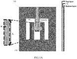
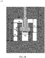
- FIG. 1A and FIG. 1B show a schematic structure of a resonant unit 100 according to an embodiment of the present invention.
- the resonant unit 100 includes:
- an embedded interdigital structure 160 is introduced in a defected ground structure 130 in a resonant unit 100. Therefore, a high-order harmonic wave in a base frequency signal is pushed to a higher frequency, a harmonic suppression capability of the resonant unit 100 is improved, the resonant unit 100 has a wide stopband with higher suppression, and an area of the resonant unit 100 is reduced.
- a filter provided by an embodiment of the present invention includes at least two resonant units 100 described above.
- the filter including the resonant units 100 can improve an out-band suppression capability of the filter and reduce an area of the filter.
- each embedded interdigital structure 160 in the at least one embedded interdigital structure 160 may introduce a resonant frequency of the resonant unit. Therefore, the embedded interdigital structure 160 disposed in the defected ground structure of the resonant unit introduces a new resonant frequency, and a resonant unit having multiple resonant points is formed.
- the resonant unit having multiple resonant points has an ultra wide out-band harmonic suppression capability. In addition, an area occupied by the resonant unit is small.
- the metal microstrip 120 may be a T-shaped microstrip.
- a T-shaped vertical end of the T-shaped microstrip may be used as a signal input/output port.
- the metal microstrip 120 may also be in other shapes, and this is not limited in this embodiment of the present invention.
- a projection of a T-shaped horizontal end of the T-shaped microstrip on a plane of the dielectric substrate 110 may overlap at least a part of the multiple fingers of the interdigital structure 150, and a projection of the T-shaped vertical end on the plane overlaps one finger in the multiple fingers of the interdigital structure 150.
- the projection of the T-shaped horizontal end of the T-shaped microstrip on the plane may overlap all of the multiple fingers of the interdigital structure.
- a shape of the ground loop 140 in this embodiment of the present invention is not limited.
- the ground loop 140 may be rectangular.
- the interdigital structure 150 may include multiple fingers, one end of any finger in the multiple fingers may be connected to the ground loop, and the other end of the any finger may be an open end. The open end is not connected to the ground loop.
- the at least one embedded interdigital structure 160 may be located on a finger of the interdigital structure 150, and/or located on the ground loop 140. In other words, the at least one embedded interdigital structure 160 may be located in any position in the defected ground structure 130.
- the interdigital structure 150 may introduce a resonant frequency of the resonant unit 100, and this resonant frequency may be referred to as a first base frequency (f 01 ).
- a value of the first base frequency may be determined by at least one of the following parameters: a length or a width of a finger included in the interdigital structure 150, or a distance between a finger and the ground loop.
- the first base frequency may be reduced by increasing lengths of L 1 , L 2 , L 3 , W 1 , W 2 , and W 3 .
- L 1B is a rectangular ground loop
- L 1 indicates a length of a side of the rectangular ground loop
- L 2 and L 3 indicate lengths of fingers included in the interdigital structure 150
- the finger of the length L 2 and the finger of the length L 3 are cross-arranged.
- W 1 and W 2 indicate distances between each finger and a side of the rectangular ground loop
- W 3 indicates a width of a finger.
- each embedded interdigital structure 160 in the at least one embedded interdigital structure 160 may introduce a resonant frequency of the resonant unit 100 independently.
- This resonant frequency may also be referred to as a base frequency or a center frequency of the resonant unit 100.
- the resonant frequency introduced by the embedded interdigital structure 160 may be referred to as a second base frequency (f 02 ) or a third base frequency (f 03 ).
- a value of the resonant frequency introduced by each embedded interdigital structure 160 may be determined by at least one of the following parameters: a quantity of fingers in each embedded interdigital structure 160, a width of a finger in each embedded interdigital structure 160, or a length of a finger in each embedded interdigital structure 160.
- the resonant frequency introduced by each embedded interdigital structure 160 may be reduced by increasing the quantity of fingers in each embedded interdigital structure 160, the width (W s ) of a finger, or the length (L s ) of a finger.
- values of resonant frequencies may be trimmed by adjusting the width W t of the T-shaped horizontal end, the length L t1 of the T-shaped horizontal end, and the length L t2 of the T-shaped vertical end of the T-shaped microstrip.
- values of base frequencies of the resonant unit 100 may be trimmed by adjusting lengths L t1 , L t2 , and W t of the T-shaped microstrip.
- the multiple embedded interdigital structures 160 in the resonant unit 100 may have different sizes. Therefore, multiple resonant points (namely, resonant frequencies) are introduced, and a slow-wave resonant unit having multiple resonant points is formed. The resonant points introduced by the embedded interdigital structures 160 are independent of each other.
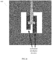
- FIG. 2 to FIG. 4 show schematic structural diagrams of a resonant unit according to another embodiment of the present invention.
- a person skilled in the art can understand that, examples in FIG. 2 to FIG. 4 are merely intended to help a person skilled in the art understand this embodiment of the present invention, and this embodiment of the present invention is not limited to illustrated specific scenarios. This embodiment of the present invention is intended to cover the modifications and variations.
- a quantity of fingers, and a quantity and locations of embedded interdigital structures in an interdigital structure in this embodiment of the present invention are not limited.
- An embedded interdigital structure may be located on each finger of the interdigital structure, or may be located on a finger of the interdigital structure, or may be located on a ground loop.
- a resonant unit 200 shown in FIG. 2 includes four embedded interdigital structures, and the embedded interdigital structures may be located on a ground loop or two fingers in three fingers of an interdigital structure.
- a resonant unit 300 shown in FIG. 3 includes an embedded interdigital structure, and the embedded interdigital structure may be located on one finger in two fingers of an interdigital structure.
- a resonant unit 400 includes two embedded interdigital structures, and the two embedded interdigital structures may be respectively located on two fingers included in the interdigital structure.
- an embodiment of the present invention provides a filter including the foregoing resonant unit.
- the filter may be a band-pass filter, or may be a band-stop filter.
- the filter may be a multi-passband band-pass filter, or may be a multi-stopband band-stop filter.
- an embedded interdigital structure is disposed directly below a metal microstrip, and a band-stop filter may be formed. More specifically, being directly below the metal microstrip may mean that the embedded interdigital structure is disposed in an area using a central axis of a projection of the metal microstrip (namely, a projection of the metal microstrip on a plane in which the defected ground structure is located) as a symmetry axis.
- a transmission zero may be introduced for the filter, that is, a band-stop filter is formed.
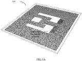
- FIG. 5A and FIG. 5B show two manners of introducing a transmission zero for a filter.
- An embedded interdigital structure in a resonant unit 510 and a resonant unit 520 in FIG. 5A and FIG. 5B is symmetric along a central axis in an area covered by a projection of a T-shaped microstrip. Therefore, a transmission zero is introduced for a filter to form a band-stop filter.
- an embedded interdigital structure is disposed in another area not directly below a metal microstrip, and a band-pass filter may be formed.
- a band-pass filter as an example, the following describes a filter provided by an embodiment of the present invention.
- an embedded interdigital structure is introduced in a defected ground structure in a resonant unit included in a filter. Therefore, a high-order harmonic wave in a base frequency signal is pushed to a higher frequency, a harmonic suppression capability of the filter is improved, the filter has a wide stopband with higher suppression, and an area of the filter is reduced.
- FIG. 6 is a schematic diagram of a filter 600 according to an embodiment of the present invention.
- a band-pass filter may be formed by cascading at least two resonant units.
- either of two resonant units introduced in FIG. 6 includes two embedded interdigital structures, that is, either of the two resonant units includes three resonant frequencies.
- the two resonant units having three resonant frequencies are cascaded, and a second-order three-passband band-pass filter may be obtained.
- a metal microstrip of a resonant unit may be used as an input/output port of the band-pass filter.
- any multi-passband band-pass filter may be implemented. That is, at least two resonant units having N resonant frequencies are cascaded, and an N-passband band-pass filter may be obtained, where N is an integer greater than or equal to 1.
- the resonant units included in the filter may be extended by multi-level cascading, so that an ultra wide stopband multi-order band-pass filter is obtained.
- stopband suppression performance of the filter is enhanced, and steepness of a passband is increased.
- FIG. 7 shows a schematic diagram of a filter 700 according to another embodiment of the present invention. As shown in FIG. 7 , three resonant units are cascaded, and a third-order band-pass filter (a third-order three-passband band-pass filter shown in FIG. 7 ) may be obtained.
- the cascading manner may be applied to cascading of any plurality of resonant units having any plurality of frequencies.
- the resonant units in the filter may be cascaded in a manner of magnetic coupling cascading, electric coupling cascading, or through-hole cascading.
- the magnetic coupling cascading manner is shown in a filter 800 in FIG. 8 .
- Resonant units are cascaded by means of direct connection (as shown by a dashed line in FIG. 8 ).
- the electric coupling cascading manner is shown in a filter 900 in FIG. 9 . That is, resonant units are not directly connected to each other; a broadside couple manner (as shown by a dashed line in the figure) is used instead.
- resonant units are cascaded by means of through-hole connection.
- a through-hole is added in an overlapping part of the resonant units (as shown by a dashed line in the figure), and coupling intensity is increased by means of mixed coupling.
- the three cascading manners may be applicable to connecting any plurality of resonant units, and may be mixed in use.
- metal microstrips of multiple cascaded resonant units may be used as input/output ports of a filter, and may be located on a same side of the resonant units (as shown in FIG. 8 ), or may be located on different sides of the resonant units (as shown in FIG. 6 and FIG. 7 ). This is not limited in this embodiment of the present invention.
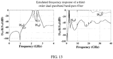
- FIG. 11 to FIG. 13 show emulation results of filters according to the embodiments of the present invention.
- S21 and S11 indicate S parameters
- S21 indicates a transmission factor from a port 2 (output port) to a port 1 (input port)
- S11 indicates a reflection factor seen from the port 1.
- the two parameters are both greater than 0 but are not greater than 1, and are generally measured in dB.
- Greater S21 indicates that more energy is transmitted from the port 1 to the port 2.
- Greater S11 indicates that most of energy input from the port 1 is reflected back and does not arrive at the port 2.
- FIG. 11 shows an emulation result of a second-order dual-passband band-pass filter.
- This filter is formed by cascading two resonant units having two resonant frequencies.
- the resonant frequencies of the filter are respectively 2.21 GHz and 2.47 GHz
- a spacing between resonant frequencies of passbands is 260 MHz
- a stopband may be extended to 19.7 times that of a first base frequency (2.21 GHz) or 17.6 times that of a second base frequency (2.47 GHz)
- suppression reaches -26.3 dB.
- FIG. 12 shows an emulation result of a second-order three-passband band-pass filter.
- This filter is formed by cascading two resonant units having three resonant frequencies.
- the resonant frequencies of the filter are respectively 2.24 GHz, 2.44 GHz, and 2.69 GHz
- spacings between resonant frequencies of adjacent channels are respectively 200 MHz and 250MHz
- a stopband may be extended to 20.7 times that of a first base frequency (2.24 GHz), 19.1 times that of a second base frequency (2.44 GHz), or 17.3 times that of a third base frequency (2.69 GHz)
- suppression reaches -28.6 dB.
- the filters provided by the embodiments of the present invention have high out-band suppression capabilities and small spacings between resonant frequencies, and may be applicable to more scenarios.
- FIG. 13 shows an emulation result of a third-order dual-passband band-pass filter.
- This filter is formed by cascading three resonant units having two resonant frequencies.
- the resonant frequencies of the filter are respectively 2.16 GHz and 2.52 GHz
- a spacing between resonant frequencies of passbands is 360 MHz
- a stopband may be extended to 18.5 times that of a first base frequency (2.16 GHz) or 15.9 times that of a second base frequency (2.52 GHz)
- suppression reaches -31.5 dB.
- the filters in the embodiments of the present invention can improve filter out-band suppression capabilities.
- the terms "system” and “network” may be used interchangeably in this specification.
- the term “and/or” in this specification describes only an association relationship for describing associated objects and represents that three relationships may exist. For example, A and/or B may represent the following three cases: Only A exists, both A and B exist, and only B exists.
- the character "/" in this specification generally indicates an "or” relationship between the associated objects.
- the input/output port may be used as an input port or an output port, or may be simultaneously used as an input and output port. In the filters in FIG. 5 to FIG. 10 , when multiple resonant units are cascaded, an input/output port of any resonant unit may be used as a signal input port, and an input/output port of another resonant unit may be used as a signal output port.
Landscapes
- Physics & Mathematics (AREA)
- Electromagnetism (AREA)
- Control Of Motors That Do Not Use Commutators (AREA)
Claims (12)
- Resonanzeinheit (100), umfassend:ein dielektrisches Substrat (110);einen metallischen Mikrostreifen (120), der auf einer Fläche des dielektrischen Substrats (110) angeordnet ist, wobei der metallische Mikrostreifen (120) als ein Signaleingangs-/Signalausgangsport verwendet wird; undeine Defekt-Masse-Struktur (130), die auf einer anderen Fläche angeordnet ist, gegenüber der Fläche des dielektrischen Substrats (110), auf der der metallische Mikrostreifen (120) angeordnet ist, wobei die Defekt-Masse-Struktur (130) eine Masseschleife (140) und eine Interdigitalstruktur (150), die sich in der Masseschleife (140) befindet, umfasst, wobei die Interdigitalstruktur (150) mehrere Finger umfasst,dadurch gekennzeichnet dasswenigstens ein Finger in der Interdigitalstruktur (150) wenigstens eine eingebettete Interdigitalstruktur (160) umfasst.
- Resonanzeinheit (100) nach Anspruch 1, wobei jede eingebettete Interdigitalstruktur (160) in der wenigstens einen eingebetteten Interdigitalstruktur (160) verwendet wird, um eine Resonanzfrequenz der Resonanzeinheit (100) einzuführen.
- Resonanzeinheit (100) nach Anspruch 2, wobei ein Wert der Resonanzfrequenz durch wenigstens einen der folgenden Parameter bestimmt wird: eine Menge von Fingern in jeder eingebetteten Interdigitalstruktur (160), eine Breite eines Fingers in jeder eingebetteten Interdigitalstruktur (160) oder eine Länge eines Fingers in jeder eingebetteten Interdigitalstruktur (160).
- Resonanzeinheit (100) nach einem der Ansprüche 1 bis 3, wobei es sich bei den mehreren Fingern um drei Finger handelt und sich wenigstens ein Teil der wenigstens einen eingebetteten Interdigitalstruktur (160) auf wenigstens einem Finger der drei Finger befindet.
- Resonanzeinheit (100) nach einem der Ansprüche 1 bis 3, wobei es sich bei den mehreren Fingern um zwei Finger handelt und sich wenigstens ein Teil der wenigstens einen eingebetteten Interdigitalstruktur (160) auf wenigstens einem Finger der zwei Finger befindet.
- Resonanzeinheit (100) nach einem der Ansprüche 1 bis 5, wobei es sich bei dem metallischen Mikrostreifen (120) um einen T-förmigen Mikrostreifen handelt und ein T-förmiges vertikales Ende des T-förmigen Mikrostreifens als der Eingangs-/Ausgangsport verwendet wird.
- Resonanzeinheit (100) nach Anspruch 6, wobei ein Vorsprung eines T-förmigen horizontalen Endes des T-förmigen Mikrostreifens auf der Fläche wenigstens einen Teil der mehreren Finger überlappt und ein Vorsprung des T-förmigen vertikalen Endes auf der Fläche einen Finger der mehreren Finger überlappt.
- Resonanzeinheit (100) nach Anspruch 7, wobei der Vorsprung des T-förmigen horizontalen Endes auf der Fläche alle der mehreren Finger überlappt.
- Filter (600), umfassend wenigstens zwei Resonanzeinheiten (100) nach einem der Ansprüche 1 bis 8, wobei die wenigstens zwei Resonanzeinheiten (100) kaskadiert sind.
- Filter (600) nach Anspruch 9, wobei die wenigstens zwei Resonanzeinheiten (100) in wenigstens einer der folgenden Weisen kaskadiert sind: Durchgangslochkaskadierung, Kaskadierung mit elektrischer Kopplung oder Kaskadierung mit magnetischer Kopplung.
- Filter (600) nach Anspruch 9 oder 10, wobei Strukturen der wenigstens zwei Resonanzeinheiten (100) die gleichen sind.
- Kommunikationssystem, umfassend das Filter nach einem der Ansprüche 9 bis 11.
Applications Claiming Priority (1)
| Application Number | Priority Date | Filing Date | Title |
|---|---|---|---|
| CN201610428290.9A CN106099278B (zh) | 2016-06-16 | 2016-06-16 | 谐振单元和滤波器 |
Publications (2)
| Publication Number | Publication Date |
|---|---|
| EP3258535A1 EP3258535A1 (de) | 2017-12-20 |
| EP3258535B1 true EP3258535B1 (de) | 2020-03-11 |
Family
ID=57235563
Family Applications (1)
| Application Number | Title | Priority Date | Filing Date |
|---|---|---|---|
| EP17175812.1A Active EP3258535B1 (de) | 2016-06-16 | 2017-06-13 | Resonanzeinheit und filter mit defected-ground-struktur |
Country Status (3)
| Country | Link |
|---|---|
| US (1) | US10276904B2 (de) |
| EP (1) | EP3258535B1 (de) |
| CN (1) | CN106099278B (de) |
Families Citing this family (10)
| Publication number | Priority date | Publication date | Assignee | Title |
|---|---|---|---|---|
| US10172005B2 (en) | 2017-04-24 | 2019-01-01 | International Business Machines Corporation | Resonance frequency device locking |
| US10149167B2 (en) | 2017-04-24 | 2018-12-04 | International Business Machines Corporation | Mobile device locking |
| CN111082191B (zh) * | 2019-12-25 | 2021-02-02 | 南通大学附属医院 | 一种通道能够独立设计的双工器 |
| CN111181519A (zh) * | 2019-12-26 | 2020-05-19 | 安徽安努奇科技有限公司 | 多工器电路和多工器设备 |
| CN112803128B (zh) * | 2020-12-31 | 2025-12-16 | 江门职业技术学院 | 微带低通滤波器 |
| CN115206377A (zh) * | 2022-05-09 | 2022-10-18 | 中国人民武装警察部队海警学院 | 内嵌交叉结构的亚阈值p-p-n型10管存储单元 |
| CN115528400B (zh) * | 2022-10-11 | 2026-02-10 | 成都威频科技有限公司 | 一种高矩形系数带状线低通滤波器 |
| CN115911795B (zh) * | 2022-10-28 | 2024-10-01 | 厦门大学 | 基片集成人工表面等离激元多通带滤波器 |
| CN115764217A (zh) * | 2022-11-21 | 2023-03-07 | 苏州科技大学 | 一种基于非对称光子晶体Tamm态的微波二极管 |
| CN116613491B (zh) * | 2023-07-18 | 2023-10-13 | 成都华兴汇明科技有限公司 | 一种具有三个传输零点的选频网络及其构造的微波振荡器 |
Family Cites Families (7)
| Publication number | Priority date | Publication date | Assignee | Title |
|---|---|---|---|---|
| KR100349571B1 (ko) * | 2000-07-04 | 2002-08-24 | 안달 | 유전체의 접지면에 식각된 결함 구조를 갖는 공진기 |
| KR20050060279A (ko) * | 2003-12-16 | 2005-06-22 | 세원텔레텍 주식회사 | 2차 주파수 체배기 및 그 설계방법 |
| KR101040426B1 (ko) * | 2009-06-05 | 2011-06-09 | 순천향대학교 산학협력단 | 주파수 가변성을 갖는 쌍대 합성 우좌향 전송선로 구조 |
| CN202550038U (zh) * | 2011-12-10 | 2012-11-21 | 哈尔滨飞羽科技有限公司 | 一种陷波陡峭的uwb双陷波滤波器 |
| CN103545584B (zh) * | 2013-10-31 | 2015-09-23 | 西南大学 | 一种低插损宽带带通滤波器 |
| CN105680126A (zh) * | 2015-12-30 | 2016-06-15 | 联想(北京)有限公司 | 一种滤波器调节方法、滤波器及电子设备 |
| US9997817B2 (en) | 2015-12-30 | 2018-06-12 | Lenovo (Beijing) Limited | Filter and electronic device |
-
2016
- 2016-06-16 CN CN201610428290.9A patent/CN106099278B/zh active Active
-
2017
- 2017-06-13 EP EP17175812.1A patent/EP3258535B1/de active Active
- 2017-06-16 US US15/625,374 patent/US10276904B2/en active Active
Non-Patent Citations (1)
| Title |
|---|
| None * |
Also Published As
| Publication number | Publication date |
|---|---|
| CN106099278A (zh) | 2016-11-09 |
| US10276904B2 (en) | 2019-04-30 |
| CN106099278B (zh) | 2019-02-19 |
| EP3258535A1 (de) | 2017-12-20 |
| US20170365903A1 (en) | 2017-12-21 |
Similar Documents
| Publication | Publication Date | Title |
|---|---|---|
| US10276904B2 (en) | Resonant unit and filter | |
| Liu et al. | Substrate integrated waveguide bandpass filters in box-like topology with bypass and direct couplings in diagonal cross-coupling path | |
| CN102361110B (zh) | 小型化双模双频微带滤波器 | |
| Shen et al. | A novel microstrip filter using three-mode stepped impedance resonator (TSIR) | |
| Sun et al. | Multiple-resonator-based bandpass filters | |
| US9711833B1 (en) | Tunable RF anti-jamming system (TRAJS) | |
| KR20150112179A (ko) | 차단성능 향상을 위해 접지 스터브를 사용한 도파관 대역통과필터 | |
| CN110137643A (zh) | 一种带宽可控的大频率比同轴腔双频滤波器 | |
| CN112928409A (zh) | 具有宽阻带和高选择性的微带带通滤波器 | |
| Ammar et al. | Efficient diplexer with high selectivity and low insertion loss based on SOLR and DGS for WIMAX | |
| Kumar et al. | Design of improved quadruple-mode bandpass filter using cavity resonator for 5G mid-band applications | |
| CN108110388B (zh) | 电调传输零点的恒定带宽宽带滤波器 | |
| US10673111B2 (en) | Filtering unit and filter | |
| Afridi et al. | Monolithic ceramic waveguide filter with wide spurious free bandwidth | |
| JPH10322155A (ja) | 帯域阻止フィルタ | |
| Mehrshahi et al. | Substrate integrated waveguide filters with stopband performance improvement | |
| Doumanis et al. | Inline interdigital pseudo-elliptic helical resonator filters | |
| Doumanis et al. | Transmission zero realization in E-plane filters by means of I/O resonator tapping | |
| CN111900518B (zh) | 一种具有180度移相器的介质滤波器 | |
| Martínez et al. | Compact SIW filter with asymmetric frequency response for C-band wireless applications | |
| KR100541068B1 (ko) | 유전체필터를 갖춘 중계기 | |
| Lahmissi et al. | Microstrip dual-band bandpass filter design using folded coupled lines | |
| CN104332680B (zh) | 一种方形谐振环的微带双模带通滤波器 | |
| Thabet et al. | Minimization and optimization in the performance of dual-band BPF by using E-shape microstrip structure | |
| Li et al. | Dual-notch ultra-wideband bandpass filter based on folded dual-mode resonator |
Legal Events
| Date | Code | Title | Description |
|---|---|---|---|
| PUAI | Public reference made under article 153(3) epc to a published international application that has entered the european phase |
Free format text: ORIGINAL CODE: 0009012 |
|
| STAA | Information on the status of an ep patent application or granted ep patent |
Free format text: STATUS: THE APPLICATION HAS BEEN PUBLISHED |
|
| AK | Designated contracting states |
Kind code of ref document: A1 Designated state(s): AL AT BE BG CH CY CZ DE DK EE ES FI FR GB GR HR HU IE IS IT LI LT LU LV MC MK MT NL NO PL PT RO RS SE SI SK SM TR |
|
| AX | Request for extension of the european patent |
Extension state: BA ME |
|
| STAA | Information on the status of an ep patent application or granted ep patent |
Free format text: STATUS: REQUEST FOR EXAMINATION WAS MADE |
|
| 17P | Request for examination filed |
Effective date: 20180308 |
|
| RBV | Designated contracting states (corrected) |
Designated state(s): AL AT BE BG CH CY CZ DE DK EE ES FI FR GB GR HR HU IE IS IT LI LT LU LV MC MK MT NL NO PL PT RO RS SE SI SK SM TR |
|
| GRAP | Despatch of communication of intention to grant a patent |
Free format text: ORIGINAL CODE: EPIDOSNIGR1 |
|
| STAA | Information on the status of an ep patent application or granted ep patent |
Free format text: STATUS: GRANT OF PATENT IS INTENDED |
|
| INTG | Intention to grant announced |
Effective date: 20190920 |
|
| GRAS | Grant fee paid |
Free format text: ORIGINAL CODE: EPIDOSNIGR3 |
|
| GRAA | (expected) grant |
Free format text: ORIGINAL CODE: 0009210 |
|
| STAA | Information on the status of an ep patent application or granted ep patent |
Free format text: STATUS: THE PATENT HAS BEEN GRANTED |
|
| AK | Designated contracting states |
Kind code of ref document: B1 Designated state(s): AL AT BE BG CH CY CZ DE DK EE ES FI FR GB GR HR HU IE IS IT LI LT LU LV MC MK MT NL NO PL PT RO RS SE SI SK SM TR |
|
| REG | Reference to a national code |
Ref country code: GB Ref legal event code: FG4D |
|
| REG | Reference to a national code |
Ref country code: CH Ref legal event code: EP |
|
| REG | Reference to a national code |
Ref country code: AT Ref legal event code: REF Ref document number: 1244312 Country of ref document: AT Kind code of ref document: T Effective date: 20200315 |
|
| REG | Reference to a national code |
Ref country code: IE Ref legal event code: FG4D |
|
| REG | Reference to a national code |
Ref country code: DE Ref legal event code: R096 Ref document number: 602017012808 Country of ref document: DE |
|
| PG25 | Lapsed in a contracting state [announced via postgrant information from national office to epo] |
Ref country code: RS Free format text: LAPSE BECAUSE OF FAILURE TO SUBMIT A TRANSLATION OF THE DESCRIPTION OR TO PAY THE FEE WITHIN THE PRESCRIBED TIME-LIMIT Effective date: 20200311 Ref country code: FI Free format text: LAPSE BECAUSE OF FAILURE TO SUBMIT A TRANSLATION OF THE DESCRIPTION OR TO PAY THE FEE WITHIN THE PRESCRIBED TIME-LIMIT Effective date: 20200311 Ref country code: NO Free format text: LAPSE BECAUSE OF FAILURE TO SUBMIT A TRANSLATION OF THE DESCRIPTION OR TO PAY THE FEE WITHIN THE PRESCRIBED TIME-LIMIT Effective date: 20200611 |
|
| REG | Reference to a national code |
Ref country code: NL Ref legal event code: MP Effective date: 20200311 |
|
| PG25 | Lapsed in a contracting state [announced via postgrant information from national office to epo] |
Ref country code: BG Free format text: LAPSE BECAUSE OF FAILURE TO SUBMIT A TRANSLATION OF THE DESCRIPTION OR TO PAY THE FEE WITHIN THE PRESCRIBED TIME-LIMIT Effective date: 20200611 Ref country code: SE Free format text: LAPSE BECAUSE OF FAILURE TO SUBMIT A TRANSLATION OF THE DESCRIPTION OR TO PAY THE FEE WITHIN THE PRESCRIBED TIME-LIMIT Effective date: 20200311 Ref country code: LV Free format text: LAPSE BECAUSE OF FAILURE TO SUBMIT A TRANSLATION OF THE DESCRIPTION OR TO PAY THE FEE WITHIN THE PRESCRIBED TIME-LIMIT Effective date: 20200311 Ref country code: GR Free format text: LAPSE BECAUSE OF FAILURE TO SUBMIT A TRANSLATION OF THE DESCRIPTION OR TO PAY THE FEE WITHIN THE PRESCRIBED TIME-LIMIT Effective date: 20200612 Ref country code: HR Free format text: LAPSE BECAUSE OF FAILURE TO SUBMIT A TRANSLATION OF THE DESCRIPTION OR TO PAY THE FEE WITHIN THE PRESCRIBED TIME-LIMIT Effective date: 20200311 |
|
| REG | Reference to a national code |
Ref country code: LT Ref legal event code: MG4D |
|
| PG25 | Lapsed in a contracting state [announced via postgrant information from national office to epo] |
Ref country code: NL Free format text: LAPSE BECAUSE OF FAILURE TO SUBMIT A TRANSLATION OF THE DESCRIPTION OR TO PAY THE FEE WITHIN THE PRESCRIBED TIME-LIMIT Effective date: 20200311 |
|
| PG25 | Lapsed in a contracting state [announced via postgrant information from national office to epo] |
Ref country code: LT Free format text: LAPSE BECAUSE OF FAILURE TO SUBMIT A TRANSLATION OF THE DESCRIPTION OR TO PAY THE FEE WITHIN THE PRESCRIBED TIME-LIMIT Effective date: 20200311 Ref country code: SK Free format text: LAPSE BECAUSE OF FAILURE TO SUBMIT A TRANSLATION OF THE DESCRIPTION OR TO PAY THE FEE WITHIN THE PRESCRIBED TIME-LIMIT Effective date: 20200311 Ref country code: PT Free format text: LAPSE BECAUSE OF FAILURE TO SUBMIT A TRANSLATION OF THE DESCRIPTION OR TO PAY THE FEE WITHIN THE PRESCRIBED TIME-LIMIT Effective date: 20200805 Ref country code: IS Free format text: LAPSE BECAUSE OF FAILURE TO SUBMIT A TRANSLATION OF THE DESCRIPTION OR TO PAY THE FEE WITHIN THE PRESCRIBED TIME-LIMIT Effective date: 20200711 Ref country code: RO Free format text: LAPSE BECAUSE OF FAILURE TO SUBMIT A TRANSLATION OF THE DESCRIPTION OR TO PAY THE FEE WITHIN THE PRESCRIBED TIME-LIMIT Effective date: 20200311 Ref country code: CZ Free format text: LAPSE BECAUSE OF FAILURE TO SUBMIT A TRANSLATION OF THE DESCRIPTION OR TO PAY THE FEE WITHIN THE PRESCRIBED TIME-LIMIT Effective date: 20200311 Ref country code: SM Free format text: LAPSE BECAUSE OF FAILURE TO SUBMIT A TRANSLATION OF THE DESCRIPTION OR TO PAY THE FEE WITHIN THE PRESCRIBED TIME-LIMIT Effective date: 20200311 Ref country code: EE Free format text: LAPSE BECAUSE OF FAILURE TO SUBMIT A TRANSLATION OF THE DESCRIPTION OR TO PAY THE FEE WITHIN THE PRESCRIBED TIME-LIMIT Effective date: 20200311 |
|
| REG | Reference to a national code |
Ref country code: AT Ref legal event code: MK05 Ref document number: 1244312 Country of ref document: AT Kind code of ref document: T Effective date: 20200311 |
|
| REG | Reference to a national code |
Ref country code: DE Ref legal event code: R097 Ref document number: 602017012808 Country of ref document: DE |
|
| REG | Reference to a national code |
Ref country code: DE Ref legal event code: R119 Ref document number: 602017012808 Country of ref document: DE |
|
| PLBE | No opposition filed within time limit |
Free format text: ORIGINAL CODE: 0009261 |
|
| STAA | Information on the status of an ep patent application or granted ep patent |
Free format text: STATUS: NO OPPOSITION FILED WITHIN TIME LIMIT |
|
| PG25 | Lapsed in a contracting state [announced via postgrant information from national office to epo] |
Ref country code: IT Free format text: LAPSE BECAUSE OF FAILURE TO SUBMIT A TRANSLATION OF THE DESCRIPTION OR TO PAY THE FEE WITHIN THE PRESCRIBED TIME-LIMIT Effective date: 20200311 Ref country code: MC Free format text: LAPSE BECAUSE OF FAILURE TO SUBMIT A TRANSLATION OF THE DESCRIPTION OR TO PAY THE FEE WITHIN THE PRESCRIBED TIME-LIMIT Effective date: 20200311 Ref country code: DK Free format text: LAPSE BECAUSE OF FAILURE TO SUBMIT A TRANSLATION OF THE DESCRIPTION OR TO PAY THE FEE WITHIN THE PRESCRIBED TIME-LIMIT Effective date: 20200311 Ref country code: ES Free format text: LAPSE BECAUSE OF FAILURE TO SUBMIT A TRANSLATION OF THE DESCRIPTION OR TO PAY THE FEE WITHIN THE PRESCRIBED TIME-LIMIT Effective date: 20200311 Ref country code: AT Free format text: LAPSE BECAUSE OF FAILURE TO SUBMIT A TRANSLATION OF THE DESCRIPTION OR TO PAY THE FEE WITHIN THE PRESCRIBED TIME-LIMIT Effective date: 20200311 |
|
| REG | Reference to a national code |
Ref country code: CH Ref legal event code: PL |
|
| 26N | No opposition filed |
Effective date: 20201214 |
|
| PG25 | Lapsed in a contracting state [announced via postgrant information from national office to epo] |
Ref country code: SI Free format text: LAPSE BECAUSE OF FAILURE TO SUBMIT A TRANSLATION OF THE DESCRIPTION OR TO PAY THE FEE WITHIN THE PRESCRIBED TIME-LIMIT Effective date: 20200311 Ref country code: PL Free format text: LAPSE BECAUSE OF FAILURE TO SUBMIT A TRANSLATION OF THE DESCRIPTION OR TO PAY THE FEE WITHIN THE PRESCRIBED TIME-LIMIT Effective date: 20200311 |
|
| PG25 | Lapsed in a contracting state [announced via postgrant information from national office to epo] |
Ref country code: LU Free format text: LAPSE BECAUSE OF NON-PAYMENT OF DUE FEES Effective date: 20200613 |
|
| REG | Reference to a national code |
Ref country code: BE Ref legal event code: MM Effective date: 20200630 |
|
| PG25 | Lapsed in a contracting state [announced via postgrant information from national office to epo] |
Ref country code: IE Free format text: LAPSE BECAUSE OF NON-PAYMENT OF DUE FEES Effective date: 20200613 Ref country code: FR Free format text: LAPSE BECAUSE OF NON-PAYMENT OF DUE FEES Effective date: 20200630 Ref country code: CH Free format text: LAPSE BECAUSE OF NON-PAYMENT OF DUE FEES Effective date: 20200630 Ref country code: LI Free format text: LAPSE BECAUSE OF NON-PAYMENT OF DUE FEES Effective date: 20200630 |
|
| PG25 | Lapsed in a contracting state [announced via postgrant information from national office to epo] |
Ref country code: BE Free format text: LAPSE BECAUSE OF NON-PAYMENT OF DUE FEES Effective date: 20200630 Ref country code: DE Free format text: LAPSE BECAUSE OF NON-PAYMENT OF DUE FEES Effective date: 20210101 |
|
| PG25 | Lapsed in a contracting state [announced via postgrant information from national office to epo] |
Ref country code: TR Free format text: LAPSE BECAUSE OF FAILURE TO SUBMIT A TRANSLATION OF THE DESCRIPTION OR TO PAY THE FEE WITHIN THE PRESCRIBED TIME-LIMIT Effective date: 20200311 Ref country code: MT Free format text: LAPSE BECAUSE OF FAILURE TO SUBMIT A TRANSLATION OF THE DESCRIPTION OR TO PAY THE FEE WITHIN THE PRESCRIBED TIME-LIMIT Effective date: 20200311 Ref country code: CY Free format text: LAPSE BECAUSE OF FAILURE TO SUBMIT A TRANSLATION OF THE DESCRIPTION OR TO PAY THE FEE WITHIN THE PRESCRIBED TIME-LIMIT Effective date: 20200311 |
|
| PG25 | Lapsed in a contracting state [announced via postgrant information from national office to epo] |
Ref country code: MK Free format text: LAPSE BECAUSE OF FAILURE TO SUBMIT A TRANSLATION OF THE DESCRIPTION OR TO PAY THE FEE WITHIN THE PRESCRIBED TIME-LIMIT Effective date: 20200311 Ref country code: AL Free format text: LAPSE BECAUSE OF FAILURE TO SUBMIT A TRANSLATION OF THE DESCRIPTION OR TO PAY THE FEE WITHIN THE PRESCRIBED TIME-LIMIT Effective date: 20200311 |
|
| PGFP | Annual fee paid to national office [announced via postgrant information from national office to epo] |
Ref country code: GB Payment date: 20250501 Year of fee payment: 9 |